EP3696834A1 - Metall-polymer-kapazität, die eine dielektrische folie mit einer starken dielektrischen konstante und einer starken durchbruchfeldstärke umfasst - Google Patents
Metall-polymer-kapazität, die eine dielektrische folie mit einer starken dielektrischen konstante und einer starken durchbruchfeldstärke umfasst Download PDFInfo
- Publication number
- EP3696834A1 EP3696834A1 EP20157469.6A EP20157469A EP3696834A1 EP 3696834 A1 EP3696834 A1 EP 3696834A1 EP 20157469 A EP20157469 A EP 20157469A EP 3696834 A1 EP3696834 A1 EP 3696834A1
- Authority
- EP
- European Patent Office
- Prior art keywords
- nanoparticles
- polymer
- core
- capacity according
- polymer material
- Prior art date
- Legal status (The legal status is an assumption and is not a legal conclusion. Google has not performed a legal analysis and makes no representation as to the accuracy of the status listed.)
- Granted
Links
Images

Classifications
-
- H—ELECTRICITY
- H01—ELECTRIC ELEMENTS
- H01G—CAPACITORS; CAPACITORS, RECTIFIERS, DETECTORS, SWITCHING DEVICES, LIGHT-SENSITIVE OR TEMPERATURE-SENSITIVE DEVICES OF THE ELECTROLYTIC TYPE
- H01G4/00—Fixed capacitors; Processes of their manufacture
- H01G4/002—Details
- H01G4/018—Dielectrics
- H01G4/06—Solid dielectrics
- H01G4/14—Organic dielectrics
- H01G4/18—Organic dielectrics of synthetic material, e.g. derivatives of cellulose
-
- H—ELECTRICITY
- H01—ELECTRIC ELEMENTS
- H01G—CAPACITORS; CAPACITORS, RECTIFIERS, DETECTORS, SWITCHING DEVICES, LIGHT-SENSITIVE OR TEMPERATURE-SENSITIVE DEVICES OF THE ELECTROLYTIC TYPE
- H01G4/00—Fixed capacitors; Processes of their manufacture
- H01G4/002—Details
- H01G4/018—Dielectrics
- H01G4/06—Solid dielectrics
- H01G4/08—Inorganic dielectrics
-
- H—ELECTRICITY
- H01—ELECTRIC ELEMENTS
- H01G—CAPACITORS; CAPACITORS, RECTIFIERS, DETECTORS, SWITCHING DEVICES, LIGHT-SENSITIVE OR TEMPERATURE-SENSITIVE DEVICES OF THE ELECTROLYTIC TYPE
- H01G4/00—Fixed capacitors; Processes of their manufacture
- H01G4/002—Details
- H01G4/018—Dielectrics
- H01G4/20—Dielectrics using combinations of dielectrics from more than one of groups H01G4/02 - H01G4/06
- H01G4/206—Dielectrics using combinations of dielectrics from more than one of groups H01G4/02 - H01G4/06 inorganic and synthetic material
Definitions
- the present invention relates to the field of capacitors, and more particularly metal-polymer capacitors, in particular for so-called high voltage applications.
- the invention also relates to a method of manufacturing such a metal-polymer capacitor.
- Metal / Insulator / Metal film type capacitors are structures in which a dielectric material is wound between two metal electrodes.
- the dielectric material must be flexible and is generally of the organic type (soaked papers, oils and polymers).
- the films are, for example, in polystyrene (PS), in polyethylene terephthalate (PET), in polytetrafluoroethylene (PTFE), or else in polyetherimide (PEI).
- PS polystyrene
- PET polyethylene terephthalate
- PTFE polytetrafluoroethylene
- PEI polyetherimide
- the ter-polymers poly ((vinylidene fluoride - trifluoroethylene - chlorofluoroethylene) (P (VDF- TrFE-CFE) and poly ((vinylidene fluoride - trifluoroethylene - chlorotrifluoro ethylene) (P (VDF-TrFE-CTFE) are exceptions among dielectric polymers.
- non-polar plasticizers CFE or CTFE
- CFE non-polar plasticizers
- CTFE CTFE
- the ter-polymer is therefore in theory capable of storing 5 times more energy at room temperature than its ferroelectric co-polymer counterpart, the permittivity of which reaches 12.
- the breakdown field of this ter-polymer is of the order of 400MV. / m ( Chu et al.
- a dielectric polymer with high electric energy density and fast discharge speed Science, 313 (5785), 334-336 ). These polar dielectric relaxer polymers are generating a lot of interest in power capacities.
- the low Curie temperature causes a large variation in dielectric properties with temperature, which can be detrimental for power applications which emit a lot of heat.
- the transformation of the piezoelectric character of the copolymer (proportional to V) into electrostrictive character with the terpolymer (proportional to V 2 ) poses a problem because it causes at high voltage a greater mechanical compression of the polymer. By crashing between the electrodes, the capacitor then undergoes a catastrophic increase in the internal electric field (avalanche effect) which leads to its destruction. It is therefore difficult to use this polymer at high voltage.
- the first way is to add oxide nanoparticles in a polymer. More particularly, the polymer is mixed with a high concentration of complex oxide nanoparticles with high permittivity (TiO 2 , SrTiO 3 , BaTiO 3 , PZT, PMNPT, etc.).
- the mixtures are prepared in a homogeneous medium by simple techniques, with stirring.
- the increase in permittivity only becomes substantial for high load rates in accordance with the law of mixtures (Maxwell Garnet), for example for load rates greater than 30% or 50% by mass.
- the nanocomposite material thus formed is subject to strong inhomogeneities of the local electric field at the interface between the high permittivity nanoparticles and the low permittivity polymer.
- the second route consists of mixing the polymer with low concentrations of electrically conductive nanoparticles, for example metallic nanoparticles.
- This is called a metal-polymer composite or a conductor-dielectric composite.
- the concentration of the metallic or conductive phase must remain below the threshold of electrical percolation which in general is low (generally less than 1% by volume), and be controlled with great precision.
- the breakdown resistance can be improved by adding hexagonal boron nitride nanosheets.
- Wu et al. (“Graphene / Boron Nitride-Polyurethane Microlaminates for Exceptional Dielectric Properties and High Energy Densities”. ACS applied materials & interfaces 2018, 10 (31), 26641-26652 ), the breakdown resistance of a reduced oxidized graphene airgel rGO (conductive phase) mixed with polyurethane (dielectric phase) is improved by interposing between the layers of the airgel layers of hexagonal boron nitride nanosheets coated in polyurethane.
- the shaping of such a micro-laminated composite uses cold casting (freeze casting) and compaction (pressing), which is not compatible with many substrates, and in particular with silicon technologies, and does not allow not to realize an integrated capacity.
- An object of the present invention is to provide a capacitor exhibiting high permittivity, few conduction losses and good resistance to electrical voltage.
- the nanoparticles represent from 0.01% to 10%, preferably from 0.01% to 5% and even more preferably from 0.1% to 2% by volume of the dielectric film.
- the nanoparticles with a core / shell structure represent a volume fraction of the dielectric film less than the electrical percolation threshold of the dielectric film.
- the invention differs fundamentally from the prior art, in particular, by the presence of monodisperse metal / polymer hybrid nanoparticles.
- the low size distribution of the nanoparticles, coated with the first polymer material makes it possible to limit or even eliminate interparticle conduction: both direct low voltage conduction paths (local ohmic effect due to the absence of polymer locally) and indirect high voltage (field effect (FET) or tunnel effect through very fine polymer barriers), which increases the permittivity, leads to a reduction in conduction losses and avoids having uncontrolled breakdown fields.
- direct low voltage conduction paths local ohmic effect due to the absence of polymer locally
- FET field effect
- tunnel effect through very fine polymer barriers
- the absence of aggregates and very large nanoparticles is observed (for example having a size or larger dimension up to 100 times, 30 times or 10 times larger than the average size of the nanoparticles) and the absence of very small particles (having a size, for example, up to 6 times or 10 times smaller than the average size of the nanoparticles).
- the nanoparticles are dispersed homogeneously in the polymer matrix.
- the term “homogeneously dispersed” is understood to mean that the nanoparticles are distributed substantially uniformly in the polymer matrix. This makes it possible to further reduce the interparticle conduction.
- the second layer of a polymer material in the shell which coats the nanoparticles.
- the second polymer layer covers at least partially and, preferably, completely the core of the nanoparticles.
- the thickness can, for example, range from 5 to 15nm. It advantageously has a uniform thickness around the nanoparticle.
- the thickness of the layer of second material is substantially identical from one nanoparticle to another. By substantially identical, it is considered that the thickness does not vary by more than 20% from one nanoparticle to another and within the same nanoparticle.
- the presence of the layer of inorganic carbon material makes it possible to covalently graft the layer of polymer material around the nanoparticles.
- the core of the nanoparticles is protected from oxidation by the shell, which allows them to retain their initial properties (for example magnetic and / or electrical).
- the mechanical stability of nanoparticles over time is improved.
- the inorganic carbonaceous material is organized 2D carbon.
- the carbonaceous material is graphene.
- the carbon layer consists of a repetition of a few layers to a few tens of layers of graphene to maintain a 2D organized structure of the carbon.
- it includes a few layers of graphene (from 2 to 5 for example).
- a carbonaceous layer comprising at least two graphene layers will be chosen to impart sufficient hydrophilic properties to the nanoparticle and to be able to form Van der Waals bonds.
- a number of layers less than 100 will be chosen to avoid the appearance of defects in the layers and to have an arrangement of 2D carbon disorganized at the surface, for example hydrogenated, or of the graphitic type which are hydrophobic.
- the carbonaceous layer advantageously forms a continuous layer around each nanoparticle.
- the core of the nanoparticles is made of cobalt, iron, nickel, copper, gold and / or silver.
- the first polymer material is chosen from among polystyrene, polymethyl methacrylate, polyurethane, a polyacrylic, polypropylene, a polyimide, polyetherimide and a polymer having a pyrene group.
- the dielectric film comprises electrically insulating nanoparticles.
- FET tunneling effect
- the dielectric film comprises electrically insulating nanoparticles.
- FET tunneling effect
- the emission of electrons by field effect at the metal / polymer interface can lead to an increase in electrical losses and / or heating which can soften or even melt the polymer coating and / or the host polymer resulting in destruction of the composite material and the capacitor.
- the insertion of electrically insulating nanoparticles makes it possible to limit or even eliminate these undesirable electrical phenomena.
- the capacitance obtained exhibits a strong dielectric constant and a strong breakdown field.
- the electrically insulating nanoparticles are made of metal oxide, for example of barium and / or strontium oxide.
- the electrically insulating nanoparticles are made of a semiconductor material, preferably with a large gap, such as silicon carbide, diamond and / or hexagonal boron nitride.
- a semiconductor material preferably with a large gap, such as silicon carbide, diamond and / or hexagonal boron nitride.
- hexagonal boron nitride it may also be nanotubes and / or nanosheets.
- the electrically insulating nanoparticles are in the shell of the nanoparticles.
- the electrically insulating nanoparticles are in the polymer matrix.
- the dielectric film can comprise an alternation of nanoparticles with a core / shell structure and of electrically insulating nanoparticles.
- Nanoparticles with a core / shell structure and electrically insulating nanoparticles can be dispersed randomly in the matrix.
- the second polymer material is chosen from polystyrene, polyethylene terephthalate, cellulose acetate, polycarbonate, polypropylene, polyethylene, a polyamide, a polysiloxane, a polysulfone, an optionally aromatic polyester, a polyetheretherketone, a polyetherimide and an epoxy.
- the second polymer material comprises groups photosensitive to ultraviolet rays.
- the ratio between the maximum diameter of the nanoparticles and the minimum diameter of the nanoparticles is less than 1.5, preferably less than 1.3, even more preferably less than 1.2 and even more preferably less than 1.1.
- Such a very tight size distribution ensures a strong increase in permittivity.
- a deposition temperature below the melting point of the first polymer material will be chosen.
- emulsion a heterogeneous mixture of two immiscible liquids, such as oil and water.
- One of the two phases (called the dispersed phase, here the aqueous phase) is dispersed in the form of droplets in the other (called the dispersing phase).
- the size of the droplets can range from a few tens of nanometers to 1 micron, for example from 20 nm to 1 ⁇ m.
- mini-emulsion is understood to mean that the size of the droplets can range from 30 nm to 100 nm, and more preferably from 30 nm to 60 nm.
- the droplets of the mini-emulsion form polymerization reactors.
- the monomers will be gradually consumed until the micelle is saturated. We talk about micellar growth.
- the size of the final particle thus formed is similar to that of the micelle.
- a product called latex is obtained comprising monodisperse polymer beads (micelles without metallic nanoparticles) and hybrid metal-polymer nanoparticles (micelles with metallic nanoparticles).
- This polymerization in a heterogeneous medium leads to better control of the thickness of polymer coating the core of the nanoparticles, compared to polymerization in a homogeneous medium.
- the presence of the layer of carbonaceous material surrounding the nanoparticles makes it possible to make the nanoparticles hydrophilic, which allows their insertion into the droplets of the emulsion.
- the layer of carbonaceous material also protects them effectively against oxidation. Without this carbonaceous shell, the metallic nanoparticles would spontaneously oxidize on contact with water and / or form hydroxides, which would make them hydrophobic and would help to drive them out of the micelles to join the dispersing phase (oil).
- the droplets play in addition to a role of polymerization reactor, a role of filter.
- Nanoparticles with a diameter greater than or equal to those of the droplets will form a raw sediment (without polymer) which will be easily removed later.
- the smallest nanoparticles (for example with a diameter of less than 10 nm) are imperfectly covered by the carbon layer and oxidize rapidly (formation of carboxyls and / or metal oxides) , which gives them a more hydrophobic character than nanoparticles completely covered by a carbonaceous layer. These particles do not penetrate into the droplets containing the aqueous phase, remain in suspension in the dispersing phase and can easily be removed subsequently.
- Nanoparticles with a very low size distribution are thus obtained.
- the ratio between the maximum diameter of the nanoparticles and the minimum diameter of the nanoparticles is less than 1.5, preferably less than 1.3, even more preferably less than 1.2 and even more preferably less than 1.1.
- Such a very tight size distribution does not exist commercially and is made possible by the miniemulsion process.
- electrically insulating nanoparticles as defined above are added during step i).
- electrically insulating nanoparticles as defined above are added during step a), b) or c).
- the metal / polymer hybrid capacitor is formed on a substrate 100.
- the substrate 100 is preferably made of silicon.
- Other substrates can be used such as glass, alumina, ferrite and polymeric films such as polyimide (such as Kapton), poly (ethylene naphthalate), and poly (ethylene terephthalate) ) (PET).
- the capacitor comprises a first so-called lower electrode 101, in contact with the substrate 100, and a second so-called upper electrode 102.
- the electrodes are electrically conductive and, preferably, metal. They are, for example, in gold.
- a dielectric film 40 is disposed between the first electrode 101 and the second electrode 102.
- the dielectric film comprises a polymeric matrix 50 in which hybrid metal-polymer nanoparticles are dispersed.
- nanoparticles 20 is meant elements of submicron size (typically less than 1 ⁇ m) of shape, for example, spherical, elongated, ovoid. Preferably, they are spherical particles. Their largest dimension is called diameter or size.
- the nanoparticles 20 are monodispersed, that is to say they have a small size distribution. In other words, they have a size distribution between a maximum diameter and a minimum diameter such that their ratio is less than or equal to 5, 3 or 2 and advantageously less than or equal to 1.5, for example 1.3 or 1.2 or 1.1.
- the characteristics of such a powder are, for example, an average diameter of the nanoparticles of 40nm, a maximum diameter of 42nm and a minimum diameter of 38nm.
- the diameter of the nanoparticles 20 can be measured with a laser particle size analyzer or by light diffraction (DLS for “Dynamic Light Scattering”) in solution.
- the separation distance between the nanoparticles is controlled.
- the edge-to-edge separation distance between two metal / C particles of diameter ⁇ is 1 x ⁇ , 1/2 x ⁇ or 2/3 x ⁇ and advantageously less than or equal to 1/3 x ⁇ .
- such a film is characterized by a homogeneous dispersion of Co / C nanoparticles with an average diameter of 30 nm with an average intergranular distance of 10 nm, up to 5 nm.
- the particles 20 have a core-shell structure.
- the shell 22 is integral with the core 21 of the particle.
- the heart 21, or core is a metallic material.
- metallic material is meant a metal, a metal alloy.
- it is a metal.
- it is cobalt, nickel, iron, copper, silver or gold.
- Such nanoparticles are denoted metal / C / polymer.
- the carbonaceous material is preferably inorganic, for example graphene, graphite or carbon nanotubes.
- it is a 2D carbon coating organized on a non-planar surface (for example on the surface of a nanoparticle).
- the coating 22 is of graphene. It can include one or more (two, three, four, ...) layers of graphene. For example, it comprises from 1 to 50 graphene layers, preferably from 1 to 10, for example from 1 to 5, and even more preferably from 3 to 10.
- the carbonaceous shell 22 is continuous so as to completely cover the core 21 of the particle 20 to protect the core of the nanoparticles from oxidation, and to make them more hydrophilic.
- the first polymer material is chosen from polystyrene (PS), polymethyl methacrylate (PMMA), polyurethane (PU), a polyacrylic (PAA), polyimide (PI), polyetherimide (PEI) and polypropylene ( PP).
- the polymer can also be a polymer functionalized by a conjugated pi group, such as pyrene. It is, for example, polystyrene functionalized with a pyrene group (Py-PS) or else a polyacrylic functionalized with a pyrene group (Py-PAA).
- the thickness of the polymer layer 23 ranges, for example from 1nm to 100n, preferably from 2nm to 50nm and even more preferably from 5nm to 15nm.
- the polymer layer 23 completely coats the core 21 of the nanoparticle 20.
- the polymeric material is covalently bonded to the carbonaceous layer, reducing the risk of loosening and tearing.
- the uniformity and adhesion of the electrical insulation layer surrounding the nanoparticles is improved. Low voltage interparticle electrical conduction is suppressed.
- the separation distance between the nanoparticles, in the dielectric film is controlled.
- the volume percentage of nanoparticles in the composite material ranges from 0.01% to 10%.
- the volume percentage ranges for example from 0.01% to 5%, and preferably from 0.1% to 2%.
- the volume percentage of nanoparticles 20 will be chosen so as to be situated below the electrical percolation threshold, for example, in a range of one quarter to half of the percolation threshold.
- the capacity can include one or more types of nanoparticles 20.
- the matrix 50 is made of a second polymer material.
- the second polymeric material can be polystyrene (PS), polyethylene terephthalate (PET), cellulose acetate (CA), polycarbonate (PC), polytetrafluoroethylene (PTFE), polyparylene, polypropylene (PP), polyethylene (PE), for example in crosslinked polyethylene (PER), polyphenylene sulphide (PPS), bi-oriented polypropylene (BOPP), polyimide (PI), polyamide (PA), polysiloxane (or Silicone), polysulfone, an optionally aromatic polyester, for example made of polyester fluorene ( FPE), polyetheretherketone (PEEK), polyetherimide (PEI) and an epoxy (epoxy).
- PS polystyrene
- PET polyethylene terephthalate
- CA cellulose acetate
- PC polycarbonate
- PTFE polytetrafluoroethylene
- PP polypropylene
- PE polyethylene
- PE polyethylene
- PER polyphenylene sulphide
- the polymer matrix for example in PI and in epoxy, can contain photosensitive crosslinking agents, preferably UV.
- the first polymeric material and the second polymeric material may be the same or different.
- the two polymeric materials may be the same, they have different molecular weights. It is possible to differentiate, for example, by Fourier transform infrared spectroscopy (or FTIR for “Fourier Transform InfraRed spectroscopy”).
- the polymeric matrix 50 can be replaced by a matrix made of silica, alumina, silicon nitride or silicon oxynitride.
- These matrices can be deposited by atomic layer deposition (ALD), physical vapor deposition (PVD) or plasma assisted chemical vapor deposition (PECVD) at low temperature, for example at a temperature below 350 ° C.
- the dielectric film 40 has a thickness ranging from 0.05 ⁇ m to 50 ⁇ m.
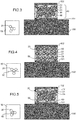
- the capacity as shown on the figure 3 is advantageously intended for low or medium voltage applications. Such a capacity aims, in particular, for a breakdown field of the order of 100 MV / m.
- the dielectric film 40 further comprises electrically insulating nanoparticles 60 ( figures 4 and 5 ).
- electrically insulating is meant an intrinsic electrical resistivity greater than 10 12 ohm.cm.
- the emission of electrons by field effect at the metal / polymer interface leads, at strong fields, to an increase in electrical losses and to heating which risks destroying the capacitor.
- the circulation of these electrons is advantageously blocked by the electrically insulating nanoparticles 60 which form 2D insulating “barriers” (therefore very thin).
- the electrically insulating nanoparticles 60 are arranged across the paths of the conductions (insert of the figures 4 and 5 ). Electrical losses are reduced.
- They may be mineral nanoparticles, for example silica nanoparticles, nanoparticles of complex oxides, for example barium titanate (BaTiO 3 ) or / and strontium (SrTiO 3 ), diamond or carbide nanoparticles. silicon (SiC).
- silica nanoparticles for example silica nanoparticles, nanoparticles of complex oxides, for example barium titanate (BaTiO 3 ) or / and strontium (SrTiO 3 ), diamond or carbide nanoparticles.
- SiC silicon
- tubular or lamellar nanoparticles can be tubular or lamellar nanoparticles.
- tubular or lamellar nanoparticles is understood to mean particles of which one of the dimensions is much smaller than the other two. Such tubular particles or lamellars most often have a thickness e (or a diameter d) much less than their length L or width l.
- the e / L (or d / L) and e / l (or d / l) ratio is less than or equal to 0.5 and preferably less than or equal to 0.1 or to 0.01.
- tubular or lamellar nanoparticles are made of hexagonal boron nitride (h-BN). It can also be graphene oxide GO.
- Lamellar nanoparticles in particular h-BN and GO nanoparticles, can, for example, be exfoliated.
- exfoliated is understood to mean that the lamellae or sheets of the stack forming the lamellar nanoparticles are removed so as to obtain lamellar particles formed from one or a few leaves (2, 3, 4 or 5 for example).
- Ultrasonic exfoliation can produce large amounts.
- Tubular particles in h-BN can, for example, be produced in large quantities by aerosol pyrolysis (spray pyrolysis)
- the dielectric film comprises an alternation of layers of hydrid nanoparticles 20 and of layers of electrically insulating nanoparticles 60 ( figure 4 ).
- the hydrid nanoparticles and the electrically insulating nanoparticles are randomly dispersed in the polymer matrix.
- the electrically insulating nanoparticles 60 are placed in and / or on the shell of the hydride nanoparticles 20.
- This latter embodiment can be combined with the first or the second embodiment.
- electrically insulating nanoparticles 60 dispersed randomly in the polymeric matrix 50 and in the shell of the hybrid nanoparticles 20.
- Such a nanocomposite dielectric film 40 has a high resistivity (for example 10 12 - 10 15 ⁇ Ohm.cm), a dielectric constant which can be exceptionally high (for example 100 or 1000) when approaching the electrical percolation threshold (for example 0.5, 1, or 2% by weight) and a high resistance to electrical breakdown (for example 10 MV / m, 100 MV / m, 500 MV / m).
- a high resistivity for example 10 12 - 10 15 ⁇ Ohm.cm
- a dielectric constant which can be exceptionally high for example 100 or 1000
- the electrical percolation threshold for example 0.5, 1, or 2% by weight
- a high resistance to electrical breakdown for example 10 MV / m, 100 MV / m, 500 MV / m.
- the hybrid nanoparticles 20 are electrically insulated, exhibit a low size distribution and are homogeneously dispersed in the dielectric film. With such nanoparticles 20, it is possible to miniaturize capacitors intended for high voltage applications.
- Such a capacity can be used for the integration of power conversion modules, for example for electric vehicles.
- precursor of the polymer monomers and / or oligomers and / or prepolymers leading to the formation of the polymer.
- the polymer precursor is combined with a polymerization initiator.
- the polymerization initiator is, for example, a photoinitiator or a radical initiator. After shaping, the precursor is polymerized so as to obtain the polymer.
- the solvent is an organic solvent.
- the solvent is evaporated after depositing the solution.
- the solution can be deposited by a contactless deposition technique. It may be, for example, a coating technique, such as curtain coating ("curtain coating” or “flow-coating") or by soaking-shrinkage (“dip-coating”) or else centrifugal coating (“spin-coating”) Preferably, this is centrifugal coating.
- the film can be exposed to a light source, preferably an ultra-violet (UV) source.
- a light source preferably an ultra-violet (UV) source.
- UV ultra-violet
- the film can be hot pressed, preferably in the vicinity of the glass transition temperature.
- the solution of step i) can also contain the electrically insulating nanoparticles 60 as described above.
- the solution containing the hybrid nanoparticles 20 then a second solution containing the electrically insulating nanoparticles 60.
- This second solution can also contain a third polymer material or the precursors of the third polymer material.
- the third polymeric material is preferably identical to the second polymeric material. The two solutions can be deposited alternately until the desired number of layers is obtained.
- the process can be carried out at room temperature (20-25 ° C).
- the process is carried out at ambient pressure (1 bar).
- the process is advantageously carried out in air, there is no need to work in a controlled atmosphere.
- the dielectric film 40 can be obtained by plasma deposition.
- a deposition technique will be chosen, the processing temperature of which is lower than the melting point of the polymer material of the shell.
- the emulsion will make it possible to sort these nanoparticles 20 according to their size. For example, for a powder for which the average diameter of the nanoparticles 20 is of the order of 30 nm, the size dispersion is large and can range from less than 5 nm to more than 300 nm. This is detrimental for the manufacture of a nanocomposite material with controlled properties.
- the emulsion acts as a filter. Nanoparticles of a certain size are selected by appropriately choosing the size of the micelles.
- the size of the micelles is 2 to 3 times greater than the average size of the nanoparticles 20 (for example between 60 and 90 nm for 30 nm). Only the nanoparticles 20 of average size of the order of 30 nm will be trapped in the emulsion and only these nanoparticles 20 will subsequently be coated with a layer of polymer 23. In this way, the larger nanoparticles 20 (for example 100 nm or 300 nm) will form a sediment not coated with polymer which will be easily removed later.
- the small nanoparticles 20 (for example of 10 nm and less) imperfectly covered with carbonaceous coating 22 oxidize rapidly, and therefore more hydrophobic, remain in the organic phase. Nanoparticles in suspension in the organic phase or in the sediment, and do not participate in polymerization.
- a micelle contains a single nanoparticle 20.
- the size of the droplets will be chosen as a function of the size of the nanoparticles 20 and of the thickness of the polymer layer 23 desired.
- step a an aqueous phase and an organic phase are brought together so as to obtain a two-phase mixture, then an emulsification of the two-phase mixture is carried out in the presence of a surfactant (or emulsifier ), whereby a water-in-oil emulsion is formed, formed by droplets of the aqueous phase dispersed in the organic phase.
- a surfactant or emulsifier
- the droplets form micelles (hydrophilic core - hydrophobic tails)
- Emulsification is, for example, formed by stirring (ultrasound).
- the mixture remains stable thanks to the addition of the emulsifier.
- the speed or the kinetics of evolution of the mixture is almost zero, which makes it a particularly stable confined reaction medium and suitable for the synthesis of polymers by polymerization of monomers.
- the emulsion may contain other ingredients, which are not reactive, but which are necessary for stabilizing the emulsion.
- the electrically insulating nanoparticles are added to the emulsion in step a).
- the particles are advantageously hydrophobic so as to be dispersed in the organic phase with the monomers.
- some of these electrically insulating nanoparticles are entrained by the monomers and are found trapped in and / or on the polymer layer coating the metal nanoparticle.
- the polymerization initiator and the monomers, precursors of the polymer are added to the emulsion formed in step b).
- the amounts of initiator and of monomer are chosen so as to obtain a low polymerization yield in order to create a very thin layer 23 of polymer at the surface of the nanoparticles 20 (for example from 5 nm to 10 nm).
- low is meant a polymerization yield of less than 50%, and preferably less than 25%, preferably less than 20%, for example of the order of 10%.
- the amount of monomers consumed is determined by the polymerization yield.
- steps c) and d) are carried out simultaneously.
- the method successively comprises steps c), d) and c).
- step c) is carried out prior to step b).
- the polymerization initiator also called the polymerization initiator
- the polymerization is initiated.
- Polymerization is radical polymerization. This is initiated by the entry into the micelle of an oligo-radical (hydrophilic) previously formed in aqueous phase which will generate a gradual consumption of the (hydrophobic) monomers stored in the dispersing phase (here the oil), until the micelle is saturated.
- the conditions are suitable for reacting the polymerization initiator, typically by raising the temperature and / or by sonication.
- the polymerization is carried out by heating the emulsion to a temperature of 40 ° C to 80 ° C, preferably 50 ° C to 80 ° C, and preferably 60 ° C to 70 ° C. These temperature ranges can be adapted depending on the temperature at which the polymerization initiator becomes reactive.
- the polymerization step generally lasts from a few minutes to a few tens of minutes, for example about 20 minutes. This step can be performed under ultrasound using a sonication probe.
- the droplets of the emulsion are converted into solid elements dispersed in the organic phase.
- dispenser is meant a stable suspension of solid elements, preferably individualized and non-agglomerated, in a continuous liquid phase.
- the elements have an average size equivalent to the average size of the droplets of the emulsion from which they originate.
- a “washing” (precipitation / dilution sequence) is advantageously carried out in order to eliminate the reaction products not consumed and to recover the latex.
- a centrifugation step is advantageously carried out to separate the metal / C / polymer nanoparticles from the polymer beads.
- a ready-to-use composite material (colloid or powder) is obtained.
- Ni / graphene / PS nanoparticles were prepared by a mini-emulsion process. High molecular weight polystyrene (PS) is added to a solution containing these nanoparticles.
- PS High molecular weight polystyrene
- a first gold electrode 101 is formed by vacuum evaporation.
- the solution containing the nanoparticles and the PS is then deposited by spin coating (“spincoating”).
- the thickness of the dielectric film 40 can be adjusted between 0.05 ⁇ m and 50 ⁇ m. It is, for example, 2 ⁇ m for a deposit at 1000 rpm.
- the second electrode 102 is then formed so as to obtain a planar capacitance (2D).
- the capacitor exhibits a statistically homogeneous distribution of size sorted Ni / C / polymer nanoparticles 20 in the host matrix 50 of polystyrene.
Landscapes
- Engineering & Computer Science (AREA)
- Power Engineering (AREA)
- Manufacturing & Machinery (AREA)
- Microelectronics & Electronic Packaging (AREA)
- Chemical & Material Sciences (AREA)
- Inorganic Chemistry (AREA)
- Fixed Capacitors And Capacitor Manufacturing Machines (AREA)
- Compositions Of Macromolecular Compounds (AREA)
- Carbon And Carbon Compounds (AREA)
- Ceramic Capacitors (AREA)
- Health & Medical Sciences (AREA)
- Chemical Kinetics & Catalysis (AREA)
- Medicinal Chemistry (AREA)
- Polymers & Plastics (AREA)
- Organic Chemistry (AREA)
- Materials Engineering (AREA)
Applications Claiming Priority (1)
| Application Number | Priority Date | Filing Date | Title |
|---|---|---|---|
| FR1901600A FR3092930B1 (fr) | 2019-02-18 | 2019-02-18 | Capacite metal-polymere comprenant un film dielectrique a forte constante dielectrique et a fort champ de claquage |
Publications (2)
| Publication Number | Publication Date |
|---|---|
| EP3696834A1 true EP3696834A1 (de) | 2020-08-19 |
| EP3696834B1 EP3696834B1 (de) | 2024-04-03 |
Family
ID=67810664
Family Applications (1)
| Application Number | Title | Priority Date | Filing Date |
|---|---|---|---|
| EP20157469.6A Active EP3696834B1 (de) | 2019-02-18 | 2020-02-14 | Metall-polymer-kapazität, die eine dielektrische folie mit einer starken dielektrischen konstante und einer starken durchbruchfeldstärke umfasst |
Country Status (4)
| Country | Link |
|---|---|
| US (1) | US20200265997A1 (de) |
| EP (1) | EP3696834B1 (de) |
| JP (1) | JP7442336B2 (de) |
| FR (1) | FR3092930B1 (de) |
Cited By (2)
| Publication number | Priority date | Publication date | Assignee | Title |
|---|---|---|---|---|
| CN114121490A (zh) * | 2021-11-25 | 2022-03-01 | 江苏科技大学 | 一种低损耗含氟聚合物多层介质膜、其制备方法及应用 |
| CN116082683A (zh) * | 2023-03-03 | 2023-05-09 | 哈尔滨理工大学 | 一种芴聚酯与聚丙烯酸乙酯-氯乙醚基全有机共混复合材料的制备方法及应用 |
Families Citing this family (6)
| Publication number | Priority date | Publication date | Assignee | Title |
|---|---|---|---|---|
| FR3092833B1 (fr) * | 2019-02-18 | 2021-07-16 | Commissariat Energie Atomique | Procede de fabrication de nanoparticules hybrides metal/polymere a faible distribution de tailles par polymerisation en mini-emulsion |
| CN113527826B (zh) * | 2021-06-04 | 2022-08-26 | 宁波大学 | 一种片状核壳结构掺杂聚偏氟乙烯共聚物的复合薄膜及其制备方法 |
| CN113736195B (zh) * | 2021-09-03 | 2022-04-15 | 武汉理工大学 | 一种耐高温铁电聚合物基介电储能复合薄膜及其制备方法和应用 |
| CN115850544B (zh) * | 2022-12-21 | 2023-10-20 | 浙江工业大学 | Ag@PMMA纳米复合材料、其制备及PVDF基介电复合材料的制备方法 |
| CN117301674A (zh) * | 2023-08-25 | 2023-12-29 | 北京科技大学 | 一种五层复合薄膜及其制备方法和应用 |
| CN117757147B (zh) * | 2023-12-15 | 2024-12-13 | 哈尔滨理工大学 | 一种核壳结构填料及其制备方法和在聚醚酰亚胺基储能复合介质薄膜中的应用 |
Citations (2)
| Publication number | Priority date | Publication date | Assignee | Title |
|---|---|---|---|---|
| US20100123996A1 (en) * | 2008-11-17 | 2010-05-20 | Fujitsu Limited | Structural body, capacitor, and method of fabricating the capacitor |
| EP3252782A1 (de) * | 2016-05-03 | 2017-12-06 | Commissariat à l'Energie Atomique et aux Energies Alternatives | Nanoverbundmaterial und entsprechendes herstellungsverfahren |
Family Cites Families (1)
| Publication number | Priority date | Publication date | Assignee | Title |
|---|---|---|---|---|
| CN105140028A (zh) | 2015-09-25 | 2015-12-09 | 安捷利(番禺)电子实业有限公司 | 一种高介电常数的埋入式电容的制备方法 |
-
2019
- 2019-02-18 FR FR1901600A patent/FR3092930B1/fr active Active
-
2020
- 2020-02-11 US US16/787,071 patent/US20200265997A1/en not_active Abandoned
- 2020-02-14 EP EP20157469.6A patent/EP3696834B1/de active Active
- 2020-02-17 JP JP2020024409A patent/JP7442336B2/ja active Active
Patent Citations (2)
| Publication number | Priority date | Publication date | Assignee | Title |
|---|---|---|---|---|
| US20100123996A1 (en) * | 2008-11-17 | 2010-05-20 | Fujitsu Limited | Structural body, capacitor, and method of fabricating the capacitor |
| EP3252782A1 (de) * | 2016-05-03 | 2017-12-06 | Commissariat à l'Energie Atomique et aux Energies Alternatives | Nanoverbundmaterial und entsprechendes herstellungsverfahren |
Non-Patent Citations (5)
Cited By (3)
| Publication number | Priority date | Publication date | Assignee | Title |
|---|---|---|---|---|
| CN114121490A (zh) * | 2021-11-25 | 2022-03-01 | 江苏科技大学 | 一种低损耗含氟聚合物多层介质膜、其制备方法及应用 |
| CN116082683A (zh) * | 2023-03-03 | 2023-05-09 | 哈尔滨理工大学 | 一种芴聚酯与聚丙烯酸乙酯-氯乙醚基全有机共混复合材料的制备方法及应用 |
| CN116082683B (zh) * | 2023-03-03 | 2023-08-18 | 哈尔滨理工大学 | 一种芴聚酯与聚丙烯酸乙酯-氯乙醚基全有机共混复合材料的制备方法及应用 |
Also Published As
| Publication number | Publication date |
|---|---|
| FR3092930A1 (fr) | 2020-08-21 |
| JP2020136680A (ja) | 2020-08-31 |
| EP3696834B1 (de) | 2024-04-03 |
| FR3092930B1 (fr) | 2021-03-12 |
| JP7442336B2 (ja) | 2024-03-04 |
| US20200265997A1 (en) | 2020-08-20 |
Similar Documents
| Publication | Publication Date | Title |
|---|---|---|
| EP3696834B1 (de) | Metall-polymer-kapazität, die eine dielektrische folie mit einer starken dielektrischen konstante und einer starken durchbruchfeldstärke umfasst | |
| US10355216B2 (en) | Method of selective separation of semiconducting carbon nanotubes, dispersion of semiconducting carbon nanotubes, and electronic device including carbon nanotubes separated by using the method | |
| EP3020050A1 (de) | Elektrisch isolierendes verbundmaterial, verfahren zur herstellung solch eines materials und verwendung davon als elektrisches isolationsmittel | |
| EP3252782B1 (de) | Nanoverbundmaterial und entsprechendes herstellungsverfahren | |
| FR2953824A1 (fr) | Materiau solide composite piezoelectrique et/ou pyroelectrique, procede d'obtention et utilisation d'un tel materiau | |
| EP3696203B1 (de) | Herstellungsverfahren von hybriden metall-/polymer-nanopartikeln mit geringer grössenverteilung durch polymerisation in mini-emulsionen | |
| Dizayee et al. | Synergistic effect of Ni (OH) 2 and MXene nanosheets in 3D framework on the improvement of dielectric, energy storage, mechanical and thermal characteristics of polyvinylidene fluoride (PVDF) polymeric composites | |
| Che et al. | Inkjet printing of all aqueous inks to flexible microcapacitors for high‐energy storage | |
| KR20160020410A (ko) | 고점도 알콜 용매 및 실리콘/게르마늄계 나노입자를 포함하는 인쇄용 잉크 | |
| US8790773B2 (en) | Tailorable dielectric material with complex permittivity characteristics | |
| FR3057873A1 (fr) | Materiau composite electriquement et thermiquement conducteur | |
| KR101618975B1 (ko) | 그래핀 나노시트의 제조방법 | |
| EP4035661B1 (de) | Verfahren zur herstellung eines verbundmaterials, das ein polymer und nanomaterialien umfasst | |
| US9444003B2 (en) | Layer-by-layer nanoassembled nanoparticles based thin films for solar cell and other applications | |
| FR3052908A1 (fr) | Cable electrique comprenant une couche metallique | |
| CN101916825A (zh) | 一种聚合物基的纳米晶存储器电容及其制作方法 | |
| JP5969905B2 (ja) | 薄層黒鉛または薄層黒鉛化合物の配向膜の製造方法 | |
| KR102151393B1 (ko) | 산화그래핀의 분급 방법 및 그에 의해 분급된 산화그래핀 | |
| Chi et al. | Enhanced Energy Storage Properties of PVDF-HFP Composites by Introducing ZnO@ ZnS Heterojunction: H. Chi et al | |
| Zhang et al. | Scalable Production of Two-Dimensional Materials and Its Reliable Resistive Switching | |
| Gackowski et al. | Enhancing energy density in thin-film nanocomposite dielectric capacitors through surface functionalization of nanoparticles | |
| US12239008B2 (en) | Carbon nanotube monolayer film, method of preparing the same, and electronic device including the same | |
| EP3312226A1 (de) | Material zur verteilung eines elektrischen felds, sein herstellungsverfahren und vorrichtung, die ein solches material umfasst | |
| Che et al. | Charge-Neutralized Colloids for Waterborne High-Energy Dielectrics | |
| Nikolaeva et al. | Conducting properties of single-wall carbon nanotubes in composites based on polystyrene |
Legal Events
| Date | Code | Title | Description |
|---|---|---|---|
| PUAI | Public reference made under article 153(3) epc to a published international application that has entered the european phase |
Free format text: ORIGINAL CODE: 0009012 |
|
| STAA | Information on the status of an ep patent application or granted ep patent |
Free format text: STATUS: REQUEST FOR EXAMINATION WAS MADE |
|
| 17P | Request for examination filed |
Effective date: 20200214 |
|
| AK | Designated contracting states |
Kind code of ref document: A1 Designated state(s): AL AT BE BG CH CY CZ DE DK EE ES FI FR GB GR HR HU IE IS IT LI LT LU LV MC MK MT NL NO PL PT RO RS SE SI SK SM TR |
|
| AX | Request for extension of the european patent |
Extension state: BA ME |
|
| GRAP | Despatch of communication of intention to grant a patent |
Free format text: ORIGINAL CODE: EPIDOSNIGR1 |
|
| STAA | Information on the status of an ep patent application or granted ep patent |
Free format text: STATUS: GRANT OF PATENT IS INTENDED |
|
| INTG | Intention to grant announced |
Effective date: 20231016 |
|
| GRAS | Grant fee paid |
Free format text: ORIGINAL CODE: EPIDOSNIGR3 |
|
| GRAA | (expected) grant |
Free format text: ORIGINAL CODE: 0009210 |
|
| STAA | Information on the status of an ep patent application or granted ep patent |
Free format text: STATUS: THE PATENT HAS BEEN GRANTED |
|
| AK | Designated contracting states |
Kind code of ref document: B1 Designated state(s): AL AT BE BG CH CY CZ DE DK EE ES FI FR GB GR HR HU IE IS IT LI LT LU LV MC MK MT NL NO PL PT RO RS SE SI SK SM TR |
|
| REG | Reference to a national code |
Ref country code: CH Ref legal event code: EP |
|
| REG | Reference to a national code |
Ref country code: IE Ref legal event code: FG4D Free format text: LANGUAGE OF EP DOCUMENT: FRENCH |
|
| REG | Reference to a national code |
Ref country code: DE Ref legal event code: R096 Ref document number: 602020028166 Country of ref document: DE |
|
| REG | Reference to a national code |
Ref country code: LT Ref legal event code: MG9D |
|
| REG | Reference to a national code |
Ref country code: NL Ref legal event code: MP Effective date: 20240403 |
|
| REG | Reference to a national code |
Ref country code: AT Ref legal event code: MK05 Ref document number: 1673314 Country of ref document: AT Kind code of ref document: T Effective date: 20240403 |
|
| PG25 | Lapsed in a contracting state [announced via postgrant information from national office to epo] |
Ref country code: NL Free format text: LAPSE BECAUSE OF FAILURE TO SUBMIT A TRANSLATION OF THE DESCRIPTION OR TO PAY THE FEE WITHIN THE PRESCRIBED TIME-LIMIT Effective date: 20240403 |
|
| PG25 | Lapsed in a contracting state [announced via postgrant information from national office to epo] |
Ref country code: NL Free format text: LAPSE BECAUSE OF FAILURE TO SUBMIT A TRANSLATION OF THE DESCRIPTION OR TO PAY THE FEE WITHIN THE PRESCRIBED TIME-LIMIT Effective date: 20240403 |
|
| PG25 | Lapsed in a contracting state [announced via postgrant information from national office to epo] |
Ref country code: IS Free format text: LAPSE BECAUSE OF FAILURE TO SUBMIT A TRANSLATION OF THE DESCRIPTION OR TO PAY THE FEE WITHIN THE PRESCRIBED TIME-LIMIT Effective date: 20240803 |
|
| PG25 | Lapsed in a contracting state [announced via postgrant information from national office to epo] |
Ref country code: BG Free format text: LAPSE BECAUSE OF FAILURE TO SUBMIT A TRANSLATION OF THE DESCRIPTION OR TO PAY THE FEE WITHIN THE PRESCRIBED TIME-LIMIT Effective date: 20240403 |
|
| PG25 | Lapsed in a contracting state [announced via postgrant information from national office to epo] |
Ref country code: HR Free format text: LAPSE BECAUSE OF FAILURE TO SUBMIT A TRANSLATION OF THE DESCRIPTION OR TO PAY THE FEE WITHIN THE PRESCRIBED TIME-LIMIT Effective date: 20240403 Ref country code: FI Free format text: LAPSE BECAUSE OF FAILURE TO SUBMIT A TRANSLATION OF THE DESCRIPTION OR TO PAY THE FEE WITHIN THE PRESCRIBED TIME-LIMIT Effective date: 20240403 |
|
| PG25 | Lapsed in a contracting state [announced via postgrant information from national office to epo] |
Ref country code: GR Free format text: LAPSE BECAUSE OF FAILURE TO SUBMIT A TRANSLATION OF THE DESCRIPTION OR TO PAY THE FEE WITHIN THE PRESCRIBED TIME-LIMIT Effective date: 20240704 |
|
| PG25 | Lapsed in a contracting state [announced via postgrant information from national office to epo] |
Ref country code: PT Free format text: LAPSE BECAUSE OF FAILURE TO SUBMIT A TRANSLATION OF THE DESCRIPTION OR TO PAY THE FEE WITHIN THE PRESCRIBED TIME-LIMIT Effective date: 20240805 |
|
| PG25 | Lapsed in a contracting state [announced via postgrant information from national office to epo] |
Ref country code: ES Free format text: LAPSE BECAUSE OF FAILURE TO SUBMIT A TRANSLATION OF THE DESCRIPTION OR TO PAY THE FEE WITHIN THE PRESCRIBED TIME-LIMIT Effective date: 20240403 |
|
| PG25 | Lapsed in a contracting state [announced via postgrant information from national office to epo] |
Ref country code: CZ Free format text: LAPSE BECAUSE OF FAILURE TO SUBMIT A TRANSLATION OF THE DESCRIPTION OR TO PAY THE FEE WITHIN THE PRESCRIBED TIME-LIMIT Effective date: 20240403 |
|
| PG25 | Lapsed in a contracting state [announced via postgrant information from national office to epo] |
Ref country code: AT Free format text: LAPSE BECAUSE OF FAILURE TO SUBMIT A TRANSLATION OF THE DESCRIPTION OR TO PAY THE FEE WITHIN THE PRESCRIBED TIME-LIMIT Effective date: 20240403 |
|
| PG25 | Lapsed in a contracting state [announced via postgrant information from national office to epo] |
Ref country code: PL Free format text: LAPSE BECAUSE OF FAILURE TO SUBMIT A TRANSLATION OF THE DESCRIPTION OR TO PAY THE FEE WITHIN THE PRESCRIBED TIME-LIMIT Effective date: 20240403 |
|
| PG25 | Lapsed in a contracting state [announced via postgrant information from national office to epo] |
Ref country code: LV Free format text: LAPSE BECAUSE OF FAILURE TO SUBMIT A TRANSLATION OF THE DESCRIPTION OR TO PAY THE FEE WITHIN THE PRESCRIBED TIME-LIMIT Effective date: 20240403 |
|
| RAP4 | Party data changed (patent owner data changed or rights of a patent transferred) |
Owner name: COMMISSARIAT A L'ENERGIE ATOMIQUE ET AUX ENERGIESALTERNATIVES |
|
| PG25 | Lapsed in a contracting state [announced via postgrant information from national office to epo] |
Ref country code: PT Free format text: LAPSE BECAUSE OF FAILURE TO SUBMIT A TRANSLATION OF THE DESCRIPTION OR TO PAY THE FEE WITHIN THE PRESCRIBED TIME-LIMIT Effective date: 20240805 Ref country code: PL Free format text: LAPSE BECAUSE OF FAILURE TO SUBMIT A TRANSLATION OF THE DESCRIPTION OR TO PAY THE FEE WITHIN THE PRESCRIBED TIME-LIMIT Effective date: 20240403 Ref country code: NO Free format text: LAPSE BECAUSE OF FAILURE TO SUBMIT A TRANSLATION OF THE DESCRIPTION OR TO PAY THE FEE WITHIN THE PRESCRIBED TIME-LIMIT Effective date: 20240703 Ref country code: LV Free format text: LAPSE BECAUSE OF FAILURE TO SUBMIT A TRANSLATION OF THE DESCRIPTION OR TO PAY THE FEE WITHIN THE PRESCRIBED TIME-LIMIT Effective date: 20240403 Ref country code: IS Free format text: LAPSE BECAUSE OF FAILURE TO SUBMIT A TRANSLATION OF THE DESCRIPTION OR TO PAY THE FEE WITHIN THE PRESCRIBED TIME-LIMIT Effective date: 20240803 Ref country code: HR Free format text: LAPSE BECAUSE OF FAILURE TO SUBMIT A TRANSLATION OF THE DESCRIPTION OR TO PAY THE FEE WITHIN THE PRESCRIBED TIME-LIMIT Effective date: 20240403 Ref country code: GR Free format text: LAPSE BECAUSE OF FAILURE TO SUBMIT A TRANSLATION OF THE DESCRIPTION OR TO PAY THE FEE WITHIN THE PRESCRIBED TIME-LIMIT Effective date: 20240704 Ref country code: FI Free format text: LAPSE BECAUSE OF FAILURE TO SUBMIT A TRANSLATION OF THE DESCRIPTION OR TO PAY THE FEE WITHIN THE PRESCRIBED TIME-LIMIT Effective date: 20240403 Ref country code: ES Free format text: LAPSE BECAUSE OF FAILURE TO SUBMIT A TRANSLATION OF THE DESCRIPTION OR TO PAY THE FEE WITHIN THE PRESCRIBED TIME-LIMIT Effective date: 20240403 Ref country code: CZ Free format text: LAPSE BECAUSE OF FAILURE TO SUBMIT A TRANSLATION OF THE DESCRIPTION OR TO PAY THE FEE WITHIN THE PRESCRIBED TIME-LIMIT Effective date: 20240403 Ref country code: BG Free format text: LAPSE BECAUSE OF FAILURE TO SUBMIT A TRANSLATION OF THE DESCRIPTION OR TO PAY THE FEE WITHIN THE PRESCRIBED TIME-LIMIT Effective date: 20240403 Ref country code: AT Free format text: LAPSE BECAUSE OF FAILURE TO SUBMIT A TRANSLATION OF THE DESCRIPTION OR TO PAY THE FEE WITHIN THE PRESCRIBED TIME-LIMIT Effective date: 20240403 Ref country code: RS Free format text: LAPSE BECAUSE OF FAILURE TO SUBMIT A TRANSLATION OF THE DESCRIPTION OR TO PAY THE FEE WITHIN THE PRESCRIBED TIME-LIMIT Effective date: 20240703 |
|
| REG | Reference to a national code |
Ref country code: DE Ref legal event code: R097 Ref document number: 602020028166 Country of ref document: DE |
|
| PG25 | Lapsed in a contracting state [announced via postgrant information from national office to epo] |
Ref country code: DK Free format text: LAPSE BECAUSE OF FAILURE TO SUBMIT A TRANSLATION OF THE DESCRIPTION OR TO PAY THE FEE WITHIN THE PRESCRIBED TIME-LIMIT Effective date: 20240403 |
|
| PG25 | Lapsed in a contracting state [announced via postgrant information from national office to epo] |
Ref country code: EE Free format text: LAPSE BECAUSE OF FAILURE TO SUBMIT A TRANSLATION OF THE DESCRIPTION OR TO PAY THE FEE WITHIN THE PRESCRIBED TIME-LIMIT Effective date: 20240403 |
|
| PG25 | Lapsed in a contracting state [announced via postgrant information from national office to epo] |
Ref country code: SK Free format text: LAPSE BECAUSE OF FAILURE TO SUBMIT A TRANSLATION OF THE DESCRIPTION OR TO PAY THE FEE WITHIN THE PRESCRIBED TIME-LIMIT Effective date: 20240403 Ref country code: RO Free format text: LAPSE BECAUSE OF FAILURE TO SUBMIT A TRANSLATION OF THE DESCRIPTION OR TO PAY THE FEE WITHIN THE PRESCRIBED TIME-LIMIT Effective date: 20240403 |
|
| PG25 | Lapsed in a contracting state [announced via postgrant information from national office to epo] |
Ref country code: SM Free format text: LAPSE BECAUSE OF FAILURE TO SUBMIT A TRANSLATION OF THE DESCRIPTION OR TO PAY THE FEE WITHIN THE PRESCRIBED TIME-LIMIT Effective date: 20240403 |
|
| PG25 | Lapsed in a contracting state [announced via postgrant information from national office to epo] |
Ref country code: SM Free format text: LAPSE BECAUSE OF FAILURE TO SUBMIT A TRANSLATION OF THE DESCRIPTION OR TO PAY THE FEE WITHIN THE PRESCRIBED TIME-LIMIT Effective date: 20240403 Ref country code: SK Free format text: LAPSE BECAUSE OF FAILURE TO SUBMIT A TRANSLATION OF THE DESCRIPTION OR TO PAY THE FEE WITHIN THE PRESCRIBED TIME-LIMIT Effective date: 20240403 Ref country code: RO Free format text: LAPSE BECAUSE OF FAILURE TO SUBMIT A TRANSLATION OF THE DESCRIPTION OR TO PAY THE FEE WITHIN THE PRESCRIBED TIME-LIMIT Effective date: 20240403 Ref country code: EE Free format text: LAPSE BECAUSE OF FAILURE TO SUBMIT A TRANSLATION OF THE DESCRIPTION OR TO PAY THE FEE WITHIN THE PRESCRIBED TIME-LIMIT Effective date: 20240403 Ref country code: DK Free format text: LAPSE BECAUSE OF FAILURE TO SUBMIT A TRANSLATION OF THE DESCRIPTION OR TO PAY THE FEE WITHIN THE PRESCRIBED TIME-LIMIT Effective date: 20240403 |
|
| PLBE | No opposition filed within time limit |
Free format text: ORIGINAL CODE: 0009261 |
|
| STAA | Information on the status of an ep patent application or granted ep patent |
Free format text: STATUS: NO OPPOSITION FILED WITHIN TIME LIMIT |
|
| 26N | No opposition filed |
Effective date: 20250106 |
|
| PG25 | Lapsed in a contracting state [announced via postgrant information from national office to epo] |
Ref country code: SI Free format text: LAPSE BECAUSE OF FAILURE TO SUBMIT A TRANSLATION OF THE DESCRIPTION OR TO PAY THE FEE WITHIN THE PRESCRIBED TIME-LIMIT Effective date: 20240403 |
|
| PG25 | Lapsed in a contracting state [announced via postgrant information from national office to epo] |
Ref country code: SE Free format text: LAPSE BECAUSE OF FAILURE TO SUBMIT A TRANSLATION OF THE DESCRIPTION OR TO PAY THE FEE WITHIN THE PRESCRIBED TIME-LIMIT Effective date: 20240403 |
|
| PG25 | Lapsed in a contracting state [announced via postgrant information from national office to epo] |
Ref country code: MC Free format text: LAPSE BECAUSE OF FAILURE TO SUBMIT A TRANSLATION OF THE DESCRIPTION OR TO PAY THE FEE WITHIN THE PRESCRIBED TIME-LIMIT Effective date: 20240403 |
|
| REG | Reference to a national code |
Ref country code: CH Ref legal event code: PL |
|
| PG25 | Lapsed in a contracting state [announced via postgrant information from national office to epo] |
Ref country code: LU Free format text: LAPSE BECAUSE OF NON-PAYMENT OF DUE FEES Effective date: 20250214 |
|
| PG25 | Lapsed in a contracting state [announced via postgrant information from national office to epo] |
Ref country code: CH Free format text: LAPSE BECAUSE OF NON-PAYMENT OF DUE FEES Effective date: 20250228 |
|
| REG | Reference to a national code |
Ref country code: BE Ref legal event code: MM Effective date: 20250228 |
|
| PG25 | Lapsed in a contracting state [announced via postgrant information from national office to epo] |
Ref country code: BE Free format text: LAPSE BECAUSE OF NON-PAYMENT OF DUE FEES Effective date: 20250228 |
|
| PG25 | Lapsed in a contracting state [announced via postgrant information from national office to epo] |
Ref country code: IE Free format text: LAPSE BECAUSE OF NON-PAYMENT OF DUE FEES Effective date: 20250214 |
|
| PG25 | Lapsed in a contracting state [announced via postgrant information from national office to epo] |
Ref country code: IT Free format text: LAPSE BECAUSE OF FAILURE TO SUBMIT A TRANSLATION OF THE DESCRIPTION OR TO PAY THE FEE WITHIN THE PRESCRIBED TIME-LIMIT Effective date: 20240403 |
|
| PGFP | Annual fee paid to national office [announced via postgrant information from national office to epo] |
Ref country code: GB Payment date: 20260218 Year of fee payment: 7 |
|
| PGFP | Annual fee paid to national office [announced via postgrant information from national office to epo] |
Ref country code: DE Payment date: 20260217 Year of fee payment: 7 |
|
| PGFP | Annual fee paid to national office [announced via postgrant information from national office to epo] |
Ref country code: FR Payment date: 20260219 Year of fee payment: 7 |