EP3703200A2 - Wafer à laser semi-conducteur et laser semi-conducteur - Google Patents
Wafer à laser semi-conducteur et laser semi-conducteur Download PDFInfo
- Publication number
- EP3703200A2 EP3703200A2 EP20158198.0A EP20158198A EP3703200A2 EP 3703200 A2 EP3703200 A2 EP 3703200A2 EP 20158198 A EP20158198 A EP 20158198A EP 3703200 A2 EP3703200 A2 EP 3703200A2
- Authority
- EP
- European Patent Office
- Prior art keywords
- layer
- semiconductor
- film
- compound semiconductor
- active layer
- Prior art date
- Legal status (The legal status is an assumption and is not a legal conclusion. Google has not performed a legal analysis and makes no representation as to the accuracy of the status listed.)
- Granted
Links
Images

Classifications
-
- H—ELECTRICITY
- H01—ELECTRIC ELEMENTS
- H01S—DEVICES USING THE PROCESS OF LIGHT AMPLIFICATION BY STIMULATED EMISSION OF RADIATION [LASER] TO AMPLIFY OR GENERATE LIGHT; DEVICES USING STIMULATED EMISSION OF ELECTROMAGNETIC RADIATION IN WAVE RANGES OTHER THAN OPTICAL
- H01S5/00—Semiconductor lasers
- H01S5/30—Structure or shape of the active region; Materials used for the active region
- H01S5/34—Structure or shape of the active region; Materials used for the active region comprising quantum well or superlattice structures, e.g. single quantum well [SQW] lasers, multiple quantum well [MQW] lasers or graded index separate confinement heterostructure [GRINSCH] lasers
- H01S5/3401—Structure or shape of the active region; Materials used for the active region comprising quantum well or superlattice structures, e.g. single quantum well [SQW] lasers, multiple quantum well [MQW] lasers or graded index separate confinement heterostructure [GRINSCH] lasers having no PN junction, e.g. unipolar lasers, intersubband lasers, quantum cascade lasers
- H01S5/3402—Structure or shape of the active region; Materials used for the active region comprising quantum well or superlattice structures, e.g. single quantum well [SQW] lasers, multiple quantum well [MQW] lasers or graded index separate confinement heterostructure [GRINSCH] lasers having no PN junction, e.g. unipolar lasers, intersubband lasers, quantum cascade lasers intersubband lasers, e.g. transitions within the conduction or valence bands
-
- H—ELECTRICITY
- H01—ELECTRIC ELEMENTS
- H01S—DEVICES USING THE PROCESS OF LIGHT AMPLIFICATION BY STIMULATED EMISSION OF RADIATION [LASER] TO AMPLIFY OR GENERATE LIGHT; DEVICES USING STIMULATED EMISSION OF ELECTROMAGNETIC RADIATION IN WAVE RANGES OTHER THAN OPTICAL
- H01S5/00—Semiconductor lasers
- H01S5/30—Structure or shape of the active region; Materials used for the active region
- H01S5/34—Structure or shape of the active region; Materials used for the active region comprising quantum well or superlattice structures, e.g. single quantum well [SQW] lasers, multiple quantum well [MQW] lasers or graded index separate confinement heterostructure [GRINSCH] lasers
- H01S5/3401—Structure or shape of the active region; Materials used for the active region comprising quantum well or superlattice structures, e.g. single quantum well [SQW] lasers, multiple quantum well [MQW] lasers or graded index separate confinement heterostructure [GRINSCH] lasers having no PN junction, e.g. unipolar lasers, intersubband lasers, quantum cascade lasers
-
- H—ELECTRICITY
- H01—ELECTRIC ELEMENTS
- H01S—DEVICES USING THE PROCESS OF LIGHT AMPLIFICATION BY STIMULATED EMISSION OF RADIATION [LASER] TO AMPLIFY OR GENERATE LIGHT; DEVICES USING STIMULATED EMISSION OF ELECTROMAGNETIC RADIATION IN WAVE RANGES OTHER THAN OPTICAL
- H01S5/00—Semiconductor lasers
- H01S5/0014—Measuring characteristics or properties thereof
- H01S5/0042—On wafer testing, e.g. lasers are tested before separating wafer into chips
-
- H—ELECTRICITY
- H01—ELECTRIC ELEMENTS
- H01S—DEVICES USING THE PROCESS OF LIGHT AMPLIFICATION BY STIMULATED EMISSION OF RADIATION [LASER] TO AMPLIFY OR GENERATE LIGHT; DEVICES USING STIMULATED EMISSION OF ELECTROMAGNETIC RADIATION IN WAVE RANGES OTHER THAN OPTICAL
- H01S5/00—Semiconductor lasers
- H01S5/20—Structure or shape of the semiconductor body to guide the optical wave ; Confining structures perpendicular to the optical axis, e.g. index or gain guiding, stripe geometry, broad area lasers, gain tailoring, transverse or lateral reflectors, special cladding structures, MQW barrier reflection layers
- H01S5/22—Structure or shape of the semiconductor body to guide the optical wave ; Confining structures perpendicular to the optical axis, e.g. index or gain guiding, stripe geometry, broad area lasers, gain tailoring, transverse or lateral reflectors, special cladding structures, MQW barrier reflection layers having a ridge or stripe structure
-
- H—ELECTRICITY
- H01—ELECTRIC ELEMENTS
- H01S—DEVICES USING THE PROCESS OF LIGHT AMPLIFICATION BY STIMULATED EMISSION OF RADIATION [LASER] TO AMPLIFY OR GENERATE LIGHT; DEVICES USING STIMULATED EMISSION OF ELECTROMAGNETIC RADIATION IN WAVE RANGES OTHER THAN OPTICAL
- H01S5/00—Semiconductor lasers
- H01S5/30—Structure or shape of the active region; Materials used for the active region
- H01S5/34—Structure or shape of the active region; Materials used for the active region comprising quantum well or superlattice structures, e.g. single quantum well [SQW] lasers, multiple quantum well [MQW] lasers or graded index separate confinement heterostructure [GRINSCH] lasers
- H01S5/3418—Structure or shape of the active region; Materials used for the active region comprising quantum well or superlattice structures, e.g. single quantum well [SQW] lasers, multiple quantum well [MQW] lasers or graded index separate confinement heterostructure [GRINSCH] lasers using transitions from higher quantum levels
- H01S5/3419—Structure or shape of the active region; Materials used for the active region comprising quantum well or superlattice structures, e.g. single quantum well [SQW] lasers, multiple quantum well [MQW] lasers or graded index separate confinement heterostructure [GRINSCH] lasers using transitions from higher quantum levels intersubband lasers, e.g. laser transitions within the conduction or valence bands in non unipolar structures
-
- H—ELECTRICITY
- H01—ELECTRIC ELEMENTS
- H01S—DEVICES USING THE PROCESS OF LIGHT AMPLIFICATION BY STIMULATED EMISSION OF RADIATION [LASER] TO AMPLIFY OR GENERATE LIGHT; DEVICES USING STIMULATED EMISSION OF ELECTROMAGNETIC RADIATION IN WAVE RANGES OTHER THAN OPTICAL
- H01S5/00—Semiconductor lasers
- H01S5/30—Structure or shape of the active region; Materials used for the active region
- H01S5/34—Structure or shape of the active region; Materials used for the active region comprising quantum well or superlattice structures, e.g. single quantum well [SQW] lasers, multiple quantum well [MQW] lasers or graded index separate confinement heterostructure [GRINSCH] lasers
- H01S5/343—Structure or shape of the active region; Materials used for the active region comprising quantum well or superlattice structures, e.g. single quantum well [SQW] lasers, multiple quantum well [MQW] lasers or graded index separate confinement heterostructure [GRINSCH] lasers in AIIIBV compounds, e.g. AlGaAs-laser, InP-based laser
-
- H—ELECTRICITY
- H01—ELECTRIC ELEMENTS
- H01S—DEVICES USING THE PROCESS OF LIGHT AMPLIFICATION BY STIMULATED EMISSION OF RADIATION [LASER] TO AMPLIFY OR GENERATE LIGHT; DEVICES USING STIMULATED EMISSION OF ELECTROMAGNETIC RADIATION IN WAVE RANGES OTHER THAN OPTICAL
- H01S5/00—Semiconductor lasers
- H01S5/30—Structure or shape of the active region; Materials used for the active region
- H01S5/34—Structure or shape of the active region; Materials used for the active region comprising quantum well or superlattice structures, e.g. single quantum well [SQW] lasers, multiple quantum well [MQW] lasers or graded index separate confinement heterostructure [GRINSCH] lasers
- H01S5/343—Structure or shape of the active region; Materials used for the active region comprising quantum well or superlattice structures, e.g. single quantum well [SQW] lasers, multiple quantum well [MQW] lasers or graded index separate confinement heterostructure [GRINSCH] lasers in AIIIBV compounds, e.g. AlGaAs-laser, InP-based laser
- H01S5/34306—Structure or shape of the active region; Materials used for the active region comprising quantum well or superlattice structures, e.g. single quantum well [SQW] lasers, multiple quantum well [MQW] lasers or graded index separate confinement heterostructure [GRINSCH] lasers in AIIIBV compounds, e.g. AlGaAs-laser, InP-based laser emitting light at a wavelength longer than 1000nm, e.g. InP based 1300 and 1500nm lasers
-
- H—ELECTRICITY
- H01—ELECTRIC ELEMENTS
- H01S—DEVICES USING THE PROCESS OF LIGHT AMPLIFICATION BY STIMULATED EMISSION OF RADIATION [LASER] TO AMPLIFY OR GENERATE LIGHT; DEVICES USING STIMULATED EMISSION OF ELECTROMAGNETIC RADIATION IN WAVE RANGES OTHER THAN OPTICAL
- H01S5/00—Semiconductor lasers
- H01S5/30—Structure or shape of the active region; Materials used for the active region
- H01S5/34—Structure or shape of the active region; Materials used for the active region comprising quantum well or superlattice structures, e.g. single quantum well [SQW] lasers, multiple quantum well [MQW] lasers or graded index separate confinement heterostructure [GRINSCH] lasers
- H01S5/343—Structure or shape of the active region; Materials used for the active region comprising quantum well or superlattice structures, e.g. single quantum well [SQW] lasers, multiple quantum well [MQW] lasers or graded index separate confinement heterostructure [GRINSCH] lasers in AIIIBV compounds, e.g. AlGaAs-laser, InP-based laser
- H01S5/34346—Structure or shape of the active region; Materials used for the active region comprising quantum well or superlattice structures, e.g. single quantum well [SQW] lasers, multiple quantum well [MQW] lasers or graded index separate confinement heterostructure [GRINSCH] lasers in AIIIBV compounds, e.g. AlGaAs-laser, InP-based laser characterised by the materials of the barrier layers
-
- H—ELECTRICITY
- H01—ELECTRIC ELEMENTS
- H01S—DEVICES USING THE PROCESS OF LIGHT AMPLIFICATION BY STIMULATED EMISSION OF RADIATION [LASER] TO AMPLIFY OR GENERATE LIGHT; DEVICES USING STIMULATED EMISSION OF ELECTROMAGNETIC RADIATION IN WAVE RANGES OTHER THAN OPTICAL
- H01S2301/00—Functional characteristics
- H01S2301/17—Semiconductor lasers comprising special layers
-
- H—ELECTRICITY
- H01—ELECTRIC ELEMENTS
- H01S—DEVICES USING THE PROCESS OF LIGHT AMPLIFICATION BY STIMULATED EMISSION OF RADIATION [LASER] TO AMPLIFY OR GENERATE LIGHT; DEVICES USING STIMULATED EMISSION OF ELECTROMAGNETIC RADIATION IN WAVE RANGES OTHER THAN OPTICAL
- H01S2304/00—Special growth methods for semiconductor lasers
-
- H—ELECTRICITY
- H01—ELECTRIC ELEMENTS
- H01S—DEVICES USING THE PROCESS OF LIGHT AMPLIFICATION BY STIMULATED EMISSION OF RADIATION [LASER] TO AMPLIFY OR GENERATE LIGHT; DEVICES USING STIMULATED EMISSION OF ELECTROMAGNETIC RADIATION IN WAVE RANGES OTHER THAN OPTICAL
- H01S5/00—Semiconductor lasers
- H01S5/30—Structure or shape of the active region; Materials used for the active region
- H01S5/34—Structure or shape of the active region; Materials used for the active region comprising quantum well or superlattice structures, e.g. single quantum well [SQW] lasers, multiple quantum well [MQW] lasers or graded index separate confinement heterostructure [GRINSCH] lasers
- H01S5/343—Structure or shape of the active region; Materials used for the active region comprising quantum well or superlattice structures, e.g. single quantum well [SQW] lasers, multiple quantum well [MQW] lasers or graded index separate confinement heterostructure [GRINSCH] lasers in AIIIBV compounds, e.g. AlGaAs-laser, InP-based laser
- H01S5/34313—Structure or shape of the active region; Materials used for the active region comprising quantum well or superlattice structures, e.g. single quantum well [SQW] lasers, multiple quantum well [MQW] lasers or graded index separate confinement heterostructure [GRINSCH] lasers in AIIIBV compounds, e.g. AlGaAs-laser, InP-based laser with a well layer having only As as V-compound, e.g. AlGaAs, InGaAs
Definitions
- Embodiments described herein relate generally to a semiconductor laser wafer and a semiconductor laser.
- a semiconductor laser that emits infrared includes an active layer in which multiple multi-quantum well structures are stacked.
- composition ratios and the thicknesses of the compound semiconductors included in a well layer and a barrier layer are affected by external disturbances (source material flux, fluctuation of the degree of vacuum, etc.) in the epitaxial crystal growth process. Also, as the number of cascade connection periods of the unit multi-quantum well structure increases, the crystal growth time of the active layer lengthens; and the effects of the external disturbances increase even more.
- a semiconductor laser wafer includes a substrate, a first semiconductor layer, an active layer, a second semiconductor layer, and a composition evaluation layer.
- the first semiconductor layer is provided on the substrate.
- the active layer is provided on the first semiconductor layer; multiple periods of pairs of a light-emitting multi-quantum well region and an injection multi-quantum well region are stacked in the active layer; the light-emitting multi-quantum well region is made of a first compound semiconductor and a second compound semiconductor; and the injection multi-quantum well region is made of the first compound semiconductor and the second compound semiconductor.
- the second semiconductor layer is provided on the active layer.
- the composition evaluation layer is provided above the active layer and includes a first film and a second film; the first film is made of the first compound semiconductor and has a first thickness; and the second film is made of the second compound semiconductor and has a second thickness.
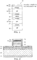
- FIG. 1 is a schematic cross-sectional view of one chip of a semiconductor laser wafer according to a first embodiment of the invention.
- the semiconductor laser wafer 10 includes a substrate 20, a first semiconductor layer 30, an active layer 40, a second semiconductor layer 50, and a composition evaluation layer 60.
- the first semiconductor layer 30 may include, for example, a first contact layer 31, a first cladding layer 32, a first light guide layer 33, etc., in this order on the substrate 20.
- the second semiconductor layer 50 may include, for example, a second light guide layer 51, a second cladding layer 52, a second contact layer 53, etc., in this order on the active layer 40.
- the active layer 40 is provided on the first semiconductor layer 30. Multiple periods of pairs of a light-emitting multi-quantum well region and an injection multi-quantum well region are stacked in the active layer 40; the light-emitting multi-quantum well region is made of a first compound semiconductor and a second compound semiconductor; and the injection multi-quantum well region is made of the first compound semiconductor and the second compound semiconductor.
- the composition evaluation layer 60 is provided on the second semiconductor layer 50 and includes a first film 61 and a second film 62; the first film 61 is made of the first compound semiconductor and has a first thickness; and the second film 62 is made of a mixed crystal of the second compound semiconductor and has a second thickness.
- the first compound semiconductor and the second compound semiconductor each may be, for example, ternary compound mixed crystals.
- the semiconductor laser is a quantum cascade laser (QCL) in which the carrier is an electron
- the polarities of the first semiconductor layer 30 and the second semiconductor layer 50 are set to the n-type.
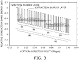
- FIG. 2 is a schematic cross-sectional view of the semiconductor laser according to the first embodiment.
- a stacked body that includes the first semiconductor layer 30, the active layer 40, the second semiconductor layer 50, and the composition evaluation layer 60 and is epitaxially grown on the substrate 20 is patterned into a mesa configuration.
- the mesa-shaped stacked body is included in a ridge waveguide.
- the dug out depth of the mesa reaches partway through the first light guide layer 33 of the first semiconductor layer 30 provided to be adjacent to the active layer 40.
- the dug out depth of the mesa is not limited to FIG. 2 and may reach partway through the first cladding layer 32 provided below the first light guide layer 33, may reach the lower surface of the active layer 40, or may reach the lower surface of the first semiconductor layer 30.
- An insulating film 70 that includes a silicon oxide film and/or a silicon nitride film is provided on the side surface of the ridge waveguide and on the bottom surface exposed at the two sides of the ridge waveguide.
- An upper electrode 72 is provided on the upper surface of the ridge waveguide (the front surface of the second film 62); and a lower electrode 73 is provided on the back surface of the substrate 20.
- the ridge waveguide extends in a direction orthogonal to the page surface and is an optical resonator between the two end surfaces.
- a surface-emitting structure may be used in which a two-dimensional photonic crystal is provided inside the first semiconductor layer or the second semiconductor layer without providing a ridge waveguide.
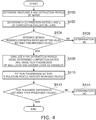
- FIG. 3 is a conduction band energy level diagram in the vertical direction of the active layer.
- the vertical axis is the relative conduction band energy (eV); and the horizontal axis is the vertical-direction position ( ⁇ m).
- One period of a multi-quantum well structure 80 included in the active layer 40 is made of a pair of a light-emitting multi-quantum well region 86 and an injection multi-quantum well region 88.
- the light-emitting multi-quantum well region 86 includes multiple well layers and multiple barrier layers.
- the well layer includes the second compound semiconductor.
- the barrier layer includes the first compound semiconductor.
- the composition evaluation layer 60 is provided on the front surface of the semiconductor laser wafer.
- the first film 61 is made of the first compound semiconductor included in the barrier layer.
- the second film 62 is made of the second compound semiconductor included in the well layer.
- the first compound semiconductor may be In x Al 1- x As (0 ⁇ x ⁇ 1); and the second compound semiconductor may be In y Ga 1- y As (0 ⁇ y ⁇ 0).
- the first film 61 may be the material included in the well layer; and the second film 62 may be the material included in the barrier layer.
- Table 1 illustrates a configuration example of one period of the set active layer structure included in the active layer 40.
- One period includes the pair of the light-emitting multi-quantum well region 86 and the injection multi-quantum well region 88.
- the well layers include In 0.669 Ga 0.331 As which is the second compound semiconductor; and the barrier layers include In 0.362 Al 0.638 As which is the first compound semiconductor.
- the light-emitting multi-quantum well region 86 includes four well layers; and the injection multi-quantum well region 88 includes seven well layers.
- the active layer 40 for example, 30 to 300 periods or the like of the quantum well structure are stacked.
- the composition ratio and/or the film thickness fluctuates easily due to external disturbances (the source material flux, the degree of vacuum, the growth temperature, etc.). Therefore, characteristic-defect wafers increase if the ridge waveguide formation, the electrode formation, the formation processes of the end surface reflective films, etc., are performed without performing an evaluation sort of the wafer after the crystal growth. Therefore, the overall yield of the semiconductor laser chips decreases. In other words, the chip yield decreases due to the fluctuation of the epitaxial crystal growth process.
- FIG. 4 is a flowchart of an evaluation process of the semiconductor laser wafer according to the first embodiment.
- X-rays (having a known wavelength ⁇ ) are irradiated on the front surface of the composition evaluation layer 60 provided on the semiconductor laser wafer 10; and the X-ray diffraction profile is determined by measuring the diffracted light intensity for the diffraction angles (S100).
- the composition ratios x and y are determined by utilizing the correlation between the lattice constant of the ternary compound mixed crystal and the composition ratio x (or y).
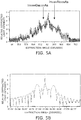
- FIG. 5A is a graph of the measured X-ray diffraction profile of the first embodiment
- FIG. 5B is a graph determined by simulating the X-ray diffraction profile of a sample structure in which a composition evaluation layer is formed on an InP substrate.
- the vertical axis is the relative diffracted light intensity; and the horizontal axis is the diffraction angle 2 ⁇ ( ⁇ : Bragg angle).
- the peak at the diffraction angle of about 63.3 degrees is InP which is the substrate 20.
- a subpeak of In y Ga 1- y As (0 ⁇ y ⁇ 1) occurs at the vicinity of 61.8 degrees at the left side of the peak of the substrate 20.
- a subpeak of In x Al 1- x As (0 ⁇ x ⁇ 1) occurs at the vicinity of 64.8 degrees at the right side of the peak of the substrate.
- the sample structure of FIG. 5B is a structure in which an In 0.362 Al 0.638 As film (set thickness: 20 nm) and an In 0.669 Ga 0.331 As film (set thickness: 20 nm) are provided in this order on an InP substrate.
- a subpeak of In 0.669 Ga 0.331 As occurs at a diffraction angle of about 61.8 degrees; and a subpeak of In 0.362 Al 0.638 As occurs at a diffraction angle of about 64.8 degrees.
- composition ratios x and y can be determined so that the X-ray diffraction profile that is obtained according to the simulation matches the measured X-ray diffraction profile of FIG. 5A (S102).
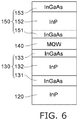
- FIG. 6 is a schematic cross-sectional view of a semiconductor laser wafer according to a comparative example.
- An active layer 140 has the same structure as that of Table 1; but a composition evaluation layer is not provided.
- the peak of the diffracted light intensity of In x Al 1- x As and the peak of the diffracted light intensity of In y Ga 1- y As of the composition evaluation layer are weak. Therefore, the accuracy of the composition ratios is insufficient when determining the composition ratios x and y from the measurement of the measured X-ray diffraction profile.
- the film thicknesses of the first film 61 and the second film 62 are less than 5 nm, the diffracted light intensity decreases; and the detection sensitivity decreases.
- the film thicknesses are greater than 30 nm, the crystallinity of the entire wafer decreases because the critical film thickness is approached. Therefore, it is favorable for the film thicknesses of the first film 61 and the second film 62 to be not less than 5 nm and not more than 30 nm.
- the composition ratios x and y are taken to be in the tolerance ranges (S104); and the flow proceeds to the next evaluation process.
- the wafer is determined to be a defective wafer because the composition ratios x and y do not satisfy the tolerance ranges (S106).
- the reference prescribed value can be set so that the absolute value of the difference between the determined composition ratio and the setting value (Table 1) is 10% of the setting value, etc.
- the chip yield can be increased by performing the evaluation process of the composition ratios x and y described above after the crystal growth process. To further increase the chip yield, it is favorable to add an evaluation process of the film thickness.
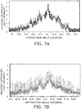
- FIG. 7A is a graph of the measured X-ray diffraction profile of the first embodiment
- FIG. 7B is a graph of an X-ray diffraction profile of the structure of the first embodiment determined by a simulation.
- FIG. 7A is the measured X-ray diffraction profile of the first embodiment and is the profile obtained in step S100 (the same as FIG. 5A ).
- the X-ray diffraction profile is simulated by setting the composition ratios of In to the composition ratios x and y determined in step S102 and by using the film thickness of the well layer and the film thickness of the barrier layer as variables (S108).
- film thicknesses corresponding to the last two layers (the InAIAs layer having a thickness of 2.7 nm and the InGaAs layer having a film thickness of 1.8 nm) of the MQW setting values of Table 1 can be used as the two variables.
- the assumptions of the simulation are that the growth rates of InGaAs and InAIAs are constant over the entire active layer 40, and the composition ratios x and y are the values determined in step S102.
- the two film thicknesses are fit so that the profile obtained by the simulation matches the measured X-ray profile ( FIG. 7A ) (S110).
- the correlation between the satellite peak and subpeak intensities, the diffraction angles, the film thicknesses, etc. can be utilized.
- the positions of the two film thicknesses used as variables can be selected from the configuration of Table 1.
- the film thicknesses (two) of the X-ray diffraction profile obtained by the fitting are determined to be in tolerance ranges when the differences between the film thicknesses (two) and the film thicknesses of the setting values of Table 1 are not more than the prescribed values (S112); and the wafer is determined to be a non-defective wafer. On the other hand, the wafer is determined to be a defective wafer when the film thickness differences are greater than the prescribed values (S114).
- the prescribed value can be set so that, for example, the absolute value of the film thickness difference is 10% of the setting value, etc.
- the composition evaluation layer 60 is provided between the active layer 40 and the wafer front surface or between the active layer 40 and the wafer front surface.
- the In composition ratio y of the well layer and the In composition ratio x of the barrier layer included in the active layer 40 are determined by the X-ray diffraction measurement in the wafer state.
- the X-ray diffraction profile is simulated by using the composition ratios x and y determined by the measurements and by using the film thickness of the well layer and the film thickness of the barrier layer as variables.
- the external disturbances that occur in the crystal growth process include not only the fluctuation of the source material flux but also the fluctuation of the degree of vacuum, the fluctuation of the growth temperature, etc. Therefore, the simulation accuracy of the film thickness fluctuation can be increased by performing the X-ray diffraction profile simulation of the wafer by using the four variables. As a result, the semiconductor laser chip yield can be increased.
- the diffraction angle where the diffracted light intensity is the peak is proximal to the InP diffraction angle for the cladding layers (e.g., InP) 32 and 52, the light guide layers (e.g., InGaAs) 33 and 51, the contact layers (e.g., InGaAs) 31 and 53, etc. Therefore, the effects on the X-ray diffraction profile can be small.
- the composition ratios of these layers can be determined individually.
- FIG. 8 is a schematic cross-sectional view of a semiconductor laser wafer according to a modification of the first embodiment.
- the composition evaluation layer 60 may be provided between the active layer 40 and the front surface of the semiconductor laser wafer 10. If the composition evaluation layer 60 is provided lower than the active layer 40, the optical path of the X-rays lengthens; attenuation and the like occurs; and the detection sensitivity decreases. In the modification of the first embodiment, a guide layer, a cladding layer, a contact layer, etc., are provided between the active layer 40 and the composition evaluation layer 60.
- the thickness of the cladding layer is large, i.e., 2 to 10 ⁇ m, etc.
- the impurity concentration of the contact layer is higher than the impurity concentration of the cladding layer. Therefore, there is a possibility that the growth conditions may be changed between the crystal growth process of the active layer 40 and the crystal growth process of the composition evaluation layer 60. Conversely, in the modification, the change of the growth conditions can be small between the crystal growth process of the active layer 40 and the crystal growth process of the composition evaluation layer 60. Therefore, the simulation accuracy can be high.
- the semiconductor laser may be an interband cascade laser (ICL).
- the active layer is provided on the first semiconductor layer and includes multiple periods of the pair of the light-emitting multi-quantum well region made of the first compound semiconductor and the second compound semiconductor and the injection multi-quantum well region made of the first compound semiconductor and the second compound semiconductor. Electrons are injected into the light-emitting multi-quantum well region from the electron injection layer of the injection multi-quantum well region on the upstream side; and holes are injected into the light-emitting multi-quantum well region from the injection multi-quantum well region on the downstream side.
- ICL interband cascade laser
- the electrons and the holes recombine in the light-emitting multi-quantum well region; and infrared laser light that corresponds to the interband transition level formed in the light-emitting multi-quantum well region is emitted.
- a semiconductor laser is provided in which the productivity of the semiconductor laser chip is high and infrared can be emitted.
- the semiconductor laser is utilized in environmental measurements, infrared detection, the detection of designated substances, etc.
Landscapes
- Physics & Mathematics (AREA)
- Condensed Matter Physics & Semiconductors (AREA)
- General Physics & Mathematics (AREA)
- Electromagnetism (AREA)
- Optics & Photonics (AREA)
- Geometry (AREA)
- Semiconductor Lasers (AREA)
- Analysing Materials By The Use Of Radiation (AREA)
- Testing Or Measuring Of Semiconductors Or The Like (AREA)
Applications Claiming Priority (1)
| Application Number | Priority Date | Filing Date | Title |
|---|---|---|---|
| JP2019034322A JP7129359B2 (ja) | 2019-02-27 | 2019-02-27 | 半導体レーザ用ウェーハおよび半導体レーザ |
Publications (3)
| Publication Number | Publication Date |
|---|---|
| EP3703200A2 true EP3703200A2 (fr) | 2020-09-02 |
| EP3703200A3 EP3703200A3 (fr) | 2020-12-23 |
| EP3703200B1 EP3703200B1 (fr) | 2025-05-07 |
Family
ID=69723795
Family Applications (1)
| Application Number | Title | Priority Date | Filing Date |
|---|---|---|---|
| EP20158198.0A Active EP3703200B1 (fr) | 2019-02-27 | 2020-02-19 | Wafer à laser semi-conducteur et laser semi-conducteur |
Country Status (3)
| Country | Link |
|---|---|
| US (1) | US11114821B2 (fr) |
| EP (1) | EP3703200B1 (fr) |
| JP (1) | JP7129359B2 (fr) |
Families Citing this family (2)
| Publication number | Priority date | Publication date | Assignee | Title |
|---|---|---|---|---|
| JP7411483B2 (ja) * | 2020-04-02 | 2024-01-11 | 浜松ホトニクス株式会社 | 量子カスケードレーザ素子の製造方法 |
| JP7662353B2 (ja) * | 2021-02-22 | 2025-04-15 | 株式会社東芝 | 面発光型半導体発光装置 |
Family Cites Families (11)
| Publication number | Priority date | Publication date | Assignee | Title |
|---|---|---|---|---|
| JPS6484684A (en) * | 1987-09-28 | 1989-03-29 | Toshiba Corp | Semiconductor laser and the preparation thereof |
| JPH09148667A (ja) * | 1995-11-22 | 1997-06-06 | Sanyo Electric Co Ltd | 半導体レーザ |
| JP3834748B2 (ja) | 2001-10-16 | 2006-10-18 | 日鉱金属株式会社 | 半導体単結晶の構造解析方法 |
| JP5641667B2 (ja) | 2007-01-18 | 2014-12-17 | 浜松ホトニクス株式会社 | 量子カスケードレーザ |
| JP5077303B2 (ja) * | 2008-10-07 | 2012-11-21 | 住友電気工業株式会社 | 窒化ガリウム系半導体発光素子、窒化ガリウム系半導体発光素子を作製する方法、窒化ガリウム系発光ダイオード、エピタキシャルウエハ、及び窒化ガリウム系発光ダイオードを作製する方法 |
| US8879595B2 (en) * | 2011-10-28 | 2014-11-04 | Wisconsin Alumni Research Foundation | Quantum cascade structures on metamorphic buffer layer structures |
| JP6161160B2 (ja) * | 2013-10-31 | 2017-07-12 | 国立研究開発法人理化学研究所 | 量子カスケードレーザー素子 |
| JP6259325B2 (ja) | 2014-03-12 | 2018-01-10 | 浜松ホトニクス株式会社 | 量子カスケードレーザ |
| EP3118949A4 (fr) * | 2014-03-13 | 2017-11-29 | Kabushiki Kaisha Toshiba | Dispositif laser à semiconducteur |
| JP6182230B1 (ja) * | 2016-03-15 | 2017-08-16 | 株式会社東芝 | 面発光量子カスケードレーザ |
| JP6557649B2 (ja) * | 2016-12-01 | 2019-08-07 | 株式会社東芝 | 量子カスケードレーザ |
-
2019
- 2019-02-27 JP JP2019034322A patent/JP7129359B2/ja active Active
- 2019-12-05 US US16/704,157 patent/US11114821B2/en active Active
-
2020
- 2020-02-19 EP EP20158198.0A patent/EP3703200B1/fr active Active
Also Published As
| Publication number | Publication date |
|---|---|
| US11114821B2 (en) | 2021-09-07 |
| EP3703200A3 (fr) | 2020-12-23 |
| JP2020141014A (ja) | 2020-09-03 |
| US20200274331A1 (en) | 2020-08-27 |
| JP7129359B2 (ja) | 2022-09-01 |
| EP3703200B1 (fr) | 2025-05-07 |
Similar Documents
| Publication | Publication Date | Title |
|---|---|---|
| JP5260909B2 (ja) | 受光デバイス | |
| US11201261B2 (en) | Deep ultraviolet light emitting element and method of manufacturing the same | |
| JPH033268A (ja) | 赤外線撮像装置及びその製造方法 | |
| US8817835B2 (en) | Quantum cascade laser | |
| Arimoto et al. | 150 mW fundamental-transverse-mode operation of 670 nm window laser diode | |
| EP3703200B1 (fr) | Wafer à laser semi-conducteur et laser semi-conducteur | |
| US7589347B2 (en) | Method for fabricating lateral semiconductor device | |
| US12117633B2 (en) | Optical filter | |
| US20020096675A1 (en) | Intersubband optical devices that operate at wavelengths shorter than 1.7 um | |
| US9960572B2 (en) | Semiconductor device | |
| DE112021002511B4 (de) | Halbleiterlaser und lidar-system mit dem halbleiterlaser | |
| US20030123501A1 (en) | Vertical cavity surface emitting laser including indium and antimony in the active region | |
| US7058112B2 (en) | Indium free vertical cavity surface emitting laser | |
| Ploog et al. | Preparation and properties of a new GaAs sawtooth doping superlattice | |
| US20030118069A1 (en) | Vertical cavity surface emitting laser including indium in the active region | |
| KR101606948B1 (ko) | 반도체 소자 및 반도체 소자의 제조 방법 | |
| Johnstone et al. | Electrical and optical characterization of GaSb based diode laser material for 2-4 μm applications | |
| DE2947805A1 (de) | Photodiode | |
| US4722087A (en) | Lead-strontium-chalcogenide diode laser | |
| US20030118068A1 (en) | Vertical cavity surface emitting laser including indium and nitrogen in the active region | |
| Kosiel et al. | High power (> 1 W) room-temperature (300 K) 980 nm continuous-wave AlGaAs/InGaAs/GaAs semiconductor lasers | |
| US20090141763A1 (en) | Semiconductor laser | |
| Greene et al. | Electroabsorptive In1-xGaxAsyP1-y superlattices grown by liquid phase epitaxy | |
| JP2825957B2 (ja) | 半導体受光素子 | |
| KR20020033413A (ko) | 3-5족 화합물 반도체 및 발광 소자 |
Legal Events
| Date | Code | Title | Description |
|---|---|---|---|
| PUAI | Public reference made under article 153(3) epc to a published international application that has entered the european phase |
Free format text: ORIGINAL CODE: 0009012 |
|
| STAA | Information on the status of an ep patent application or granted ep patent |
Free format text: STATUS: REQUEST FOR EXAMINATION WAS MADE |
|
| 17P | Request for examination filed |
Effective date: 20200219 |
|
| AK | Designated contracting states |
Kind code of ref document: A2 Designated state(s): AL AT BE BG CH CY CZ DE DK EE ES FI FR GB GR HR HU IE IS IT LI LT LU LV MC MK MT NL NO PL PT RO RS SE SI SK SM TR |
|
| AX | Request for extension of the european patent |
Extension state: BA ME |
|
| PUAL | Search report despatched |
Free format text: ORIGINAL CODE: 0009013 |
|
| AK | Designated contracting states |
Kind code of ref document: A3 Designated state(s): AL AT BE BG CH CY CZ DE DK EE ES FI FR GB GR HR HU IE IS IT LI LT LU LV MC MK MT NL NO PL PT RO RS SE SI SK SM TR |
|
| AX | Request for extension of the european patent |
Extension state: BA ME |
|
| RIC1 | Information provided on ipc code assigned before grant |
Ipc: H01S 5/00 20060101AFI20201116BHEP |
|
| STAA | Information on the status of an ep patent application or granted ep patent |
Free format text: STATUS: EXAMINATION IS IN PROGRESS |
|
| 17Q | First examination report despatched |
Effective date: 20230510 |
|
| RIC1 | Information provided on ipc code assigned before grant |
Ipc: H01S 5/343 20060101ALI20240925BHEP Ipc: H01S 5/34 20060101ALI20240925BHEP Ipc: H01S 5/22 20060101ALI20240925BHEP Ipc: H01S 5/00 20060101AFI20240925BHEP |
|
| GRAP | Despatch of communication of intention to grant a patent |
Free format text: ORIGINAL CODE: EPIDOSNIGR1 |
|
| STAA | Information on the status of an ep patent application or granted ep patent |
Free format text: STATUS: GRANT OF PATENT IS INTENDED |
|
| INTG | Intention to grant announced |
Effective date: 20241203 |
|
| GRAS | Grant fee paid |
Free format text: ORIGINAL CODE: EPIDOSNIGR3 |
|
| GRAA | (expected) grant |
Free format text: ORIGINAL CODE: 0009210 |
|
| STAA | Information on the status of an ep patent application or granted ep patent |
Free format text: STATUS: THE PATENT HAS BEEN GRANTED |
|
| AK | Designated contracting states |
Kind code of ref document: B1 Designated state(s): AL AT BE BG CH CY CZ DE DK EE ES FI FR GB GR HR HU IE IS IT LI LT LU LV MC MK MT NL NO PL PT RO RS SE SI SK SM TR |
|
| REG | Reference to a national code |
Ref country code: GB Ref legal event code: FG4D |
|
| RIN1 | Information on inventor provided before grant (corrected) |
Inventor name: TAKASE, TOMOHIRO Inventor name: YAMAMOTO, YUICHIRO Inventor name: KAKUNO, TSUTOMU Inventor name: HASHIMOTO, REI Inventor name: SAITO, SHINJI Inventor name: KANEKO, KEI |
|
| REG | Reference to a national code |
Ref country code: CH Ref legal event code: EP |
|
| REG | Reference to a national code |
Ref country code: DE Ref legal event code: R096 Ref document number: 602020050695 Country of ref document: DE |
|
| REG | Reference to a national code |
Ref country code: IE Ref legal event code: FG4D |
|
| REG | Reference to a national code |
Ref country code: NL Ref legal event code: MP Effective date: 20250507 |
|
| PG25 | Lapsed in a contracting state [announced via postgrant information from national office to epo] |
Ref country code: PT Free format text: LAPSE BECAUSE OF FAILURE TO SUBMIT A TRANSLATION OF THE DESCRIPTION OR TO PAY THE FEE WITHIN THE PRESCRIBED TIME-LIMIT Effective date: 20250908 Ref country code: FI Free format text: LAPSE BECAUSE OF FAILURE TO SUBMIT A TRANSLATION OF THE DESCRIPTION OR TO PAY THE FEE WITHIN THE PRESCRIBED TIME-LIMIT Effective date: 20250507 Ref country code: ES Free format text: LAPSE BECAUSE OF FAILURE TO SUBMIT A TRANSLATION OF THE DESCRIPTION OR TO PAY THE FEE WITHIN THE PRESCRIBED TIME-LIMIT Effective date: 20250507 |
|
| REG | Reference to a national code |
Ref country code: LT Ref legal event code: MG9D |
|
| PG25 | Lapsed in a contracting state [announced via postgrant information from national office to epo] |
Ref country code: NO Free format text: LAPSE BECAUSE OF FAILURE TO SUBMIT A TRANSLATION OF THE DESCRIPTION OR TO PAY THE FEE WITHIN THE PRESCRIBED TIME-LIMIT Effective date: 20250807 Ref country code: GR Free format text: LAPSE BECAUSE OF FAILURE TO SUBMIT A TRANSLATION OF THE DESCRIPTION OR TO PAY THE FEE WITHIN THE PRESCRIBED TIME-LIMIT Effective date: 20250808 |
|
| PG25 | Lapsed in a contracting state [announced via postgrant information from national office to epo] |
Ref country code: NL Free format text: LAPSE BECAUSE OF FAILURE TO SUBMIT A TRANSLATION OF THE DESCRIPTION OR TO PAY THE FEE WITHIN THE PRESCRIBED TIME-LIMIT Effective date: 20250507 Ref country code: PL Free format text: LAPSE BECAUSE OF FAILURE TO SUBMIT A TRANSLATION OF THE DESCRIPTION OR TO PAY THE FEE WITHIN THE PRESCRIBED TIME-LIMIT Effective date: 20250507 |
|
| REG | Reference to a national code |
Ref country code: AT Ref legal event code: MK05 Ref document number: 1793573 Country of ref document: AT Kind code of ref document: T Effective date: 20250507 |
|
| PG25 | Lapsed in a contracting state [announced via postgrant information from national office to epo] |
Ref country code: BG Free format text: LAPSE BECAUSE OF FAILURE TO SUBMIT A TRANSLATION OF THE DESCRIPTION OR TO PAY THE FEE WITHIN THE PRESCRIBED TIME-LIMIT Effective date: 20250507 |
|
| PG25 | Lapsed in a contracting state [announced via postgrant information from national office to epo] |
Ref country code: HR Free format text: LAPSE BECAUSE OF FAILURE TO SUBMIT A TRANSLATION OF THE DESCRIPTION OR TO PAY THE FEE WITHIN THE PRESCRIBED TIME-LIMIT Effective date: 20250507 |
|
| PG25 | Lapsed in a contracting state [announced via postgrant information from national office to epo] |
Ref country code: AT Free format text: LAPSE BECAUSE OF FAILURE TO SUBMIT A TRANSLATION OF THE DESCRIPTION OR TO PAY THE FEE WITHIN THE PRESCRIBED TIME-LIMIT Effective date: 20250507 |
|
| PG25 | Lapsed in a contracting state [announced via postgrant information from national office to epo] |
Ref country code: RS Free format text: LAPSE BECAUSE OF FAILURE TO SUBMIT A TRANSLATION OF THE DESCRIPTION OR TO PAY THE FEE WITHIN THE PRESCRIBED TIME-LIMIT Effective date: 20250807 |
|
| PG25 | Lapsed in a contracting state [announced via postgrant information from national office to epo] |
Ref country code: IS Free format text: LAPSE BECAUSE OF FAILURE TO SUBMIT A TRANSLATION OF THE DESCRIPTION OR TO PAY THE FEE WITHIN THE PRESCRIBED TIME-LIMIT Effective date: 20250907 |
|
| PG25 | Lapsed in a contracting state [announced via postgrant information from national office to epo] |
Ref country code: LV Free format text: LAPSE BECAUSE OF FAILURE TO SUBMIT A TRANSLATION OF THE DESCRIPTION OR TO PAY THE FEE WITHIN THE PRESCRIBED TIME-LIMIT Effective date: 20250507 |
|
| PG25 | Lapsed in a contracting state [announced via postgrant information from national office to epo] |
Ref country code: SM Free format text: LAPSE BECAUSE OF FAILURE TO SUBMIT A TRANSLATION OF THE DESCRIPTION OR TO PAY THE FEE WITHIN THE PRESCRIBED TIME-LIMIT Effective date: 20250507 Ref country code: DK Free format text: LAPSE BECAUSE OF FAILURE TO SUBMIT A TRANSLATION OF THE DESCRIPTION OR TO PAY THE FEE WITHIN THE PRESCRIBED TIME-LIMIT Effective date: 20250507 |
|
| PG25 | Lapsed in a contracting state [announced via postgrant information from national office to epo] |
Ref country code: CZ Free format text: LAPSE BECAUSE OF FAILURE TO SUBMIT A TRANSLATION OF THE DESCRIPTION OR TO PAY THE FEE WITHIN THE PRESCRIBED TIME-LIMIT Effective date: 20250507 |
|
| PG25 | Lapsed in a contracting state [announced via postgrant information from national office to epo] |
Ref country code: EE Free format text: LAPSE BECAUSE OF FAILURE TO SUBMIT A TRANSLATION OF THE DESCRIPTION OR TO PAY THE FEE WITHIN THE PRESCRIBED TIME-LIMIT Effective date: 20250507 |
|
| PG25 | Lapsed in a contracting state [announced via postgrant information from national office to epo] |
Ref country code: SK Free format text: LAPSE BECAUSE OF FAILURE TO SUBMIT A TRANSLATION OF THE DESCRIPTION OR TO PAY THE FEE WITHIN THE PRESCRIBED TIME-LIMIT Effective date: 20250507 Ref country code: RO Free format text: LAPSE BECAUSE OF FAILURE TO SUBMIT A TRANSLATION OF THE DESCRIPTION OR TO PAY THE FEE WITHIN THE PRESCRIBED TIME-LIMIT Effective date: 20250507 |
|
| PG25 | Lapsed in a contracting state [announced via postgrant information from national office to epo] |
Ref country code: IT Free format text: LAPSE BECAUSE OF FAILURE TO SUBMIT A TRANSLATION OF THE DESCRIPTION OR TO PAY THE FEE WITHIN THE PRESCRIBED TIME-LIMIT Effective date: 20250507 |
|
| REG | Reference to a national code |
Ref country code: DE Ref legal event code: R097 Ref document number: 602020050695 Country of ref document: DE |
|
| PLBE | No opposition filed within time limit |
Free format text: ORIGINAL CODE: 0009261 |
|
| STAA | Information on the status of an ep patent application or granted ep patent |
Free format text: STATUS: NO OPPOSITION FILED WITHIN TIME LIMIT |
|
| REG | Reference to a national code |
Ref country code: CH Ref legal event code: L10 Free format text: ST27 STATUS EVENT CODE: U-0-0-L10-L00 (AS PROVIDED BY THE NATIONAL OFFICE) Effective date: 20260318 |
|
| PGFP | Annual fee paid to national office [announced via postgrant information from national office to epo] |
Ref country code: DE Payment date: 20251224 Year of fee payment: 7 |
|
| 26N | No opposition filed |
Effective date: 20260210 |