EP3707774B1 - Millimeterwellenübertragungsleitungsarchitektur - Google Patents
Millimeterwellenübertragungsleitungsarchitektur Download PDFInfo
- Publication number
- EP3707774B1 EP3707774B1 EP18812464.8A EP18812464A EP3707774B1 EP 3707774 B1 EP3707774 B1 EP 3707774B1 EP 18812464 A EP18812464 A EP 18812464A EP 3707774 B1 EP3707774 B1 EP 3707774B1
- Authority
- EP
- European Patent Office
- Prior art keywords
- transmission line
- dielectric substrate
- ground plane
- pair
- reference conductors
- Prior art date
- Legal status (The legal status is an assumption and is not a legal conclusion. Google has not performed a legal analysis and makes no representation as to the accuracy of the status listed.)
- Active
Links
Images


Classifications
-
- H—ELECTRICITY
- H01—ELECTRIC ELEMENTS
- H01P—WAVEGUIDES; RESONATORS, LINES, OR OTHER DEVICES OF THE WAVEGUIDE TYPE
- H01P3/00—Waveguides; Transmission lines of the waveguide type
- H01P3/003—Coplanar lines
- H01P3/006—Conductor backed coplanar waveguides
-
- H—ELECTRICITY
- H01—ELECTRIC ELEMENTS
- H01P—WAVEGUIDES; RESONATORS, LINES, OR OTHER DEVICES OF THE WAVEGUIDE TYPE
- H01P11/00—Apparatus or processes specially adapted for manufacturing waveguides or resonators, lines, or other devices of the waveguide type
- H01P11/001—Manufacturing waveguides or transmission lines of the waveguide type
- H01P11/003—Manufacturing lines with conductors on a substrate, e.g. strip lines, slot lines
-
- H—ELECTRICITY
- H01—ELECTRIC ELEMENTS
- H01P—WAVEGUIDES; RESONATORS, LINES, OR OTHER DEVICES OF THE WAVEGUIDE TYPE
- H01P3/00—Waveguides; Transmission lines of the waveguide type
- H01P3/02—Waveguides; Transmission lines of the waveguide type with two longitudinal conductors
- H01P3/08—Microstrips; Strip lines
- H01P3/081—Microstriplines
- H01P3/082—Multilayer dielectric
-
- H—ELECTRICITY
- H01—ELECTRIC ELEMENTS
- H01P—WAVEGUIDES; RESONATORS, LINES, OR OTHER DEVICES OF THE WAVEGUIDE TYPE
- H01P3/00—Waveguides; Transmission lines of the waveguide type
- H01P3/02—Waveguides; Transmission lines of the waveguide type with two longitudinal conductors
- H01P3/08—Microstrips; Strip lines
- H01P3/085—Triplate lines
-
- H—ELECTRICITY
- H05—ELECTRIC TECHNIQUES NOT OTHERWISE PROVIDED FOR
- H05K—PRINTED CIRCUITS; CASINGS OR CONSTRUCTIONAL DETAILS OF ELECTRIC APPARATUS; MANUFACTURE OF ASSEMBLAGES OF ELECTRICAL COMPONENTS
- H05K1/00—Printed circuits
- H05K1/02—Details
- H05K1/0213—Electrical arrangements not otherwise provided for
- H05K1/0216—Reduction of cross-talk, noise or electromagnetic interference
- H05K1/0218—Reduction of cross-talk, noise or electromagnetic interference by printed shielding conductors, ground planes or power plane
- H05K1/0219—Printed shielding conductors for shielding around or between signal conductors, e.g. coplanar or coaxial printed shielding conductors
-
- H—ELECTRICITY
- H05—ELECTRIC TECHNIQUES NOT OTHERWISE PROVIDED FOR
- H05K—PRINTED CIRCUITS; CASINGS OR CONSTRUCTIONAL DETAILS OF ELECTRIC APPARATUS; MANUFACTURE OF ASSEMBLAGES OF ELECTRICAL COMPONENTS
- H05K1/00—Printed circuits
- H05K1/02—Details
- H05K1/0213—Electrical arrangements not otherwise provided for
- H05K1/0216—Reduction of cross-talk, noise or electromagnetic interference
- H05K1/0218—Reduction of cross-talk, noise or electromagnetic interference by printed shielding conductors, ground planes or power plane
- H05K1/0224—Patterned shielding planes, ground planes or power planes
-
- H—ELECTRICITY
- H05—ELECTRIC TECHNIQUES NOT OTHERWISE PROVIDED FOR
- H05K—PRINTED CIRCUITS; CASINGS OR CONSTRUCTIONAL DETAILS OF ELECTRIC APPARATUS; MANUFACTURE OF ASSEMBLAGES OF ELECTRICAL COMPONENTS
- H05K1/00—Printed circuits
- H05K1/02—Details
- H05K1/11—Printed elements for providing electric connections to or between printed circuits
- H05K1/115—Via connections; Lands around holes or via connections
-
- H—ELECTRICITY
- H05—ELECTRIC TECHNIQUES NOT OTHERWISE PROVIDED FOR
- H05K—PRINTED CIRCUITS; CASINGS OR CONSTRUCTIONAL DETAILS OF ELECTRIC APPARATUS; MANUFACTURE OF ASSEMBLAGES OF ELECTRICAL COMPONENTS
- H05K3/00—Apparatus or processes for manufacturing printed circuits
- H05K3/0011—Working of insulating substrates or insulating layers
- H05K3/0044—Mechanical working of the substrate, e.g. drilling or punching
-
- H—ELECTRICITY
- H05—ELECTRIC TECHNIQUES NOT OTHERWISE PROVIDED FOR
- H05K—PRINTED CIRCUITS; CASINGS OR CONSTRUCTIONAL DETAILS OF ELECTRIC APPARATUS; MANUFACTURE OF ASSEMBLAGES OF ELECTRICAL COMPONENTS
- H05K3/00—Apparatus or processes for manufacturing printed circuits
- H05K3/02—Apparatus or processes for manufacturing printed circuits in which the conductive material is applied to the surface of the insulating support and is thereafter removed from such areas of the surface which are not intended for current conducting or shielding
- H05K3/04—Apparatus or processes for manufacturing printed circuits in which the conductive material is applied to the surface of the insulating support and is thereafter removed from such areas of the surface which are not intended for current conducting or shielding the conductive material being removed mechanically, e.g. by punching
-
- H—ELECTRICITY
- H05—ELECTRIC TECHNIQUES NOT OTHERWISE PROVIDED FOR
- H05K—PRINTED CIRCUITS; CASINGS OR CONSTRUCTIONAL DETAILS OF ELECTRIC APPARATUS; MANUFACTURE OF ASSEMBLAGES OF ELECTRICAL COMPONENTS
- H05K3/00—Apparatus or processes for manufacturing printed circuits
- H05K3/10—Apparatus or processes for manufacturing printed circuits in which conductive material is applied to the insulating support in such a manner as to form the desired conductive pattern
- H05K3/107—Apparatus or processes for manufacturing printed circuits in which conductive material is applied to the insulating support in such a manner as to form the desired conductive pattern by filling grooves in the support with conductive material
-
- H—ELECTRICITY
- H05—ELECTRIC TECHNIQUES NOT OTHERWISE PROVIDED FOR
- H05K—PRINTED CIRCUITS; CASINGS OR CONSTRUCTIONAL DETAILS OF ELECTRIC APPARATUS; MANUFACTURE OF ASSEMBLAGES OF ELECTRICAL COMPONENTS
- H05K3/00—Apparatus or processes for manufacturing printed circuits
- H05K3/22—Secondary treatment of printed circuits
- H05K3/28—Applying non-metallic protective coatings
-
- H—ELECTRICITY
- H05—ELECTRIC TECHNIQUES NOT OTHERWISE PROVIDED FOR
- H05K—PRINTED CIRCUITS; CASINGS OR CONSTRUCTIONAL DETAILS OF ELECTRIC APPARATUS; MANUFACTURE OF ASSEMBLAGES OF ELECTRICAL COMPONENTS
- H05K2201/00—Indexing scheme relating to printed circuits covered by H05K1/00
- H05K2201/09—Shape and layout
- H05K2201/09209—Shape and layout details of conductors
- H05K2201/0929—Conductive planes
- H05K2201/093—Layout of power planes, ground planes or power supply conductors, e.g. having special clearance holes therein
-
- H—ELECTRICITY
- H05—ELECTRIC TECHNIQUES NOT OTHERWISE PROVIDED FOR
- H05K—PRINTED CIRCUITS; CASINGS OR CONSTRUCTIONAL DETAILS OF ELECTRIC APPARATUS; MANUFACTURE OF ASSEMBLAGES OF ELECTRICAL COMPONENTS
- H05K2201/00—Indexing scheme relating to printed circuits covered by H05K1/00
- H05K2201/09—Shape and layout
- H05K2201/09818—Shape or layout details not covered by a single group of H05K2201/09009 - H05K2201/09809
- H05K2201/09854—Hole or via having special cross-section, e.g. elliptical
Definitions
- Radio frequency (RF) and electromagnetic circuits may be manufactured using conventional printed circuit board (PCB) processes.
- PCB manufacturing processes may include lamination, electroplating, masking, etching, and other complex process steps, and may require multiple steps, expensive and/or hazardous materials, multiple iterations, extensive labor, etc., all leading to higher cost and slower turnaround time. Additionally, conventional PCB manufacturing processes have limited ability to allow for small feature sizes, such as transmission line (e.g., stripline) dimensions, and dimensions of dielectric materials between conductors (e.g., dielectric thickness, inter-via spacing, etc.), thereby limiting the range of highest frequency signals that may be supported by such circuits.
- transmission line e.g., stripline
- dielectric materials between conductors e.g., dielectric thickness, inter-via spacing, etc.
- US Pub. No. 2010/0182105 A1 discloses a waveguide system for distributing high-bandwidth signals in a multilayer circuit carrier.
- the waveguide system comprises at least one coplanar waveguide and one or more ground wires.
- the coplanar waveguide is disposed with the ground wires associated therewith between at least two insulating layers of the circuit carrier.
- the surface of the two insulating layers oriented away from the plane of the waveguide has electrically conductive layers.
- Electrically conductive plated through-holes extend along the waveguide substantially perpendicular to the plane of the waveguide.
- the ground wires, the electrically conductive layers, and the plated through-holes are electrically connected to ground potential.
- the waveguide system serves particularly for the three-dimensional distribution of high-bandwidth signals.
- US Pub. No. 6,674,347 B1 discloses a multi-layer substrate comprising a first dielectric layer, a coplanar waveguide line formed on a first surface of the first dielectric layer, the coplanar waveguide line including a signal conductor and a pair of ground conductor layers positioned at opposite sides of the signal conductor, separately from the signal conductor, and a second dielectric layer formed to cover the coplanar waveguide line and the first dielectric layer and having an opening positioned at least on the signal conductor of the coplanar waveguide line.
- a thickness of the first dielectric layer is smaller than the value of c / ⁇ 4 f ( ⁇ 1 - 1) 1/2 ⁇ , where c is velocity of light, f is a frequency of a signal propagating in the signal line, and ⁇ 1 is a dielectric constant of the first dielectric layer.
- US Pub. No. 2010/0254094 A1 discloses a high-frequency wiring board that includes first coplanar lines and second coplanar lines formed on a different layer than the first coplanar lines; the first coplanar lines and second coplanar lines being connected at the line ends of each.
- the first coplanar lines are provided with a first signal line and a first planar ground pattern formed on the same wiring layer as the first signal line.
- the second coplanar lines are provided with second signal line formed on a wiring layer that differs from that of the first signal line, a second planar ground pattern formed on the same wiring layer as the second signal line, and a first ground pattern formed on the same wiring layer as the first coplanar lines.
- the second planar ground pattern is separated from the connection portion at the end of the first planar ground pattern in the direction in which the second coplanar lines extend from the vicinity of the connection portion of the first signal line and the second signal line.
- US Pub. No. 2015/0323576 A1 discloses an electrical cell that enables experimental measurements of dielectric properties of an electrochromic material in the radio-frequency range of the electromagnetic spectrum.
- the electrical cell includes a layer of the electrochromic material under test that is sandwiched between a conducting base plane and a microstrip line.
- the conducting base plane and the micro strip line are electrically connected to a coplanar waveguide configured for application of superimposed DC-bias and RF-probe signals using a conventional probe station and a vector network analyzer.
- the S-parameters of the electrical cell measured in this manner can then be used, e.g., to obtain the complex dielectric constant of the electrochromic material under test as a func-tion of frequency.
- US Pub. No. 5 828 555 A discloses a multilayer printed-circuit board that includes at least one inner-layer signal line, first and second ground layers between which the inner-layer signal line is sandwiched via a frame member made of an insulating material in a thickness direction of the multilayer printed-circuit board, and metallic wall members which are provided on inner walls of slits formed in the frame member and extending along the inner-layer signal line.
- the first and second ground layers and the metallic wall members shield the inner-layer signal line.
- M FARHAN SHAFIQUE ET AL "Laser machining of microvias and trenches for substrate integrated waveguides in LTCC technology", MICROWAVE CONFERENCE, 2009. EUMC 2009. EUROPEAN, 1 October 2009 (2009-10-01), pages 272-275 discloses that: the fabrication of microvias and trenches for substrate integrated waveguides (SIWs) in low temperature co-fired ceramic (LTCC) technology is studied using a commercial laser PCB prototyping system. It is shown that by careful control of the laser beam around the edge of the via, clean holes can be produced. Vias with diameter of 75 ⁇ m and trenches with width of 60 ⁇ m are demonstrated. The effects of laser parameters in making vias and trenches are investigated. The process can be utilized to demonstrate LTCC SIWs operating in the 25-40 GHz range with low loss. It is confirmed that rows of via-holes can achieve the same performance as solid sidewalls.
- a continuous conducting structure may be formed in one or more dielectric substrates by machining a trench and filling the trench with a conductor, such as a conductive ink applied using 3-D printing techniques, to form an electromagnetic boundary.
- a conductor such as a conductive ink applied using 3-D printing techniques
- Such an electromagnetic boundary may enforce boundary conditions of an electromagnetic signal, e.g., to control or limit modes of a signal and/or characteristic impedance, or may provide isolation to confine signals to a region of an electromagnetic circuit, e.g., a Faraday boundary to prevent a signal at one region of the circuit from affecting another region of the circuit, e.g., shielding.
- radio frequency as used herein is not intended to be limited to a particular frequency, range of frequencies, band, spectrum, etc., unless explicitly stated and/or specifically indicated by context.
- radio frequency signal and “electromagnetic signal” are used interchangeably and may refer to a signal of various suitable frequency for the propagation of information-carrying signals, for any particular implementation.
- Such radio frequency signals may generally be bound at the low end by frequencies in the kilohertz (kHz) range, and bound at the high end by frequencies of up to hundreds of gigahertz (GHz), and explicitly includes signals in the microwave or millimeter wave ranges.
- systems and methods in accord with those described herein may be suitable for handling non-ionizing radiation, at frequencies below those conventionally handled in the field of optics, e.g., of lower frequency than, e.g., infrared signals.
- the transmission line 120 is circumscribed by reference conductors 126, which are co-planar conductors, providing a secondary or "return path" electrical conductor for signals conveyed by the transmission line 120.
- the term "transmission line” may include the combination of the transmission line 120 (a first conductor) and its associated reference conductors 126 (a second conductor).
- the reference conductors 126 may be coupled to a ground reference.
- the transmission line 120 exhibits a characteristic impedance for signals of various frequencies, and the characteristic impedance may depend upon a size of the transmission line 120 (e.g., height and width), a size of the gap(s) between the transmission line 120 and the reference conductors 126, and material characteristics of the substrates 110 and the gap(s).
- gaps between the transmission line 120 and the reference conductors 126 may be filled with a bonding material, e.g., and adhesive used to bond the substrates 110 together.
- the transmission line 120 may also have an electrical connection, such as by solder, to a "vertical launch" conductor 130, which may be disposed within a machined hole in the substrate 110b. Accordingly, the conductor 130 and the transmission line 120 may form an electrically continuous signal conveyance, and each may convey and provide signals beyond the extent of the portion shown in FIG. 1 .
- the conductor 130 may be a segment of wire, such as a copper wire.
- the conductor 130 may be any of various forms, such as solid, hollow, rigid, flexible, straight, coil, spiral, etc. Additional details of at least one example of a vertical launch and its manufacture are disclosed in U.S. Patent Application No. 15/988,296 titled ADDITIVE MANUFACTURING TECHNOLOGY MICROWAVE VERTICAL LAUNCH filed on May 24, 2018 .
- a ground plane 140 may be provided and may be formed of a conductive cladding disposed upon a "bottom" surface of the substrate 110a.
- An additional ground plane 150 may be provided upon a "top" surface of the substrate 110b.
- the ground plane 150 may be formed by a conductive cladding disposed upon the substrate 110b.
- a portion of the conductive cladding may be removed by machining (e.g., milling) to provide a ground plane with an appropriate physical dimension, shape, or extent, e.g., to be suitable to act as the ground plane 150.
- a "top" of the Faraday wall 160 may be in electrical contact with the ground plane 150, which may be accomplished by slight over-filling of the machined trench to ensure contact between the conductive ink and the ground plane 150 and/or by application of solder, for example. Additional details of at least one example of a Faraday wall and its manufacture are disclosed in U.S. Provisional Patent Application No. 62/673,491 titled ADDITIVE MANUFACTURING TECHNOLOGY (AMT) FARADAY BOUNDARIES IN RADIO FREQUENCY CIRCUITS filed on May 18, 2018 .
- the ground plane 140, ground plane 150, and Faraday wall 160 together form a substantially electrically continuous conductor that provides an isolation boundary for signal(s) conveyed by the transmission line 120 and its associated reference conductors 126.
- dimensional placement of the ground planes 140, 150 and the Faraday wall 160 may be selected to control or limit a propagating mode of a signal conveyed by the transmission line 120 and/or to establish a characteristic impedance for signal(s) conveyed by the transmission line 120.
- the ground planes 140, 150 and the Faraday wall 160 may be positioned such that only a transverse electromagnetic (TEM) signal mode may propagate along the transmission line 120.
- the Faraday wall 160 may be positioned to isolate one portion of a circuit from another portion of a circuit without enforcing a particular propagating mode and/or without contributing to an impedance for any particular signal(s).
- TEM transverse electromagnetic
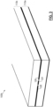
- the structure 100 is merely an example and portion of a structure in which an electromagnetic circuit may be provided. Further extent of the substrates shown may accommodate various circuit components, and additional substrates having additional layers to accommodate additional circuit components may be provided in various embodiments. Typically, a portion of a circuit may be disposed on a particular layer, and may include ground planes above and/or below, and other portions of a total circuit (or system) may exist at different regions of the same layer or on other layers.
- FIG. 2 shows a portion structure 100a of the circuit structure 100 at one stage of manufacture, in accord with aspects and embodiments of the systems and methods described herein.
- the portion structure 100a includes the substrate 110a which may be provided with conductive (e.g., copper) cladding on various surfaces.
- the substrate 110a has a conductive cladding 112 on one surface that serves as the conductive material from which the transmission line 120 and the reference conductors 126 are formed.
- the substrate 110a has a conductive cladding on an opposing surface to serve as the ground plane 140.
- the transmission line 120 may be formed by machining away at least a portion 122 of the cladding 112, thereby leaving a portion of conductive material to serve as the transmission line 120, distinct from the remainder of the cladding 112.
- FIG. 3 shows another portion structure 100b of the circuit structure 100 at another stage of manufacture.
- the substrate 110b is aligned with the substrate 110a, to be bonded together.
- a temporary bonding or affixing may be applied and a permanent bonding step may be applied at a later time, such as a bonding that may require heat or baking to cure or to secure a permanency of the bonding.
- Various examples may have a hole in the substrate 110b positioned to align with a portion of the transmission line 120, e.g., to accommodate the conductor 130 illustrated in FIG. 1 .
- a "top" surface of the substrate 110b may include a conductive cladding, which may be used to provide a ground plane, if desired. As with the cladding 112, portions of any cladding on the substrate 110b may be machined away to form various other structures, components, or a ground plane having a desired shape or extent.
- the conductive cladding 112 from which the transmission line 120 is formed may equivalently be associated with the substrate 110b, e.g., on a "bottom" side with respect to FIG. 3 , instead of being associated with the substrate 110a.
- the conductive material from which the transmission line 120 is provided may be a conductive cladding associated with either of the substrates 110.
- the transmission line 120 and/or the reference conductors 126 may be provided from differing materials and/or through other means in various embodiments.
- FIG. 4 shows another portion structure 100c of the circuit structure 100 at another stage of manufacture.
- a trench 162 is milled through the substrates 110.
- the trench 162 is milled through the substrates 110 and a portion of the cladding 112, down to the conductive cladding that forms the ground plane 140. Machining away material to form the trench 162 may also form the reference conductors 126, e.g., by separating a further portion of the cladding 112, leaving a portion of conductive material to serve as the reference conductors 126, distinct from the remainder of the cladding 112.
- the trench 162 is milled down to the ground plane 140 without piercing the ground plane 140.
- the intact ground plane 140 may provide structural support to portions of the structure 100c while the trench is empty.
- FIG. 5 shows another portion structure 100d of the circuit structure 100 at another stage of manufacture.
- the trench 162 is filled with a conductive fill 164 to form the Faraday wall 160.
- the conductive fill 164 may make electrical contact with the ground plane 140 to form a substantially electrically continuous ground boundary.
- a further ground plane 150 may be included, and to which the conductive fill 164 may be electrically connected by physical contact and/or by further application of solder at positions along the Faraday wall 160, to electrically join with the ground plane 150.
- electromagnetic circuits with an overall thickness of 10 mils (.010 inches, 254 microns) or less, and may include transmission lines, such as the traces as narrow as 4.4 mils (111.8 microns), 2.7 mils (68.6 microns), or even as narrow as 1.97 mils (50 microns), depending upon the tolerances and accuracy of various milling and additive manufacturing equipment used.
- electromagnetic circuits in accord with those described herein may be suitable for microwave and millimeter wave applications, including S-Band, X-Band, K-Bands, and higher frequencies, with various embodiments capable of accommodating frequencies over 28 GHz and up to 70 GHz or higher. Some embodiments may be suitable for frequency ranges up to 300 GHz or more.
- electromagnetic circuits manufactured in accord with methods described herein accommodate less expensive and faster prototyping, without the necessity for caustic chemicals, masking, etching, electroplating, etc.
- Simple substrates with pre-plated conductive material disposed on one or both surfaces (sides) may form the core starting material, and all elements of an electromagnetic circuit may be formed by milling (subtractive, drilling), filling (additive, printing of conductive and/or resistive inks), and bonding one or more substrates.
- Simple solder reflow operations and insertion of simple conductors are accommodated by methods and systems described herein.
- electromagnetic circuits manufactured in accord with methods described herein may accommodate deployment on, or designs calling for, non-planar surfaces.
- Thin, low-profile electromagnetic circuits, such as described herein and others, may be manufactured using mill, fill, and bond techniques as described herein to produce electromagnetic circuits having any desired contour, to adhere to a surface (such as a vehicle) or to support a complex array structure, for instance.
Landscapes
- Engineering & Computer Science (AREA)
- Microelectronics & Electronic Packaging (AREA)
- Manufacturing & Machinery (AREA)
- Physics & Mathematics (AREA)
- Electromagnetism (AREA)
- Structure Of Printed Boards (AREA)
- Production Of Multi-Layered Print Wiring Board (AREA)
- Waveguides (AREA)
Claims (11)
- Hochfrequenzschaltung (100), umfassend:ein erstes dielektrisches Substrat (110a) mit einer ersten Oberfläche;ein zweites dielektrisches Substrat (110b) mit einer zweiten Oberfläche, wobei das erste und das zweite dielektrische Substrat so relativ zueinander positioniert sind, dass die zweite Oberfläche der ersten Oberfläche zugewandt ist;eine Übertragungsleitung (120), die aus einer leitfähigen Ummantelung (112) gebildet ist, die auf der ersten Oberfläche angeordnet ist, wobei die Übertragungsleitung zumindest teilweise zwischen dem ersten dielektrischen Substrat und dem zweiten dielektrischen Substrat eingekapselt ist;ein Paar Referenzleiter (126), wobei jeder des Paars Referenzleiter benachbart und koplanar zu der Übertragungsleitung positioniert und so beabstandet ist, dass zwischen jedem des Paars Referenzleiter und der Übertragungsleitung ein Spalt besteht, wobei jeder des Paars Referenzleiter auf der ersten Oberfläche oder der zweiten Oberfläche angeordnet und zumindest teilweise zwischen dem ersten dielektrischen Substrat und dem zweiten dielektrischen Substrat eingekapselt ist;eine erste Masseebene (140), die auf einer dritten Oberfläche des ersten dielektrischen Substrats vorgesehen ist, wobei die dritte Oberfläche eine gegenüberliegende und im Wesentlichen parallele Oberfläche zur ersten Oberfläche ist, und eine zweite Masseebene (150), die auf einer vierten Oberfläche des zweiten dielektrischen Substrats vorgesehen ist, wobei die vierte Oberfläche eine gegenüberliegende und im Wesentlichen parallele Oberfläche zur zweiten Oberfläche ist, wobei jede der ersten Masseebene und der zweiten Masseebene im Wesentlichen parallel zueinander und zur koplanaren Anordnung der Übertragungsleitung und des Paars Referenzleiter ist; undeine Nut (162), die durch das erste dielektrische Substrat und das zweite dielektrische Substrat gebildet ist, wobei die Nut zwischen der ersten Masseebene und der zweiten Masseebene verläuft und im Wesentlichen senkrecht zu diesen ist, wobei die Nut die erste Masseebene nicht durchstößt, wobei ein leitfähiges Material (164) in die Nut gefüllt ist und wobei das leitfähige Material so angeordnet ist, dass es in elektrischem Kontakt mit der ersten Masseebene und der zweiten Masseebene steht.
- Die Hochfrequenzschaltung nach Anspruch 1, wobei das Paar Referenzleiter aus der auf dem ersten Substrat angeordneten leitfähigen Ummantelung gebildet ist.
- Die Hochfrequenzschaltung nach Anspruch 1, wobei das leitfähige Material in elektrischem Kontakt mit dem Paar Referenzleiter steht.
- Die Hochfrequenzschaltung nach Anspruch 1, die außerdem einen elektrischen Leiter umfasst, der durch ein Loch in mindestens einem der ersten dielektrischen Substrate und der zweiten dielektrischen Substrate verläuft, wobei der elektrische Leiter in elektrischem Kontakt mit der Übertragungsleitung steht.
- Die Hochfrequenzschaltung nach Anspruch 4, die außerdem eine elektrische Komponente in elektrischem Kontakt mit dem elektrischen Leiter umfasst und dazu konfiguriert ist, ein elektromagnetisches Signal über den elektrischen Leiter an die Übertragungsleitung zu senden oder von dieser zu empfangen, wobei die elektrische Komponente mindestens eines der folgenden Elemente ist: eine Anschlussklemme, ein Verbinder, ein Kabel und ein elektromagnetischer Strahler.
- Die Hochfrequenzschaltung nach Anspruch 1, wobei die Übertragungsleitung bei 70 GHz einen Einfügungsverlust von 1,2 Dezibel oder weniger pro Zoll erzeugt.
- Verfahren zur Herstellung eines elektromagnetischen Schaltkreises, wobei das Verfahren umfasst:Bereitstellen eines ersten dielektrischen Substrats mit einer auf einer ersten Oberfläche davon angeordneten leitfähigen Ummantelung;Bearbeiten der leitenden Ummantelung, um einen Teil der leitenden Ummantelung zu entfernen und so eine Übertragungsleitung zu bilden, wobei der entfernte Teil einen jeweiligen Spalt zwischen der Übertragungsleitung und einem verbleibenden Teil der leitenden Ummantelung bildet und zumindest ein Teil des verbleibenden Teils der leitenden Ummantelung ein Paar Referenzleiter auf beiden Seiten der Übertragungsleitung und in einer Ebene mit dieser bildet;Bereitstellen eines zweiten dielektrischen Substrats mit einer zweiten Oberfläche und Positionieren des zweiten dielektrischen Substrats so, dass die zweite Oberfläche der ersten Oberfläche zugewandt ist, wodurch die Übertragungsleitung und das Paar Referenzleiter zwischen dem ersten dielektrischen Substrat und dem zweiten dielektrischen Substrat zumindest teilweise eingekapselt werden;Bereitstellen des ersten dielektrischen Substrats mit einer ersten Masseebene, angeordnet auf einer dritten Oberfläche, wobei die dritte Oberfläche eine gegenüberliegende und im Wesentlichen parallele Oberfläche zur ersten Oberfläche ist, und Bereitstellen des zweiten dielektrischen Substrats mit einer zweite Masseebene, die auf einer vierten Oberfläche angeordnet ist, wobei die vierte Oberfläche eine gegenüberliegende und im Wesentlichen parallele Oberfläche zur zweiten Oberfläche ist, wobei jede der ersten Masseebene und der zweiten Masseebene im Wesentlichen parallel zueinander und zur koplanaren Anordnung der Übertragungsleitung und des Paars Referenzleiter ist;Bearbeiten des ersten dielektrischen Substrats und des zweiten dielektrischen Substrats, um eine Nut durch das erste dielektrische Substrat und das zweite dielektrische Substrat zu bilden, wobei die Nut zwischen der ersten Masseebene und der zweiten Masseebene verläuft und im Wesentlichen senkrecht zu diesen ist, wobei die Nut die erste Masseebene nicht durchstößt; undFüllen der Nut mit einem leitfähigen Material, wobei das leitfähige Material so angeordnet ist, dass es in elektrischem Kontakt mit der ersten und der zweiten Masseebene steht.
- Verfahren nach Anspruch 7, wobei das leitfähige Material außerdem so angeordnet ist, dass es in elektrischem Kontakt mit dem Paar Referenzleiter steht.
- Verfahren nach Anspruch 7, das ferner Folgendes umfasst:Bohren eines Lochs in mindestens eines der ersten dielektrischen Substrate und der zweiten dielektrischen Substrate, um Zugang zu einem Teil der Übertragungsleitung zu schaffen; undBereitstellen eines durch das Loch verlaufenden elektrischen Leiters, wobei der elektrische Leiter so angeordnet ist, dass er in elektrischem Kontakt mit der Übertragungsleitung steht.
- Das Verfahren nach Anspruch 9 umfasst ferner das elektrische Koppeln des elektrischen Leiters mit einer elektrischen Komponente, wobei der elektrische Leiter dazu konfiguriert ist, ein Signal zwischen der Übertragungsleitung und der elektrischen Komponente zu übertragen, wobei die elektrische Komponente zumindest eines der folgenden ist: eine Klemme, ein Verbinder, ein Kabel und ein elektromagnetischer Strahler.
- Das Verfahren nach Anspruch 7 umfasst außerdem das Übertragen eines elektromagnetischen Signals mit einer Frequenz im Bereich von 24 GHz bis 75 GHz an die Übertragungsleitung.
Applications Claiming Priority (7)
| Application Number | Priority Date | Filing Date | Title |
|---|---|---|---|
| US201762584260P | 2017-11-10 | 2017-11-10 | |
| US201762584264P | 2017-11-10 | 2017-11-10 | |
| US201762584300P | 2017-11-10 | 2017-11-10 | |
| US201862636375P | 2018-02-28 | 2018-02-28 | |
| US201862636364P | 2018-02-28 | 2018-02-28 | |
| US201862691810P | 2018-06-29 | 2018-06-29 | |
| PCT/US2018/059636 WO2019094477A1 (en) | 2017-11-10 | 2018-11-07 | Millimeter wave transmission line architecture |
Publications (2)
| Publication Number | Publication Date |
|---|---|
| EP3707774A1 EP3707774A1 (de) | 2020-09-16 |
| EP3707774B1 true EP3707774B1 (de) | 2025-03-26 |
Family
ID=64572496
Family Applications (1)
| Application Number | Title | Priority Date | Filing Date |
|---|---|---|---|
| EP18812464.8A Active EP3707774B1 (de) | 2017-11-10 | 2018-11-07 | Millimeterwellenübertragungsleitungsarchitektur |
Country Status (7)
| Country | Link |
|---|---|
| US (1) | US10826147B2 (de) |
| EP (1) | EP3707774B1 (de) |
| JP (1) | JP7013579B2 (de) |
| KR (1) | KR102342520B1 (de) |
| CN (1) | CN111788737B (de) |
| SG (1) | SG11202004208TA (de) |
| WO (1) | WO2019094477A1 (de) |
Families Citing this family (26)
| Publication number | Priority date | Publication date | Assignee | Title |
|---|---|---|---|---|
| CN111602299B (zh) | 2017-11-10 | 2023-04-14 | 雷神公司 | 增材制造技术(amt)薄型辐射器 |
| US11289814B2 (en) | 2017-11-10 | 2022-03-29 | Raytheon Company | Spiral antenna and related fabrication techniques |
| IL276728B2 (en) | 2018-02-28 | 2025-02-01 | Raytheon Co | Radio Frequency Crimp Connections |
| IL275262B2 (en) | 2018-02-28 | 2024-09-01 | Raytheon Co | Additive manufacturing technology (amt) low profile signal divider |
| US11569574B2 (en) * | 2018-05-22 | 2023-01-31 | Raytheon Company | Millimeter wave phased array |
| US11089673B2 (en) | 2019-07-19 | 2021-08-10 | Raytheon Company | Wall for isolation enhancement |
| US10667394B1 (en) * | 2019-09-24 | 2020-05-26 | Gentherm Inc. | Double-sided, single conductor laminated substrate |
| TWI734488B (zh) * | 2020-05-21 | 2021-07-21 | 啟碁科技股份有限公司 | 電子裝置及其天線模組 |
| US11757166B2 (en) | 2020-11-10 | 2023-09-12 | Aptiv Technologies Limited | Surface-mount waveguide for vertical transitions of a printed circuit board |
| US11749883B2 (en) | 2020-12-18 | 2023-09-05 | Aptiv Technologies Limited | Waveguide with radiation slots and parasitic elements for asymmetrical coverage |
| US11901601B2 (en) | 2020-12-18 | 2024-02-13 | Aptiv Technologies Limited | Waveguide with a zigzag for suppressing grating lobes |
| US11444364B2 (en) | 2020-12-22 | 2022-09-13 | Aptiv Technologies Limited | Folded waveguide for antenna |
| US12058804B2 (en) | 2021-02-09 | 2024-08-06 | Aptiv Technologies AG | Formed waveguide antennas of a radar assembly |
| US11616306B2 (en) | 2021-03-22 | 2023-03-28 | Aptiv Technologies Limited | Apparatus, method and system comprising an air waveguide antenna having a single layer material with air channels therein which is interfaced with a circuit board |
| EP4084222A1 (de) | 2021-04-30 | 2022-11-02 | Aptiv Technologies Limited | Dielektrisch geladener wellenleiter für verlustarme signalverteilungen und antennen mit kleinem formfaktor |
| US11962085B2 (en) | 2021-05-13 | 2024-04-16 | Aptiv Technologies AG | Two-part folded waveguide having a sinusoidal shape channel including horn shape radiating slots formed therein which are spaced apart by one-half wavelength |
| CN113316330B (zh) * | 2021-05-25 | 2022-07-22 | 中国电子科技集团公司第二十九研究所 | 基于多次层压的内埋合成网络基板叠层及设计方法 |
| US11616282B2 (en) | 2021-08-03 | 2023-03-28 | Aptiv Technologies Limited | Transition between a single-ended port and differential ports having stubs that match with input impedances of the single-ended and differential ports |
| US12224502B2 (en) | 2021-10-14 | 2025-02-11 | Aptiv Technologies AG | Antenna-to-printed circuit board transition |
| US12456816B2 (en) | 2022-05-02 | 2025-10-28 | Aptiv Technologies AG | Waveguide with slot antennas and reflectors |
| US12265172B2 (en) | 2022-05-25 | 2025-04-01 | Aptiv Technologies AG | Vertical microstrip-to-waveguide transition |
| US12424767B2 (en) | 2022-11-15 | 2025-09-23 | Aptiv Technologies AG | Planar surface features for waveguide and antenna |
| US12537308B2 (en) | 2023-01-24 | 2026-01-27 | Aptiv Technologies AG | Symmetrical two-piece waveguide |
| US12148992B2 (en) | 2023-01-25 | 2024-11-19 | Aptiv Technologies AG | Hybrid horn waveguide antenna |
| US12506272B2 (en) | 2023-05-16 | 2025-12-23 | Aptiv Technologies AG | Production-tolerant multi-part antenna system |
| US12317409B2 (en) * | 2023-06-22 | 2025-05-27 | International Business Machines Corporation | Circuit board local electromagnetic shielding |
Family Cites Families (42)
| Publication number | Priority date | Publication date | Assignee | Title |
|---|---|---|---|---|
| JPH0812887B2 (ja) | 1985-04-13 | 1996-02-07 | 富士通株式会社 | 高速集積回路パツケ−ジ |
| JP3241139B2 (ja) | 1993-02-04 | 2001-12-25 | 三菱電機株式会社 | フィルムキャリア信号伝送線路 |
| US5401175A (en) | 1993-06-25 | 1995-03-28 | M/A-Com, Inc. | Magnetic coaxial connector |
| JP4195731B2 (ja) * | 1996-07-25 | 2008-12-10 | 富士通株式会社 | 多層プリント板及びこれを利用した高周波回路装置 |
| US5857858A (en) | 1996-12-23 | 1999-01-12 | General Electric Company | Demountable and repairable low pitch interconnect for stacked multichip modules |
| JPH10200311A (ja) | 1997-01-14 | 1998-07-31 | Nec Corp | 裏面接地導体付きコプレーナウエーブガイド線路 |
| KR100371877B1 (ko) * | 1997-04-16 | 2003-02-11 | 가부시끼가이샤 도시바 | 배선기판과 배선기판의 제조방법 및 반도체 패키지 |
| US6000120A (en) * | 1998-04-16 | 1999-12-14 | Motorola, Inc. | Method of making coaxial transmission lines on a printed circuit board |
| US6137453A (en) | 1998-11-19 | 2000-10-24 | Wang Electro-Opto Corporation | Broadband miniaturized slow-wave antenna |
| JP3282608B2 (ja) * | 1999-03-23 | 2002-05-20 | 日本電気株式会社 | 多層基板 |
| JP3710652B2 (ja) | 1999-08-03 | 2005-10-26 | 三菱電機株式会社 | ストリップライン給電装置 |
| JP3487283B2 (ja) | 2000-10-31 | 2004-01-13 | 三菱電機株式会社 | 差動ストリップ線路垂直変換器および光モジュール |
| US6651322B1 (en) | 2000-12-28 | 2003-11-25 | Unisys Corporation | Method of reworking a multilayer printed circuit board assembly |
| US6680712B2 (en) * | 2001-01-30 | 2004-01-20 | Matsushita Electric Industrial Co., Ltd. | Antenna having a conductive case with an opening |
| US6624787B2 (en) | 2001-10-01 | 2003-09-23 | Raytheon Company | Slot coupled, polarized, egg-crate radiator |
| US6747217B1 (en) | 2001-11-20 | 2004-06-08 | Unisys Corporation | Alternative to through-hole-plating in a printed circuit board |
| US20030188889A1 (en) | 2002-04-09 | 2003-10-09 | Ppc Electronic Ag | Printed circuit board and method for producing it |
| JP4159378B2 (ja) | 2002-04-25 | 2008-10-01 | 三菱電機株式会社 | 高周波装置とその製造方法 |
| JP4059085B2 (ja) | 2003-01-14 | 2008-03-12 | 松下電器産業株式会社 | 高周波積層部品およびその製造方法 |
| DE10309075A1 (de) | 2003-03-03 | 2004-09-16 | Robert Bosch Gmbh | Planare Antennenanordnung |
| US7315223B2 (en) | 2004-06-30 | 2008-01-01 | Emag Technologies, Inc. | Microstrip-to-microstrip RF transition including co-planar waveguide connected by vias |
| JP4498258B2 (ja) | 2005-10-13 | 2010-07-07 | 富士通オプティカルコンポーネンツ株式会社 | コイルパッケージ |
| US8369950B2 (en) * | 2005-10-28 | 2013-02-05 | Cardiac Pacemakers, Inc. | Implantable medical device with fractal antenna |
| US7405477B1 (en) | 2005-12-01 | 2008-07-29 | Altera Corporation | Ball grid array package-to-board interconnect co-design apparatus |
| JP2007193999A (ja) * | 2006-01-17 | 2007-08-02 | Sony Chemical & Information Device Corp | 伝送ケーブル |
| US7612638B2 (en) * | 2006-07-14 | 2009-11-03 | Taiwan Semiconductor Manufacturing Co., Ltd. | Waveguides in integrated circuits |
| DE102007028799A1 (de) * | 2007-06-19 | 2008-12-24 | Technische Universität Ilmenau | Impedanzkontrolliertes koplanares Wellenleitersystem zur dreidimensionalen Verteilung von Signalen hoher Bandbreite |
| US20100254094A1 (en) | 2007-10-25 | 2010-10-07 | Risato Ohhira | High-Frequency Wiring Board and High-Frequency Module That Uses the High-Frequency Wiring Board |
| KR100999529B1 (ko) | 2008-09-04 | 2010-12-08 | 삼성전기주식회사 | 마이크로 스트립 라인을 구비한 인쇄회로기판, 스트립라인을 구비한 인쇄회로기판 및 그들의 제조 방법 |
| US8134086B2 (en) * | 2009-02-17 | 2012-03-13 | Lockheed Martin Corporation | Electrical isolating structure for conductors in a substrate |
| KR101119267B1 (ko) | 2010-04-13 | 2012-03-16 | 고려대학교 산학협력단 | 매칭 기판을 이용한 유전체 공진기 안테나 |
| CN201845850U (zh) | 2010-09-30 | 2011-05-25 | 安徽博微长安电子有限公司 | 多路微波大功率分配合成器 |
| US20130154773A1 (en) * | 2011-12-15 | 2013-06-20 | Infineon Technologies Ag | Waveguide |
| US9806393B2 (en) * | 2012-06-18 | 2017-10-31 | Gapwaves Ab | Gap waveguide structures for THz applications |
| CN103022681B (zh) * | 2012-12-21 | 2015-05-06 | 东南大学 | 内嵌金属化过孔幅度校准的基片集成波导天线 |
| KR20160010469A (ko) * | 2013-04-24 | 2016-01-27 | 가부시키가이샤 쇼난 고세이쥬시 세이사쿠쇼 | 신호 전송용 플랫 케이블 |
| US9374910B2 (en) | 2013-12-31 | 2016-06-21 | International Business Machines Corporation | Printed circuit board copper plane repair |
| US10033080B2 (en) * | 2014-05-07 | 2018-07-24 | Alcatel Lucent | Electrochromic cell for radio-frequency applications |
| US10086432B2 (en) | 2014-12-10 | 2018-10-02 | Washington State University | Three dimensional sub-mm wavelength sub-THz frequency antennas on flexible and UV-curable dielectric using printed electronic metal traces |
| US9893426B2 (en) | 2015-10-26 | 2018-02-13 | Verizon Patent And Licensing Inc. | PCB embedded radiator antenna with exposed tuning stub |
| CN106936521B (zh) | 2017-01-12 | 2020-04-28 | 西南电子技术研究所(中国电子科技集团公司第十研究所) | 紧凑型天线馈电校准网络 |
| CN206742473U (zh) | 2017-05-31 | 2017-12-12 | 中国电子科技集团公司第十三研究所 | 抗电磁干扰的微波功率分配器 |
-
2018
- 2018-11-07 WO PCT/US2018/059636 patent/WO2019094477A1/en not_active Ceased
- 2018-11-07 EP EP18812464.8A patent/EP3707774B1/de active Active
- 2018-11-07 JP JP2020526004A patent/JP7013579B2/ja active Active
- 2018-11-07 CN CN201880072765.2A patent/CN111788737B/zh active Active
- 2018-11-07 KR KR1020207015052A patent/KR102342520B1/ko active Active
- 2018-11-07 SG SG11202004208TA patent/SG11202004208TA/en unknown
- 2018-11-07 US US16/183,169 patent/US10826147B2/en active Active
Also Published As
| Publication number | Publication date |
|---|---|
| KR20200079518A (ko) | 2020-07-03 |
| JP2021502769A (ja) | 2021-01-28 |
| CN111788737A (zh) | 2020-10-16 |
| CN111788737B (zh) | 2022-11-15 |
| SG11202004208TA (en) | 2020-06-29 |
| US10826147B2 (en) | 2020-11-03 |
| US20190148807A1 (en) | 2019-05-16 |
| EP3707774A1 (de) | 2020-09-16 |
| JP7013579B2 (ja) | 2022-02-15 |
| KR102342520B1 (ko) | 2021-12-22 |
| WO2019094477A1 (en) | 2019-05-16 |
Similar Documents
| Publication | Publication Date | Title |
|---|---|---|
| EP3707774B1 (de) | Millimeterwellenübertragungsleitungsarchitektur | |
| US10813210B2 (en) | Radio frequency circuit comprising at least one substrate with a conductively filled trench therein for electrically isolating a first circuit portion from a second circuit portion | |
| US20230121347A1 (en) | Additive manufacturing technology microwave vertical launch | |
| EP3760014B1 (de) | Einrast-hf-verbindungen | |
| US11569574B2 (en) | Millimeter wave phased array | |
| EP3794678B1 (de) | Generativ gefertigter reaktiver strahlformer | |
| TWI902718B (zh) | 進階通訊陣列 | |
| TWI835793B (zh) | 射頻電路中之積層製造技術(amt)的法拉第邊界 |
Legal Events
| Date | Code | Title | Description |
|---|---|---|---|
| STAA | Information on the status of an ep patent application or granted ep patent |
Free format text: STATUS: UNKNOWN |
|
| STAA | Information on the status of an ep patent application or granted ep patent |
Free format text: STATUS: THE INTERNATIONAL PUBLICATION HAS BEEN MADE |
|
| PUAI | Public reference made under article 153(3) epc to a published international application that has entered the european phase |
Free format text: ORIGINAL CODE: 0009012 |
|
| STAA | Information on the status of an ep patent application or granted ep patent |
Free format text: STATUS: REQUEST FOR EXAMINATION WAS MADE |
|
| 17P | Request for examination filed |
Effective date: 20200512 |
|
| AK | Designated contracting states |
Kind code of ref document: A1 Designated state(s): AL AT BE BG CH CY CZ DE DK EE ES FI FR GB GR HR HU IE IS IT LI LT LU LV MC MK MT NL NO PL PT RO RS SE SI SK SM TR |
|
| AX | Request for extension of the european patent |
Extension state: BA ME |
|
| DAV | Request for validation of the european patent (deleted) | ||
| DAX | Request for extension of the european patent (deleted) | ||
| STAA | Information on the status of an ep patent application or granted ep patent |
Free format text: STATUS: EXAMINATION IS IN PROGRESS |
|
| 17Q | First examination report despatched |
Effective date: 20220504 |
|
| REG | Reference to a national code |
Ref country code: DE Ref legal event code: R079 Ipc: H01P0003080000 Ref country code: DE Ref legal event code: R079 Ref document number: 602018080510 Country of ref document: DE Free format text: PREVIOUS MAIN CLASS: H01P0003000000 Ipc: H01P0003080000 |
|
| GRAP | Despatch of communication of intention to grant a patent |
Free format text: ORIGINAL CODE: EPIDOSNIGR1 |
|
| STAA | Information on the status of an ep patent application or granted ep patent |
Free format text: STATUS: GRANT OF PATENT IS INTENDED |
|
| RIC1 | Information provided on ipc code assigned before grant |
Ipc: H05K 1/02 20060101ALI20241127BHEP Ipc: H01P 11/00 20060101ALI20241127BHEP Ipc: H01P 3/08 20060101AFI20241127BHEP |
|
| INTG | Intention to grant announced |
Effective date: 20241213 |
|
| GRAS | Grant fee paid |
Free format text: ORIGINAL CODE: EPIDOSNIGR3 |
|
| GRAA | (expected) grant |
Free format text: ORIGINAL CODE: 0009210 |
|
| STAA | Information on the status of an ep patent application or granted ep patent |
Free format text: STATUS: THE PATENT HAS BEEN GRANTED |
|
| AK | Designated contracting states |
Kind code of ref document: B1 Designated state(s): AL AT BE BG CH CY CZ DE DK EE ES FI FR GB GR HR HU IE IS IT LI LT LU LV MC MK MT NL NO PL PT RO RS SE SI SK SM TR |
|
| REG | Reference to a national code |
Ref country code: GB Ref legal event code: FG4D |
|
| REG | Reference to a national code |
Ref country code: CH Ref legal event code: EP |
|
| REG | Reference to a national code |
Ref country code: DE Ref legal event code: R096 Ref document number: 602018080510 Country of ref document: DE |
|
| REG | Reference to a national code |
Ref country code: IE Ref legal event code: FG4D |
|
| PG25 | Lapsed in a contracting state [announced via postgrant information from national office to epo] |
Ref country code: RS Free format text: LAPSE BECAUSE OF FAILURE TO SUBMIT A TRANSLATION OF THE DESCRIPTION OR TO PAY THE FEE WITHIN THE PRESCRIBED TIME-LIMIT Effective date: 20250626 |
|
| PG25 | Lapsed in a contracting state [announced via postgrant information from national office to epo] |
Ref country code: FI Free format text: LAPSE BECAUSE OF FAILURE TO SUBMIT A TRANSLATION OF THE DESCRIPTION OR TO PAY THE FEE WITHIN THE PRESCRIBED TIME-LIMIT Effective date: 20250326 |
|
| REG | Reference to a national code |
Ref country code: LT Ref legal event code: MG9D |
|
| PG25 | Lapsed in a contracting state [announced via postgrant information from national office to epo] |
Ref country code: NO Free format text: LAPSE BECAUSE OF FAILURE TO SUBMIT A TRANSLATION OF THE DESCRIPTION OR TO PAY THE FEE WITHIN THE PRESCRIBED TIME-LIMIT Effective date: 20250626 |
|
| PG25 | Lapsed in a contracting state [announced via postgrant information from national office to epo] |
Ref country code: HR Free format text: LAPSE BECAUSE OF FAILURE TO SUBMIT A TRANSLATION OF THE DESCRIPTION OR TO PAY THE FEE WITHIN THE PRESCRIBED TIME-LIMIT Effective date: 20250326 |
|
| PG25 | Lapsed in a contracting state [announced via postgrant information from national office to epo] |
Ref country code: LV Free format text: LAPSE BECAUSE OF FAILURE TO SUBMIT A TRANSLATION OF THE DESCRIPTION OR TO PAY THE FEE WITHIN THE PRESCRIBED TIME-LIMIT Effective date: 20250326 |
|
| PG25 | Lapsed in a contracting state [announced via postgrant information from national office to epo] |
Ref country code: GR Free format text: LAPSE BECAUSE OF FAILURE TO SUBMIT A TRANSLATION OF THE DESCRIPTION OR TO PAY THE FEE WITHIN THE PRESCRIBED TIME-LIMIT Effective date: 20250627 Ref country code: BG Free format text: LAPSE BECAUSE OF FAILURE TO SUBMIT A TRANSLATION OF THE DESCRIPTION OR TO PAY THE FEE WITHIN THE PRESCRIBED TIME-LIMIT Effective date: 20250326 |
|
| REG | Reference to a national code |
Ref country code: NL Ref legal event code: MP Effective date: 20250326 |
|
| PG25 | Lapsed in a contracting state [announced via postgrant information from national office to epo] |
Ref country code: NL Free format text: LAPSE BECAUSE OF FAILURE TO SUBMIT A TRANSLATION OF THE DESCRIPTION OR TO PAY THE FEE WITHIN THE PRESCRIBED TIME-LIMIT Effective date: 20250326 |
|
| PG25 | Lapsed in a contracting state [announced via postgrant information from national office to epo] |
Ref country code: SE Free format text: LAPSE BECAUSE OF FAILURE TO SUBMIT A TRANSLATION OF THE DESCRIPTION OR TO PAY THE FEE WITHIN THE PRESCRIBED TIME-LIMIT Effective date: 20250326 |
|
| REG | Reference to a national code |
Ref country code: AT Ref legal event code: MK05 Ref document number: 1779893 Country of ref document: AT Kind code of ref document: T Effective date: 20250326 |
|
| PG25 | Lapsed in a contracting state [announced via postgrant information from national office to epo] |
Ref country code: SM Free format text: LAPSE BECAUSE OF FAILURE TO SUBMIT A TRANSLATION OF THE DESCRIPTION OR TO PAY THE FEE WITHIN THE PRESCRIBED TIME-LIMIT Effective date: 20250326 |
|
| PG25 | Lapsed in a contracting state [announced via postgrant information from national office to epo] |
Ref country code: ES Free format text: LAPSE BECAUSE OF FAILURE TO SUBMIT A TRANSLATION OF THE DESCRIPTION OR TO PAY THE FEE WITHIN THE PRESCRIBED TIME-LIMIT Effective date: 20250326 Ref country code: PT Free format text: LAPSE BECAUSE OF FAILURE TO SUBMIT A TRANSLATION OF THE DESCRIPTION OR TO PAY THE FEE WITHIN THE PRESCRIBED TIME-LIMIT Effective date: 20250728 |
|
| PG25 | Lapsed in a contracting state [announced via postgrant information from national office to epo] |
Ref country code: PL Free format text: LAPSE BECAUSE OF FAILURE TO SUBMIT A TRANSLATION OF THE DESCRIPTION OR TO PAY THE FEE WITHIN THE PRESCRIBED TIME-LIMIT Effective date: 20250326 |
|
| PG25 | Lapsed in a contracting state [announced via postgrant information from national office to epo] |
Ref country code: AT Free format text: LAPSE BECAUSE OF FAILURE TO SUBMIT A TRANSLATION OF THE DESCRIPTION OR TO PAY THE FEE WITHIN THE PRESCRIBED TIME-LIMIT Effective date: 20250326 |
|
| PG25 | Lapsed in a contracting state [announced via postgrant information from national office to epo] |
Ref country code: EE Free format text: LAPSE BECAUSE OF FAILURE TO SUBMIT A TRANSLATION OF THE DESCRIPTION OR TO PAY THE FEE WITHIN THE PRESCRIBED TIME-LIMIT Effective date: 20250326 |
|
| PG25 | Lapsed in a contracting state [announced via postgrant information from national office to epo] |
Ref country code: RO Free format text: LAPSE BECAUSE OF FAILURE TO SUBMIT A TRANSLATION OF THE DESCRIPTION OR TO PAY THE FEE WITHIN THE PRESCRIBED TIME-LIMIT Effective date: 20250326 |
|
| PG25 | Lapsed in a contracting state [announced via postgrant information from national office to epo] |
Ref country code: SK Free format text: LAPSE BECAUSE OF FAILURE TO SUBMIT A TRANSLATION OF THE DESCRIPTION OR TO PAY THE FEE WITHIN THE PRESCRIBED TIME-LIMIT Effective date: 20250326 |
|
| PG25 | Lapsed in a contracting state [announced via postgrant information from national office to epo] |
Ref country code: IS Free format text: LAPSE BECAUSE OF FAILURE TO SUBMIT A TRANSLATION OF THE DESCRIPTION OR TO PAY THE FEE WITHIN THE PRESCRIBED TIME-LIMIT Effective date: 20250726 |
|
| REG | Reference to a national code |
Ref country code: DE Ref legal event code: R097 Ref document number: 602018080510 Country of ref document: DE |
|
| PGFP | Annual fee paid to national office [announced via postgrant information from national office to epo] |
Ref country code: DE Payment date: 20251022 Year of fee payment: 8 |
|
| PGFP | Annual fee paid to national office [announced via postgrant information from national office to epo] |
Ref country code: GB Payment date: 20251023 Year of fee payment: 8 |
|
| PG25 | Lapsed in a contracting state [announced via postgrant information from national office to epo] |
Ref country code: DK Free format text: LAPSE BECAUSE OF FAILURE TO SUBMIT A TRANSLATION OF THE DESCRIPTION OR TO PAY THE FEE WITHIN THE PRESCRIBED TIME-LIMIT Effective date: 20250326 |
|
| PGFP | Annual fee paid to national office [announced via postgrant information from national office to epo] |
Ref country code: IT Payment date: 20251022 Year of fee payment: 8 |
|
| PGFP | Annual fee paid to national office [announced via postgrant information from national office to epo] |
Ref country code: FR Payment date: 20251022 Year of fee payment: 8 |
|
| PG25 | Lapsed in a contracting state [announced via postgrant information from national office to epo] |
Ref country code: CZ Free format text: LAPSE BECAUSE OF FAILURE TO SUBMIT A TRANSLATION OF THE DESCRIPTION OR TO PAY THE FEE WITHIN THE PRESCRIBED TIME-LIMIT Effective date: 20250326 |
|
| PLBE | No opposition filed within time limit |
Free format text: ORIGINAL CODE: 0009261 |
|
| STAA | Information on the status of an ep patent application or granted ep patent |
Free format text: STATUS: NO OPPOSITION FILED WITHIN TIME LIMIT |
|
| REG | Reference to a national code |
Ref country code: CH Ref legal event code: L10 Free format text: ST27 STATUS EVENT CODE: U-0-0-L10-L00 (AS PROVIDED BY THE NATIONAL OFFICE) Effective date: 20260211 |
|
| 26N | No opposition filed |
Effective date: 20260105 |