EP3711096B1 - Verbessertes hybrides optisches/elektronisches system - Google Patents
Verbessertes hybrides optisches/elektronisches system Download PDFInfo
- Publication number
- EP3711096B1 EP3711096B1 EP18796993.6A EP18796993A EP3711096B1 EP 3711096 B1 EP3711096 B1 EP 3711096B1 EP 18796993 A EP18796993 A EP 18796993A EP 3711096 B1 EP3711096 B1 EP 3711096B1
- Authority
- EP
- European Patent Office
- Prior art keywords
- planar structure
- functionality
- recesses
- pixels
- matrix
- Prior art date
- Legal status (The legal status is an assumption and is not a legal conclusion. Google has not performed a legal analysis and makes no representation as to the accuracy of the status listed.)
- Active
Links
Images








Classifications
-
- H—ELECTRICITY
- H10—SEMICONDUCTOR DEVICES; ELECTRIC SOLID-STATE DEVICES NOT OTHERWISE PROVIDED FOR
- H10F—INORGANIC SEMICONDUCTOR DEVICES SENSITIVE TO INFRARED RADIATION, LIGHT, ELECTROMAGNETIC RADIATION OF SHORTER WAVELENGTH OR CORPUSCULAR RADIATION
- H10F39/00—Integrated devices, or assemblies of multiple devices, comprising at least one element covered by group H10F30/00, e.g. radiation detectors comprising photodiode arrays
- H10F39/011—Manufacture or treatment of image sensors covered by group H10F39/12
- H10F39/018—Manufacture or treatment of image sensors covered by group H10F39/12 of hybrid image sensors
-
- H—ELECTRICITY
- H10—SEMICONDUCTOR DEVICES; ELECTRIC SOLID-STATE DEVICES NOT OTHERWISE PROVIDED FOR
- H10F—INORGANIC SEMICONDUCTOR DEVICES SENSITIVE TO INFRARED RADIATION, LIGHT, ELECTROMAGNETIC RADIATION OF SHORTER WAVELENGTH OR CORPUSCULAR RADIATION
- H10F39/00—Integrated devices, or assemblies of multiple devices, comprising at least one element covered by group H10F30/00, e.g. radiation detectors comprising photodiode arrays
- H10F39/011—Manufacture or treatment of image sensors covered by group H10F39/12
- H10F39/021—Manufacture or treatment of image sensors covered by group H10F39/12 of image sensors having active layers comprising only Group III-V materials, e.g. GaAs, AlGaAs or InP
-
- H—ELECTRICITY
- H10—SEMICONDUCTOR DEVICES; ELECTRIC SOLID-STATE DEVICES NOT OTHERWISE PROVIDED FOR
- H10F—INORGANIC SEMICONDUCTOR DEVICES SENSITIVE TO INFRARED RADIATION, LIGHT, ELECTROMAGNETIC RADIATION OF SHORTER WAVELENGTH OR CORPUSCULAR RADIATION
- H10F39/00—Integrated devices, or assemblies of multiple devices, comprising at least one element covered by group H10F30/00, e.g. radiation detectors comprising photodiode arrays
- H10F39/80—Constructional details of image sensors
- H10F39/809—Constructional details of image sensors of hybrid image sensors
-
- H—ELECTRICITY
- H10—SEMICONDUCTOR DEVICES; ELECTRIC SOLID-STATE DEVICES NOT OTHERWISE PROVIDED FOR
- H10H—INORGANIC LIGHT-EMITTING SEMICONDUCTOR DEVICES HAVING POTENTIAL BARRIERS
- H10H29/00—Integrated devices, or assemblies of multiple devices, comprising at least one light-emitting semiconductor element covered by group H10H20/00
- H10H29/10—Integrated devices comprising at least one light-emitting semiconductor component covered by group H10H20/00
- H10H29/14—Integrated devices comprising at least one light-emitting semiconductor component covered by group H10H20/00 comprising multiple light-emitting semiconductor components
- H10H29/142—Two-dimensional arrangements, e.g. asymmetric LED layout
-
- H—ELECTRICITY
- H10—SEMICONDUCTOR DEVICES; ELECTRIC SOLID-STATE DEVICES NOT OTHERWISE PROVIDED FOR
- H10W—GENERIC PACKAGES, INTERCONNECTIONS, CONNECTORS OR OTHER CONSTRUCTIONAL DETAILS OF DEVICES COVERED BY CLASS H10
- H10W90/00—Package configurations
-
- H—ELECTRICITY
- H10—SEMICONDUCTOR DEVICES; ELECTRIC SOLID-STATE DEVICES NOT OTHERWISE PROVIDED FOR
- H10F—INORGANIC SEMICONDUCTOR DEVICES SENSITIVE TO INFRARED RADIATION, LIGHT, ELECTROMAGNETIC RADIATION OF SHORTER WAVELENGTH OR CORPUSCULAR RADIATION
- H10F39/00—Integrated devices, or assemblies of multiple devices, comprising at least one element covered by group H10F30/00, e.g. radiation detectors comprising photodiode arrays
- H10F39/10—Integrated devices
- H10F39/12—Image sensors
- H10F39/18—Complementary metal-oxide-semiconductor [CMOS] image sensors; Photodiode array image sensors
- H10F39/184—Infrared image sensors
- H10F39/1843—Infrared image sensors of the hybrid type
Definitions
- the invention concerns hybrid systems, that is to say made up of two distinct parts assembled by an assembly layer, each part being made of a different material. These systems can be optical, electronic or optoelectronic depending on the characteristics of the assembled parts.
- the invention particularly relates to improving the performance of the assembly layer of a hybrid system.
- the first two hybrid systems can be described as optoelectronic, the third can be purely optical or optoelectronic, while the fourth is purely electronic.
- the document US 2017/221951 A1 describes a hybrid optoelectronic system.
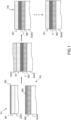
- HS hybrid systems are made as described figure 1 .
- first part P1 ensuring a first functionality, for example detection or emission, produced in one (or more) first material M1 on a substrate Subi
- second part P2 ensuring a second functionality, for example a silicon circuit allowing the reading or generation of electrical signals, made in a second material M2 different from the first material M1 and supported by a substrate Sub2.
- M3 material There is a layer of M3 material on each of them which will be used to carry out the assembly.
- These two parts are of planar structure, and have a “large surface”, that is to say typically 1 mm 2 or more. Then the two parts are assembled with one another by an assembly process, the material M3 making it possible to form the assembly layer 11. This step is also called hybridization.
- a rapidly developing assembly technique is collage. It constitutes significant progress for the achievement of so-called “above IC” technological steps, that is to say steps that can be carried out directly on the plate of the circuit forming one of the parts, typically of the CMOS type, and in a manner collective on all the chips.
- This compatibility with CMOS manufacturing means is adapted to a significant reduction in production costs and the possibility of achieving finer-sized technological patterns.
- bonding is molecular bonding.
- This method consists of specifically preparing the surface of the two parts with, as M3, a deposit of a dielectric material, typically silica, then carrying out planarizations. They are then brought into contact mechanically, then thermal annealing is carried out (around 200°C).
- the final assembly layer 11, for example SiO 2 has a thin thickness, typically from a few tens of nm to a few ⁇ m.
- one of the substrates is generally removed. In certain cases, the remaining substrate is also removed, to replace it with a Subd destination substrate, less expensive and/or having better mechanical or other properties (low dielectric losses).
- the assembly step is a high-risk step, and the inventors have demonstrated certain negative effects induced by bonding on hybrid detectors.
- An aim of the present invention is to remedy the aforementioned drawbacks by proposing a hybrid system having improved assembly quality.
- the present invention relates to a hybrid optical and/or electronic system as defined in claim 1.
- a depth of a recess is such that a bottom of said recess is placed at a distance from the assembly layer less than 1 ⁇ m.
- the recesses have the shape of holes or grooves.
- the recesses are covered with a metallic layer.
- the material of the hollowed-out planar structure has a coefficient of thermal expansion greater than the coefficient of thermal expansion of the other planar structure.
- the hollowed-out planar structure has a thickness of less than 20 ⁇ m.
- the assembly is carried out by molecular bonding.
- a surface of the at least one active zone is greater than or equal to 1 mm 2 .
- the first structure comprises in at least one layer a plurality of doped zones configured to collect carriers photogenerated by the absorbent layer, a doped zone making it possible to define a pixel of the detection system, in which the electrical signal is generated by a pixel at from said carriers photogenerated by the absorbent layer, an electrical connection between a doped zone and a buried contact of the reading circuit being made via holes metallized interconnections, and in which the hollowed-out planar structure is that which is crossed by the interconnections holes.
- the second structure is arranged on the rigid substrate, in which the interconnection holes pass through the first structure and the reading circuit to the contact, in which each doped zone extends in an annular manner around a via, the hollowed-out planar structure being the first planar structure.
- a depth of a recess is such that said recess does not reach the reading circuit.
- the recesses are made in the neutral zone arranged between a common contact and contact pads of said system.
- a first plurality of recesses are interconnected so as to form a test pad and a second plurality of recesses are connected to each other and to said common contact of the pixel matrix.
- the first planar structure is arranged on the rigid substrate, said rigid substrate being transparent, each doped zone (DZ) is produced in a contact layer (CL) placed under the absorbent layer (AL), the second planar structure (S2) is arranged on a thinned substrate (Sub'), the via holes (IH) pass through the thinned substrate (Sub') and the second planar structure (S2), the hollowed-out planar structure being the second planar structure , the recesses being made in the thinned substrate Sub' and the second planar structure S2.
- the invention relates to an optoelectronic display system comprising a matrix of electroluminescent pixels, in which the first functionality is pixelated emission, the first planar structure comprising a plurality of layers including an electroluminescent layer, in which the second functionality is a generation of electrical signals adapted to carry out the electroluminescent emission, the second planar structure comprising a pixel addressing circuit deposited on a silicon substrate, and in which the at at least one active zone comprises said matrix of pixels and the at least one neutral zone is arranged at the periphery of said matrix of pixels, the recessed structure corresponding to the first planar structure.
- the invention relates to an electronic system in which the first planar structure comprises a plurality of transistors and the second planar structure comprises circuits associated with said transistors, and in which the at least one active zone comprises said transistors and the at least one neutral zone is arranged at the periphery of said transistors, the hollow structure corresponding to the first planar structure.
- system further comprises CV interconnection vias in the active zone.
- the invention relates to a method of manufacturing a hybrid optical and/or hybrid electronic system as defined in claim 19.
- the inventors have particularly studied hybrid detectors using interconnection vias to connect the detection elements and the reading circuit. This study made it possible to highlight the appearance of “bubbles” and, following the analysis of this phenomenon, to propose a solution to eliminate them.
- Two types of hybrid via interconnect detectors based on III-V technology are described below. They operate in the infrared range and are formed by assembling a matrix comprising a plurality of elementary pixels based on photodiodes transforming a flow of incident photons into photogenerated carriers, and a reading circuit commonly called ROIC for “Read Out Integrated Circuit” in English to collect the electrical signal from the pixels of the detector.
- ROIC Read Out Integrated Circuit
- a first type of detector comprises via-holes and symmetry photodiodes cylindrical around these via holes. This photodiode is commonly called a “loop-hole”. We thus create an infrared imager by coupling 3D interconnection (ROIC circuit) and cylindrical photodiode.
- ROIC circuit 3D interconnection
- a hybrid optical detector 20 presenting a matrix of “loop hole” type photodiodes adapted for an absorbing structure made with III-V materials is illustrated figure 2 , Figure 2a corresponding to a cross section and Figure 2b to a top view.
- the photodetector matrix comprises an absorbing structure Sabs comprising at least one absorbing layer AL made of III-V or II-VI material, capable of generating PC carriers from a flow of incident photons F.
- the Sabs structure is covered with a Pass passivation layer. This structure is assembled to the ROIC circuit by an assembly layer 11, according to the method described above.
- the contacts of the ROIC reading circuit intended to receive the electrical signal generated by each Pix pixel of the detector are buried TLC contacts called “Top Level Contacts” in English. They are made at the end of the integrated circuit manufacturing process, and are located close to the surface of the circuit.
- a cylindrical diode PhD is produced around an interconnection hole IH (for “Interconnection Hole” in English), which passes through the absorbing structure, the assembly layer 11 and the ROIC circuit until the TLC contact.
- the walls of the hole IH are covered with a layer of metallization ML, creating the electrical connection between the diode PhD and the contact TLC.
- the diode PhD is produced by localized doping of a zone DZ close to the hole IH of a type opposite to the initial doping of the absorbing layer AL.
- the p-n type photodiode carries out the separation and transport of the photo-generated carriers to the ML metallization layer and collects the minority carriers (the holes when the DZ zone is p-doped).
- Each DZ doped zone which extends in an annular manner around an IH via hole makes it possible to define a Pix pixel of the detector, and the metallized IH holes make an electrical connection between DZ and the TLC contact.
- the document WO2013079603 describes a method of manufacturing a detector 20 based on “loop hole” diodes as described above, with an AL absorbent layer in III-V material.
- An example is an n-doped InGaAs absorber layer placed between two InP encapsulation layers.
- the document detector 20 WO2013079603 features a specific illumination configuration through the substrate, and a dual Visible/IR imager.
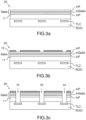
- a Sabs semiconductor structure comprising the absorbing layer AL between two barrier layers is assembled by bonding, via an assembly layer 11, to a ROIC reading circuit having TLC buried contacts. Then a masking dielectric 12 is deposited on the Sabs structure, and part of the masking dielectric layer is etched facing the TLC contacts as shown. figure3b .
- the IH via holes are made by vertical etching up to the TLC contacts, through the absorbent structure and the assembly layer as illustrated figure 3c . Engraving is carried out by dry or wet method.
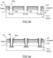
- a DZ doped zone for example p-type, is produced by diffusion or ion implantation of a Dop dopant via each IH hole, so as to form a PhD photodiode comprising a cylindrical pn junction. Diffusion takes place from the surface of the walls of the hole IH, and in parallel through all the layers composing the absorbent structure.
- a metallic layer ML is deposited on the walls of the holes IH so as to bring the doped zone DZ and the contact TLC into electrical contact.
- the IH interconnection holes are not made so as to pass through the absorbent structure as in the “loop hole” structure but pass through the CMOS type ROIC read circuit.
- TSV for “Through Silicon Via” in English. This type of detector is described in the patent application FR3053838 A1 .
- the Sabs absorbent structure deposited on a Sub substrate, comprises in this case: an active absorbent layer AL, an interface layer IL deposited between the substrate and the active layer, the role of which is to ensure good common electrical contact while by limiting the generation of dark current; a barrier layer BL deposited on the absorbent layer and a contact layer CL, deposited on the barrier layer, comprising the DZ doped zones.
- the overall thickness of the structure along the stacking direction is between 0.5 and 10 ⁇ m.
- the diode is created by stacking vertical layers, in particular by using a barrier, without needing doping to manufacture the diode (unlike Loop hole technology) but only to define the contact.
- the gap of the active layer is most often lower than the gap of the substrate and lower than the gap of the interface layer.
- the IH interconnection holes are etched through the reading circuit.
- the initial silicon substrate on which the ROIC circuit was made was thinned (thinned substrate not shown).
- a step of finalizing the connections consists of making the contacts for each pixel by filling the IH holes with a metallic material and connecting this metal with the TLC contacts.
- the absorbent layer AL of the absorbent structure is made of a III-V alloy, but can also be a II-VI material such as HgCdTe.
- Examples of material constituting the AL layer are: InGaAs / InP; InAsSb; InAsSb/lnAs superlattice; InSb; GaSb/InAs superlattice; GaN; AlGaN, AllnN, AlGaAsSb; GaAs/AlGaAs or InGaAs/AllnAs multi-quantum wells.
- the material is chosen based on the length range of desired sensitivity wave.
- the materials of adjacent layers are matched to the material of the AL layer.
- Each layer making up the Sabs absorbent structure is, conventionally, in mesh agreement or in near mesh agreement with the adjacent layer(s).
- the absorbent structure is produced by epitaxy of the layers on an initial Sub substrate.
- the Sub substrate of the Figure 4 is not the initial substrate. This has been removed and replaced by a more rigid substrate with improved mechanical strength, for example silicon or any other rigid material used in technological processes for the industrial manufacturing of integrated circuits. This replacement step is carried out once the absorbent structure is stuck to the reading circuit (see figure 1 ).
- HS hybrid systems for example detectors or displays, present a set of Pix pixels often arranged in a matrix, as illustrated. figure 5 .
- the HS hybrid system then has a central active zone Zact, that is to say functional, and on the periphery a non-functional zone Zn.
- a “loop-hole” photodiode matrix for an imager requires the production over a large surface area (>1 mm 2 ) of a large number of homogeneous pixels and their connections to the reading circuit. These pixels are produced by etching connection vias of diameter d1, then by diffusion of zinc at around 400°C in order to locally dope each via. In addition, other stages of the process (for the “loop hole” or the TSV) are likely to be carried out at temperatures of this order of magnitude: deposition of a dielectric, activation annealing, contact annealing, etc. .
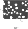
- the inventors have noticed that during a temperature rise above 300°C of the bonded hybrid structure, the transferred layer of III-V material (material M1) can become detached from the reading circuit (material M2: silicon) deposited on a Sub substrate (also silicon if not replaced), as shown Figure 6 .
- This separation can go until the local bursting of M1, leaving areas devoid of M1 material.
- the white bubbles 70 correspond to areas which have lost the M1 material, and the bubble 71 corresponds to an area with detached and stressed M1 material. These bubbles typically have a diameter of between 10 and 100 ⁇ m.
- neutral zones are zones without structure, without pattern, that is to say without spatially delimited layers. This does not mean that these areas are useless for the reading circuit, only these surfaces do not have a “top level” pattern for connection to the absorbent structure or to the final connections of the components. There are electronic structures/components at deeper levels. And we see that bubbles appear on all these surfaces, significantly degrading the quality of the photolithography steps, the matrix and ultimately its performance.
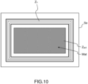
- a hybrid system 10 according to the invention is illustrated in section figure 8 , and in top view Figure 9 , on the side presenting the holes of depth Pe.
- the hybrid system 10 according to the invention is optical and/or electronic as explained above.
- first planar structure S1 having a first functionality made in at least a first material M1 and a second planar structure S2 having a second functionality made in at least a second material M2 different from the first material.
- the corresponding structure can be made up of a plurality of layers of different materials but in mesh agreement, such as InP/InGaAs/InP.
- the most common variant is a circuit made in silicon
- the first and second planar structures are assembled by an assembly layer 11, at least one of the planar structures being arranged on a rigid substrate Sub.
- the Sub substrate is then also silicon (if it has not been replaced).
- the hybrid system 10 comprises at least one active zone Zact used to implement the functionalities, and at least one neutral zone Zn not used to implement these functionalities and arranged on the periphery of said active zone.
- the hybrid system is preferably “large surface”, that is to say with a central useful zone surface of at least 1 mm 2 .
- the system further comprises recesses Ev made in at least one neutral zone Zn of the planar structure which is not arranged on the rigid substrate, called hollowed-out planar structure Se.
- the recesses are arranged in non-functional areas and on the periphery, and therefore do not disrupt the operation of the system. These are simple “holes” that have no electrical functionality. Their function is to allow degassing and/or relaxation of thermal stresses in order to reduce or even eliminate the bubbles previously described.
- the recesses are preferably made in the thinnest Se structure, that is to say the one which is not placed on the rigid substrate Sub which supports the system.
- the hollowed-out planar structure has a thickness of less than 20 ⁇ m.
- the depth Pe of the recesses depends on the thickness of the structure Se, and this thickness can vary between 1 ⁇ m and 20 ⁇ m.
- the depth Pe of the recesses Ev is such that a bottom of said recess is placed at a distance “from” the assembly layer of less than 1 ⁇ m.
- the inventors have shown that it is not necessary to obtain the suppression of bubbles that the recess reaches the assembly layer 11, it is enough to get close enough to obtain the desired effect. This makes it possible to make shallower recesses which do not risk damaging the structure below, such as a circuit component.
- the recesses When the recesses are made in detectors using IH interconnection vias, they can be made during the etching step of these vias. They will then undergo all the other stages of the process, and therefore in this variant the recesses are metallized, that is to say covered with a metallic layer, like the IH.
- the material of the hollowed planar structure has a coefficient of thermal expansion greater than the coefficient of thermal expansion of the other planar structure.
- the assembly is carried out by molecular bonding.
- the assembly layer then preferably comprises silica.
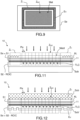
- FIG. 11 illustrates a first variant of an optoelectronic detection system 10 according to the invention comprising a matrix of pixels Matd.
- the first functionality is a pixelated photo-generation of carriers, the first structure S1 comprising a plurality of layers including an absorbing layer AL of II-VI or III-V semiconductor material, and in which the second functionality is a reading of a signal generated by a pixel, the second structure S2 comprising a read circuit ROIC which includes buried TLC contacts.
- An active zone Zact comprises the matrix of pixels Matd and a neutral zone Zn is arranged on the periphery of the matrix of pixels.
- the recesses are made in the first structure, and the substrate Sub is the substrate of the ROIC circuit, typically made of silicon.
- FIG. 12 illustrates a second variant of an optoelectronic detection system 10 according to the invention comprising a matrix of pixels Matd.
- the rigid Sub substrate is here the substrate of the detection layers, either the initial InP substrate or a replacement substrate, such as silicon.
- the recesses are made in the second ROIC structure, and the recesses pass through the thinned silicon substrate Sub' of the ROIC circuit and at least part of the circuit itself.
- the first structure S1 of the hybrid optoelectronic detection system comprises in at least one layer a plurality of doped zones DZ configured to collect carriers photogenerated by the absorbing layer, a doped zone allowing you to define a Pix pixel of the detection system.
- the electrical signal is then generated by a pixel from the carriers photogenerated by the absorbing layer AL, and the electrical connection between a doped zone DZ and a buried TLC contact of the ROIC read circuit is made via metallized IH interconnection holes.
- the hollowed-out planar structure Se is then preferentially that which is crossed by the interconnection holes IH.
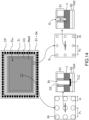
- a hybrid detection system 10 of the “loop hole” type according to the first variant and according to the embodiment above is illustrated Figure 13 .
- the second structure S2 is arranged on the rigid substrate Sub, the via holes IH pass through the first structure S1, the assembly layer and the read circuit ROIC up to the contact TLC.
- Each doped zone DZ extends annularly around a via hole IH, and the hollowed-out planar structure Se is the first planar structure S1.
- the active zone of the detection system 10 comprises the Matd matrix of Pix pixels and also includes a common contact CC around the matrix.
- the system thus presents a non-functional neutral zone Zn between the common contact CC and the connection pads CP in which the recesses Ev are made.
- the depth pe of a recess Ev is such that it does not reach the ROIC reading circuit, so as not to risk damaging it.
- the vias IH are circular holes which have a diameter d1 and a depth p1 and the recesses Ev are also circular holes which therefore have a depth p2 ⁇ p1 and a diameter d2 ⁇ d1.
- the depth of the vias decreases with their diameter, and therefore if we wish to obtain a depth d2 ⁇ d1, d2 must be less than d1.
- Ev holes are preferably made at the same time as the via IH for Loop-hole. Their production does not require specific lithography or an engraving step.
- the diameter d1 of the vias IH is chosen so that the depth p1 is such that IH leads to the “top metal” level (case of pixels), and the diameter d2 of the holes Ev is chosen so that the depth p2 is such that Ev emerges at the level of the bonding silica (in the areas without pixels). Non-pixelated areas are not covered at “top-metal” level.
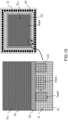
- the Ev holes made at the same time as the IH vias, also have a DZ doped zone and a metallization (not shown Figure 14 ).
- a second advantage of this embodiment is that the surfaces which were free (without via), will then undergo the same mechanisms of manufacturing, and homogenize the surface of the matrix during manufacturing steps requiring the intervention of reactive species (plasma etching, dopant diffusion). We then obtain better pixel homogeneity of the matrix by reducing the differences between edge and center of the matrix.
- a hybrid detection system 10 of the TSV type according to the second variant is shown Figure 16 .
- the via holes IH pass through the thinned substrate Sub' and the second planar structure S2.
- the recesses Ev are made on the reading circuit side, through the thinned silicon substrate Sub'.
- the hollowed-out planar structure Se is here the second planar structure S2.
- the rigid substrate Sub here placed on the side of the incident light rays, must then be transparent in the spectral band of interest.
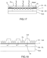
- the hybrid system 10 is an optoelectronic display system comprising a matrix of Matel electroluminescent pixels, as illustrated Figure 17 , for example of the LED microdisplay type.
- the first functionality is pixelated emission
- the first planar structure S1 comprises a plurality of layers including an EL electroluminescent layer.
- the second functionality is a generation of electrical signals adapted to carry out the electroluminescent emission, the second planar structure S2 comprising an AC pixel addressing circuit deposited on a Sub substrate, preferably made of silicon.
- the at least one active zone Zact comprises the matrix of pixels Mael and the at least one neutral zone Zn is arranged on the periphery of said matrix of pixels.
- the hollowed-out structure corresponds to S1.
- the hybrid system 10 is a fast electronic system illustrated Figure 18 , resulting from the heterogeneous integration of III-V materials on a CMOS circuit on silicon.
- the first planar structure S1 comprises a plurality of transistors T and the second planar structure S2 comprises Cire circuits associated with said transistors.
- the active zone Zact comprises the transistors T and the neutral zone Zn in which the recesses are made is arranged at the periphery of the transistors, the hollowed-out structure Se corresponding to the first planar structure S1.
- the first material for the transistors is for example GaN, InP or GaAs and the second material for the circuits is for example silicon.
- Bipolar hetero-structure transistors in InGaAs/InP make it possible to perform fast analog conversion functions up to a few tens of GHz.
- InP bonding on a CMOS circuit makes it possible to associate fast functions on InP and digital functions on CMOS.
- the Zact active zone includes interconnection holes or CV connection vias taking various shapes, to evacuate the bubbles which could form in this zone.
- degassing vias that is to say recesses Ev
- electrical connection vias CV base, emitter collector in the case of a bipolar transistor, gate, drain, source in the case of a field effect transistor
- CV base, emitter collector in the case of a bipolar transistor, gate, drain, source in the case of a field effect transistor
- the first functionality is an individualized laser emission
- the first planar structure S1 comprising a plurality of laser emitters Las
- the second functionality is a processing of the optical beams FI generated by the Las laser transmitters.
- the second planar structure S2 comprises at least one optical processing layer OL deposited on the rigid substrate Sub.
- the laser transmitters are configured to transmit towards the OL layer.
- the processing layer(s) perform guidance functions, multiplexing/demultiplexing, filtering, amplification, etc.
- the recesses are made in the areas that have not been eliminated during the manufacturing of the laser ribbons. These are non-functional areas, but which could have been kept in order to protect the underlying circuit. Recesses are made in areas where there is no laser tape but there is still carryover material.
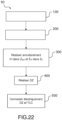
- the invention relates to a method 50 for manufacturing a hybrid optical and/or electronic hybrid system, illustrated Figure 20 .
- the method comprises a first step 100 consisting of assembling by an assembly layer 11 on the one hand a first planar structure S1 having a first functionality made in at least a first material M1, S1 being deposited on a first substrate Subi, and d on the other hand a second planar structure S2 having a second functionality made in at least a second material M2 different from the first material, S2 being deposited on a second substrate Sub2.
- the first and second assembled structures comprise at least one active zone (Zact) used to implement said functionalities, and at least one neutral zone (Zn) not used to implement said functionalities.
- the method 50 further comprises a step 250 of replacing the remaining substrate Sub1 or Sub 2 with a destination substrate Subd (see figure 1 ).
- a third step 300 recesses Ev are made in at least one neutral zone Zn of the planar structure which is not arranged on the rigid substrate Sub, called hollowed-out planar structure Se.
- the step 300 of producing the recesses consists of simultaneously producing interconnection holes IH or CV in the at least one active zone Zact through one of the planar structures, and the recesses Ev in the at least one Zn neutral zone of said planar structure crossed by the interconnection holes.
- the hollowed-out structure is the one through which the connection holes are made.
- the step of simultaneously producing the interconnection holes IH, CV and/or the recesses Ev is carried out by lithography then engraving.
- the lithography technology is chosen from: by electron beam; by nanoimprinting; by optical lithography.
- the engraving technology is chosen from ion etching, chemical etching, plasma etching.
- the method 50 produces a hybrid optoelectronic detector comprising a matrix of Matd pixels.
- the first functionality here is a pixelated photo-generation of carriers, the first structure S1 comprising a plurality of layers including an absorbing layer AL in II-VI or III-V semiconductor material.
- the second functionality being a reading of a signal generated by a pixel
- the second structure S2 comprising a reading circuit ROIC intended to recover an electrical signal from said photo-generated carriers by the absorbent layer AL and comprising a plurality of TLC contacts buried.
- the at least one active zone Zact comprises the matrix of pixels, and the at least one neutral zone Zn is arranged on the periphery of said matrix of pixels.
- step 300 of producing the recesses consists of simultaneously producing interconnection holes IH in the at least one active zone Zact through one of the planar structures, and the recesses Ev in the at least one Zn neutral zone of said planar structure crossed by the interconnection holes.
- the method 50 for manufacturing a hybrid optoelectronic detector further comprises the following steps, carried out after step 300:
- a step 400 a plurality of doped zones DZ are produced, configured to collect carriers photogenerated by the absorbent layer, a doped zone making it possible to define a Pix pixel of the detector.
- each doped zone DZ is electrically connected with the associated contact TLC of the read circuit ROIC via the interconnection holes IH.
- the method 50 according to the invention produces a “loop hole” detector.
- the step 300 of simultaneously producing the interconnection holes and the recesses is carried out by etching the first planar structure S1 and, for the interconnection holes, from the reading circuit ROIC to the buried contacts TLC.
- the hollowed-out planar structure here corresponds to the first planar structure.
- the method 50 according to the invention produces a TSV detector.
- the step 300 of simultaneously producing the interconnection holes and the recesses is carried out by etching the thinned substrate Sub' on which the ROIC reading circuit is deposited and by etching, at least partially, the ROIC reading circuit.
- the hollowed planar structure corresponds here to the second structure S2.
Landscapes
- Solid State Image Pick-Up Elements (AREA)
- Glass Compositions (AREA)
- Optical Fibers, Optical Fiber Cores, And Optical Fiber Bundles (AREA)
- Optical Communication System (AREA)
- Light Receiving Elements (AREA)
Claims (25)
- Hybrides optisches und/oder elektronisches System (10), umfassend eine Pixelmatrix (Matd, Matel) und Folgendes umfassend:- eine erste planare Struktur (S1) mit einer ersten Funktionalität, die aus mindestens einem ersten Material (M1) hergestellt ist, wobei die erste Funktionalität eine pixelierte Photogeneration von Trägern oder eine pixelierte Elektrolumineszenzemission ist,- eine zweite planare Struktur (S2) mit einer zweiten Funktionalität, die aus mindestens einem zweiten Material (M2) hergestellt ist, das sich von dem ersten Material unterscheidet, wobei die zweite Funktionalität ein Lesen eines von einem Pixel erzeugten elektrischen Signals ist, wenn die erste Funktionalität eine pixelierte Photogeneration von Trägern ist, oder eine Erzeugung von elektrischen Signalen, die geeignet sind, die elektrolumineszente Emission zu bewirken, wenn die erste Funktionalität eine pixelierte elektrolumineszente Emission ist,- wobei die erste und die zweite planare Struktur durch eine Zusammenfügungsschicht (11) zusammengefügt sind, wobei mindestens eine der planaren Strukturen auf einem starren Substrat (Sub) angeordnet ist,- wobei das System mindestens einen aktiven Bereich (Zact) umfasst, der zur Implementierung der Funktionalitäten verwendet wird und die Pixelmatrix umfasst, und mindestens einen neutralen Bereich (Zn), der nicht zur Implementierung der Funktionalitäten verwendet wird und am Umfang des aktiven Bereichs angeordnet ist,- wobei das System ferner Aussparungen (Ev) umfasst, die in mindestens einem neutralen Bereich der planaren Struktur gebildet sind, der nicht auf dem starren Substrat angeordnet ist, der als ausgesparte planare Struktur (Se) bezeichnet wird, wobei der mindestens eine neutrale Bereich, in dem die Aussparungen gebildet sind, am Umfang der Pixelmatrix angeordnet ist und die Aussparungen (Ev) keine elektrische Funktionalität aufweisen.
- System nach Anspruch 1, wobei eine Tiefe einer Aussparung (pe) derart ist, dass ein Boden der Aussparung in einem Abstand (de) von der Zusammenfügungsschicht von weniger als 1 µm angeordnet ist.
- System nach einem der Ansprüche 1 oder 2, wobei die Aussparungen die Form von Löchern oder Rillen aufweisen.
- System nach einem der vorhergehenden Ansprüche, wobei die Aussparungen mit einer Metallschicht bedeckt sind.
- System nach einem der vorhergehenden Ansprüche, wobei das Material der ausgesparten planaren Struktur (Se) einen höheren Wärmeausdehnungskoeffizienten als der Wärmeausdehnungskoeffizient der anderen planaren Struktur aufweist.
- System nach einem der vorhergehenden Ansprüche, wobei die ausgesparte planare Struktur eine Dicke von weniger als 20 µm aufweist.
- System nach einem der vorhergehenden Ansprüche, wobei die Zusammenfügung durch molekulares Kleben hergestellt wird.
- System nach einem der vorhergehenden Ansprüche, wobei eine Fläche des mindestens einen aktiven Bereichs größer als oder gleich 1 mm2 ist.
- Optoelektronisches Detektionssystem (10) nach einem der vorhergehenden Ansprüche, umfassend eine Pixelmatrix (Matd),wobei die erste Funktionalität eine pixelierte Photogeneration von Trägern ist, wobei die erste Struktur (S1) eine Vielzahl von Schichten umfasst, darunter eine absorbierende Schicht (AL) aus II-VI oder III-V Halbleitermaterial,wobei die zweite Funktionalität ein Lesen eines von einem Pixel erzeugten elektrischen Signals ist, wobei die zweite Struktur (S2) eine Leseschaltung (ROIC) umfasst, die eine Vielzahl von vergrabenen Kontakten (TLC) aufweist,und wobei der mindestens eine aktive Bereich (Zact) die Pixelmatrix umfasst und der mindestens eine neutrale Bereich (Zn) am Umfang der Pixelmatrix angeordnet ist.
- Optoelektronisches Detektionssystem (10) nach Anspruch 9, wobei die erste Struktur (S1) in mindestens einer Schicht eine Vielzahl von dotierten Bereichen (DZ) umfasst, die so konfiguriert sind, dass sie von der absorbierenden Schicht photogenerierte Träger sammeln, wobei ein dotierter Bereich ein Pixel (Pix) des Detektionssystems definieren kann, wobei das elektrische Signal von einem Pixel aus den von der absorbierenden Schicht (AL) photogenerierten Trägern erzeugt wird, wobei eine elektrische Verbindung zwischen einem dotierten Bereich (DZ) und einem vergrabenen Kontakt (TLC) der Leseschaltung (ROIC) über metallisierte Durchkontaktierungslöcher (IH) hergestellt wird, und wobei die ausgesparte planare Struktur (Se) diejenige ist, die von den Durchkontaktierungslöchern durchquert wird.
- Optoelektronisches Detektionssystem (10) nach Anspruch 10, wobei die zweite Struktur (S2) auf dem starren Substrat (Sub) angeordnet ist, wobei die Durchkontaktierungslöcher (IH) durch die erste Struktur (S1) und die Leseschaltung (ROIC) bis zum Kontakt (TLC) verlaufen, wobei jeder dotierte Bereich (DZ) sich ringförmig um ein Durchkontaktierungsloch erstreckt, wobei die ausgesparte planare Struktur (Se) die erste planare Struktur (S1) ist.
- Optoelektronisches Detektionssystem (10) nach einem der Ansprüche 10 oder 11, wobei eine Tiefe einer Aussparung (Pe) derart ist, dass die Aussparung die Leseschaltung nicht erreicht.
- Optoelektronisches Erfassungssystem (10) nach einem der Ansprüche 9 bis 12, wobei die Aussparungen in dem neutralen Bereich (Zn) ausgeführt sind, der zwischen einem gemeinsamen Kontakt (CC) und Kontaktpads (CP) des Systems angeordnet ist.
- Optoelektronisches Detektionssystem (10) nach Anspruch 13, wobei eine erste Vielzahl von Aussparungen miteinander verbunden ist, um ein Testpad (TestP) zu bilden, und wobei eine zweite Vielzahl von Aussparungen miteinander und mit dem gemeinsamen Kontakt (CC) der Pixelmatrix (Matd) verbunden ist.
- Optoelektronisches Detektionssystem nach einem der Ansprüche 9 oder 10, wobei die erste planare Struktur (S1) auf dem starren Substrat (Sub) angeordnet ist, wobei das starre Substrat transparent ist, wobei jeder dotierte Bereich (DZ) in einer Kontaktschicht (CL) gebildet ist, die unterhalb der absorbierenden Schicht (AL) angeordnet ist,wobei die zweite planare Struktur (S2) auf einem ausgedünnten Substrat (Sub') angeordnet ist,wobei die Durchkontaktierungslöcher (IH) durch das ausgedünnte Substrat (Sub') und die zweite planare Struktur (S2) verlaufen, wobei die ausgesparte planare Struktur (Se) die zweite planare Struktur (S2) ist, wobei die Aussparungen in dem ausgedünnten Substrat (Sub') und der zweiten planaren Struktur (S2) gebildet sind.
- Optoelektronisches Anzeigesystem nach einem der Ansprüche 1 bis 8, umfassend eine Matrix aus elektrolumineszenten Pixeln (Matel)wobei die erste Funktionalität eine pixelierte Emission ist, wobei die erste planare Struktur (S1) eine Vielzahl von Schichten umfasst, einschließlich einer elektrolumineszierenden Schicht,wobei die zweite Funktionalität eine Erzeugung von elektrischen Signalen ist, die geeignet sind, die Elektrolumineszenzemission zu realisieren, wobei die zweite planare Struktur (S2) eine auf einem Siliziumsubstrat aufgebrachte Pixeladressierungsschaltung (AC) umfasst, und wobei der mindestens eine aktive Bereich (Zact) die Pixelmatrix (Matel) umfasst und der mindestens eine neutrale Bereich (Zn) am Umfang der Pixelmatrix angeordnet ist, wobei die ausgesparte Struktur (Se) der ersten planaren Struktur (S1) entspricht.
- Elektronisches System nach einem der Ansprüche 1 bis 8, wobei die erste planare Struktur (S1) eine Vielzahl von Transistoren (T) umfasst und die zweite planare Struktur Schaltungen (Circ) umfasst, die den Transistoren zugeordnet sind, und wobei der mindestens eine aktive Bereich (Zact) die Transistoren umfasst und der mindestens eine neutrale Bereich (Zn) am Umfang der Transistoren angeordnet ist, wobei die ausgesparte Struktur (Se) der ersten planaren Struktur (S1) entspricht.
- System nach einem der Ansprüche 16 oder 17, ferner umfassend Durchkontaktierungslöcher (CV) in dem aktiven Bereich.
- Verfahren (50) zur Herstellung eines hybriden optischen und/oder elektronischen Systems, wobei das Verfahren die folgenden Schritte umfasst:- Zusammenfügen (100), durch eine Zusammenfügungsschicht (11), einer ersten planaren Struktur (S1), die eine erste Funktionalität aufweist und eine Pixelmatrix umfasst, die aus mindestens einem ersten Material (M1) hergestellt ist, wobei die erste Funktionalität eine pixelierte Photogeneration von Trägern oder eine pixelierte elektrolumineszente Emission ist, wobei die erste Struktur (S1) auf einem ersten Substrat (Sub1) abgelagert wird, und einer zweiten planaren Struktur (S2), die eine zweite Funktionalität aufweist, die aus mindestens einem zweiten Material (M2) hergestellt ist, das sich von dem ersten Material unterscheidet, wobei die zweite Struktur (S2) auf einem zweiten Substrat (Sub2) abgelagert wird, wobei die zweite Funktionalität ein Lesen eines von einem Pixel erzeugten elektrischen Signals ist, wenn die erste Funktionalität eine pixelierte Photogeneration von Trägern ist, oder eine Erzeugung von elektrischen Signalen, die geeignet sind, die elektrolumineszente Emission zu realisieren, wenn die erste Funktionalität eine pixelierte elektrolumineszente Emission ist,
wobei die erste und die zweite zusammengesetzte Struktur mindestens einen aktiven Bereich (Zact) umfassen, der zur Implementierung der Funktionalitäten verwendet wird, und mindestens einen neutralen Bereich (Zn), der nicht zur Implementierung der Funktionalitäten verwendet wird, wobei der aktive Bereich die Pixelmatrix umfasst,- Ablösen (200) eines der Substrate, sodass nur ein einziges starres Substrat (Sub1, Sub2) erhalten bleibt,- Herstellen (300) von Aussparungen (Ev) in mindestens einem neutralen Bereich (Zn) der planaren Struktur, der nicht auf dem starren Substrat angeordnet ist, genannt ausgesparte planare Struktur (Se), wobei der mindestens eine neutrale Bereich, in dem die Aussparungen hergestellt werden, am Umfang der Pixelmatrix angeordnet ist und die Aussparungen keine elektrische Funktionalität haben. - Verfahren (50) nach Anspruch 19, ferner umfassend einen Schritt (250) des Ersetzens des verbleibenden Substrats durch ein Zielsubstrat (Subd).
- Verfahren (50) nach einem der Ansprüche 19 oder 20 zur Herstellung eines hybriden optoelektronischen Detektors, der eine Pixelmatrix (Matd) umfasst,wobei die erste Funktionalität eine pixelierte Photogeneration von Trägern ist, wobei die erste Struktur (S1) eine Vielzahl von Schichten umfasst, darunter eine absorbierende Schicht (AL) aus II-VI- oder III-V-Halbleitermaterial,wobei die zweite Funktionalität ein Lesen eines von einem Pixel erzeugten Signals ist, wobei die zweite Struktur (S2) eine Leseschaltung (ROIC) umfasst, die dazu bestimmt ist, ein elektrisches Signal anhand der von der absorbierenden Schicht (AL) photogenerierten Träger abzugreifen, und die eine Vielzahl von vergrabenen Kontakten (TLC) umfasst,wobei der mindestens eine aktive Bereich (Zact) die Pixelmatrix umfasst, und der mindestens eine neutrale Bereich (Zn) am Umfang der Pixelmatrix angeordnet ist,wobei der Schritt der Herstellung der Aussparungen (300) darin besteht, gleichzeitig Durchkontaktierungslöcher (IH) in dem mindestens einen aktiven Bereich (Zact) durch eine der planaren Strukturen und die Aussparungen (Ev) in dem mindestens einen neutralen Bereich (Zn) der planaren Struktur, die von den Durchkontaktierungslöchern durchquert wird, zu bilden.
- Verfahren (50) zur Herstellung nach einem der Ansprüche 19 bis 21 eines hybriden optoelektronischen Detektors, ferner folgende Schritte umfassend:- Herstellen (400) einer Vielzahl von dotierten Bereichen (DZ), die so konfiguriert sind, dass sie von der absorbierenden Schicht photogenerierte Träger sammeln, wobei ein dotierter Bereich zur Definition eines Pixels (Pix) des Detektors dient,- elektrisches Verbinden (500) jedes dotierten Bereichs (DZ) mit dem zugeordneten Kontakt (TLC) der Leseschaltung (ROIC) über die Durchkontaktierungslöcher (IH).
- Verfahren nach einem der Ansprüche 21 bis 22, wobei der Schritt der gleichzeitigen Herstellung der Durchkontaktierungslöcher und der Aussparungen durch Ätzen der ersten planaren Struktur (S1) und, für die Durchkontaktierungslöcher, der Leseschaltung (ROIC) bis zu den vergrabenen Kontakten (TLC) erfolgt, wobei die ausgesparte planare Struktur der ersten planaren Struktur entspricht.
- Verfahren nach einem der Ansprüche 21 bis 22, wobei der Schritt der gleichzeitigen Herstellung der Durchkontaktierungslöcher und der Aussparungen durch Ätzen des ausgedünnten Substrats (Sub'), auf dem die Leseschaltung abgelagert ist, und mindestens teilweise der Leseschaltung (ROIC) erfolgt, wobei die ausgesparte planare Struktur der zweiten Struktur entspricht.
- Verfahren nach einem der Ansprüche 21 bis 24, wobei der Schritt der gleichzeitigen Herstellung der Durchkontaktierungslöcher (IH) und der Aussparungen (Ev) durch Lithografie und anschließendes Ätzen erfolgt, wobei die Lithografietechnologie ausgewählt ist aus: Elektronenstrahl; Nanoprint; optischer Lithografie, und die Ätztechnologie ausgewählt ist aus Ionenätzen, chemischem Ätzen oder Plasmaätzen.
Applications Claiming Priority (2)
| Application Number | Priority Date | Filing Date | Title |
|---|---|---|---|
| FR1701175A FR3073668B1 (fr) | 2017-11-14 | 2017-11-14 | Systeme optique/electronique hybride ameliore |
| PCT/EP2018/081093 WO2019096794A1 (fr) | 2017-11-14 | 2018-11-13 | Systeme optique/electronique hybride ameliore |
Publications (2)
| Publication Number | Publication Date |
|---|---|
| EP3711096A1 EP3711096A1 (de) | 2020-09-23 |
| EP3711096B1 true EP3711096B1 (de) | 2024-03-27 |
Family
ID=61258280
Family Applications (1)
| Application Number | Title | Priority Date | Filing Date |
|---|---|---|---|
| EP18796993.6A Active EP3711096B1 (de) | 2017-11-14 | 2018-11-13 | Verbessertes hybrides optisches/elektronisches system |
Country Status (5)
| Country | Link |
|---|---|
| US (1) | US11482563B2 (de) |
| EP (1) | EP3711096B1 (de) |
| FR (1) | FR3073668B1 (de) |
| IL (1) | IL274636B2 (de) |
| WO (1) | WO2019096794A1 (de) |
Families Citing this family (1)
| Publication number | Priority date | Publication date | Assignee | Title |
|---|---|---|---|---|
| FR3069958B1 (fr) * | 2017-08-03 | 2019-08-30 | Thales | Procede de fabrication ameliore d'un detecteur optique a base de photodiodes et dispositif associe |
Family Cites Families (12)
| Publication number | Priority date | Publication date | Assignee | Title |
|---|---|---|---|---|
| FR1601066A (de) | 1966-06-18 | 1970-08-10 | ||
| JP5716347B2 (ja) * | 2010-10-21 | 2015-05-13 | ソニー株式会社 | 固体撮像装置及び電子機器 |
| FR2983348B1 (fr) * | 2011-11-29 | 2014-07-25 | Thales Sa | Bloc detecteur optique |
| JP6214132B2 (ja) * | 2012-02-29 | 2017-10-18 | キヤノン株式会社 | 光電変換装置、撮像システムおよび光電変換装置の製造方法 |
| US8766387B2 (en) * | 2012-05-18 | 2014-07-01 | Taiwan Semiconductor Manufacturing Company, Ltd. | Vertically integrated image sensor chips and methods for forming the same |
| US9559135B2 (en) * | 2014-08-20 | 2017-01-31 | Taiwan Semiconductor Manufacturing Company Ltd. | Conduction layer for stacked CIS charging prevention |
| KR102274775B1 (ko) * | 2014-11-13 | 2021-07-08 | 삼성전자주식회사 | 반도체 장치 및 그 제조 방법 |
| US9666619B2 (en) * | 2015-04-16 | 2017-05-30 | Taiwan Semiconductor Manufacturing Co., Ltd. | CMOS image sensor structure |
| US10038026B2 (en) * | 2015-06-25 | 2018-07-31 | Taiwan Semiconductor Manufacturing Co., Ltd. | Bond pad structure for bonding improvement |
| KR20180074671A (ko) * | 2015-08-31 | 2018-07-03 | 쥐-레이 스위츨란드 에스에이 | 모놀리식 cmos 통합된 픽셀 검출기가 구비된 광자 계측용 콘빔 ct 장치 |
| US9773829B2 (en) * | 2016-02-03 | 2017-09-26 | Omnivision Technologies, Inc. | Through-semiconductor-via capping layer as etch stop layer |
| FR3053838B1 (fr) | 2016-07-08 | 2018-08-17 | Thales | Procede de fabrication de photodetecteur comprenant un empilement de couches superposees |
-
2017
- 2017-11-14 FR FR1701175A patent/FR3073668B1/fr active Active
-
2018
- 2018-11-13 EP EP18796993.6A patent/EP3711096B1/de active Active
- 2018-11-13 US US16/763,549 patent/US11482563B2/en active Active
- 2018-11-13 WO PCT/EP2018/081093 patent/WO2019096794A1/fr not_active Ceased
- 2018-11-13 IL IL274636A patent/IL274636B2/en unknown
Also Published As
| Publication number | Publication date |
|---|---|
| EP3711096A1 (de) | 2020-09-23 |
| FR3073668B1 (fr) | 2022-04-22 |
| IL274636B2 (en) | 2023-11-01 |
| FR3073668A1 (fr) | 2019-05-17 |
| IL274636B1 (en) | 2023-07-01 |
| US20200365631A1 (en) | 2020-11-19 |
| WO2019096794A1 (fr) | 2019-05-23 |
| US11482563B2 (en) | 2022-10-25 |
| IL274636A (en) | 2020-06-30 |
Similar Documents
| Publication | Publication Date | Title |
|---|---|---|
| EP3667728B1 (de) | Verfahren zur herstellung einer vorrichtung mit lichtemittierenden und/oder lichtempfangenden dioden und mit einem selbst ausgerichteten kollimationsgitter | |
| EP3893281B1 (de) | Lichtemittierende und/oder lichtempfangende diodenarray-vorrichtung | |
| EP2038929B1 (de) | Verfahren zur herstellung einer matrix aus einzelnen elektronischen komponenten und auf diese weise hergestellte matrix | |
| EP3780123B1 (de) | Verfahren zur herstellung elektronischer vorrichtungen | |
| FR3089348A1 (fr) | procede de fabrication d’une matrice de diodes a base de germanium et a faible courant d’obscurité | |
| EP4092746A1 (de) | Verfahren zur herstellung einer optoelektronischen vorrichtung | |
| EP1756872B1 (de) | Mesastruktur-photonerkennungschaltung | |
| EP3711096B1 (de) | Verbessertes hybrides optisches/elektronisches system | |
| EP3662512B1 (de) | Verfahren zur verbesserten herstellung eines photodiodenbasierten optischen sensors und zugehörige vorrichtung | |
| EP3662511B1 (de) | Verbesserter infrarotdetektor | |
| EP4268281B1 (de) | Integration einer detektionsschaltung auf der basis von optischen resonatoren, die mit einer ausleseschaltung eines bildaufnehmers verbunden sind | |
| EP4268282B1 (de) | Integration einer detektionsschaltung auf der basis von optischen resonatoren auf einer ausleseschaltung eines bildaufnehmers | |
| EP4383338B1 (de) | Verfahren zur herstellung einer optoelektronischen vorrichtung mit einer led und einer photodiode | |
| EP4525587A1 (de) | Abbildungsarray mit konvexen photodioden | |
| EP4621847A1 (de) | Optoelektronische vorrichtung mit einer lichtemittierenden diode, die mit einem photodetektor überlagert ist | |
| EP4358156A1 (de) | Verfahren zur herstellung von strahlungsgehärteten heteroübergangsphotodioden | |
| FR3094141A1 (fr) | procede de fabrication d’un composant optoelectronique a transmission optique en face arriere | |
| WO2020094944A1 (fr) | Procede de fabrication collective d'une pluralite de structures semi-conductrices | |
| WO2006000729A1 (fr) | Dispositif de prelevement d'une partie d'un faisceau lumineux issu d'un composant electronique emetteur de lumiere |
Legal Events
| Date | Code | Title | Description |
|---|---|---|---|
| STAA | Information on the status of an ep patent application or granted ep patent |
Free format text: STATUS: UNKNOWN |
|
| STAA | Information on the status of an ep patent application or granted ep patent |
Free format text: STATUS: THE INTERNATIONAL PUBLICATION HAS BEEN MADE |
|
| PUAI | Public reference made under article 153(3) epc to a published international application that has entered the european phase |
Free format text: ORIGINAL CODE: 0009012 |
|
| STAA | Information on the status of an ep patent application or granted ep patent |
Free format text: STATUS: REQUEST FOR EXAMINATION WAS MADE |
|
| 17P | Request for examination filed |
Effective date: 20200512 |
|
| AK | Designated contracting states |
Kind code of ref document: A1 Designated state(s): AL AT BE BG CH CY CZ DE DK EE ES FI FR GB GR HR HU IE IS IT LI LT LU LV MC MK MT NL NO PL PT RO RS SE SI SK SM TR |
|
| AX | Request for extension of the european patent |
Extension state: BA ME |
|
| DAV | Request for validation of the european patent (deleted) | ||
| DAX | Request for extension of the european patent (deleted) | ||
| STAA | Information on the status of an ep patent application or granted ep patent |
Free format text: STATUS: EXAMINATION IS IN PROGRESS |
|
| 17Q | First examination report despatched |
Effective date: 20230710 |
|
| GRAP | Despatch of communication of intention to grant a patent |
Free format text: ORIGINAL CODE: EPIDOSNIGR1 |
|
| STAA | Information on the status of an ep patent application or granted ep patent |
Free format text: STATUS: GRANT OF PATENT IS INTENDED |
|
| RIC1 | Information provided on ipc code assigned before grant |
Ipc: H01L 27/15 20060101ALI20231123BHEP Ipc: H01L 27/146 20060101AFI20231123BHEP |
|
| INTG | Intention to grant announced |
Effective date: 20231206 |
|
| GRAS | Grant fee paid |
Free format text: ORIGINAL CODE: EPIDOSNIGR3 |
|
| GRAA | (expected) grant |
Free format text: ORIGINAL CODE: 0009210 |
|
| STAA | Information on the status of an ep patent application or granted ep patent |
Free format text: STATUS: THE PATENT HAS BEEN GRANTED |
|
| AK | Designated contracting states |
Kind code of ref document: B1 Designated state(s): AL AT BE BG CH CY CZ DE DK EE ES FI FR GB GR HR HU IE IS IT LI LT LU LV MC MK MT NL NO PL PT RO RS SE SI SK SM TR |
|
| RAP3 | Party data changed (applicant data changed or rights of an application transferred) |
Owner name: COMMISSARIAT A L'ENERGIE ATOMIQUE ET AUX ENERGIES ALTERNATIVES Owner name: THALES |
|
| REG | Reference to a national code |
Ref country code: GB Ref legal event code: FG4D Free format text: NOT ENGLISH |
|
| REG | Reference to a national code |
Ref country code: CH Ref legal event code: EP |
|
| REG | Reference to a national code |
Ref country code: DE Ref legal event code: R096 Ref document number: 602018067223 Country of ref document: DE |
|
| REG | Reference to a national code |
Ref country code: IE Ref legal event code: FG4D Free format text: LANGUAGE OF EP DOCUMENT: FRENCH |
|
| PG25 | Lapsed in a contracting state [announced via postgrant information from national office to epo] |
Ref country code: LT Free format text: LAPSE BECAUSE OF FAILURE TO SUBMIT A TRANSLATION OF THE DESCRIPTION OR TO PAY THE FEE WITHIN THE PRESCRIBED TIME-LIMIT Effective date: 20240327 |
|
| REG | Reference to a national code |
Ref country code: SE Ref legal event code: TRGR |
|
| REG | Reference to a national code |
Ref country code: LT Ref legal event code: MG9D |
|
| PG25 | Lapsed in a contracting state [announced via postgrant information from national office to epo] |
Ref country code: GR Free format text: LAPSE BECAUSE OF FAILURE TO SUBMIT A TRANSLATION OF THE DESCRIPTION OR TO PAY THE FEE WITHIN THE PRESCRIBED TIME-LIMIT Effective date: 20240628 |
|
| PG25 | Lapsed in a contracting state [announced via postgrant information from national office to epo] |
Ref country code: HR Free format text: LAPSE BECAUSE OF FAILURE TO SUBMIT A TRANSLATION OF THE DESCRIPTION OR TO PAY THE FEE WITHIN THE PRESCRIBED TIME-LIMIT Effective date: 20240327 Ref country code: RS Free format text: LAPSE BECAUSE OF FAILURE TO SUBMIT A TRANSLATION OF THE DESCRIPTION OR TO PAY THE FEE WITHIN THE PRESCRIBED TIME-LIMIT Effective date: 20240627 |
|
| PG25 | Lapsed in a contracting state [announced via postgrant information from national office to epo] |
Ref country code: RS Free format text: LAPSE BECAUSE OF FAILURE TO SUBMIT A TRANSLATION OF THE DESCRIPTION OR TO PAY THE FEE WITHIN THE PRESCRIBED TIME-LIMIT Effective date: 20240627 Ref country code: NO Free format text: LAPSE BECAUSE OF FAILURE TO SUBMIT A TRANSLATION OF THE DESCRIPTION OR TO PAY THE FEE WITHIN THE PRESCRIBED TIME-LIMIT Effective date: 20240627 Ref country code: LT Free format text: LAPSE BECAUSE OF FAILURE TO SUBMIT A TRANSLATION OF THE DESCRIPTION OR TO PAY THE FEE WITHIN THE PRESCRIBED TIME-LIMIT Effective date: 20240327 Ref country code: HR Free format text: LAPSE BECAUSE OF FAILURE TO SUBMIT A TRANSLATION OF THE DESCRIPTION OR TO PAY THE FEE WITHIN THE PRESCRIBED TIME-LIMIT Effective date: 20240327 Ref country code: GR Free format text: LAPSE BECAUSE OF FAILURE TO SUBMIT A TRANSLATION OF THE DESCRIPTION OR TO PAY THE FEE WITHIN THE PRESCRIBED TIME-LIMIT Effective date: 20240628 Ref country code: FI Free format text: LAPSE BECAUSE OF FAILURE TO SUBMIT A TRANSLATION OF THE DESCRIPTION OR TO PAY THE FEE WITHIN THE PRESCRIBED TIME-LIMIT Effective date: 20240327 Ref country code: BG Free format text: LAPSE BECAUSE OF FAILURE TO SUBMIT A TRANSLATION OF THE DESCRIPTION OR TO PAY THE FEE WITHIN THE PRESCRIBED TIME-LIMIT Effective date: 20240327 |
|
| REG | Reference to a national code |
Ref country code: NL Ref legal event code: MP Effective date: 20240327 |
|
| PG25 | Lapsed in a contracting state [announced via postgrant information from national office to epo] |
Ref country code: LV Free format text: LAPSE BECAUSE OF FAILURE TO SUBMIT A TRANSLATION OF THE DESCRIPTION OR TO PAY THE FEE WITHIN THE PRESCRIBED TIME-LIMIT Effective date: 20240327 |
|
| PG25 | Lapsed in a contracting state [announced via postgrant information from national office to epo] |
Ref country code: NL Free format text: LAPSE BECAUSE OF FAILURE TO SUBMIT A TRANSLATION OF THE DESCRIPTION OR TO PAY THE FEE WITHIN THE PRESCRIBED TIME-LIMIT Effective date: 20240327 |
|
| REG | Reference to a national code |
Ref country code: AT Ref legal event code: MK05 Ref document number: 1670763 Country of ref document: AT Kind code of ref document: T Effective date: 20240327 |
|
| PG25 | Lapsed in a contracting state [announced via postgrant information from national office to epo] |
Ref country code: NL Free format text: LAPSE BECAUSE OF FAILURE TO SUBMIT A TRANSLATION OF THE DESCRIPTION OR TO PAY THE FEE WITHIN THE PRESCRIBED TIME-LIMIT Effective date: 20240327 |
|
| PG25 | Lapsed in a contracting state [announced via postgrant information from national office to epo] |
Ref country code: IS Free format text: LAPSE BECAUSE OF FAILURE TO SUBMIT A TRANSLATION OF THE DESCRIPTION OR TO PAY THE FEE WITHIN THE PRESCRIBED TIME-LIMIT Effective date: 20240727 |
|
| PG25 | Lapsed in a contracting state [announced via postgrant information from national office to epo] |
Ref country code: PT Free format text: LAPSE BECAUSE OF FAILURE TO SUBMIT A TRANSLATION OF THE DESCRIPTION OR TO PAY THE FEE WITHIN THE PRESCRIBED TIME-LIMIT Effective date: 20240729 Ref country code: SM Free format text: LAPSE BECAUSE OF FAILURE TO SUBMIT A TRANSLATION OF THE DESCRIPTION OR TO PAY THE FEE WITHIN THE PRESCRIBED TIME-LIMIT Effective date: 20240327 |
|
| PG25 | Lapsed in a contracting state [announced via postgrant information from national office to epo] |
Ref country code: ES Free format text: LAPSE BECAUSE OF FAILURE TO SUBMIT A TRANSLATION OF THE DESCRIPTION OR TO PAY THE FEE WITHIN THE PRESCRIBED TIME-LIMIT Effective date: 20240327 |
|
| PG25 | Lapsed in a contracting state [announced via postgrant information from national office to epo] |
Ref country code: CZ Free format text: LAPSE BECAUSE OF FAILURE TO SUBMIT A TRANSLATION OF THE DESCRIPTION OR TO PAY THE FEE WITHIN THE PRESCRIBED TIME-LIMIT Effective date: 20240327 Ref country code: EE Free format text: LAPSE BECAUSE OF FAILURE TO SUBMIT A TRANSLATION OF THE DESCRIPTION OR TO PAY THE FEE WITHIN THE PRESCRIBED TIME-LIMIT Effective date: 20240327 |
|
| PG25 | Lapsed in a contracting state [announced via postgrant information from national office to epo] |
Ref country code: AT Free format text: LAPSE BECAUSE OF FAILURE TO SUBMIT A TRANSLATION OF THE DESCRIPTION OR TO PAY THE FEE WITHIN THE PRESCRIBED TIME-LIMIT Effective date: 20240327 |
|
| PG25 | Lapsed in a contracting state [announced via postgrant information from national office to epo] |
Ref country code: PL Free format text: LAPSE BECAUSE OF FAILURE TO SUBMIT A TRANSLATION OF THE DESCRIPTION OR TO PAY THE FEE WITHIN THE PRESCRIBED TIME-LIMIT Effective date: 20240327 |
|
| PG25 | Lapsed in a contracting state [announced via postgrant information from national office to epo] |
Ref country code: SK Free format text: LAPSE BECAUSE OF FAILURE TO SUBMIT A TRANSLATION OF THE DESCRIPTION OR TO PAY THE FEE WITHIN THE PRESCRIBED TIME-LIMIT Effective date: 20240327 |
|
| RAP4 | Party data changed (patent owner data changed or rights of a patent transferred) |
Owner name: COMMISSARIAT A L'ENERGIE ATOMIQUE ET AUX ENERGIESALTERNATIVES Owner name: THALES |
|
| PG25 | Lapsed in a contracting state [announced via postgrant information from national office to epo] |
Ref country code: SM Free format text: LAPSE BECAUSE OF FAILURE TO SUBMIT A TRANSLATION OF THE DESCRIPTION OR TO PAY THE FEE WITHIN THE PRESCRIBED TIME-LIMIT Effective date: 20240327 Ref country code: SK Free format text: LAPSE BECAUSE OF FAILURE TO SUBMIT A TRANSLATION OF THE DESCRIPTION OR TO PAY THE FEE WITHIN THE PRESCRIBED TIME-LIMIT Effective date: 20240327 Ref country code: RO Free format text: LAPSE BECAUSE OF FAILURE TO SUBMIT A TRANSLATION OF THE DESCRIPTION OR TO PAY THE FEE WITHIN THE PRESCRIBED TIME-LIMIT Effective date: 20240327 Ref country code: PT Free format text: LAPSE BECAUSE OF FAILURE TO SUBMIT A TRANSLATION OF THE DESCRIPTION OR TO PAY THE FEE WITHIN THE PRESCRIBED TIME-LIMIT Effective date: 20240729 Ref country code: PL Free format text: LAPSE BECAUSE OF FAILURE TO SUBMIT A TRANSLATION OF THE DESCRIPTION OR TO PAY THE FEE WITHIN THE PRESCRIBED TIME-LIMIT Effective date: 20240327 Ref country code: IS Free format text: LAPSE BECAUSE OF FAILURE TO SUBMIT A TRANSLATION OF THE DESCRIPTION OR TO PAY THE FEE WITHIN THE PRESCRIBED TIME-LIMIT Effective date: 20240727 Ref country code: ES Free format text: LAPSE BECAUSE OF FAILURE TO SUBMIT A TRANSLATION OF THE DESCRIPTION OR TO PAY THE FEE WITHIN THE PRESCRIBED TIME-LIMIT Effective date: 20240327 Ref country code: EE Free format text: LAPSE BECAUSE OF FAILURE TO SUBMIT A TRANSLATION OF THE DESCRIPTION OR TO PAY THE FEE WITHIN THE PRESCRIBED TIME-LIMIT Effective date: 20240327 Ref country code: CZ Free format text: LAPSE BECAUSE OF FAILURE TO SUBMIT A TRANSLATION OF THE DESCRIPTION OR TO PAY THE FEE WITHIN THE PRESCRIBED TIME-LIMIT Effective date: 20240327 Ref country code: AT Free format text: LAPSE BECAUSE OF FAILURE TO SUBMIT A TRANSLATION OF THE DESCRIPTION OR TO PAY THE FEE WITHIN THE PRESCRIBED TIME-LIMIT Effective date: 20240327 |
|
| REG | Reference to a national code |
Ref country code: DE Ref legal event code: R079 Ref document number: 602018067223 Country of ref document: DE Free format text: PREVIOUS MAIN CLASS: H01L0027146000 Ipc: H10F0039180000 |
|
| PG25 | Lapsed in a contracting state [announced via postgrant information from national office to epo] |
Ref country code: IT Free format text: LAPSE BECAUSE OF FAILURE TO SUBMIT A TRANSLATION OF THE DESCRIPTION OR TO PAY THE FEE WITHIN THE PRESCRIBED TIME-LIMIT Effective date: 20240327 |
|
| PG25 | Lapsed in a contracting state [announced via postgrant information from national office to epo] |
Ref country code: IT Free format text: LAPSE BECAUSE OF FAILURE TO SUBMIT A TRANSLATION OF THE DESCRIPTION OR TO PAY THE FEE WITHIN THE PRESCRIBED TIME-LIMIT Effective date: 20240327 |
|
| REG | Reference to a national code |
Ref country code: DE Ref legal event code: R097 Ref document number: 602018067223 Country of ref document: DE |
|
| PG25 | Lapsed in a contracting state [announced via postgrant information from national office to epo] |
Ref country code: DK Free format text: LAPSE BECAUSE OF FAILURE TO SUBMIT A TRANSLATION OF THE DESCRIPTION OR TO PAY THE FEE WITHIN THE PRESCRIBED TIME-LIMIT Effective date: 20240327 |
|
| PG25 | Lapsed in a contracting state [announced via postgrant information from national office to epo] |
Ref country code: DK Free format text: LAPSE BECAUSE OF FAILURE TO SUBMIT A TRANSLATION OF THE DESCRIPTION OR TO PAY THE FEE WITHIN THE PRESCRIBED TIME-LIMIT Effective date: 20240327 |
|
| PLBE | No opposition filed within time limit |
Free format text: ORIGINAL CODE: 0009261 |
|
| STAA | Information on the status of an ep patent application or granted ep patent |
Free format text: STATUS: NO OPPOSITION FILED WITHIN TIME LIMIT |
|
| 26N | No opposition filed |
Effective date: 20250103 |
|
| PG25 | Lapsed in a contracting state [announced via postgrant information from national office to epo] |
Ref country code: SI Free format text: LAPSE BECAUSE OF FAILURE TO SUBMIT A TRANSLATION OF THE DESCRIPTION OR TO PAY THE FEE WITHIN THE PRESCRIBED TIME-LIMIT Effective date: 20240327 |
|
| REG | Reference to a national code |
Ref country code: CH Ref legal event code: PL |
|
| PG25 | Lapsed in a contracting state [announced via postgrant information from national office to epo] |
Ref country code: MC Free format text: LAPSE BECAUSE OF FAILURE TO SUBMIT A TRANSLATION OF THE DESCRIPTION OR TO PAY THE FEE WITHIN THE PRESCRIBED TIME-LIMIT Effective date: 20240327 |
|
| PG25 | Lapsed in a contracting state [announced via postgrant information from national office to epo] |
Ref country code: LU Free format text: LAPSE BECAUSE OF NON-PAYMENT OF DUE FEES Effective date: 20241113 |
|
| REG | Reference to a national code |
Ref country code: CH Ref legal event code: PL |
|
| PG25 | Lapsed in a contracting state [announced via postgrant information from national office to epo] |
Ref country code: CH Free format text: LAPSE BECAUSE OF NON-PAYMENT OF DUE FEES Effective date: 20241130 |
|
| PG25 | Lapsed in a contracting state [announced via postgrant information from national office to epo] |
Ref country code: IE Free format text: LAPSE BECAUSE OF NON-PAYMENT OF DUE FEES Effective date: 20241113 |
|
| PGFP | Annual fee paid to national office [announced via postgrant information from national office to epo] |
Ref country code: DE Payment date: 20251014 Year of fee payment: 8 |
|
| PGFP | Annual fee paid to national office [announced via postgrant information from national office to epo] |
Ref country code: GB Payment date: 20251016 Year of fee payment: 8 |
|
| PGFP | Annual fee paid to national office [announced via postgrant information from national office to epo] |
Ref country code: FR Payment date: 20251023 Year of fee payment: 8 |
|
| PGFP | Annual fee paid to national office [announced via postgrant information from national office to epo] |
Ref country code: TR Payment date: 20251105 Year of fee payment: 8 Ref country code: BE Payment date: 20251015 Year of fee payment: 8 |
|
| PGFP | Annual fee paid to national office [announced via postgrant information from national office to epo] |
Ref country code: SE Payment date: 20251028 Year of fee payment: 8 |
|
| PG25 | Lapsed in a contracting state [announced via postgrant information from national office to epo] |
Ref country code: HU Free format text: LAPSE BECAUSE OF FAILURE TO SUBMIT A TRANSLATION OF THE DESCRIPTION OR TO PAY THE FEE WITHIN THE PRESCRIBED TIME-LIMIT; INVALID AB INITIO Effective date: 20181113 |
|
| PG25 | Lapsed in a contracting state [announced via postgrant information from national office to epo] |
Ref country code: CY Free format text: LAPSE BECAUSE OF FAILURE TO SUBMIT A TRANSLATION OF THE DESCRIPTION OR TO PAY THE FEE WITHIN THE PRESCRIBED TIME-LIMIT; INVALID AB INITIO Effective date: 20181113 |