EP3893281B1 - Lichtemittierende und/oder lichtempfangende diodenarray-vorrichtung - Google Patents
Lichtemittierende und/oder lichtempfangende diodenarray-vorrichtung Download PDFInfo
- Publication number
- EP3893281B1 EP3893281B1 EP21166778.7A EP21166778A EP3893281B1 EP 3893281 B1 EP3893281 B1 EP 3893281B1 EP 21166778 A EP21166778 A EP 21166778A EP 3893281 B1 EP3893281 B1 EP 3893281B1
- Authority
- EP
- European Patent Office
- Prior art keywords
- layer
- trenches
- stack
- diodes
- electrically conductive
- Prior art date
- Legal status (The legal status is an assumption and is not a legal conclusion. Google has not performed a legal analysis and makes no representation as to the accuracy of the status listed.)
- Active
Links
Images




Classifications
-
- H—ELECTRICITY
- H10—SEMICONDUCTOR DEVICES; ELECTRIC SOLID-STATE DEVICES NOT OTHERWISE PROVIDED FOR
- H10H—INORGANIC LIGHT-EMITTING SEMICONDUCTOR DEVICES HAVING POTENTIAL BARRIERS
- H10H20/00—Individual inorganic light-emitting semiconductor devices having potential barriers, e.g. light-emitting diodes [LED]
- H10H20/80—Constructional details
- H10H20/85—Packages
- H10H20/857—Interconnections, e.g. lead-frames, bond wires or solder balls
-
- H—ELECTRICITY
- H10—SEMICONDUCTOR DEVICES; ELECTRIC SOLID-STATE DEVICES NOT OTHERWISE PROVIDED FOR
- H10H—INORGANIC LIGHT-EMITTING SEMICONDUCTOR DEVICES HAVING POTENTIAL BARRIERS
- H10H20/00—Individual inorganic light-emitting semiconductor devices having potential barriers, e.g. light-emitting diodes [LED]
- H10H20/80—Constructional details
- H10H20/83—Electrodes
- H10H20/831—Electrodes characterised by their shape
- H10H20/8312—Electrodes characterised by their shape extending at least partially through the bodies
-
- H—ELECTRICITY
- H10—SEMICONDUCTOR DEVICES; ELECTRIC SOLID-STATE DEVICES NOT OTHERWISE PROVIDED FOR
- H10F—INORGANIC SEMICONDUCTOR DEVICES SENSITIVE TO INFRARED RADIATION, LIGHT, ELECTROMAGNETIC RADIATION OF SHORTER WAVELENGTH OR CORPUSCULAR RADIATION
- H10F55/00—Radiation-sensitive semiconductor devices covered by groups H10F10/00, H10F19/00 or H10F30/00 being structurally associated with electric light sources and electrically or optically coupled thereto
- H10F55/18—Radiation-sensitive semiconductor devices covered by groups H10F10/00, H10F19/00 or H10F30/00 being structurally associated with electric light sources and electrically or optically coupled thereto wherein the radiation-sensitive semiconductor devices and the electric light source share a common body having dual-functionality of light emission and light detection
-
- H—ELECTRICITY
- H10—SEMICONDUCTOR DEVICES; ELECTRIC SOLID-STATE DEVICES NOT OTHERWISE PROVIDED FOR
- H10F—INORGANIC SEMICONDUCTOR DEVICES SENSITIVE TO INFRARED RADIATION, LIGHT, ELECTROMAGNETIC RADIATION OF SHORTER WAVELENGTH OR CORPUSCULAR RADIATION
- H10F30/00—Individual radiation-sensitive semiconductor devices in which radiation controls the flow of current through the devices, e.g. photodetectors
- H10F30/20—Individual radiation-sensitive semiconductor devices in which radiation controls the flow of current through the devices, e.g. photodetectors the devices having potential barriers, e.g. phototransistors
- H10F30/21—Individual radiation-sensitive semiconductor devices in which radiation controls the flow of current through the devices, e.g. photodetectors the devices having potential barriers, e.g. phototransistors the devices being sensitive to infrared, visible or ultraviolet radiation
-
- H—ELECTRICITY
- H10—SEMICONDUCTOR DEVICES; ELECTRIC SOLID-STATE DEVICES NOT OTHERWISE PROVIDED FOR
- H10F—INORGANIC SEMICONDUCTOR DEVICES SENSITIVE TO INFRARED RADIATION, LIGHT, ELECTROMAGNETIC RADIATION OF SHORTER WAVELENGTH OR CORPUSCULAR RADIATION
- H10F39/00—Integrated devices, or assemblies of multiple devices, comprising at least one element covered by group H10F30/00, e.g. radiation detectors comprising photodiode arrays
- H10F39/011—Manufacture or treatment of image sensors covered by group H10F39/12
- H10F39/016—Manufacture or treatment of image sensors covered by group H10F39/12 of thin-film-based image sensors
-
- H—ELECTRICITY
- H10—SEMICONDUCTOR DEVICES; ELECTRIC SOLID-STATE DEVICES NOT OTHERWISE PROVIDED FOR
- H10F—INORGANIC SEMICONDUCTOR DEVICES SENSITIVE TO INFRARED RADIATION, LIGHT, ELECTROMAGNETIC RADIATION OF SHORTER WAVELENGTH OR CORPUSCULAR RADIATION
- H10F39/00—Integrated devices, or assemblies of multiple devices, comprising at least one element covered by group H10F30/00, e.g. radiation detectors comprising photodiode arrays
- H10F39/10—Integrated devices
- H10F39/12—Image sensors
- H10F39/191—Photoconductor image sensors
-
- H—ELECTRICITY
- H10—SEMICONDUCTOR DEVICES; ELECTRIC SOLID-STATE DEVICES NOT OTHERWISE PROVIDED FOR
- H10F—INORGANIC SEMICONDUCTOR DEVICES SENSITIVE TO INFRARED RADIATION, LIGHT, ELECTROMAGNETIC RADIATION OF SHORTER WAVELENGTH OR CORPUSCULAR RADIATION
- H10F39/00—Integrated devices, or assemblies of multiple devices, comprising at least one element covered by group H10F30/00, e.g. radiation detectors comprising photodiode arrays
- H10F39/80—Constructional details of image sensors
- H10F39/802—Geometry or disposition of elements in pixels, e.g. address-lines or gate electrodes
- H10F39/8023—Disposition of the elements in pixels, e.g. smaller elements in the centre of the imager compared to larger elements at the periphery
-
- H—ELECTRICITY
- H10—SEMICONDUCTOR DEVICES; ELECTRIC SOLID-STATE DEVICES NOT OTHERWISE PROVIDED FOR
- H10F—INORGANIC SEMICONDUCTOR DEVICES SENSITIVE TO INFRARED RADIATION, LIGHT, ELECTROMAGNETIC RADIATION OF SHORTER WAVELENGTH OR CORPUSCULAR RADIATION
- H10F39/00—Integrated devices, or assemblies of multiple devices, comprising at least one element covered by group H10F30/00, e.g. radiation detectors comprising photodiode arrays
- H10F39/80—Constructional details of image sensors
- H10F39/809—Constructional details of image sensors of hybrid image sensors
-
- H—ELECTRICITY
- H10—SEMICONDUCTOR DEVICES; ELECTRIC SOLID-STATE DEVICES NOT OTHERWISE PROVIDED FOR
- H10F—INORGANIC SEMICONDUCTOR DEVICES SENSITIVE TO INFRARED RADIATION, LIGHT, ELECTROMAGNETIC RADIATION OF SHORTER WAVELENGTH OR CORPUSCULAR RADIATION
- H10F39/00—Integrated devices, or assemblies of multiple devices, comprising at least one element covered by group H10F30/00, e.g. radiation detectors comprising photodiode arrays
- H10F39/80—Constructional details of image sensors
- H10F39/811—Interconnections
-
- H—ELECTRICITY
- H10—SEMICONDUCTOR DEVICES; ELECTRIC SOLID-STATE DEVICES NOT OTHERWISE PROVIDED FOR
- H10F—INORGANIC SEMICONDUCTOR DEVICES SENSITIVE TO INFRARED RADIATION, LIGHT, ELECTROMAGNETIC RADIATION OF SHORTER WAVELENGTH OR CORPUSCULAR RADIATION
- H10F71/00—Manufacture or treatment of devices covered by this subclass
-
- H—ELECTRICITY
- H10—SEMICONDUCTOR DEVICES; ELECTRIC SOLID-STATE DEVICES NOT OTHERWISE PROVIDED FOR
- H10F—INORGANIC SEMICONDUCTOR DEVICES SENSITIVE TO INFRARED RADIATION, LIGHT, ELECTROMAGNETIC RADIATION OF SHORTER WAVELENGTH OR CORPUSCULAR RADIATION
- H10F71/00—Manufacture or treatment of devices covered by this subclass
- H10F71/137—Batch treatment of the devices
-
- H—ELECTRICITY
- H10—SEMICONDUCTOR DEVICES; ELECTRIC SOLID-STATE DEVICES NOT OTHERWISE PROVIDED FOR
- H10F—INORGANIC SEMICONDUCTOR DEVICES SENSITIVE TO INFRARED RADIATION, LIGHT, ELECTROMAGNETIC RADIATION OF SHORTER WAVELENGTH OR CORPUSCULAR RADIATION
- H10F77/00—Constructional details of devices covered by this subclass
- H10F77/93—Interconnections
- H10F77/933—Interconnections for devices having potential barriers
-
- H—ELECTRICITY
- H10—SEMICONDUCTOR DEVICES; ELECTRIC SOLID-STATE DEVICES NOT OTHERWISE PROVIDED FOR
- H10F—INORGANIC SEMICONDUCTOR DEVICES SENSITIVE TO INFRARED RADIATION, LIGHT, ELECTROMAGNETIC RADIATION OF SHORTER WAVELENGTH OR CORPUSCULAR RADIATION
- H10F77/00—Constructional details of devices covered by this subclass
- H10F77/95—Circuit arrangements
- H10F77/953—Circuit arrangements for devices having potential barriers
- H10F77/957—Circuit arrangements for devices having potential barriers for position-sensitive photodetectors, e.g. lateral-effect photodiodes or quadrant photodiodes
-
- H—ELECTRICITY
- H10—SEMICONDUCTOR DEVICES; ELECTRIC SOLID-STATE DEVICES NOT OTHERWISE PROVIDED FOR
- H10H—INORGANIC LIGHT-EMITTING SEMICONDUCTOR DEVICES HAVING POTENTIAL BARRIERS
- H10H20/00—Individual inorganic light-emitting semiconductor devices having potential barriers, e.g. light-emitting diodes [LED]
- H10H20/01—Manufacture or treatment
-
- H—ELECTRICITY
- H10—SEMICONDUCTOR DEVICES; ELECTRIC SOLID-STATE DEVICES NOT OTHERWISE PROVIDED FOR
- H10H—INORGANIC LIGHT-EMITTING SEMICONDUCTOR DEVICES HAVING POTENTIAL BARRIERS
- H10H20/00—Individual inorganic light-emitting semiconductor devices having potential barriers, e.g. light-emitting diodes [LED]
- H10H20/01—Manufacture or treatment
- H10H20/011—Manufacture or treatment of bodies, e.g. forming semiconductor layers
- H10H20/018—Bonding of wafers
-
- H—ELECTRICITY
- H10—SEMICONDUCTOR DEVICES; ELECTRIC SOLID-STATE DEVICES NOT OTHERWISE PROVIDED FOR
- H10H—INORGANIC LIGHT-EMITTING SEMICONDUCTOR DEVICES HAVING POTENTIAL BARRIERS
- H10H29/00—Integrated devices, or assemblies of multiple devices, comprising at least one light-emitting semiconductor element covered by group H10H20/00
- H10H29/10—Integrated devices comprising at least one light-emitting semiconductor component covered by group H10H20/00
- H10H29/14—Integrated devices comprising at least one light-emitting semiconductor component covered by group H10H20/00 comprising multiple light-emitting semiconductor components
- H10H29/142—Two-dimensional arrangements, e.g. asymmetric LED layout
-
- H—ELECTRICITY
- H10—SEMICONDUCTOR DEVICES; ELECTRIC SOLID-STATE DEVICES NOT OTHERWISE PROVIDED FOR
- H10W—GENERIC PACKAGES, INTERCONNECTIONS, CONNECTORS OR OTHER CONSTRUCTIONAL DETAILS OF DEVICES COVERED BY CLASS H10
- H10W90/00—Package configurations
-
- H—ELECTRICITY
- H10—SEMICONDUCTOR DEVICES; ELECTRIC SOLID-STATE DEVICES NOT OTHERWISE PROVIDED FOR
- H10H—INORGANIC LIGHT-EMITTING SEMICONDUCTOR DEVICES HAVING POTENTIAL BARRIERS
- H10H20/00—Individual inorganic light-emitting semiconductor devices having potential barriers, e.g. light-emitting diodes [LED]
- H10H20/80—Constructional details
- H10H20/83—Electrodes
- H10H20/831—Electrodes characterised by their shape
- H10H20/8314—Electrodes characterised by their shape extending at least partially onto an outer side surface of the bodies
Definitions
- a device with photo-emitting and/or photo-receiving diodes it is often advantageous to increase the resolution of the device, that is to say to increase the number of active cells, or pixels, per unit area. of the device.
- This increase in resolution involves reducing the unit size of the pixels while trying not to increase crosstalk (or "cross-talk"), that is to say the optical interference occurring between adjacent pixels and to minimize the decrease in performance of diodes generally observed on small pixels.
- the document FR 3 042 913 describes a technology for manufacturing photo-emitting and/or photo-receiving diode arrays in which the pixels are produced in a self-aligned manner using a single level of lithography making it possible both to physically separate the different diodes by creating mesa structures, and to make the electrical contact of the N-doped portion of each diode only by contact with the lateral flanks of this portion.
- each photo-emitting and/or photo-receiving diode is defined by the size of the fabricated mesa structure and the etched trenches cross the entire thickness of epitaxial semiconductor to form the diodes, up to the substrate.
- This etching defining the pixels causes defects in the semiconductor material because it damages all the side flanks of the mesa structures, thus causing a decrease in performance, in particular the external quantum efficiency (EQE), of the photo-emitting diodes and/or photoreceptors when their size decreases.
- EQE external quantum efficiency
- the method proposed in the document FR 3 042 913 does not allow the production of a matrix of photo-emitting and/or photo-receiving diodes with a variable diode density within the matrix while maintaining uniform performance over the entire surface of the matrix.
- the document US 2019/0355786 A1 discloses a device comprising an array of clustered pixels in which a connection to a first semiconductor layer common to all pixels is formed in a trench formed at least through a second semiconductor layer. Each photo-diode comprises electrodes arranged on the same surface of said device.
- the device according to the document US 2019/0355786 A1 further comprises optical isolation trenches between groups of pixels, said optical isolation trenches being filled with a reflective material. Said reflective material and the connection to a first semiconductor layer can be formed from the same conductive material.
- Diode array devices are also known from documents WO 2017/068029 A1 , US 2016/043119 A1 , US 10 204 950 B1 , EP 3 624 192 A1 , US 2019/043901 A1 and WO 2016/060676 A1 .
- An object of the present invention is to provide a device with a matrix of photo-emitting and/or photo-receiving diodes, the structure of which allows production by limiting the damage to the side flanks of the diodes, and which is compatible with a density of diodes variable within the matrix.
- the portions of the second layer of diodes formed in said region of the stack form a continuous semiconductor portion which is not crossed by the first and second trenches.
- the side flanks of the diodes defined by the second trench(es) are not damaged at the interface between the first and second layers since the second trench(es) do not cross this interface (the second trenches do not cross only part of the thickness of the first layer).
- the reduction in the performance of the photo-emitting and/or photo-receiving diodes generated by the first trenches is therefore less, or even zero, compared to that observed when all the side flanks of all the diodes of the matrix are etched over the entire thickness of the stack of layers from which the diodes are made.
- the second trenches do not cross the interface between the first and second layers so as not to damage the side flanks of the diodes defined by the second trenches.
- the parts of this interface located opposite, or plumb with, the second trenches are not crossed by these second trenches or by other trenches.
- the first trenches surround at least one region of the stack in which several diodes are formed and these diodes are not separated from each other by the first trenches.
- the structure proposed here makes it possible, thanks to the second trenches, to reduce or even eliminate the dependence of the EQE of the diodes of the matrix as a function of the size of the diodes.
- this structure also makes it possible to easily modulate the resolution within the matrix of pixels since the initial resolution of the matrix defined by the first trenches can be modified locally in one or more regions of the matrix by defining diodes of smaller dimensions via the realization of the second trench or trenches.
- diode is used to designate a photo-emitting diode, such as for example an LED, or a photo-receiving diode, such as for example a photodiode.
- the semiconductors of the first and second layers are doped according to different types of conductivity, that is to say that one of the first and second layers comprises a p-type doped semiconductor and the other of the first and second layers comprises an n-type doped semiconductor.
- the first part of the thickness of the first layer is placed between the second layer and the second part of the thickness of the first layer.
- this or these second trenches do not cross the second layer and do not cross the interface between the first and second layers, this or these second trenches provide optical isolation between the diodes whose portions of the first layer are separated by this or these second trenches.
- the device may also comprise at least one second electrically conductive portion placed in the second trench.
- This second electrically conductive portion improves the optical isolation between the pixels whose portions of the first layer are separated by this second trench.
- the second electrically conductive portion can be electrically coupled to the first electrically conductive portions and form, with the first electrically conductive portions, the first electrodes of the diodes.
- This electrical coupling between the second electrically conductive portion(s) and the first electrically conductive portions is for example obtained by making the first and second trenches according to patterns which intersect or overlap at certain places.
- the material of the second electrically conductive portion(s) can advantageously be optically reflective.
- the presence of this optically reflective material improves the extraction of the light emitted by the diodes.
- the presence of this optically reflective material avoids, at the level of a pixel, the dispersion of the radiation received in the neighboring pixels. Whether the diodes are photo-emissive or photo-receptive, the presence of such a material therefore limits the crosstalk between neighboring diodes.
- the first trenches and the first electrically conductive portions can pass through the entire thickness of the stack, or the entire thickness of the second layer and only part of the thickness of the first layer.
- This other configuration can in particular be used when the matrix of diodes is produced with different regions having different pixel resolutions.
- the first trenches can define the minimum resolution within the matrix, and the second trench or trenches can be formed in one or more regions of the matrix where the resolution of the pixels is more important.
- the region or regions of the stack comprising the second trench or trenches can form a central part of the diode matrix.
- the device may further comprise an electronic control circuit on which the stack of the first and second layers is arranged and to which the first and second electrodes of the diodes are electrically coupled.
- the second trenches do not cross the intrinsic semiconductor layer or the emissive layer and therefore do not cause a fault in this layer.
- the stack can be produced by epitaxy on a substrate such that the first layer is placed between the substrate and the second layer.
- the first embodiment after removal of the substrate and when the second etching of the stack is only performed through only part of the remaining thickness of the first layer, it is possible to implement a thinning of the first layer from the face of the first layer previously placed against the substrate. This thinning is for example stopped on the first electrically conductive portions.
- This second embodiment has the advantage of allowing first trenches to be produced with a smaller width because the first trenches are produced with two separate etching steps, on each side of the stack, and therefore makes it possible to increase the total emissive surface and/or to reduce the pixelization pitch of the matrix with constant emissive surface when the diodes are photo-emitting.
- the support on which the stack is secured may for example be an electronic control circuit, comprising for example CMOS electronic components, on which the diodes are arranged and to which the diodes are electrically connected.
- CMOS electronic components on which the diodes are arranged and to which the diodes are electrically connected.
- Such an electronic circuit can in particular be used to electrically control the diodes when they correspond to photo-emitting diodes.
- this electronic circuit can be used to process the signals delivered by the diodes.
- the support may correspond to a passive element comprising no electronic components, such as for example an interconnection network, a card or an organic substrate.
- the joining of the stack to the support comprises electrical connections and the joining is then done for example using a method of hybridization, direct bonding or hybrid bonding.
- a device 100 with a matrix of photo-emitting and/or photo-receiving diodes 102, according to a first exemplary embodiment, is described below in connection with the figures 1 and 2 .
- the figure 1 represents a sectional view of the device 100 along an axis AA visible on the figure 2
- the picture 2 represents a top view of the device 100.
- the figures 1 and 2 correspond to partial views representing only part of the device 100.
- Device 100 comprises several diodes 102 arranged in a matrix. Each diode 102 can be considered as forming a pixel of the matrix of the device 100. Furthermore, in this first embodiment, the diodes 102 correspond to photo-emitting diodes, here LEDs or micro-LEDS.
- the device 100 comprises a support 104 on which the diodes 102 are arranged.
- the support 104 corresponds to an electronic control circuit, comprising for example CMOS electronic components, on which the diodes 102 are arranged and to which the diodes 102 are electrically connected.
- Such an electronic circuit can in particular be used to electrically control the diodes 102 when they correspond to photo-emitting diodes.
- this electronic circuit can be used to process the signals delivered by the diodes 102.
- the support 104 can correspond to a passive element comprising no electronic components, such as for example an interconnection network, a card or an organic substrate.
- the diodes 102 are made in a stack of at least a first layer 106 of semiconductor arranged on a second layer 108 of semiconductor. Furthermore, in this first exemplary embodiment, the stack also comprises one or more emissive layers 110 arranged between the first and second layers 106, 108 and each intended to form, in the diodes 102, quantum wells.
- the first and second layers 106, 108 and the emissive layer(s) 110 may comprise one or more III-V type semiconductors, and advantageously GaN and/or InGaN. It is also possible that this or these semiconductor materials correspond to one or more of the following semiconductors: AlGaN, AlGaInN, InP, InGaP, AlGaP, AlGaInP, GaAs, InGaAs, AlGaAs.
- the semiconductors in layers 106 and 108 are doped with different conductivity types.
- the semiconductor of the first layer 106 is n-doped and that of the second layer 108 is p-doped.
- the semiconductor of the first layer 106 it is possible for the semiconductor of the first layer 106 to be p-doped and for that of the second layer 108 to be n-doped.
- the first layer 106 may correspond to a superposition of several distinct semiconductor layers, for example an n+ doped semiconductor layer with a concentration of donors for example comprised between approximately 5.10 17 and 5.10 20 donors/ cm 3 on which is arranged another layer of n- doped semiconductor (with a concentration of donors lower than that of the layer of n+ doped semiconductor) for example between about 10 17 and 5 ⁇ 10 19 donors/cm 3 .
- the n+ doped semiconductor layer may comprise GaN and the n ⁇ doped semiconductor layer may comprise InGaN.
- the thickness of the n+ doped semiconductor layer is for example greater than about 100 nm, and for example equal to about 3 ⁇ m, and that of the n- doped semiconductor layer is for example between about 5 nm and 500nm.
- the layer of n+ doped semiconductor can form a buffer layer arranged between the layer of n- doped semiconductor and a substrate (not visible on the figures 1 and 2 , and which corresponds to the substrate from which the stack of layers is made) serving in particular to filter the growth defects of the n- doped semiconductor layer so that these defects are not found in this n+ doped layer.
- the total thickness of the first layer 106 is for example between approximately 20 nm and 10 ⁇ m, and preferably between approximately 2 ⁇ m and 4 ⁇ m.
- the first layer 106 may correspond to a single layer of n-doped semiconductor, and with a concentration of donors for example between approximately 10 17 and 5.10 20 donors/cm 3 , comprising for example GaN and whose the thickness is for example between about 20 nm and 10 ⁇ m, and advantageously between about 2 ⁇ m and 4 ⁇ m.
- the emissive layer or layers 110 comprise so-called intrinsic semiconductor materials, that is to say not intentionally doped (with a concentration of residual donors n nest for example equal to around 10 17 donors/cm 3 , or between around 10 15 and 10 18 donors/cm 3 ).
- the emissive layer or layers 110 comprise for example InGaN.
- the emissive layer 110 or each of the emissive layers 110 is arranged between two barrier layers (not visible in the figures), comprising for example GaN.
- the emissive layer or layers 110 are arranged on the first layer 106.
- the thickness of the or each of the emissive layers 110 is for example equal to around 3 nm and more generally between around 0.5 nm and 10 nm, and the thickness of each of the barrier layers is for example between approximately 1 nm and 25 nm.
- the second layer 108 is placed on the emissive layer or layers 110, or directly on the first layer 106 when the stack does not include an emissive layer 110.
- the semiconductor of the second layer 108 is for example GaN and its thickness is for example between approximately 20 nm and 10 ⁇ m.
- the second layer 108 has for example a concentration of acceptors of between about 10 17 and 5 ⁇ 10 19 acceptors/cm 3 .
- an electron blocking layer (not visible on the figures 5 to 9 ) can be placed between the second layer 108 and the emissive layer or layers 110, this electron blocking layer comprising for example AlGaN with for example approximately 12% aluminum and p-doped with a concentration of acceptors by example equal to approximately 1.10 17 acceptors/cm 3 .
- the device 100 also comprises first trenches 112 which, in this first embodiment, pass through the entire thickness of the stack of layers 106, 108, 110. These first trenches 112 are for example produced by forming a grid. These first trenches 112 delimit several regions of the stack (and more generally at least one region of the stack) forming the pn junctions of the diodes 102. The distance between two first trenches 112 adjacent and parallel to each other is for example equal to approximately 90 ⁇ m. In the embodiment described here, the diodes 102 will be made in the form of mesa structures, or island structures, delimited by the first trenches 112.
- the regions of the stack surrounded by the first trenches 112 have for example a section , in a plane parallel to the face of the support 104 on which the stack is located, for example in the shape of a disc or a rectangle or more generally a polygon (square shape on the example of the figures 1 and 2 ).
- the first trenches 112 are regularly spaced from each other and delimit regions of the stack of substantially similar dimensions from each other.
- Dielectric portions 114 are arranged in each of the first trenches 112 and cover the lateral flanks of the regions of the stack surrounded by the first trenches 112. The dielectric portions 114 cover these lateral flanks over the entire thickness of the second layer 108 and of the layer(s) 110, as well as over a first part of the thickness of the first layer 106. On the figure 1 , this first part of the thickness of the first layer 106 is called e 1 . Depending on the total thickness of the first layer 106, the first part of the thickness of the first layer 106 e 1 is for example between approximately 100 nm and 5 ⁇ m.
- the dielectric portions 114 comprise for example SiO 2 and/or SiN.
- First electrically conductive portions 116 are arranged in each of the first trenches 112. These first portions 116 cover the side flanks of the regions of the stack surrounded by the first trenches 112. The first portions 116 cover these side flanks over a second part of the stack. thickness of the first layer 106. On the figure 1 , this second part of the thickness of the first layer 106 is called e 2 . Thus, the first portions 116 are electrically connected to the n-doped semiconductor material of the first layer 106. In addition, thanks to the presence of the dielectric portions 114 in each of the first trenches 112, the first electrically conductive portions 116 are electrically insulated from the second layer 108 and the layer or layers 110. In order to optimize the quality of the electrical contact between the first electrically conductive portions 116 and the first layer 106, it will be sought to maximize the ratio e2/e1.
- the device 100 also comprises second trenches 118 (and more generally at least one second trench 118) partially crossing the thickness of the first layer 106 from a face 120 of the first layer 106 opposite to that located opposite, or on the side , of the second layer 108.
- This face 120 corresponds to the emissive face of the diodes 102.
- These second trenches 118 separate, within one or more regions of the stack surrounded by the first trenches 112, several portions of the first layer 106 in order to optically separate, within the or each of these regions of the stack, several diodes 102.
- the thickness of the first layer 106 which is not crossed by the second trenches 118 is for example between 20 nm and 500 nm, or between 100 nm and 500 nm. It is possible that the thickness of the first layer 106 which is not crossed by the second trenches 118 is equal to e 1 .
- each of the first and second trenches 112, 118 is for example between approximately 0.5 ⁇ m and 5 ⁇ m.
- the widths of the first trenches 112 can be similar or different from those of the second trenches 118.
- the second trenches 118 can be filled at least partially with one or more optically reflective materials, for example one or more metallic materials, forming second electrically conductive portions.
- the second electrically conductive portions make it possible to improve the optical isolation between the pixels produced in the same region of the stack surrounded by first trenches 112.
- the material of the first electrically conductive portions 116, and possibly that of the second electrically conductive portions when such second portions are present in the second trenches 118, correspond for example to one of the following materials: Al, Ag, Au, Cu.
- the first electrically conductive portions 116 form first electrodes of the diodes 102 electrically connected to the n-doped semiconductor of the diodes 102.
- the first electrodes of all the diodes 102 of the matrix of the device 100 are formed by the first portions 116 and are electrically connected to each other, for example at an edge of the matrix, and form a first electrode (here a cathode) common to all these diodes 102.
- the first electrodes are electrically connected to the control circuit forming the support 104.
- the first electrodes of the diodes 102 produced in the regions of the stack through which the second trenches 118 pass are formed by the first electrically conductive portions 116 and by the second electrically conductive portions .
- the character electrically conductive of the second electrically conductive portions makes it possible to ensure electrical contact with the first electrodes.
- each of the diodes 102.1 and 102.2 is formed by a region of the stack surrounded by first trenches 112 and these regions are not crossed by second trenches 118.
- the four diodes 102.3, 102.4, 102.5 and 102.6 are formed in a single region of the stack surrounded by first trenches 112 and which is crossed by second trenches 118 separating the part of the first layer 106 of this region of the stack into four portions, each of these four portions forming part of one of the four diodes 102.3, 102.4, 102.5 and 102.6. It is the same for the four diodes 102.7, 102.8, 102.9 and 102.10.
- Each of the diodes 102 also comprises a second electrode electrically coupled to the portion of the second layer 108 forming the p-n junction of this diode 102.
- each second electrode is formed by an electrically conductive portion 122 placed against the portion of the second layer 108 and by an electrical connection element 124 connecting the electrically conductive portion 122 to the electronic control circuit forming the support 104.
- the electrically conductive material of the portions 122 is for example optically reflective, and corresponds for example to aluminum or silver.
- the electrically conductive portions 122 of the second electrodes of these diodes are electrically insulated from each other.
- the pattern etched in the electrically conductive layer (from which the portions 122 are made) to isolate these portions 122 from each other can be similar to that of the second trench or trenches 118 crossing the region of the stack.
- Each of the second electrodes 122 is electrically connected to the control circuit forming the support 104 individually in order to be able to drive each of the diodes 102 individually.
- a dielectric material 126 is present around the electrical connection elements 124 to ensure their electrical insulation from each other as well as their mechanical protection vis-à-vis the environment.
- the density of diodes 102 within this matrix is not uniform. In this first example, this density is quadrupled at the center of the matrix, at the level of four regions of the stack each surrounded by first trenches 112.
- the pixelization pitch of the matrix of diodes 102 that is to say the distance between the centers of two neighboring diodes 102, obtained in the regions which comprise the second trenches 118 is for example equal to 45 ⁇ m, while this pixelization pitch in the regions which do not comprise the second trenches is for example equal to 90 ⁇ m. More generally, the pixelization pitch of the diodes 102 defined by the first trenches 112 is typically between approximately 1 ⁇ m and 500 ⁇ m.
- the picture 3 represents, schematically and seen from above, another embodiment of the device 100 in which four regions of the stack of layers are each divided into nine sub-regions each forming a diode 102. Each of these regions of the stack is surrounded by first trenches 112. It should be noted that in this configuration, in each of the four central regions, the sub-region located in the center does not comprise a lateral flank formed by one of the first trenches 112. Thus, when the second trenches 118 are not filled with an electrically conductive material, this central sub-region does not form a diode since the semiconductor portion of the first layer 106 of this sub-region is not electrically connected to a first electrode formed in the first trenches 112.
- the second electrically conductive portions are in electrical contact with the first electrically conductive portions 116 of the first electrodes. All the lateral flanks of the different sub-regions are therefore in electrical contact with an element (first electrically conductive portions 116 or second portions electrically conductive) forming a first electrode for each of the diodes 102 of these sub-regions.
- the figure 4 shows another embodiment of the device 100 in which three regions of the stack of layers are each divided into eight sub-regions each forming a diode 102. Each of these regions of the stack is surrounded by first trenches 112. In this configuration, all the pn junctions formed in each of these three regions comprise at least one side flank in electrical contact with one of the first trenches 112. All the parts of each of these regions form functional diodes 102, whether the second trenches 118 are filled or not with an electrically conductive material.
- the number of distinct diodes separated by the second trenches 118 within a region of the stack surrounded by first trenches 112 is greater than or equal to 2 and can reach several thousand or even several million or more depending on the final resolution of the device.
- the density of diodes 102 is greater at the center of the matrix of diodes 102 than at the edges of the matrix. As a variant, it is possible for this higher density of diodes to be located at one or more places in the matrix other than the center.
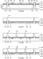
- a method of making the device 100 according to a first embodiment is described below in connection with the figures 5 to 9 .
- the device 100 comprises a matrix of diodes 102 forming a matrix of pixels of the device 100.
- the diodes 102 correspond to photo-emitting diodes, here LEDs.
- the device 100 is made from a substrate 128 comprising for example sapphire and/or silicon and/or a semiconductor for example similar to that used to form the active part of the diodes 102, and/or silicide carbon and/or glass and/or any other material allowing the substrate 128 to form a growth substrate allowing the production of the semiconductor stack forming the active part of the diodes 102 by epitaxy.
- the substrate 128 serves as a support for the deposition and/or growth of layers intended for the production of diodes 102 of device 100.
- the stack of layers from which the diodes 102 are going to be made is formed on the substrate 128.
- This stack comprises the first semiconductor layer 106, the emissive layer(s) 110, the second semiconductor layer 108 and a electrically conductive layer 130 forming, in each of the diodes 102, the portions 122 of the second electrodes (corresponding to the anode in the example described here) which will be in contact with the semiconductor of the second layer 108.
- the electrically conductive layer 130 is placed on the second layer 108.
- a first step forming the electrically conductive layer 130 is implemented in order to produce the portions 122 of the second electrodes of the diodes 102.
- This layer 130 is for example deposited on the layer 108 then removed locally by a so-called “lift-off” process in order to to form the portions 122 which will be, within the same region of the stack, surrounded by first trenches 112 and comprising one or more second trenches 118, electrically insulated from each other.
- the structure obtained at this stage of the process is represented on the figure 5 .
- the areas removed from the electrically conductive layer 130 are arranged substantially opposite the regions where the second trenches 118 will be made subsequently.
- a layer intended to form a dielectric hard mask is then placed on the electrically conductive layer 130.
- the material of this layer is for example SiO 2 or SIN.
- This layer is etched to form a hard dielectric mask 132 which will serve in particular as a mask for etching the other layers of the stack.
- the pattern of this hard mask 132 corresponds to that of the first trenches 112.
- etching through the layers 130, 108, 110 and a first part of the thickness of the first layer 106 is then implemented according to the pattern of the hard dielectric mask 132.
- This etching corresponds for example to a dry etching, for example by a Cl 2 -based plasma or an RIE etching, for example ICP-RIE (reactive ion etching by a plasma torch system, or “Inductively Coupled Plasma—Reactive Ion Etching”).
- This etching is stopped at a depth level located in the first layer 106 and such that the bottom walls of the etched trenches are formed by the first layer 106.
- the thickness of the first layer 106 etched during this etching is equal to l thickness e 1 .
- This etching is carried out such that the remaining thickness of the first layer 106, that is to say the second part of the thickness of the first layer 106 e 2 , is sufficient to make good electrical contact between the semiconductors of the first layer 106 and the first electrically conductive portions 116 which will be made later in the first trenches 112. This etching forms a first part of the first trenches 112.
- a dielectric layer corresponding for example to a SiN/Si0 2 bilayer or comprising Al 2 O 3 , and forming a passivation layer, is then deposited with a conforming thickness, for example comprised between around 5 nm and 1 ⁇ m and advantageously equal to approximately 200 nm, on the hard mask 132 and along the walls of the first parts of the first trenches 112, therefore covering the side walls formed of the hard mask 132 and of the regions of the stack of layers 106, 108, 110, 130 which are surrounded by the first parts of the first trenches 112 engraved.
- the dielectric layer is also deposited on the non-etched parts of the first layer 106 forming the bottom walls of these first parts of the first trenches 112.
- This dielectric layer is for example formed by a deposit of the PECVD type (chemical vapor deposition assisted by plasma) or ALD (atomic layer deposition) depending on the nature of the material(s) deposited.
- Anisotropic etching for example dry etching such as RIE etching, is then implemented such that the parts of the dielectric layer located in the first parts of the first trenches 112 and not covering the side walls of the first parts of the first trenches 112 are removed, thus revealing the parts of the first layer 106 lying at the bottom of the first parts of the first trenches 112.
- the parts of this dielectric layer covering the upper face of the hard mask 132 are also removed. Thus, only the portions 114 of the dielectric layer covering the side walls of the first parts of the first trenches 112 are retained.
- a second etching of the stack is implemented, extending the first trenches 112 through the remaining thickness e 2 of the first layer 106 of semiconductor until reaching the substrate 128, that is to say until 'so that the bottom walls of the first trenches 112 are formed by the substrate 128. form electrical contact areas for the first electrically conductive portions 116.
- Openings are then made through dielectric mask 132, forming locations for making electrical connection elements 124 intended to ensure electrical contacts with the second electrodes. These openings pass through the entire thickness of the dielectric mask 132 so that the bottom walls of these openings are formed by the electrically conductive portions 122. This etching is for example of the ICP-RIE type.
- One or more electrically conductive materials are then deposited in the first trenches 112 and in the locations of the electrical connections 124, forming the first electrically conductive portions 116 and the electrical connection elements 124.
- a first electrically conductive material can be deposited in the first trenches 112 and in the locations of the electrical connection elements 124 as well as on the dielectric mask 132.
- This first electrically conductive material is deposited conformally, it that is to say, by forming a layer of substantially constant thickness on the dielectric mask 132 and along the side walls and the bottom walls of the first trenches 112 and of the locations of the electrical connection elements 124.
- this first material electrically conductive can be formed by the deposition, for example of the PVD type, of a first layer of titanium with a thickness for example of less than approximately 300 nm, followed by a deposition, for example PVD, of a second layer of aluminum with a thickness for example between about 50 nm and 1 ⁇ m.
- the deposition techniques implemented are chosen so that they are adapted to the significant form factor of the volumes formed by the first trenches 112, and correspond for example to those implemented to deposit the electrically conductive material(s) of the conductive vias or TSV (“Through-Silicon Via”).
- a second electrically conductive material can be deposited by filling the remaining volumes of the first trenches 112 and of the locations of the electrical connection elements 124.
- the thickness of this second electrically conductive material can be such that it also covers the parts of the first electrically conductive material arranged on the dielectric mask 132.
- This second electrically conductive material is for example copper which can be formed by the implementation of a full plate electrochemical deposition (ECD or "Electro-Chemical Deposition"), it is that is to say on the whole of the structure previously carried out.
- a chemical-mechanical planarization (CMP) can then be implemented in order to remove the portions of the first and second electrically conductive materials which protrude from the first trenches 112 and from the locations of the electrical connection elements 124. This planarization makes it possible to complete the production electrically conductive portions 116 and electrical connections 124 and to electrically insulate these electrically conductive portions 116 vis-à-vis the electrical connections 124.
- the structure obtained at this stage of the process corresponds to that visible on the figure 6 .
- device 100 includes other regions of the stack also surrounded by first trenches 112 and which are not visible in these figures.
- the first electrically conductive portions 116 are electrically well insulated from the layers 108 and 110.
- the thickness of the dielectric portions 114 can be chosen such that an acceptable leakage current is tolerated on each of the diodes 102, by example less than approximately 1% of the nominal current passing through diode 102, when they are subjected to a potential difference (applied between the cathode and the anode) for example of the order of 4 volts.
- the minimum thickness of the dielectric portions 114 is for example comprised between approximately 3 nm and 5 nm, or between 3 nm and 4 nm, depending on the material or materials used to produce the dielectric portions 114.
- the structure produced is then hybridized on the support 104.
- this hybridization can correspond to a direct bonding (“direct bonding”, also called bonding by molecular adhesion), or a copper-oxide hybrid bonding and Au/Au thermocompression, or make use of electrical connection elements between the matrix of diodes 102 (and more specifically the electrical connection elements 124) and the electronic circuit such as, for example, fusible alloy balls (comprising for example SnAg and/or indium ), or to copper pillars covered with solder material, or to micro-inserts, or to micro-tubes.
- direct bonding also called bonding by molecular adhesion
- copper-oxide hybrid bonding and Au/Au thermocompression or make use of electrical connection elements between the matrix of diodes 102 (and more specifically the electrical connection elements 124) and the electronic circuit such as, for example, fusible alloy balls (comprising for example SnAg and/or indium ), or to copper pillars covered with solder material,
- the substrate 128 is removed, thus freeing the rear faces of the diodes through which the light is intended to enter or leave depending on whether the diodes 102 are photo-emitting or photo-receiving diodes (see figure 7 ).
- the substrate 128 is for example removed by laser lifting ("laser lift-off" in English) when the substrate 128 comprises sapphire, or by grinding (“grinding" in English) and selective chemical attack when the substrate 128 comprises for example a semiconductor such as silicon.
- the second trenches 118 are then made through part of the thickness of the first layer 106, such that the bottom walls of these second trenches 118 are formed by the material of the first layer 106 (see figure 8 ).
- the second trenches 118 are for example produced by implementing etching carried out using a hard mask, for example of SiO 2 . These second trenches 118 mark the physical and optical separation between the diodes 102 produced in the region of the stack surrounded by the first trenches 112.
- the second trenches 118 When the second trenches 118 are intended to be filled with at least one electrically conductive material performing a electrical contact with the semiconductor of the first layer 106, the second trenches 118 have at least an overlap region with the first trenches 112 to ensure continuity of electrical contact with the semiconductor of the first layer 106.
- the production of the device 100 is completed by the filling of the second trenches 118 with at least one electrically conductive material forming second electrically conductive portions 134 (see figure 9 ).
- This filling can be obtained by implementing steps similar to those implemented to produce the first electrically conductive portions 116.
- the hard mask used during the etching and filling of the second trenches 118 can be kept if it is transparent to the radiation, or suppressed, or even structured (for example by photonic crystals) to improve the light extraction or the directivity of emission.
- a transparent electrically conductive material for example ITO (indium and tin oxide) or AZO (zinc and aluminum oxide) or GZO ( zinc and gallium oxide), on the upper face of the assembly produced in order to improve the electrical contact between the semiconductor of the first layer 106 and the first and second electrically conductive portions 116, 134.
- a transparent electrically conductive material for example ITO (indium and tin oxide) or AZO (zinc and aluminum oxide) or GZO ( zinc and gallium oxide)
- the transfer of the diodes 102 onto the support 104 corresponds to a substrate-to-substrate, or “wafer-to-wafer” connection, that is to say that several matrices of diodes 102 are produced simultaneously in the layers 106, 108, 110 and that these matrices are transferred together on a substrate forming the support 104.
- This configuration is schematized on the figure 10 , on which the reference 136 designates the connection interface (bonding, interconnection elements, etc.) between the diode matrices 102 and the substrate forming the support 104.
- the matrices of diodes 102 produced simultaneously in the layers 106, 108, 110 to be first of all cut out in the form of individual chips, then transferred individually onto the substrate forming the support 104.
- This variant corresponds to an attachment of chip-to-substrate type, or "chip-to-wafer", implemented with the hybridization techniques mentioned above.
- the spaces between the diode arrays 102 are filled with a material 138, for example a dielectric. This configuration is schematized on the figure 11 .
- the matrices of diodes 102 produced simultaneously in the layers 106, 108, 110 can be first of all cut out in the form of individual chips, then transferred individually onto the substrate forming the support 104 also previously cut out in the form of individual chips.
- This other variant corresponds to chip-to-chip or "chip-to-chip” type connection.
- Each assembly formed by a matrix of diodes 102 and a control circuit is then transferred to another support 140 and the spaces between the sets "chips of diode matrices 102 transferred to chips of support substrates 104" are filled with a material 138, for example a dielectric.
- This configuration is schematized on the figure 12 .
- a cutting step is implemented to separate the devices 100 from each other.
- the first trenches 112 are made by etching the entire thickness of the stack formed by the layers 106, 108 and 110.
- the second etching of the stacking implemented after having produced the dielectric portions 114 is not carried out through the entire remaining thickness of the first layer 106, but through only part of this remaining thickness.
- the first electrically conductive portions 116 produced in the first trenches 112 are in electrical contact with the material of the first layer 106 at the level of the parts of the side walls of the first trenches 112 which are not covered by the dielectric portions 114 and at the level of the bottom walls of the first trenches 112.
- the first layer 106 is formed from the face against which the substrate 128 was previously located, until reaching the first electrically conductive portions 116.
- This thinning makes it possible to reduce the optical crosstalk between the pixels and makes it possible to reduce the width of the first trenches 112 while maintaining a constant aspect ratio (lithography and deep etching constraint).
- the first trenches 112 are etched, before transfer onto the support 104, through the layers 130, 106, 108 and 110 with a depth equal to the desired height for the first electrically conductive portions 116.
- the first trenches 112 are etched, before the transfer onto the support 104, partially through the entire thickness of the layer 130, of the second layer 108 (and of the emissive layer(s) 110 if such layers are present in the stack) and through only part (thickness e 1 ) of the thickness of the first layer 106.
- the dielectric portions 114 and electrically conductive portions 136, forming first parts of the portions 116, are then made in those parts of the first trenches 112 which do not cross the entire thickness of the first layer 106 (see figure 13 ).
- the assembly is then transferred to the support 104, as in the first embodiment.
- An etching is then implemented to finish etching the first trenches 112 and at the same time etch the second trenches 118 (see figure 14 ).
- the first trenches 112 and the second trenches 118 are then filled with one or more electrically conductive materials, thus completing the production of the first electrically conductive portions 116 and forming the second electrically conductive portions 134 (see figure 15 ).
- the first electrically conductive portions 116 are therefore produced in two stages. This is advantageous because the remaining thickness (thickness e 2 ) of the first layer 106 which is not etched during the production of the first part of the portions 116 (step visible on the figure 13 ) corresponds to the depth of the second trenches 118. The first parts 136 of the portions 116 then form an etching stop material during the making of the second trenches 118 and the completion of the first trenches 112.
- this second production method it is also possible to thin the first layer 106 after the removal of the substrate 128 and before the etching of the second trenches 118. doped arranged on the side of the substrate 128, this thinning being able to eliminate this undoped part.
- This second embodiment also makes it possible to relax the constraints on the width of the first trenches 112. Indeed, given that the etching of these trenches requires the implementation of two distinct steps, on both sides of the stack, the depth of material to be etched at each of these two steps is therefore less than when the first trenches 112 are made with the implementation of a single etching step, which makes it possible to reduce the aspect ratio in English, i.e. the ratio of the value of the depth of a trench to the value of the width of the trench) of the trenches. This thinning therefore ultimately makes it possible to obtain first trenches 112 that are narrower than when they are made with the implementation of a single etching step through the entire thickness of the layers 130, 106, 108 and 110.
- the matrix of pixels produced comprises several regions of the stack each surrounded by first trenches, and second trenches are produced in at least part of these regions.
- the matrix of pixels of device 100 it is possible for the matrix of pixels of device 100 to comprise a single region of the stack surrounded by first trenches 112, and for this region to be crossed by second trenches 118 which therefore define the pitch of all the pixels of this matrix.
- the figure 16 corresponds to a top view of such an embodiment.
- This other exemplary embodiment is very advantageous because in all the pixels of the matrix, there is no damage to the lateral flanks of the portions of the layers 108 and 110.
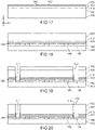
- a method of making the device 100 according to a third embodiment is described below in connection with the figures 17 to 22 .
- a stack similar to that previously described in connection with the figure 5 is made on the substrate 128.
- the etched spaces between the electrically conductive portions 122 are filled with a dielectric material 142 deposited and planarized with a stop on the portions 122 (see figure 17 ).
- first electrical contacts 144 are made on the support 104 and are intended to be connected to the electrically conductive portions 122.
- Second electrical contacts 146 are also made on the support 104 and are intended to be connected to the first electrically conductive portions 116.
- the first and second electrical contacts 144, 146 are connected to the electronic control circuit of the support 104 and are electrically insulated from each other by a dielectric material 148 deposited between these contacts (see figure 18 ).
- the substrate 128 is removed.
- the hard mask 132 is then produced on the stack, then the first trenches 112 are etched through the entire thickness of the layers 106, 108, 110, until reaching the first electrical contacts 146.
- the dielectric portions 114 are then made in the first trenches 112, against the side flanks of the layers 108, 110 and on the first part of the thickness e 1 of the first layer 106 (see figure 19 ).
- the dielectric portions 114 are for example made as described in the document FR 3 073 669 A1 .
- the first electrically conductive portions 116 are then made in the remaining volume of the first trenches 112, by implementing steps similar to those previously described for the first and second embodiments (see figure 20 ).
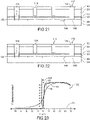
- the pattern of the second trenches 118 is then etched into the hard mask 132, then through part of the thickness of the first layer 106 ( figure 21 ).
- the device 100 is then completed by filling the second trenches 118 with at least one electrically conductive material forming the second electrically conductive portions 134 (see figure 22 ).
- the figure 23 represents simulations of illumination carried out in a pixel of GaN defined by second trenches similar to those carried out within the device 100. This simulation is obtained with a pixel formed in a stack of GaN of height equal to 7 ⁇ m, with these trenches which do not cross a part of the GaN with a thickness equal to 200 nm. The light emission occurs in the part of the thickness not crossed by the second trenches 118, which bears the reference 20 on the figure 23 .
- the width of the second trench 118 visible on the figure 23 is equal to 3 ⁇ m.
- curve 10 represents the relative illumination obtained in the absence of the second trench 118
- curve 12 represents the relative illumination obtained in the presence of the second trench 118 when the latter is not filled by a electrically conductive material and here filled with air
- the curve 14 represents the relative illumination obtained in the presence of the second trench 118 when the latter is filled with aluminum forming a second electrically conductive portion 134.
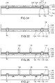
- a method of making the device 100 according to a fourth embodiment is described below in connection with the figures 24 to 27 .
- the first trenches 112 are etched, before the transfer onto the support 104, partially through the entire thickness of the layer 130, of the second layer 108 (and of the emissive layer(s) 110 if such layers are present in the stack) and through only part (thickness e 1 ) of the thickness of the first layer 106.
- the dielectric portions 114 and the first electrically conductive portions 116 are then made in the first trenches 112 which do not do not cross the entire thickness of the first layer 106 (see figure 24 ). At this stage of the process, the first electrically conductive portions 116 are completed and are in electrical contact with the material of the first layer 106 at the level of the bottom walls 150 of the first trenches 112.
- the assembly is then transferred to the support 104, as in the second embodiment (see figure 25 ).
- the second trenches 118 are then filled with one or more electrically conductive materials, forming the second electrically conductive portions 134 (see figure 27 ).
- the device 100 comprises a matrix of diodes 102 which are light-emitting diodes, the microelectronic device being able to form part of an LED display device (screens, projector, wall of pictures, etc.).
- This matrix of diodes 102 comprises the first electrically conductive portions 116 which form a cathode common to all the diodes 102, and each diode 102 comprises a second electrically conductive portion 122 forming an anode allowing individual addressing of each of the diodes 102.
- the microelectronic device 100 can comprise a matrix of diodes 102 which are photo-receiving diodes, or photodiodes.
- the anodes and the cathodes of the diodes 102 are not used to supply current to the diodes 102 but to recover the currents photo-generated by the diodes 102.
- the diodes 102 may not include layers 110 of intrinsic semiconductor between the first and second layers 106, 108. In this case, the p and n doped semiconductors are then placed directly against each other.
- optical elements on the diodes 102, for example phosphors modifying the wavelength emitted by the diodes 102.
Landscapes
- Led Devices (AREA)
- Engineering & Computer Science (AREA)
- Manufacturing & Machinery (AREA)
- Element Separation (AREA)
- Light Receiving Elements (AREA)
Claims (15)
- Vorrichtung (100) mit einer Matrix aus lichtemittierenden und/oder lichtempfangenden Dioden (102), die mindestens umfasst:- einen Stapel aus mindestens einer ersten (106) und einer zweiten (108) Schicht aus Halbleitern, die gemäß unterschiedlichen Leitfähigkeitstypen dotiert sind, wobei jede der Dioden (102) einen Abschnitt der ersten Schicht (106) umfasst, der einem Abschnitt der zweiten Schicht (108) überlagert ist;- erste Gräben (112), die durch die gesamte Dicke der zweiten Schicht (108) und mindestens einen Teil der Dicke der ersten Schicht (106) hindurchgehen und mindestens eine Region des Stapels, in der mehrere Dioden (102) gebildet sind, umgeben;- dielektrische Abschnitte (114), die in den ersten Gräben (112) angeordnet sind und Seitenflanken der Region des Stapels über die gesamte Dicke der zweiten Schicht (108) und einen ersten Teil der Dicke der ersten Schicht (106) bedecken;- erste elektrisch leitende Abschnitte (116), die in den ersten Gräben (112) angeordnet sind, die Seitenflanken der Region des Stapels über einen zweiten Teil der Dicke der ersten Schicht (106), der nicht von den dielektrischen Abschnitten (114) bedeckt ist, bedecken und/oder Bodenwände (150) der ersten Gräben (112) bedecken, und mindestens einen Teil von ersten Elektroden der Dioden (102), die in der Region des Stapels gebildet sind, bilden;- mindestens einen zweiten Graben (118), der von einer ersten Seite (120) der ersten Schicht (106), die einer der zweiten Schicht (108) zugewandten zweiten Seite der ersten Schicht (106) gegenüberliegt, teilweise durch die Dicke der ersten Schicht (106) hindurchgeht und die Abschnitte der ersten Schicht (106) der in der Region des Stapels gebildeten Dioden (102) trennt, ohne durch die Grenzfläche zwischen der ersten und der zweiten Schicht (106, 108) hindurchzugehen;- mehrere zweite Elektroden (122, 124), die elektrisch voneinander isoliert sind und jeweils elektrisch mit einem der Abschnitte der zweiten Schicht (108) der in der Region des Stapels gebildeten Dioden (102) verbunden sind;und wobei die Abschnitte der zweiten Schicht (108) der in der Region des Stapels gebildeten Dioden (102) einen durchgängigen Halbleiterabschnitt bilden, durch den die ersten und der zweite Graben (112, 118) nicht hindurchgehen.
- Vorrichtung (100) nach Anspruch 1, die weiter mindestens einen zweiten elektrisch leitenden Abschnitt (134) umfasst, der im zweiten Graben (118) angeordnet ist.
- Vorrichtung (100) nach Anspruch 2, wobei der zweite elektrisch leitende Abschnitt (134) elektrisch mit den ersten elektrisch leitenden Abschnitten (116) gekoppelt ist und zusammen mit den ersten elektrisch leitenden Abschnitten (116) die ersten Elektroden der Dioden (102) bildet.
- Vorrichtung (100) nach Anspruch 3, wobei:- alle Dioden (102) der Matrix in der Region des Stapels gebildet sind, und- jede der Dioden (102) der Matrix durch mindestens einen der zweiten Gräben (118) von einer oder mehreren benachbarten Dioden (102) getrennt ist.
- Vorrichtung (100) nach einem der Ansprüche 1 bis 3, wobei:- die ersten Gräben (112) mehrere Regionen des Stapels, in denen die Dioden (102) der Matrix gebildet sind, umgeben, und- eine oder mehrere dieser Regionen jeweils den zweiten Graben (118) oder mehrere zweite Gräben (118) umfassen.
- Vorrichtung (100) nach Anspruch 5, wobei die Region(en) des Stapels, die den oder die zweiten Gräben (118) umfasst bzw. umfassen, einen zentralen Teil der Dioden- (102) Matrix bilden.
- Vorrichtung (100) nach einem der vorstehenden Ansprüche, die weiter eine elektronische Steuerschaltung umfasst, auf der der Stapel der ersten und der zweiten Schicht (106, 108) angeordnet ist und mit der die ersten und die zweiten Elektroden der Dioden (102) elektrisch gekoppelt sind.
- Vorrichtung (100) nach einem der vorstehenden Ansprüche, wobei:- die Dioden (102) Photodioden entsprechen, wobei der Stapel weiter mindestens eine intrinsische Halbleiterschicht (110) umfasst, die zwischen der ersten und der zweiten Schicht (106, 108) und so angeordnet ist, dass Seitenflanken der intrinsischen Halbleiterschicht (110), die in den ersten Gräben (112) vorliegen, von den dielektrischen Abschnitten (114) bedeckt sind, wobei die zweiten Gräben (118) nicht durch die intrinsische Halbleiterschicht (110) hindurchgehen, oder- die Dioden (102) Leuchtdioden, LED, entsprechen, wobei der Stapel mindestens eine emittierende Quantentopfschicht (110) umfasst, die zwischen der ersten und der zweiten Schicht (106, 108) und so angeordnet ist, dass Seitenflanken der emittierenden Schicht (110), die in den ersten Gräben (112) vorliegen, von den dielektrischen Abschnitten (114) bedeckt sind, wobei die zweiten Gräben (118) nicht durch die emittierende Schicht (110) hindurchgehen.
- Verfahren zur Herstellung einer Vorrichtung (100) mit einer Matrix aus lichtemittierenden und/oder lichtempfangenden Dioden (102), das mindestens die folgenden Schritte umfasst:- Herstellen eines Stapels aus mindestens einer ersten und einer zweiten Schicht (106, 108) aus Halbleitern, die gemäß unterschiedlichen Leitfähigkeitstypen dotiert sind, wobei jede der Dioden (102) einen Abschnitt der ersten Schicht (106) enthalten soll, der einem Abschnitt der zweiten Schicht (108) überlagert ist;- Herstellen von mehreren zweiten Elektroden (122, 124), die elektrisch voneinander isoliert sind und jeweils elektrisch mit einem der Abschnitte der zweiten Schicht (108) der Dioden (102), die in der Region des Stapels gebildet werden sollen, verbunden sind;- Herstellen von ersten Gräben (112), die durch die gesamte Dicke der zweiten Schicht (108) und mindestens einen Teil der Dicke der ersten Schicht (106) hindurchgehen und mindestens eine Region des Stapels, in der mehrere Dioden (102) gebildet werden sollen, umgeben;- Herstellen von dielektrischen Abschnitten (114), die in den ersten Gräben (112) angeordnet sind und Seitenflanken der Region des Stapels über die gesamte Dicke der zweiten Schicht (108) und einen ersten Teil der Dicke der ersten Schicht (106) bedecken;- Herstellen von ersten elektrisch leitenden Abschnitten (116), die in den ersten Gräben (112) angeordnet sind, die Seitenflanken der Region des Stapels über einen zweiten Teil der Dicke der ersten Schicht (106), der nicht von den dielektrischen Abschnitten (114) bedeckt ist, bedecken und/oder Bodenwände (150) der ersten Gräben (112) bedecken, und mindestens einen Teil von ersten Elektroden der Dioden (102), die in der Region des Stapels gebildet werden sollen, bilden;- Herstellen von mindestens einem zweiten Graben (118), der von einer ersten Seite (120) der ersten Schicht (106), die einer der zweiten Schicht (108) zugewandten zweiten Seite der ersten Schicht (106) gegenüberliegt, teilweise durch die Dicke der ersten Schicht (106) hindurchgeht und die Abschnitte der ersten Schicht (106) der in der Region des Stapels gebildeten Dioden (102) trennt, ohne durch die Grenzfläche zwischen der ersten und der zweiten Schicht (106, 108) hindurchzugehen;und wobei die Abschnitte der zweiten Schicht (108) der in der Region des Stapels gebildeten Dioden (102) einen durchgängigen Halbleiterabschnitt bilden, durch den die ersten und der zweite Graben (112, 118) nicht hindurchgehen.
- Verfahren nach Anspruch 9, wobei der Stapel durch Epitaxie auf einem Substrat (128) so hergestellt wird, dass die erste Schicht (106) zwischen dem Substrat (128) und der zweiten Schicht (108) angeordnet ist.
- Verfahren nach Anspruch 10, wobei die ersten Gräben (112), die dielektrischen Abschnitte (114) und die ersten elektrisch leitenden Abschnitte (116) hergestellt werden, indem die folgenden Schritte umgesetzt werden:- nach dem Herstellen der zweiten Elektroden, erstes Ätzen des Stapels durch die zweite Schicht (108) und den ersten Teil der Dicke der ersten Schicht (106) hindurch gemäß einem die ersten Gräben (112) definierenden Muster, wodurch erste Teile der ersten Gräben (112) gebildet werden, und anschließend- Herstellen der dielektrischen Abschnitte (114), die die Seitenflanken der ersten Teile der ersten Gräben (112) bedecken, und anschließend- zweites Ätzen des Stapels durch mindestens einen Teil einer verbleibenden Dicke der ersten Schicht (106) hindurch und gemäß dem die ersten Gräben (112) definierenden Muster, wodurch die Herstellung der ersten Gräben (112) vollendet wird, und anschließend- Abscheiden mindestens eines elektrisch leitenden Materials in den ersten Gräben (112), wodurch die ersten elektrisch leitenden Abschnitte (116) gebildet werden.
- Verfahren nach einem der Ansprüche 10 und 11, das nach dem Herstellen der ersten elektrisch leitenden Abschnitte (116) und vor dem Herstellen des zweiten Grabens (118) weiter das Umsetzen der folgenden Schritte umfasst:- Befestigen des Stapels an einem Träger (104) so, dass der Stapel zwischen dem Substrat (128) und dem Träger (104) angeordnet ist, und anschließend- Entfernen des Substrats (128).
- Verfahren nach Anspruch 10, wobei die ersten Gräben (112), die dielektrischen Abschnitte (114), die ersten elektrisch leitenden Abschnitte (116) und der zweite Graben (118) hergestellt werden, indem die folgenden Schritte umgesetzt werden:- nach dem Herstellen der zweiten Elektroden, erstes Ätzen des Stapels durch die zweite Schicht (108) und einen Teil der Dicke der ersten Schicht (106) hindurch gemäß einem die ersten Gräben (112) definierenden Muster, wodurch erste Teile der ersten Gräben (112) gebildet werden, und anschließend- Herstellen der dielektrischen Abschnitte (114), die die Seitenflanken der ersten Teile der ersten Gräben (112) bedecken, und anschließend- Abscheiden mindestens eines elektrisch leitenden Materials in den ersten Teilen der ersten Gräben (112), wodurch erste Teile der ersten elektrisch leitenden Abschnitte (116) gebildet werden, und anschließend- Befestigen des Stapels an einem Träger (104) so, dass der Stapel zwischen dem Substrat (128) und dem Träger (104) angeordnet ist, und anschließend- Entfernen des Substrats (128), wodurch die erste Seite (120) der ersten Schicht (106) freigelegt wird, und anschließend- zweites Ätzen des Stapels durch die erste Seite (120) der ersten Schicht (106) hindurch und gemäß einem die ersten und die zweiten Gräben (112, 118) definierenden Muster, mit Stopp an den ersten Teilen der ersten elektrisch leitenden Abschnitte (116), wodurch zweite Teile der ersten Gräben (112) und der zweite Graben (118) gebildet werden, und anschließend- Abscheiden des elektrisch leitenden Materials in den zweiten Teilen der ersten Gräben (112) und im zweiten Graben (118), wodurch die Herstellung der ersten elektrisch leitenden Abschnitte (116) und mindestens eines im zweiten Graben (118) angeordneten zweiten elektrisch leitenden Abschnitts (134) vollendet wird.
- Verfahren nach Anspruch 10, wobei die ersten Gräben (112), die dielektrischen Abschnitte (114), die ersten elektrisch leitenden Abschnitte (116) und der zweite Graben (118) hergestellt werden, indem die folgenden Schritte umgesetzt werden:- nach dem Herstellen der zweiten Elektroden, Befestigen des Stapels an einem Träger (104) so, dass der Stapel zwischen dem Substrat (128) und dem Träger (104) angeordnet ist, und anschließend- Entfernen des Substrats (128), wodurch die erste Seite (120) der ersten Schicht (106) freigelegt wird, und anschließend- erstes Ätzen des Stapels durch die erste und die zweite Schicht (106, 108) hindurch gemäß einem die ersten Gräben (112) definierenden Muster, wodurch die ersten Gräben (112) gebildet werden, und anschließend- Herstellen der dielektrischen Abschnitte (114), die die Seitenflanken der ersten Teile der ersten Gräben (112) bedecken, und anschließend- Abscheiden mindestens eines elektrisch leitenden Materials in den ersten Gräben (112), wodurch die ersten elektrisch leitenden Abschnitte (116) gebildet werden, und anschließend- zweites Ätzen des Stapels durch einen Teil der Dicke der ersten Schicht (106) hindurch und gemäß einem den zweiten Graben (118) definierenden Muster, wodurch der zweite Graben (118) gebildet wird.
- Verfahren nach Anspruch 10, wobei die ersten Gräben (112), die dielektrischen Abschnitte (114), die ersten elektrisch leitenden Abschnitte (116) und der zweite Graben (118) hergestellt werden, indem die folgenden Schritte umgesetzt werden:- nach dem Herstellen der zweiten Elektroden, erstes Ätzen des Stapels durch die zweite Schicht (108) und den ersten Teil der Dicke der ersten Schicht (106) hindurch gemäß einem die ersten Gräben (112) definierenden Muster, wodurch die ersten Gräben (112) gebildet werden, und anschließend- Herstellen der dielektrischen Abschnitte (114), die die Seitenflanken der ersten Gräben (112) bedecken, und anschließend- Abscheiden mindestens eines elektrisch leitenden Materials in den ersten Gräben (112), wodurch die ersten elektrisch leitenden Abschnitte (116) gebildet werden, die die Bodenwände (150) der ersten Gräben (112) bedecken, und anschließend- Befestigen des Stapels an einem Träger (104) so, dass der Stapel zwischen dem Substrat (128) und dem Träger (104) angeordnet ist, und anschließend- Entfernen des Substrats (128), sodass die erste Seite (120) der ersten Schicht (106) freigelegt wird, und anschließend- zweites Ätzen des Stapels durch die erste Seite (120) der ersten Schicht (106) hindurch und gemäß einem den zweiten Graben (118) definierenden Muster, wodurch der zweite Graben (118) gebildet wird.
Applications Claiming Priority (1)
| Application Number | Priority Date | Filing Date | Title |
|---|---|---|---|
| FR2003427A FR3109018A1 (fr) | 2020-04-06 | 2020-04-06 | Dispositif a matrice de diodes photo-emettrices et/ou photo-receptrices |
Publications (2)
| Publication Number | Publication Date |
|---|---|
| EP3893281A1 EP3893281A1 (de) | 2021-10-13 |
| EP3893281B1 true EP3893281B1 (de) | 2022-08-10 |
Family
ID=70918657
Family Applications (1)
| Application Number | Title | Priority Date | Filing Date |
|---|---|---|---|
| EP21166778.7A Active EP3893281B1 (de) | 2020-04-06 | 2021-04-01 | Lichtemittierende und/oder lichtempfangende diodenarray-vorrichtung |
Country Status (4)
| Country | Link |
|---|---|
| US (1) | US11581464B2 (de) |
| EP (1) | EP3893281B1 (de) |
| CN (1) | CN113497161B (de) |
| FR (1) | FR3109018A1 (de) |
Families Citing this family (12)
| Publication number | Priority date | Publication date | Assignee | Title |
|---|---|---|---|---|
| CN114766065B (zh) | 2019-06-19 | 2025-06-24 | 上海显耀显示科技有限公司 | 用于多色led像素单元的系统和方法 |
| US11942507B2 (en) * | 2020-03-11 | 2024-03-26 | Lumileds Llc | Light emitting diode devices |
| KR20230022942A (ko) * | 2020-06-03 | 2023-02-16 | 제이드 버드 디스플레이(상하이) 리미티드 | 수직 광 방출을 갖는 다색 led 픽셀 유닛을 위한 시스템들 및 방법들 |
| CN115843393A (zh) | 2020-06-03 | 2023-03-24 | 上海显耀显示科技有限公司 | 用于具有水平发光的多色led像素单元的系统和方法 |
| KR20230053438A (ko) * | 2021-10-14 | 2023-04-21 | 쓰리엠 이노베이티브 프로퍼티즈 캄파니 | 통합 전자 스택 |
| US12191285B2 (en) * | 2021-11-10 | 2025-01-07 | Infineon Technologies Ag | Optical projection device having a grid structure |
| TWI819497B (zh) * | 2022-02-17 | 2023-10-21 | 錼創顯示科技股份有限公司 | 微型發光二極體與微型發光二極體顯示面板 |
| JP7790282B2 (ja) * | 2022-06-24 | 2025-12-23 | 沖電気工業株式会社 | 半導体装置及び半導体装置製造方法 |
| WO2024025753A1 (en) * | 2022-07-25 | 2024-02-01 | Lumileds Llc | Light emitting diode devices with extended junction spacers |
| EP4634990A1 (de) * | 2022-12-12 | 2025-10-22 | Lumileds LLC | Strukturierte pixel von mikro-leuchtdioden (uleds) und chips |
| WO2025081416A1 (en) * | 2023-10-19 | 2025-04-24 | Jade Bird Display (shanghai) Limited | A micro led display panel |
| CN118248820A (zh) * | 2024-05-30 | 2024-06-25 | 晶能光电股份有限公司 | 一种Micro LED发光阵列及其制备方法 |
Family Cites Families (16)
| Publication number | Priority date | Publication date | Assignee | Title |
|---|---|---|---|---|
| JP2003249675A (ja) * | 2002-02-26 | 2003-09-05 | Sumitomo Electric Ind Ltd | 受光素子アレイ |
| KR102286109B1 (ko) * | 2014-08-05 | 2021-08-04 | 삼성전자주식회사 | 이미지 픽셀, 이를 포함하는 이미지 센서, 및 이를 포함하는 이미지 처리 시스템 |
| WO2016060676A1 (en) * | 2014-10-17 | 2016-04-21 | Intel Corporation | Microled display & assembly |
| FR3042913B1 (fr) | 2015-10-22 | 2019-07-12 | Commissariat A L'energie Atomique Et Aux Energies Alternatives | Diode micro-electronique a surface active optimisee |
| US10700114B2 (en) * | 2016-04-25 | 2020-06-30 | Sony Corporation | Solid-state imaging element, method for manufacturing the same, and electronic apparatus |
| US10204950B1 (en) * | 2017-09-29 | 2019-02-12 | Taiwan Semiconductor Manufacturing Company Ltd. | SPAD image sensor and associated fabricating method |
| FR3073669B1 (fr) | 2017-11-10 | 2021-11-05 | Commissariat Energie Atomique | Procede de fabrication d'un dispositif optoelectronique comprenant une pluralite de diodes |
| US10627673B2 (en) * | 2018-04-06 | 2020-04-21 | Glo Ab | Light emitting diode array containing a multilayer bus electrode and method of making the same |
| JP7105612B2 (ja) * | 2018-05-21 | 2022-07-25 | シャープ株式会社 | 画像表示素子およびその形成方法 |
| FR3086100B1 (fr) * | 2018-09-13 | 2022-08-12 | Commissariat Energie Atomique | Procede de fabrication d'un dispositif optoelectronique comprenant une pluralite de diodes |
| FR3089746A1 (fr) * | 2018-12-06 | 2020-06-12 | Commissariat A L'energie Atomique Et Aux Energies Alternatives | Procede d’adaptation de l’extraction lumineuse d’une diode electroluminescente |
| FR3095550B1 (fr) * | 2019-04-26 | 2021-05-21 | Commissariat Energie Atomique | Procede de realisation d’un dispositif photo-emetteur et/ou photo-recepteur a grille de separation optique metallique |
| CN110729322B (zh) * | 2019-10-22 | 2022-04-19 | 厦门乾照光电股份有限公司 | 一种垂直型led芯片结构及其制作方法 |
| FR3102613A1 (fr) * | 2019-10-28 | 2021-04-30 | Commissariat A L'energie Atomique Et Aux Energies Alternatives | Procede de realisation d’une diode photo-emettrice ou photo-receptrice |
| FR3104809B1 (fr) * | 2019-12-11 | 2021-12-17 | Commissariat Energie Atomique | Procede de realisation d’une couche de materiau structuree |
| FR3107105B1 (fr) * | 2020-02-10 | 2022-07-08 | Commissariat Energie Atomique | Dispositif d’éclairage directionnel |
-
2020
- 2020-04-06 FR FR2003427A patent/FR3109018A1/fr not_active Withdrawn
-
2021
- 2021-04-01 EP EP21166778.7A patent/EP3893281B1/de active Active
- 2021-04-02 US US17/221,344 patent/US11581464B2/en active Active
- 2021-04-06 CN CN202110368589.0A patent/CN113497161B/zh active Active
Also Published As
| Publication number | Publication date |
|---|---|
| US11581464B2 (en) | 2023-02-14 |
| CN113497161B (zh) | 2026-03-20 |
| CN113497161A (zh) | 2021-10-12 |
| FR3109018A1 (fr) | 2021-10-08 |
| US20210313499A1 (en) | 2021-10-07 |
| EP3893281A1 (de) | 2021-10-13 |
Similar Documents
| Publication | Publication Date | Title |
|---|---|---|
| EP3893281B1 (de) | Lichtemittierende und/oder lichtempfangende diodenarray-vorrichtung | |
| EP3667728B1 (de) | Verfahren zur herstellung einer vorrichtung mit lichtemittierenden und/oder lichtempfangenden dioden und mit einem selbst ausgerichteten kollimationsgitter | |
| EP3365924B1 (de) | Mikroelektronische diode mit optimierter aktiver oberfläche | |
| EP3817054B1 (de) | Verfahren zur herstellung mindestens einer lichtemittierenden oder lichtempfangenden diode | |
| EP3782193B1 (de) | Herstellungsverfahren einer optoelektronischen vorrichtung mit diodenmatrix | |
| EP3913680B1 (de) | Verfahren zur herstellung einer optoelektronischen vorrichtung, die eine vielzahl von dioden aus galliumnitrid umfasst | |
| EP3529834B1 (de) | Anzeigevorrichtung und verfahren zur herstellung solch einer vorrichtung | |
| EP3624192A1 (de) | Herstellungsverfahren einer optoelektronischen vorrichtung, die eine vielzahl von dioden umfasst | |
| EP4092746A1 (de) | Verfahren zur herstellung einer optoelektronischen vorrichtung | |
| FR2965105A1 (fr) | Detecteur bispectral multicouche a photodiodes | |
| EP3109900A1 (de) | Herstellungsverfahren einer vielzahl von dipolen in form von inseln, die selbstausrichtende elektroden umfassen | |
| EP4145507B1 (de) | Verfahren zur herstellung einer optoelektronischen vorrichtung und optoelektronische vorrichtung | |
| EP4631103A1 (de) | Verfahren zur herstellung einer optoelektronischen vorrichtung mit einer led und einer photodiode | |
| WO2024003085A1 (fr) | Dispositif optoélectronique et procédé de fabrication | |
| WO2021094177A1 (fr) | Procédé de fabrication d'un ensemble d'émetteurs de lumière | |
| EP4383338B1 (de) | Verfahren zur herstellung einer optoelektronischen vorrichtung mit einer led und einer photodiode | |
| EP4565039A1 (de) | Optoelektronische vorrichtung mit drei-elektroden-dioden und verfahren zu deren herstellung | |
| EP4167282A1 (de) | Verfahren zur herstellung einer optoelektronischen vorrichtung | |
| FR3157672A1 (fr) | Dispositif optoélectronique à diaphonie optique réduite |
Legal Events
| Date | Code | Title | Description |
|---|---|---|---|
| PUAI | Public reference made under article 153(3) epc to a published international application that has entered the european phase |
Free format text: ORIGINAL CODE: 0009012 |
|
| STAA | Information on the status of an ep patent application or granted ep patent |
Free format text: STATUS: REQUEST FOR EXAMINATION WAS MADE |
|
| 17P | Request for examination filed |
Effective date: 20210401 |
|
| AK | Designated contracting states |
Kind code of ref document: A1 Designated state(s): AL AT BE BG CH CY CZ DE DK EE ES FI FR GB GR HR HU IE IS IT LI LT LU LV MC MK MT NL NO PL PT RO RS SE SI SK SM TR |
|
| GRAP | Despatch of communication of intention to grant a patent |
Free format text: ORIGINAL CODE: EPIDOSNIGR1 |
|
| STAA | Information on the status of an ep patent application or granted ep patent |
Free format text: STATUS: GRANT OF PATENT IS INTENDED |
|
| INTG | Intention to grant announced |
Effective date: 20220321 |
|
| GRAS | Grant fee paid |
Free format text: ORIGINAL CODE: EPIDOSNIGR3 |
|
| GRAA | (expected) grant |
Free format text: ORIGINAL CODE: 0009210 |
|
| STAA | Information on the status of an ep patent application or granted ep patent |
Free format text: STATUS: THE PATENT HAS BEEN GRANTED |
|
| AK | Designated contracting states |
Kind code of ref document: B1 Designated state(s): AL AT BE BG CH CY CZ DE DK EE ES FI FR GB GR HR HU IE IS IT LI LT LU LV MC MK MT NL NO PL PT RO RS SE SI SK SM TR |
|
| REG | Reference to a national code |
Ref country code: AT Ref legal event code: REF Ref document number: 1511186 Country of ref document: AT Kind code of ref document: T Effective date: 20220815 Ref country code: CH Ref legal event code: EP |
|
| REG | Reference to a national code |
Ref country code: IE Ref legal event code: FG4D Free format text: LANGUAGE OF EP DOCUMENT: FRENCH |
|
| REG | Reference to a national code |
Ref country code: DE Ref legal event code: R096 Ref document number: 602021000292 Country of ref document: DE |
|
| REG | Reference to a national code |
Ref country code: NL Ref legal event code: MP Effective date: 20220810 |
|
| REG | Reference to a national code |
Ref country code: LT Ref legal event code: MG9D |
|
| PG25 | Lapsed in a contracting state [announced via postgrant information from national office to epo] |
Ref country code: SE Free format text: LAPSE BECAUSE OF FAILURE TO SUBMIT A TRANSLATION OF THE DESCRIPTION OR TO PAY THE FEE WITHIN THE PRESCRIBED TIME-LIMIT Effective date: 20220810 Ref country code: RS Free format text: LAPSE BECAUSE OF FAILURE TO SUBMIT A TRANSLATION OF THE DESCRIPTION OR TO PAY THE FEE WITHIN THE PRESCRIBED TIME-LIMIT Effective date: 20220810 Ref country code: PT Free format text: LAPSE BECAUSE OF FAILURE TO SUBMIT A TRANSLATION OF THE DESCRIPTION OR TO PAY THE FEE WITHIN THE PRESCRIBED TIME-LIMIT Effective date: 20221212 Ref country code: NO Free format text: LAPSE BECAUSE OF FAILURE TO SUBMIT A TRANSLATION OF THE DESCRIPTION OR TO PAY THE FEE WITHIN THE PRESCRIBED TIME-LIMIT Effective date: 20221110 Ref country code: NL Free format text: LAPSE BECAUSE OF FAILURE TO SUBMIT A TRANSLATION OF THE DESCRIPTION OR TO PAY THE FEE WITHIN THE PRESCRIBED TIME-LIMIT Effective date: 20220810 Ref country code: LV Free format text: LAPSE BECAUSE OF FAILURE TO SUBMIT A TRANSLATION OF THE DESCRIPTION OR TO PAY THE FEE WITHIN THE PRESCRIBED TIME-LIMIT Effective date: 20220810 Ref country code: LT Free format text: LAPSE BECAUSE OF FAILURE TO SUBMIT A TRANSLATION OF THE DESCRIPTION OR TO PAY THE FEE WITHIN THE PRESCRIBED TIME-LIMIT Effective date: 20220810 Ref country code: FI Free format text: LAPSE BECAUSE OF FAILURE TO SUBMIT A TRANSLATION OF THE DESCRIPTION OR TO PAY THE FEE WITHIN THE PRESCRIBED TIME-LIMIT Effective date: 20220810 |
|
| REG | Reference to a national code |
Ref country code: AT Ref legal event code: MK05 Ref document number: 1511186 Country of ref document: AT Kind code of ref document: T Effective date: 20220810 |
|
| PG25 | Lapsed in a contracting state [announced via postgrant information from national office to epo] |
Ref country code: PL Free format text: LAPSE BECAUSE OF FAILURE TO SUBMIT A TRANSLATION OF THE DESCRIPTION OR TO PAY THE FEE WITHIN THE PRESCRIBED TIME-LIMIT Effective date: 20220810 Ref country code: IS Free format text: LAPSE BECAUSE OF FAILURE TO SUBMIT A TRANSLATION OF THE DESCRIPTION OR TO PAY THE FEE WITHIN THE PRESCRIBED TIME-LIMIT Effective date: 20221210 Ref country code: HR Free format text: LAPSE BECAUSE OF FAILURE TO SUBMIT A TRANSLATION OF THE DESCRIPTION OR TO PAY THE FEE WITHIN THE PRESCRIBED TIME-LIMIT Effective date: 20220810 Ref country code: GR Free format text: LAPSE BECAUSE OF FAILURE TO SUBMIT A TRANSLATION OF THE DESCRIPTION OR TO PAY THE FEE WITHIN THE PRESCRIBED TIME-LIMIT Effective date: 20221111 |
|
| PG25 | Lapsed in a contracting state [announced via postgrant information from national office to epo] |
Ref country code: SM Free format text: LAPSE BECAUSE OF FAILURE TO SUBMIT A TRANSLATION OF THE DESCRIPTION OR TO PAY THE FEE WITHIN THE PRESCRIBED TIME-LIMIT Effective date: 20220810 Ref country code: RO Free format text: LAPSE BECAUSE OF FAILURE TO SUBMIT A TRANSLATION OF THE DESCRIPTION OR TO PAY THE FEE WITHIN THE PRESCRIBED TIME-LIMIT Effective date: 20220810 Ref country code: ES Free format text: LAPSE BECAUSE OF FAILURE TO SUBMIT A TRANSLATION OF THE DESCRIPTION OR TO PAY THE FEE WITHIN THE PRESCRIBED TIME-LIMIT Effective date: 20220810 Ref country code: DK Free format text: LAPSE BECAUSE OF FAILURE TO SUBMIT A TRANSLATION OF THE DESCRIPTION OR TO PAY THE FEE WITHIN THE PRESCRIBED TIME-LIMIT Effective date: 20220810 Ref country code: CZ Free format text: LAPSE BECAUSE OF FAILURE TO SUBMIT A TRANSLATION OF THE DESCRIPTION OR TO PAY THE FEE WITHIN THE PRESCRIBED TIME-LIMIT Effective date: 20220810 Ref country code: AT Free format text: LAPSE BECAUSE OF FAILURE TO SUBMIT A TRANSLATION OF THE DESCRIPTION OR TO PAY THE FEE WITHIN THE PRESCRIBED TIME-LIMIT Effective date: 20220810 |
|
| REG | Reference to a national code |
Ref country code: DE Ref legal event code: R097 Ref document number: 602021000292 Country of ref document: DE |
|
| PG25 | Lapsed in a contracting state [announced via postgrant information from national office to epo] |
Ref country code: SK Free format text: LAPSE BECAUSE OF FAILURE TO SUBMIT A TRANSLATION OF THE DESCRIPTION OR TO PAY THE FEE WITHIN THE PRESCRIBED TIME-LIMIT Effective date: 20220810 Ref country code: EE Free format text: LAPSE BECAUSE OF FAILURE TO SUBMIT A TRANSLATION OF THE DESCRIPTION OR TO PAY THE FEE WITHIN THE PRESCRIBED TIME-LIMIT Effective date: 20220810 |
|
| PLBE | No opposition filed within time limit |
Free format text: ORIGINAL CODE: 0009261 |
|
| STAA | Information on the status of an ep patent application or granted ep patent |
Free format text: STATUS: NO OPPOSITION FILED WITHIN TIME LIMIT |
|
| PG25 | Lapsed in a contracting state [announced via postgrant information from national office to epo] |
Ref country code: AL Free format text: LAPSE BECAUSE OF FAILURE TO SUBMIT A TRANSLATION OF THE DESCRIPTION OR TO PAY THE FEE WITHIN THE PRESCRIBED TIME-LIMIT Effective date: 20220810 |
|
| 26N | No opposition filed |
Effective date: 20230511 |
|
| PG25 | Lapsed in a contracting state [announced via postgrant information from national office to epo] |
Ref country code: SI Free format text: LAPSE BECAUSE OF FAILURE TO SUBMIT A TRANSLATION OF THE DESCRIPTION OR TO PAY THE FEE WITHIN THE PRESCRIBED TIME-LIMIT Effective date: 20220810 |
|
| PG25 | Lapsed in a contracting state [announced via postgrant information from national office to epo] |
Ref country code: LU Free format text: LAPSE BECAUSE OF NON-PAYMENT OF DUE FEES Effective date: 20230401 |
|
| REG | Reference to a national code |
Ref country code: BE Ref legal event code: MM Effective date: 20230430 |
|
| PG25 | Lapsed in a contracting state [announced via postgrant information from national office to epo] |
Ref country code: MC Free format text: LAPSE BECAUSE OF FAILURE TO SUBMIT A TRANSLATION OF THE DESCRIPTION OR TO PAY THE FEE WITHIN THE PRESCRIBED TIME-LIMIT Effective date: 20220810 |
|
| PG25 | Lapsed in a contracting state [announced via postgrant information from national office to epo] |
Ref country code: MC Free format text: LAPSE BECAUSE OF FAILURE TO SUBMIT A TRANSLATION OF THE DESCRIPTION OR TO PAY THE FEE WITHIN THE PRESCRIBED TIME-LIMIT Effective date: 20220810 |
|
| REG | Reference to a national code |
Ref country code: IE Ref legal event code: MM4A |
|
| PG25 | Lapsed in a contracting state [announced via postgrant information from national office to epo] |
Ref country code: BE Free format text: LAPSE BECAUSE OF NON-PAYMENT OF DUE FEES Effective date: 20230430 |
|
| PG25 | Lapsed in a contracting state [announced via postgrant information from national office to epo] |
Ref country code: IE Free format text: LAPSE BECAUSE OF NON-PAYMENT OF DUE FEES Effective date: 20230401 |
|
| PG25 | Lapsed in a contracting state [announced via postgrant information from national office to epo] |
Ref country code: IE Free format text: LAPSE BECAUSE OF NON-PAYMENT OF DUE FEES Effective date: 20230401 |
|
| PG25 | Lapsed in a contracting state [announced via postgrant information from national office to epo] |
Ref country code: IT Free format text: LAPSE BECAUSE OF FAILURE TO SUBMIT A TRANSLATION OF THE DESCRIPTION OR TO PAY THE FEE WITHIN THE PRESCRIBED TIME-LIMIT Effective date: 20220810 |
|
| PG25 | Lapsed in a contracting state [announced via postgrant information from national office to epo] |
Ref country code: BG Free format text: LAPSE BECAUSE OF FAILURE TO SUBMIT A TRANSLATION OF THE DESCRIPTION OR TO PAY THE FEE WITHIN THE PRESCRIBED TIME-LIMIT Effective date: 20220810 |
|
| REG | Reference to a national code |
Ref country code: DE Ref legal event code: R079 Ref document number: 602021000292 Country of ref document: DE Free format text: PREVIOUS MAIN CLASS: H01L0027150000 Ipc: H10H0029140000 |
|
| PG25 | Lapsed in a contracting state [announced via postgrant information from national office to epo] |
Ref country code: BG Free format text: LAPSE BECAUSE OF FAILURE TO SUBMIT A TRANSLATION OF THE DESCRIPTION OR TO PAY THE FEE WITHIN THE PRESCRIBED TIME-LIMIT Effective date: 20220810 |
|
| REG | Reference to a national code |
Ref country code: CH Ref legal event code: PL |
|
| PG25 | Lapsed in a contracting state [announced via postgrant information from national office to epo] |
Ref country code: CH Free format text: LAPSE BECAUSE OF NON-PAYMENT OF DUE FEES Effective date: 20240430 |
|
| PGFP | Annual fee paid to national office [announced via postgrant information from national office to epo] |
Ref country code: DE Payment date: 20250417 Year of fee payment: 5 |
|
| PGFP | Annual fee paid to national office [announced via postgrant information from national office to epo] |
Ref country code: GB Payment date: 20250424 Year of fee payment: 5 |
|
| PGFP | Annual fee paid to national office [announced via postgrant information from national office to epo] |
Ref country code: FR Payment date: 20250422 Year of fee payment: 5 |
|
| PG25 | Lapsed in a contracting state [announced via postgrant information from national office to epo] |
Ref country code: CY Free format text: LAPSE BECAUSE OF FAILURE TO SUBMIT A TRANSLATION OF THE DESCRIPTION OR TO PAY THE FEE WITHIN THE PRESCRIBED TIME-LIMIT; INVALID AB INITIO Effective date: 20210401 |
|
| PG25 | Lapsed in a contracting state [announced via postgrant information from national office to epo] |
Ref country code: HU Free format text: LAPSE BECAUSE OF FAILURE TO SUBMIT A TRANSLATION OF THE DESCRIPTION OR TO PAY THE FEE WITHIN THE PRESCRIBED TIME-LIMIT; INVALID AB INITIO Effective date: 20210401 |
|
| PG25 | Lapsed in a contracting state [announced via postgrant information from national office to epo] |
Ref country code: TR Free format text: LAPSE BECAUSE OF FAILURE TO SUBMIT A TRANSLATION OF THE DESCRIPTION OR TO PAY THE FEE WITHIN THE PRESCRIBED TIME-LIMIT Effective date: 20220810 |