EP3712878A2 - Stufe und emissionssteuerungstreiber damit - Google Patents
Stufe und emissionssteuerungstreiber damit Download PDFInfo
- Publication number
- EP3712878A2 EP3712878A2 EP20163919.2A EP20163919A EP3712878A2 EP 3712878 A2 EP3712878 A2 EP 3712878A2 EP 20163919 A EP20163919 A EP 20163919A EP 3712878 A2 EP3712878 A2 EP 3712878A2
- Authority
- EP
- European Patent Office
- Prior art keywords
- node
- transistor
- voltage
- coupled
- input terminal
- Prior art date
- Legal status (The legal status is an assumption and is not a legal conclusion. Google has not performed a legal analysis and makes no representation as to the accuracy of the status listed.)
- Granted
Links
Images


Classifications
-
- G—PHYSICS
- G09—EDUCATION; CRYPTOGRAPHY; DISPLAY; ADVERTISING; SEALS
- G09G—ARRANGEMENTS OR CIRCUITS FOR CONTROL OF INDICATING DEVICES USING STATIC MEANS TO PRESENT VARIABLE INFORMATION
- G09G3/00—Control arrangements or circuits, of interest only in connection with visual indicators other than cathode-ray tubes
- G09G3/20—Control arrangements or circuits, of interest only in connection with visual indicators other than cathode-ray tubes for presentation of an assembly of a number of characters, e.g. a page, by composing the assembly by combination of individual elements arranged in a matrix no fixed position being assigned to or needed to be assigned to the individual characters or partial characters
- G09G3/22—Control arrangements or circuits, of interest only in connection with visual indicators other than cathode-ray tubes for presentation of an assembly of a number of characters, e.g. a page, by composing the assembly by combination of individual elements arranged in a matrix no fixed position being assigned to or needed to be assigned to the individual characters or partial characters using controlled light sources
- G09G3/30—Control arrangements or circuits, of interest only in connection with visual indicators other than cathode-ray tubes for presentation of an assembly of a number of characters, e.g. a page, by composing the assembly by combination of individual elements arranged in a matrix no fixed position being assigned to or needed to be assigned to the individual characters or partial characters using controlled light sources using electroluminescent panels
- G09G3/32—Control arrangements or circuits, of interest only in connection with visual indicators other than cathode-ray tubes for presentation of an assembly of a number of characters, e.g. a page, by composing the assembly by combination of individual elements arranged in a matrix no fixed position being assigned to or needed to be assigned to the individual characters or partial characters using controlled light sources using electroluminescent panels semiconductive, e.g. using light-emitting diodes [LED]
- G09G3/3208—Control arrangements or circuits, of interest only in connection with visual indicators other than cathode-ray tubes for presentation of an assembly of a number of characters, e.g. a page, by composing the assembly by combination of individual elements arranged in a matrix no fixed position being assigned to or needed to be assigned to the individual characters or partial characters using controlled light sources using electroluminescent panels semiconductive, e.g. using light-emitting diodes [LED] organic, e.g. using organic light-emitting diodes [OLED]
- G09G3/3225—Control arrangements or circuits, of interest only in connection with visual indicators other than cathode-ray tubes for presentation of an assembly of a number of characters, e.g. a page, by composing the assembly by combination of individual elements arranged in a matrix no fixed position being assigned to or needed to be assigned to the individual characters or partial characters using controlled light sources using electroluminescent panels semiconductive, e.g. using light-emitting diodes [LED] organic, e.g. using organic light-emitting diodes [OLED] using an active matrix
- G09G3/3258—Control arrangements or circuits, of interest only in connection with visual indicators other than cathode-ray tubes for presentation of an assembly of a number of characters, e.g. a page, by composing the assembly by combination of individual elements arranged in a matrix no fixed position being assigned to or needed to be assigned to the individual characters or partial characters using controlled light sources using electroluminescent panels semiconductive, e.g. using light-emitting diodes [LED] organic, e.g. using organic light-emitting diodes [OLED] using an active matrix with pixel circuitry controlling the voltage across the light-emitting element
-
- G—PHYSICS
- G09—EDUCATION; CRYPTOGRAPHY; DISPLAY; ADVERTISING; SEALS
- G09G—ARRANGEMENTS OR CIRCUITS FOR CONTROL OF INDICATING DEVICES USING STATIC MEANS TO PRESENT VARIABLE INFORMATION
- G09G3/00—Control arrangements or circuits, of interest only in connection with visual indicators other than cathode-ray tubes
- G09G3/20—Control arrangements or circuits, of interest only in connection with visual indicators other than cathode-ray tubes for presentation of an assembly of a number of characters, e.g. a page, by composing the assembly by combination of individual elements arranged in a matrix no fixed position being assigned to or needed to be assigned to the individual characters or partial characters
- G09G3/22—Control arrangements or circuits, of interest only in connection with visual indicators other than cathode-ray tubes for presentation of an assembly of a number of characters, e.g. a page, by composing the assembly by combination of individual elements arranged in a matrix no fixed position being assigned to or needed to be assigned to the individual characters or partial characters using controlled light sources
- G09G3/30—Control arrangements or circuits, of interest only in connection with visual indicators other than cathode-ray tubes for presentation of an assembly of a number of characters, e.g. a page, by composing the assembly by combination of individual elements arranged in a matrix no fixed position being assigned to or needed to be assigned to the individual characters or partial characters using controlled light sources using electroluminescent panels
- G09G3/32—Control arrangements or circuits, of interest only in connection with visual indicators other than cathode-ray tubes for presentation of an assembly of a number of characters, e.g. a page, by composing the assembly by combination of individual elements arranged in a matrix no fixed position being assigned to or needed to be assigned to the individual characters or partial characters using controlled light sources using electroluminescent panels semiconductive, e.g. using light-emitting diodes [LED]
- G09G3/3208—Control arrangements or circuits, of interest only in connection with visual indicators other than cathode-ray tubes for presentation of an assembly of a number of characters, e.g. a page, by composing the assembly by combination of individual elements arranged in a matrix no fixed position being assigned to or needed to be assigned to the individual characters or partial characters using controlled light sources using electroluminescent panels semiconductive, e.g. using light-emitting diodes [LED] organic, e.g. using organic light-emitting diodes [OLED]
- G09G3/3266—Details of drivers for scan electrodes
-
- G—PHYSICS
- G09—EDUCATION; CRYPTOGRAPHY; DISPLAY; ADVERTISING; SEALS
- G09G—ARRANGEMENTS OR CIRCUITS FOR CONTROL OF INDICATING DEVICES USING STATIC MEANS TO PRESENT VARIABLE INFORMATION
- G09G3/00—Control arrangements or circuits, of interest only in connection with visual indicators other than cathode-ray tubes
- G09G3/20—Control arrangements or circuits, of interest only in connection with visual indicators other than cathode-ray tubes for presentation of an assembly of a number of characters, e.g. a page, by composing the assembly by combination of individual elements arranged in a matrix no fixed position being assigned to or needed to be assigned to the individual characters or partial characters
- G09G3/22—Control arrangements or circuits, of interest only in connection with visual indicators other than cathode-ray tubes for presentation of an assembly of a number of characters, e.g. a page, by composing the assembly by combination of individual elements arranged in a matrix no fixed position being assigned to or needed to be assigned to the individual characters or partial characters using controlled light sources
- G09G3/30—Control arrangements or circuits, of interest only in connection with visual indicators other than cathode-ray tubes for presentation of an assembly of a number of characters, e.g. a page, by composing the assembly by combination of individual elements arranged in a matrix no fixed position being assigned to or needed to be assigned to the individual characters or partial characters using controlled light sources using electroluminescent panels
- G09G3/32—Control arrangements or circuits, of interest only in connection with visual indicators other than cathode-ray tubes for presentation of an assembly of a number of characters, e.g. a page, by composing the assembly by combination of individual elements arranged in a matrix no fixed position being assigned to or needed to be assigned to the individual characters or partial characters using controlled light sources using electroluminescent panels semiconductive, e.g. using light-emitting diodes [LED]
- G09G3/3208—Control arrangements or circuits, of interest only in connection with visual indicators other than cathode-ray tubes for presentation of an assembly of a number of characters, e.g. a page, by composing the assembly by combination of individual elements arranged in a matrix no fixed position being assigned to or needed to be assigned to the individual characters or partial characters using controlled light sources using electroluminescent panels semiconductive, e.g. using light-emitting diodes [LED] organic, e.g. using organic light-emitting diodes [OLED]
- G09G3/3225—Control arrangements or circuits, of interest only in connection with visual indicators other than cathode-ray tubes for presentation of an assembly of a number of characters, e.g. a page, by composing the assembly by combination of individual elements arranged in a matrix no fixed position being assigned to or needed to be assigned to the individual characters or partial characters using controlled light sources using electroluminescent panels semiconductive, e.g. using light-emitting diodes [LED] organic, e.g. using organic light-emitting diodes [OLED] using an active matrix
-
- G—PHYSICS
- G09—EDUCATION; CRYPTOGRAPHY; DISPLAY; ADVERTISING; SEALS
- G09G—ARRANGEMENTS OR CIRCUITS FOR CONTROL OF INDICATING DEVICES USING STATIC MEANS TO PRESENT VARIABLE INFORMATION
- G09G2300/00—Aspects of the constitution of display devices
- G09G2300/04—Structural and physical details of display devices
- G09G2300/0421—Structural details of the set of electrodes
- G09G2300/0426—Layout of electrodes and connections
-
- G—PHYSICS
- G09—EDUCATION; CRYPTOGRAPHY; DISPLAY; ADVERTISING; SEALS
- G09G—ARRANGEMENTS OR CIRCUITS FOR CONTROL OF INDICATING DEVICES USING STATIC MEANS TO PRESENT VARIABLE INFORMATION
- G09G2300/00—Aspects of the constitution of display devices
- G09G2300/08—Active matrix structure, i.e. with use of active elements, inclusive of non-linear two terminal elements, in the pixels together with light emitting or modulating elements
- G09G2300/0809—Several active elements per pixel in active matrix panels
- G09G2300/0842—Several active elements per pixel in active matrix panels forming a memory circuit, e.g. a dynamic memory with one capacitor
- G09G2300/0861—Several active elements per pixel in active matrix panels forming a memory circuit, e.g. a dynamic memory with one capacitor with additional control of the display period without amending the charge stored in a pixel memory, e.g. by means of additional select electrodes
-
- G—PHYSICS
- G09—EDUCATION; CRYPTOGRAPHY; DISPLAY; ADVERTISING; SEALS
- G09G—ARRANGEMENTS OR CIRCUITS FOR CONTROL OF INDICATING DEVICES USING STATIC MEANS TO PRESENT VARIABLE INFORMATION
- G09G2310/00—Command of the display device
- G09G2310/02—Addressing, scanning or driving the display screen or processing steps related thereto
- G09G2310/0243—Details of the generation of driving signals
- G09G2310/0248—Precharge or discharge of column electrodes before or after applying exact column voltages
-
- G—PHYSICS
- G09—EDUCATION; CRYPTOGRAPHY; DISPLAY; ADVERTISING; SEALS
- G09G—ARRANGEMENTS OR CIRCUITS FOR CONTROL OF INDICATING DEVICES USING STATIC MEANS TO PRESENT VARIABLE INFORMATION
- G09G2310/00—Command of the display device
- G09G2310/02—Addressing, scanning or driving the display screen or processing steps related thereto
- G09G2310/0264—Details of driving circuits
- G09G2310/0286—Details of a shift registers arranged for use in a driving circuit
-
- G—PHYSICS
- G09—EDUCATION; CRYPTOGRAPHY; DISPLAY; ADVERTISING; SEALS
- G09G—ARRANGEMENTS OR CIRCUITS FOR CONTROL OF INDICATING DEVICES USING STATIC MEANS TO PRESENT VARIABLE INFORMATION
- G09G2310/00—Command of the display device
- G09G2310/06—Details of flat display driving waveforms
-
- G—PHYSICS
- G09—EDUCATION; CRYPTOGRAPHY; DISPLAY; ADVERTISING; SEALS
- G09G—ARRANGEMENTS OR CIRCUITS FOR CONTROL OF INDICATING DEVICES USING STATIC MEANS TO PRESENT VARIABLE INFORMATION
- G09G2310/00—Command of the display device
- G09G2310/08—Details of timing specific for flat panels, other than clock recovery
-
- G—PHYSICS
- G09—EDUCATION; CRYPTOGRAPHY; DISPLAY; ADVERTISING; SEALS
- G09G—ARRANGEMENTS OR CIRCUITS FOR CONTROL OF INDICATING DEVICES USING STATIC MEANS TO PRESENT VARIABLE INFORMATION
- G09G2320/00—Control of display operating conditions
- G09G2320/02—Improving the quality of display appearance
- G09G2320/0247—Flicker reduction other than flicker reduction circuits used for single beam cathode-ray tubes
-
- G—PHYSICS
- G09—EDUCATION; CRYPTOGRAPHY; DISPLAY; ADVERTISING; SEALS
- G09G—ARRANGEMENTS OR CIRCUITS FOR CONTROL OF INDICATING DEVICES USING STATIC MEANS TO PRESENT VARIABLE INFORMATION
- G09G2330/00—Aspects of power supply; Aspects of display protection and defect management
- G09G2330/02—Details of power systems and of start or stop of display operation
- G09G2330/021—Power management, e.g. power saving
-
- G—PHYSICS
- G11—INFORMATION STORAGE
- G11C—STATIC STORES
- G11C19/00—Digital stores in which the information is moved stepwise, e.g. shift registers
- G11C19/28—Digital stores in which the information is moved stepwise, e.g. shift registers using semiconductor elements
-
- H—ELECTRICITY
- H10—SEMICONDUCTOR DEVICES; ELECTRIC SOLID-STATE DEVICES NOT OTHERWISE PROVIDED FOR
- H10K—ORGANIC ELECTRIC SOLID-STATE DEVICES
- H10K59/00—Integrated devices, or assemblies of multiple devices, comprising at least one organic light-emitting element covered by group H10K50/00
- H10K59/10—OLED displays
- H10K59/12—Active-matrix OLED [AMOLED] displays
- H10K59/131—Interconnections, e.g. wiring lines or terminals
Definitions
- the input circuit may include a first transistor coupled between the first input terminal and the second node, the first transistor including a gate electrode coupled to the second input terminal.
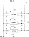
- the first stage 401 of the stages 401, 402, 403, ... may receive the start signal FLM, and each of the stages 402, 403, ... other than the first stage 401 may receive the emission control signal EM1, EM2, EM3, ... of a preceding stage.
- the ninth transistor M9 is coupled between the first power supply VDD and the output terminal 104.
- a gate electrode of the ninth transistor M9 may be coupled to the first node N1.
- the ninth transistor M9 may be turned on or off depending on the voltage of the first node N1.
- the voltage of the first power supply VDD that is supplied to the output terminal 104 when the ninth transistor M9 is turned on may be supplied to an i-th emission control line Ei and used as an emission control signal EM[i] having a gate-on level.
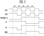
- the start signal FLM or the emission control signal EM[i-1] of the preceding stage to be supplied to the first input terminal 101 may be set to overlap at least once with the first clock signal CLK1 to be supplied to the second input terminal 102.
- the start signal FLM (or the emission control signal EM[i-1] of the preceding stage) may have a width greater than that of the first clock signal CLK1 and, for example, be supplied during four horizontal periods (4H).
- a first emission control signal to be supplied to the first input terminal 101 of the following stage may also overlap at least once with the second clock signal CLK2 to be supplied to the second input terminal 102 of the following stage.
- the start signal FLM or the emission control signal EM[i-1] of the preceding stage may be supplied to the first input terminal 101, and the first clock signal CLK1 may be supplied to the second input terminal 102.
- the first clock signal CLK1 is supplied to the second input terminal 102, the first transistor M1 and the fifth transistor M5 may be turned on.
- the sixth transistor M6 If the sixth transistor M6 is turned on, the third input terminal 103 and the sixth node N6 may be electrically coupled to each other. Since the second clock signal CLK2 is not supplied to the third input terminal 103 during the third period t3, the sixth node N6 may be maintained at the high voltage. Here, since the seventh transistor M7 remains turned off, the voltage of the sixth node N6 may not affect the voltage of the first node N1.
- the second capacitor C2 may store a voltage corresponding to the turn-on level of the sixth transistor M6.
- the third capacitor C3 may not be used as a load. Consequently, the power consumption may be reduced, and reliable output of the emission control signal EM[i] may be secured.
- the substrate SUB may be formed of a rigid substrate or a flexible substrate.
- the rigid substrate may include a glass substrate, a quartz substrate, a glass ceramic substrate, and a crystalline glass substrate.
- a first gate insulating layer GI1 may cover the active layer ACT.
- the first gate insulating layer GI1 may cover source electrodes SE1 to SE12, drain electrodes DEI to DE12, and channels (e.g., CH10) of the transistors M1 to M12.
- the first gate insulating layer GI1 may be an inorganic insulating layer.
- the first gate insulating layer GI1 may be formed of silicon nitride (SiN x ), silicon oxide (SiO x ), silicon oxynitride (SiO x N y ), or a combination thereof.
Landscapes
- Engineering & Computer Science (AREA)
- Physics & Mathematics (AREA)
- Computer Hardware Design (AREA)
- General Physics & Mathematics (AREA)
- Theoretical Computer Science (AREA)
- Control Of Indicators Other Than Cathode Ray Tubes (AREA)
- Logic Circuits (AREA)
- Electronic Switches (AREA)
- Microelectronics & Electronic Packaging (AREA)
Priority Applications (1)
| Application Number | Priority Date | Filing Date | Title |
|---|---|---|---|
| EP25209904.9A EP4657441A3 (de) | 2019-03-18 | 2020-03-18 | Stufe und emissionssteuerungstreiber damit |
Applications Claiming Priority (1)
| Application Number | Priority Date | Filing Date | Title |
|---|---|---|---|
| KR1020190030721A KR102718913B1 (ko) | 2019-03-18 | 2019-03-18 | 스테이지 및 이를 포함하는 발광 제어 구동부 |
Related Child Applications (2)
| Application Number | Title | Priority Date | Filing Date |
|---|---|---|---|
| EP25209904.9A Division EP4657441A3 (de) | 2019-03-18 | 2020-03-18 | Stufe und emissionssteuerungstreiber damit |
| EP25209904.9A Division-Into EP4657441A3 (de) | 2019-03-18 | 2020-03-18 | Stufe und emissionssteuerungstreiber damit |
Publications (3)
| Publication Number | Publication Date |
|---|---|
| EP3712878A2 true EP3712878A2 (de) | 2020-09-23 |
| EP3712878A3 EP3712878A3 (de) | 2020-10-07 |
| EP3712878B1 EP3712878B1 (de) | 2025-12-03 |
Family
ID=69845936
Family Applications (2)
| Application Number | Title | Priority Date | Filing Date |
|---|---|---|---|
| EP20163919.2A Active EP3712878B1 (de) | 2019-03-18 | 2020-03-18 | Stufe und emissionssteuerungstreiber damit |
| EP25209904.9A Pending EP4657441A3 (de) | 2019-03-18 | 2020-03-18 | Stufe und emissionssteuerungstreiber damit |
Family Applications After (1)
| Application Number | Title | Priority Date | Filing Date |
|---|---|---|---|
| EP25209904.9A Pending EP4657441A3 (de) | 2019-03-18 | 2020-03-18 | Stufe und emissionssteuerungstreiber damit |
Country Status (4)
| Country | Link |
|---|---|
| US (4) | US11557252B2 (de) |
| EP (2) | EP3712878B1 (de) |
| KR (3) | KR102718913B1 (de) |
| CN (2) | CN111710294B (de) |
Families Citing this family (9)
| Publication number | Priority date | Publication date | Assignee | Title |
|---|---|---|---|---|
| JP2013093565A (ja) | 2011-10-07 | 2013-05-16 | Semiconductor Energy Lab Co Ltd | 半導体装置 |
| KR102669165B1 (ko) | 2019-11-05 | 2024-05-28 | 삼성디스플레이 주식회사 | 발광 제어 구동부 및 이를 포함하는 표시 장치 |
| KR102724666B1 (ko) * | 2019-12-23 | 2024-11-04 | 삼성디스플레이 주식회사 | 발광 구동부 및 이를 포함하는 표시 장치 |
| CN111768733B (zh) * | 2020-06-10 | 2022-08-30 | 京东方科技集团股份有限公司 | 发光控制信号生成电路、方法和显示装置 |
| EP4539052A1 (de) * | 2020-09-30 | 2025-04-16 | BOE Technology Group Co., Ltd. | Anzeigesubstrat und herstellungsverfahren dafür sowie anzeigevorrichtung |
| CN112365846B (zh) * | 2020-11-12 | 2021-10-08 | 深圳市华星光电半导体显示技术有限公司 | 像素电路及显示装置 |
| WO2023070647A1 (en) * | 2021-11-01 | 2023-05-04 | Boe Technology Group Co., Ltd. | Scan circuit and display apparatus |
| CN115458818B (zh) * | 2022-08-25 | 2024-05-14 | 圣邦微电子(北京)股份有限公司 | 适用于多种类型的电池包的电流采样电路 |
| CN118824170A (zh) * | 2024-08-29 | 2024-10-22 | 厦门天马显示科技有限公司 | 一种栅极驱动电路、显示面板及显示装置 |
Family Cites Families (14)
| Publication number | Priority date | Publication date | Assignee | Title |
|---|---|---|---|---|
| CN102783025B (zh) * | 2010-03-02 | 2015-10-07 | 株式会社半导体能源研究所 | 脉冲信号输出电路和移位寄存器 |
| KR101975581B1 (ko) | 2012-08-21 | 2019-09-11 | 삼성디스플레이 주식회사 | 발광 제어 구동부 및 그것을 포함하는 유기발광 표시장치 |
| KR102081910B1 (ko) | 2013-06-12 | 2020-02-27 | 삼성디스플레이 주식회사 | 커패시터, 커패시터를 포함하는 구동 회로, 및 구동 회로를 포함하는 표시 장치 |
| KR102061256B1 (ko) | 2013-08-29 | 2020-01-03 | 삼성디스플레이 주식회사 | 스테이지 회로 및 이를 이용한 유기전계발광 표시장치 |
| KR20150081872A (ko) * | 2014-01-07 | 2015-07-15 | 삼성디스플레이 주식회사 | 표시 장치 |
| CN103943081A (zh) * | 2014-03-14 | 2014-07-23 | 京东方科技集团股份有限公司 | 移位寄存器、其制作方法、栅线集成驱动电路及相关装置 |
| CN105047172A (zh) * | 2015-09-15 | 2015-11-11 | 京东方科技集团股份有限公司 | 移位寄存器、栅极驱动电路、显示屏及其驱动方法 |
| KR102477486B1 (ko) * | 2016-04-19 | 2022-12-14 | 삼성디스플레이 주식회사 | 발광 제어 구동 장치 및 이를 포함하는 표시 장치 |
| KR102463953B1 (ko) * | 2016-05-25 | 2022-11-08 | 삼성디스플레이 주식회사 | 발광 제어 구동부 및 이를 포함하는 표시 장치 |
| KR102511947B1 (ko) | 2016-06-17 | 2023-03-21 | 삼성디스플레이 주식회사 | 스테이지 및 이를 이용한 유기전계발광 표시장치 |
| JP2018093483A (ja) * | 2016-11-29 | 2018-06-14 | 株式会社半導体エネルギー研究所 | 半導体装置、表示装置及び電子機器 |
| KR102519539B1 (ko) * | 2017-05-15 | 2023-04-11 | 삼성디스플레이 주식회사 | 스테이지 및 이를 이용한 주사 구동부 |
| US10643533B2 (en) | 2018-01-19 | 2020-05-05 | Kunshan Go-Visionox Opto-Electronics Co., Ltd. | Emission control driving circuit, emission control driver and organic light emitting display device |
| CN108399887B (zh) * | 2018-03-28 | 2019-09-27 | 上海天马有机发光显示技术有限公司 | 移位寄存器及其驱动方法、发射驱动电路和显示装置 |
-
2019
- 2019-03-18 KR KR1020190030721A patent/KR102718913B1/ko active Active
-
2020
- 2020-03-17 US US16/821,490 patent/US11557252B2/en active Active
- 2020-03-17 CN CN202010186275.4A patent/CN111710294B/zh active Active
- 2020-03-17 CN CN202510816181.3A patent/CN120823795A/zh active Pending
- 2020-03-18 EP EP20163919.2A patent/EP3712878B1/de active Active
- 2020-03-18 EP EP25209904.9A patent/EP4657441A3/de active Pending
-
2022
- 2022-09-07 US US17/939,926 patent/US11915653B2/en active Active
-
2024
- 2024-02-20 US US18/582,592 patent/US20240290273A1/en active Pending
- 2024-09-25 US US18/895,664 patent/US20250014519A1/en active Pending
- 2024-10-14 KR KR1020240139488A patent/KR102808382B1/ko active Active
-
2025
- 2025-05-12 KR KR1020250061170A patent/KR20250076468A/ko active Pending
Also Published As
| Publication number | Publication date |
|---|---|
| US20200302870A1 (en) | 2020-09-24 |
| CN111710294B (zh) | 2025-07-08 |
| KR102718913B1 (ko) | 2024-10-18 |
| US20230005428A1 (en) | 2023-01-05 |
| US20250014519A1 (en) | 2025-01-09 |
| KR20240153543A (ko) | 2024-10-23 |
| EP4657441A2 (de) | 2025-12-03 |
| CN120823795A (zh) | 2025-10-21 |
| KR20250076468A (ko) | 2025-05-29 |
| US20240290273A1 (en) | 2024-08-29 |
| US11915653B2 (en) | 2024-02-27 |
| EP3712878A3 (de) | 2020-10-07 |
| KR102808382B1 (ko) | 2025-05-19 |
| EP4657441A3 (de) | 2026-02-18 |
| KR20200111322A (ko) | 2020-09-29 |
| CN111710294A (zh) | 2020-09-25 |
| EP3712878B1 (de) | 2025-12-03 |
| US11557252B2 (en) | 2023-01-17 |
Similar Documents
| Publication | Publication Date | Title |
|---|---|---|
| EP3712878B1 (de) | Stufe und emissionssteuerungstreiber damit | |
| US11302255B2 (en) | Display apparatus | |
| US11450281B2 (en) | Stage and scan driver including the same | |
| CN110364125B (zh) | 扫描驱动器 | |
| CN110853583A (zh) | 扫描驱动器和具有该扫描驱动器的显示装置 | |
| CN119811310A (zh) | 显示装置 | |
| US11195469B2 (en) | Stage for a display device and scan driver having the same | |
| US11514840B2 (en) | Light emission control driver and display device including the same | |
| CN114648947A (zh) | 扫描驱动器及其驱动方法 | |
| EP3651145B1 (de) | Pixelschaltung | |
| US11521570B2 (en) | Gate driver and display device including the same | |
| US11756477B2 (en) | Gate driver and display device including the same | |
| US20250148979A1 (en) | Display device | |
| US20240321215A1 (en) | Gate driving circuit | |
| US11723247B2 (en) | Display device | |
| KR20250131310A (ko) | 구동회로 | |
| US20250273164A1 (en) | Driving circuit | |
| US12243491B2 (en) | Display panel | |
| CN118692386A (zh) | 驱动电路 |
Legal Events
| Date | Code | Title | Description |
|---|---|---|---|
| PUAI | Public reference made under article 153(3) epc to a published international application that has entered the european phase |
Free format text: ORIGINAL CODE: 0009012 |
|
| STAA | Information on the status of an ep patent application or granted ep patent |
Free format text: STATUS: THE APPLICATION HAS BEEN PUBLISHED |
|
| PUAL | Search report despatched |
Free format text: ORIGINAL CODE: 0009013 |
|
| AK | Designated contracting states |
Kind code of ref document: A2 Designated state(s): AL AT BE BG CH CY CZ DE DK EE ES FI FR GB GR HR HU IE IS IT LI LT LU LV MC MK MT NL NO PL PT RO RS SE SI SK SM TR |
|
| AX | Request for extension of the european patent |
Extension state: BA ME |
|
| AK | Designated contracting states |
Kind code of ref document: A3 Designated state(s): AL AT BE BG CH CY CZ DE DK EE ES FI FR GB GR HR HU IE IS IT LI LT LU LV MC MK MT NL NO PL PT RO RS SE SI SK SM TR |
|
| AX | Request for extension of the european patent |
Extension state: BA ME |
|
| RIC1 | Information provided on ipc code assigned before grant |
Ipc: H01L 27/32 20060101ALN20200901BHEP Ipc: G11C 19/28 20060101ALN20200901BHEP Ipc: G09G 3/3266 20160101AFI20200901BHEP |
|
| STAA | Information on the status of an ep patent application or granted ep patent |
Free format text: STATUS: REQUEST FOR EXAMINATION WAS MADE |
|
| 17P | Request for examination filed |
Effective date: 20210406 |
|
| RBV | Designated contracting states (corrected) |
Designated state(s): AL AT BE BG CH CY CZ DE DK EE ES FI FR GB GR HR HU IE IS IT LI LT LU LV MC MK MT NL NO PL PT RO RS SE SI SK SM TR |
|
| STAA | Information on the status of an ep patent application or granted ep patent |
Free format text: STATUS: EXAMINATION IS IN PROGRESS |
|
| 17Q | First examination report despatched |
Effective date: 20221107 |
|
| P01 | Opt-out of the competence of the unified patent court (upc) registered |
Effective date: 20230516 |
|
| GRAP | Despatch of communication of intention to grant a patent |
Free format text: ORIGINAL CODE: EPIDOSNIGR1 |
|
| STAA | Information on the status of an ep patent application or granted ep patent |
Free format text: STATUS: GRANT OF PATENT IS INTENDED |
|
| RIC1 | Information provided on ipc code assigned before grant |
Ipc: G09G 3/3266 20160101AFI20250610BHEP Ipc: G11C 19/28 20060101ALN20250610BHEP |
|
| INTG | Intention to grant announced |
Effective date: 20250625 |
|
| GRAS | Grant fee paid |
Free format text: ORIGINAL CODE: EPIDOSNIGR3 |
|
| GRAA | (expected) grant |
Free format text: ORIGINAL CODE: 0009210 |
|
| STAA | Information on the status of an ep patent application or granted ep patent |
Free format text: STATUS: THE PATENT HAS BEEN GRANTED |
|
| AK | Designated contracting states |
Kind code of ref document: B1 Designated state(s): AL AT BE BG CH CY CZ DE DK EE ES FI FR GB GR HR HU IE IS IT LI LT LU LV MC MK MT NL NO PL PT RO RS SE SI SK SM TR |
|
| REG | Reference to a national code |
Ref country code: CH Ref legal event code: F10 Free format text: ST27 STATUS EVENT CODE: U-0-0-F10-F00 (AS PROVIDED BY THE NATIONAL OFFICE) Effective date: 20251203 Ref country code: GB Ref legal event code: FG4D |
|
| REG | Reference to a national code |
Ref country code: DE Ref legal event code: R096 Ref document number: 602020063082 Country of ref document: DE |
|
| REG | Reference to a national code |
Ref country code: IE Ref legal event code: FG4D |
|
| REG | Reference to a national code |
Ref country code: NL Ref legal event code: FP |
|
| PGFP | Annual fee paid to national office [announced via postgrant information from national office to epo] |
Ref country code: NL Payment date: 20260220 Year of fee payment: 7 |