EP3712962A1 - Diode mps semiconductrice avec réduction de l'effet de tassement de courant et son procédé de fabrication - Google Patents
Diode mps semiconductrice avec réduction de l'effet de tassement de courant et son procédé de fabrication Download PDFInfo
- Publication number
- EP3712962A1 EP3712962A1 EP20164124.8A EP20164124A EP3712962A1 EP 3712962 A1 EP3712962 A1 EP 3712962A1 EP 20164124 A EP20164124 A EP 20164124A EP 3712962 A1 EP3712962 A1 EP 3712962A1
- Authority
- EP
- European Patent Office
- Prior art keywords
- doped region
- cells
- drift layer
- forming
- diode
- Prior art date
- Legal status (The legal status is an assumption and is not a legal conclusion. Google has not performed a legal analysis and makes no representation as to the accuracy of the status listed.)
- Granted
Links
Images


Classifications
-
- H—ELECTRICITY
- H10—SEMICONDUCTOR DEVICES; ELECTRIC SOLID-STATE DEVICES NOT OTHERWISE PROVIDED FOR
- H10D—INORGANIC ELECTRIC SEMICONDUCTOR DEVICES
- H10D8/00—Diodes
- H10D8/60—Schottky-barrier diodes
-
- H—ELECTRICITY
- H10—SEMICONDUCTOR DEVICES; ELECTRIC SOLID-STATE DEVICES NOT OTHERWISE PROVIDED FOR
- H10D—INORGANIC ELECTRIC SEMICONDUCTOR DEVICES
- H10D62/00—Semiconductor bodies, or regions thereof, of devices having potential barriers
- H10D62/10—Shapes, relative sizes or dispositions of the regions of the semiconductor bodies; Shapes of the semiconductor bodies
- H10D62/102—Constructional design considerations for preventing surface leakage or controlling electric field concentration
- H10D62/103—Constructional design considerations for preventing surface leakage or controlling electric field concentration for increasing or controlling the breakdown voltage of reverse-biased devices
- H10D62/105—Constructional design considerations for preventing surface leakage or controlling electric field concentration for increasing or controlling the breakdown voltage of reverse-biased devices by having particular doping profiles, shapes or arrangements of PN junctions; by having supplementary regions, e.g. junction termination extension [JTE]
- H10D62/106—Constructional design considerations for preventing surface leakage or controlling electric field concentration for increasing or controlling the breakdown voltage of reverse-biased devices by having particular doping profiles, shapes or arrangements of PN junctions; by having supplementary regions, e.g. junction termination extension [JTE] having supplementary regions doped oppositely to or in rectifying contact with regions of the semiconductor bodies, e.g. guard rings with PN or Schottky junctions
-
- H—ELECTRICITY
- H10—SEMICONDUCTOR DEVICES; ELECTRIC SOLID-STATE DEVICES NOT OTHERWISE PROVIDED FOR
- H10D—INORGANIC ELECTRIC SEMICONDUCTOR DEVICES
- H10D62/00—Semiconductor bodies, or regions thereof, of devices having potential barriers
- H10D62/10—Shapes, relative sizes or dispositions of the regions of the semiconductor bodies; Shapes of the semiconductor bodies
- H10D62/117—Shapes of semiconductor bodies
- H10D62/118—Nanostructure semiconductor bodies
-
- H—ELECTRICITY
- H10—SEMICONDUCTOR DEVICES; ELECTRIC SOLID-STATE DEVICES NOT OTHERWISE PROVIDED FOR
- H10D—INORGANIC ELECTRIC SEMICONDUCTOR DEVICES
- H10D62/00—Semiconductor bodies, or regions thereof, of devices having potential barriers
- H10D62/10—Shapes, relative sizes or dispositions of the regions of the semiconductor bodies; Shapes of the semiconductor bodies
- H10D62/124—Shapes, relative sizes or dispositions of the regions of semiconductor bodies or of junctions between the regions
- H10D62/126—Top-view geometrical layouts of the regions or the junctions
-
- H—ELECTRICITY
- H10—SEMICONDUCTOR DEVICES; ELECTRIC SOLID-STATE DEVICES NOT OTHERWISE PROVIDED FOR
- H10D—INORGANIC ELECTRIC SEMICONDUCTOR DEVICES
- H10D62/00—Semiconductor bodies, or regions thereof, of devices having potential barriers
- H10D62/80—Semiconductor bodies, or regions thereof, of devices having potential barriers characterised by the materials
- H10D62/83—Semiconductor bodies, or regions thereof, of devices having potential barriers characterised by the materials being Group IV materials, e.g. B-doped Si or undoped Ge
- H10D62/832—Semiconductor bodies, or regions thereof, of devices having potential barriers characterised by the materials being Group IV materials, e.g. B-doped Si or undoped Ge being Group IV materials comprising two or more elements, e.g. SiGe
- H10D62/8325—Silicon carbide
-
- H—ELECTRICITY
- H10—SEMICONDUCTOR DEVICES; ELECTRIC SOLID-STATE DEVICES NOT OTHERWISE PROVIDED FOR
- H10D—INORGANIC ELECTRIC SEMICONDUCTOR DEVICES
- H10D64/00—Electrodes of devices having potential barriers
- H10D64/60—Electrodes characterised by their materials
- H10D64/62—Electrodes ohmically coupled to a semiconductor
-
- H—ELECTRICITY
- H10—SEMICONDUCTOR DEVICES; ELECTRIC SOLID-STATE DEVICES NOT OTHERWISE PROVIDED FOR
- H10D—INORGANIC ELECTRIC SEMICONDUCTOR DEVICES
- H10D64/00—Electrodes of devices having potential barriers
- H10D64/60—Electrodes characterised by their materials
- H10D64/64—Electrodes comprising a Schottky barrier to a semiconductor
-
- H—ELECTRICITY
- H10—SEMICONDUCTOR DEVICES; ELECTRIC SOLID-STATE DEVICES NOT OTHERWISE PROVIDED FOR
- H10D—INORGANIC ELECTRIC SEMICONDUCTOR DEVICES
- H10D8/00—Diodes
- H10D8/01—Manufacture or treatment
- H10D8/051—Manufacture or treatment of Schottky diodes
-
- H—ELECTRICITY
- H10—SEMICONDUCTOR DEVICES; ELECTRIC SOLID-STATE DEVICES NOT OTHERWISE PROVIDED FOR
- H10D—INORGANIC ELECTRIC SEMICONDUCTOR DEVICES
- H10D62/00—Semiconductor bodies, or regions thereof, of devices having potential barriers
- H10D62/80—Semiconductor bodies, or regions thereof, of devices having potential barriers characterised by the materials
- H10D62/85—Semiconductor bodies, or regions thereof, of devices having potential barriers characterised by the materials being Group III-V materials, e.g. GaAs
- H10D62/8503—Nitride Group III-V materials, e.g. AlN or GaN
Definitions
- the present invention relates to a semiconductor MPS diode with reduced current-crowding effect and a manufacturing method thereof.
- the present invention relates to an electronic device based on silicon carbide, provided having an active area designed to minimise the crowding of electric current which flows during use from the anode to the cathode.
- semiconductor materials which have a wide forbidden band gap, in particular, which have an energy value Eg of the forbidden band gap greater than 1.1 eV, low on-state resistance (R ON ), high value of thermal conductivity, high operating frequency, and high velocity saturation of charge carriers, are ideal for producing electronic components, such as diodes or transistors, in particular for power applications.
- a material having said characteristics, and designed to be used manufacturing electronic components is silicon carbide (SiC).
- SiC silicon carbide
- silicon carbide in its different polytypes (e.g., 3C-SiC, 4H-SiC, 6H-SiC), is preferable to silicon as regards the properties listed previously.
- Electronic devices provided on a silicon-carbide substrate as compared to similar devices provided on a silicon substrate, present numerous advantages, such as low output resistance in conduction, low leakage current, high working temperature, and high working frequencies.
- SiC Schottky diodes demonstrated superior switching performance, which renders SiC power devices especially favorable for high-frequency applications.
- Today's applications pose requirements on the electrical properties as well as on the long-term reliability of the devices.
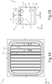
- Figure 1A shows, in top-plan view in a Cartesian (triaxial) reference system of axis X, Y, Z, a merged-PN-Schottky (MPS) device 1 of a known type.
- Figure 1B shows, in the same reference system, a lateral sectional view taken along line I-I, a portion of the MPS device 1.
- MPS merged-PN-Schottky
- the MPS device 1 includes: a substrate 3, of N-type SiC, having a first dopant concentration; a drift layer (epitaxially grown) 2, of N-type SiC, having a second dopant concentration lower than the first dopant concentration, extending on surface 3a of the substrate 3; a cathode terminal 6, of metal material, extending on surface 3b (opposite to surface 3a) of the substrate 3; an anode terminal 8, of metal material (anode metallization), extending on a top surface 2a the drift layer 2; a plurality of junction-barrier (JB) elements 9 in the drift layer 2, facing the top surface 2a of the drift layer 2, and including each a respective implanted region 9' of P-type and a ohmic contact 9" of metal material; and an edge termination region (guard ring) 10, in particular an implanted region of P-type, completely surrounding the junction-barrier (JB) elements 9.
- a substrate 3, of N-type SiC having a first dopant concentration
- Schottky diodes 12 are formed at the interface between the drift layer 2 and the metallization of the anode metallization 8.
- Schottky junctions metal-semiconductor
- portions of the drift layer 2 in direct electrical contact with respective portions of the anode metallization 8.
- the region of the MPS device 1 including the JB elements 9 and the Schottky diodes 12 is an active area 14 of the MPS device 1.
- MPS device 1 During use in the forward conducting state, due to the lower Schottky onset (about 0.7 V) than the PN onset (about 2.5 V), MPS device 1 functions as a Schottky diode at lower current densities (low on-state losses) and assumes the characteristic of a PN-diode at higher enough current densities.
- the asymmetric layout of Figure 1A induces a current-crowding effect in the active area 14 at the corners / rounded regions close to the intersection between the implanted regions 9' and the guard ring 10. Specifically, the corners in the active area 14 concentrate the current at a higher density than the rest of the active area 14.
- the bipolar conduction tends to be enabled first in these zones because of the higher voltage drop due to the higher current density and because of the higher temperature due to self-heating effect.
- Thermal runaway on very limited regions causes the formation of hot spots having a temperature that reaches high values, up to the material melting point, thus inducing a failure of the device or thermo-mechanical stresses that may ultimately lead to cracks in the die.
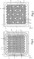
- FIG. 2 shows, in a top-plan view in the X, Y, Z reference system, an embodiment where the JB elements 9 are in the form of cells or dots, and include each an implanted region 9' having an hexagonal shape, with a respective ohmic contacts 9" formed within the implanted region 9'.
- the JB elements 9 are organized in a symmetrical array.
- the ohmic contacts are discontinuous.
- the Schottky diode 12 is formed by the drift layer 2 surrounding the JB elements 9 and the anode metallization 8 extending above the drift layer 2.
- FIG. 3 shows, in a top-plan view in the X, Y, Z reference system, an embodiment where both the Schottky diodes 12 and the JB elements 9 are in the form of cells or dots having an hexagonal shape. More in particular, each JB element 9 is completely surrounded by a respective Schottky diode 12; moreover, each Schottky diode 12 is completely surrounded (in top-plan view), and separated from ad adjacent Schottky diode 12, by a P+ region.
- the aim of the present invention is to provide a MPS diode with reduced current-crowding effect and a manufacturing method thereof, to overcome the drawbacks of the prior art.
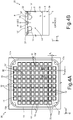
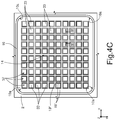
- Figure 4A shows, in the same reference system of axis X, Y, Z of Figures 1A-3 , a top-plan view (i.e., on XY plane) of a Merged-PN-Schottky (MPS) device 30 (in particular, a MPS diode), according to an embodiment of the present invention.
- Figure 4B shows, in the same reference system, a lateral sectional view taken along line IV-IV of Figure 4A .
- the anode metallization 8 is not shown, even if present, as apparent from the view of Figure 4B .
- each Schottky diode 32 of a plurality of Schottky diodes 32 includes a respective Schottky cell (or dot) 33 having, in top-plan view on XY plane, a squared shape; the Schottky cells 33 are arranged in a grid-like pattern, in particular forming a symmetric array of Schottky cells 33. Still more in particular, each Schottky cell 33 includes a superficial region of the drift layer 2 of N type of conductivity and N-doping concentration. The Schottky cells 33 are separated from one another, along X and Y directions, by implanted regions 19', of P conductivity type, extending in the drift layer 2.
- Each implanted region 19' separating one Schottky cell 33 from another, along both X and Y directions, is electrically connected to the other implanted regions 19', thus forming a continuous grid of implanted regions, which are therefore completely connected to one another.
- the implanted regions 19' form a set of squares, each square being one Schottky cell 33.
- Each Schottky cell 33 is thus completely surrounded, in top-plan view, by a respective one of the implanted regions 19'.
- Each implanted region 19' laterally surrounding one Schottky cell 33 is electrically connected to the other implanted regions 19' underneath the ohmic contacts 19" as shown in Figure 4B .
- the implanted regions 19' form a continuous grid extending under the grid of ohmic contacts 19".
- the implanted regions 19' include stripes along the X-axis direction that cross stripes along the Y-axis direction, to make a set of squares, each square being one Schottky cell 33.
- Each Schottky cell 33 is thus completely surrounded, in top-plan view, by the implanted regions 19'.
- each Schottky cell 33 is separated from an adjacent Schottky cell 33, along the X-axis direction, by a distance dx in the range 0.5pm-5pm; each Schottky cell 33 is separated from an adjacent Schottky cell 33, along the Y-axis direction, by a distance d Y in the range 0.5pm-5pm.
- distances d x and dy are equal to one another.
- the portion of the MPS device 30 where the Schottky cells 33 are formed is the active area 14 of the MPS device 30.
- a guard ring, or edge-termination region, 10, completely surrounding the active area 14, is also optionally present.
- the guard ring 10 extends as continuation of the implanted regions 19'.
- the implanted regions 19' and the guard ring 10 are connected to one another without any discontinuity. It is apparent that a continuous guard ring 10, completely surrounding the active area 14, may be omitted; in this case, the implanted regions 19' ends at the outer edges of the active area 14.
- the Schottky cells 33 form, with the anode metallization 8 extending above them and in direct electrical contact with them, the Schottky diodes 32 graphically represented in Figure 4B .
- the layout in top-plan view of the MPS device 30 is symmetric with respect to any line of symmetry passing through the centroid of the geometric shape delimited by the guard ring 10.
- the layout in top-plan view of the MPS device 30 is symmetric with respect to any line of symmetry passing through the centroid of the geometric figure delimited by the outer edges of the grid-like pattern (array) of Schottky cells 33 or, analogously, of the outer edges of the active area 14.
- guard ring 10 in Figure 4A has a quadrangular shape with rounded corners 10a.
- Schottky cells are not present at said rounded corners 10a.
- the guard ring 10 may be moved away from the active area 14, increasing the dimensions of the device 30 but avoiding the undesired current-crowding effect at the corners 10a).
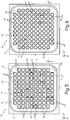
- FIG. 5 shows an embodiment of an MPS device 30' where Schottky cells 33', which correspond in terms of functions to the Schottky cells 33 of MPS device 30, have each a quadrangular shape with rounded corners.
- Other elements of the MPS device 30' in common with elements of the MPS device 30 are identified with the same reference numerals and not further described.
- the cross sectional view of MPS device 30', taken along the line IV-IV in Figure 5 correspond to that of Figure 4B and therefore is not shown.
- FIG. 6 shows an embodiment of an MPS device 30" where Schottky cells 33", which correspond in terms of functions to the Schottky cells 33 of MPS device 30, have each a circular shape.
- Other elements of the MPS device 30" in common with elements of the MPS device 30 are identified with the same reference numerals and not further described.
- a method is also provided for manufacturing the MPS device 30 (reference can be made to Figures 7-11 ).
- the method disclosed herein can be also applied to manufacture the MPS device 30' and MPS device 30" of Figures 4 and 5 .
- Figures 7-11 illustrate, in lateral sectional view, steps of processing of a wafer 100 of semiconductor material.
- Figures 7-11 show the wafer 100 in the triaxial system of mutually orthogonal axes X, Y, Z of Figures 4A-4B .
- the wafer 100 comprises the substrate 3 of semiconductor material, in particular silicon carbide (SiC) having a first conductivity type (in this embodiment a doping of an N type), provided with a front side 3a and a back side 3b that are opposite to one another along the Z axis.
- the resistivity of the substrate 30 is, for example, comprised between 5 m ⁇ cm and 40 m ⁇ cm.
- the drift layer 2 On the front side 3a of the substrate 3, it is formed, for example by epitaxial growth, the drift layer 2, of silicon carbide having the first conductivity type (N) and having a concentration of dopants lower than that of the substrate 3, for example comprised between 1 ⁇ 10 14 and 5 ⁇ 10 16 atoms/cm 3 .
- the drift layer 2 is made of SiC, in particular 4H-SiC, but other polytypes may be used, such as 2H, 6H, 3C, and/or 15R.
- the substrate 3 and the drift layer 2 may be made of other semiconductor materials, for example GaN, GaAs, Ge.
- the drift layer 2 extends between a top side 2a and a bottom side 2b (the latter in direct contact with the front side 3a of the substrate 3).
- a hard mask 50 is formed, for example by deposition of photoresist, or TEOS, or other material.
- the hard mask 50 has a thickness of between 0.5 ⁇ m and 2 ⁇ m, or in any case a thickness such as to shield the implantation described hereinafter with reference to the same Figure 8 .
- the hard mask 34 thus formed extends in a region of the wafer 100 where, in subsequent steps, the active area 14 of the MPS device 30 will be formed.
- the hard mask 50 covers the regions of the top side 2a of drift layer 2 which will form the Schottky cells 33 and leaves exposed regions of the top side 2a of drift layer 2 which will form the implanted regions 19', identified with reference to Figures 4A and 4B .
- a step is now carried out of implantation of dopant species (e.g., boron or aluminium), which have the second conductivity type (here, P), exploiting the hard mask 50 (the implantation is indicated in the figure by arrows 52).
- dopant species e.g., boron or aluminium
- P the second conductivity type
- the guard ring 10 if present, is also formed.
- the step of Figure 8 comprises one or more implantations of dopant species, which have the second type of conductivity, with implantation energy comprised between 30 keV and 400 keV, and with doses of between 1 ⁇ 10 12 atoms/cm 2 and 1 ⁇ 10 15 atoms/cm 2 , in order to form the implanted regions 19' with dopant concentration higher than 1 ⁇ 10 18 atoms/cm 3 .
- the mask 50 is removed and a step of thermal annealing is carried out for diffusion and activation of the dopant species implanted in the step of Figure 8 .
- the thermal annealing is, for example, carried out at a temperature higher than 1600°C (e.g., between 1700 and 1900 °C, and in some cases even higher).
- the implanted regions 19' have a concentration of dopant species comprised between approximately 1 ⁇ 10 17 atoms/cm 3 and 1 ⁇ 10 20 atoms/cm 3 . Implanted regions 19' are thus formed.
- Schottky cells 33 are formed, that are the portions of the drift layer 2 which extends laterally to the implanted regions 19' or, in other words, the portions of the drift layer 2 of N-type masked during the implantation step of Figure 8 .
- Ohmic contacts 19" (e.g., of Nickel Silicide - Ni 2 Si) are then formed at each implanted region 19', thus concurring to the formation of respective JB elements 19. It is noted that implanted regions 19' visible in the cross sectional view are actually one uniform region, as it can be appreciated from the top view of Figure 4A . Accordingly, also ohmic contacts 19" are formed as one contact electrically connected to the implanted regions 19'. Therefore, the Schottky cells 33 are also separated from one another, along X and Y directions, by ohmic contacts 19" extending on the implanted regions 19'. As discussed above, the ohmic contacts 19" form a continuous grid overlying the grid of implanted regions and are therefore completely connected to one another.
- the ohmic contacts 19" form a continuous grid overlying the grid of implanted regions and are therefore completely connected to one another.
- An ohmic contact is also formed at the guard ring 10, electrically connected to the ohmic contacts 19".
- the formation of ohmic contacts 19" includes forming a hard mask of thin oxide (e.g., in the range of 100pm - 500pm); then photolithography and etching steps are performed to etch the regions where ohmic contacts 19" are to be formed; then, a deposition of metal material is carried out and a subsequent thermal treatment is performed (e.g., at a temperature in the range 900°C - 1100°C for a time interval in the range 10 minutes - 120 minutes).
- the metal thus deposited reacts with the superficial SiC material forming Ni2Si (i.e., the ohmic contact), while the metal in contact with the oxide does not react.
- a step of removal of the non-reacted metal is carried out and, then, a step of removal of the oxide metal is carried out.
- an interface layer 57 of metal material such as titanium, nickel, molybdenum, is deposited on the drift layer 2.
- the interface layer 57 is deposited via sputtering and has a thickness of between approximately 10 nm and 500 nm.
- the interface layer 57 extends in contact with the implanted regions 19' through the ohmic contacts 19", and with the exposed regions 33 of the drift layer 32 between the ohmic contacts 19" (i.e., the Schottky cells 33).
- the interface layer 57 contributes to the formation of a Schottky contact/Schottky barrier with the exposed regions 33 of the drift layer 32 and to the formation of junction-barrier (JB) elements with the implanted regions 19' through the ohmic contacts 19".
- JB junction-barrier
- the metal layer 58 is, for example, of aluminium or copper, and has a thickness of a few microns, for example between 1 and 10 ⁇ m.
- the ensemble constituted by the interface layer 57 and the metal layer 58 forms the anode metallization reference as 8 in Figure 4B .
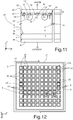
- a plurality of metal-semiconductor junctions of a Schottky type 32 are thus formed between the anode metallization 8 and the regions of the drift layer 2 that have the first conductivity type (N), as represented in Figure 11 .
- the interface layer 57 is omitted, so that the anode metallization 8 coincides with the metal layer 58, which extends in direct contact with the drift layer 2.
- cathode contact 6 is formed on the back side 3b of the substrate 3, for example by depositing a layer of metal material adapted to form an ohmic contact with the substrate 3.
- the region of the drift layer 2 that extends along the axis Z between the Schottky junctions and the cathode is the active area 14 of the diode 30 (i.e., the region where drift of the electrical charges occurs).
- the guard ring 10 (not shown in figure 11 ) surrounds the active area 14.
- a plurality of MPS devices 30 are formed on the same wafer 100.
- a final step of die singulation is carried out to physically isolate one MPS device 30 from another.
- the MPS devices 30 of Figures 4A, 4B is thus formed.
- Figure 12 shows a further embodiment of the present invention, where the guard ring 10 has a quadrangular shape and Schottky cells 33 are also present at the inner corners of the guard ring 10.
Landscapes
- Electrodes Of Semiconductors (AREA)
Applications Claiming Priority (1)
| Application Number | Priority Date | Filing Date | Title |
|---|---|---|---|
| IT201900004195 | 2019-03-22 |
Publications (3)
| Publication Number | Publication Date |
|---|---|
| EP3712962A1 true EP3712962A1 (fr) | 2020-09-23 |
| EP3712962B1 EP3712962B1 (fr) | 2023-06-07 |
| EP3712962C0 EP3712962C0 (fr) | 2023-06-07 |
Family
ID=66776806
Family Applications (1)
| Application Number | Title | Priority Date | Filing Date |
|---|---|---|---|
| EP20164124.8A Active EP3712962B1 (fr) | 2019-03-22 | 2020-03-19 | Diode mps semiconductrice avec réduction de l'effet de tassement de courant et son procédé de fabrication |
Country Status (3)
| Country | Link |
|---|---|
| US (2) | US11417778B2 (fr) |
| EP (1) | EP3712962B1 (fr) |
| CN (2) | CN111725329B (fr) |
Cited By (1)
| Publication number | Priority date | Publication date | Assignee | Title |
|---|---|---|---|---|
| CN114242767A (zh) * | 2021-11-13 | 2022-03-25 | 深圳芯能半导体技术有限公司 | 一种mps二极管的制备方法及mps二极管 |
Families Citing this family (9)
| Publication number | Priority date | Publication date | Assignee | Title |
|---|---|---|---|---|
| EP3712962B1 (fr) * | 2019-03-22 | 2023-06-07 | STMicroelectronics S.r.l. | Diode mps semiconductrice avec réduction de l'effet de tassement de courant et son procédé de fabrication |
| IT202000004696A1 (it) * | 2020-03-05 | 2021-09-05 | St Microelectronics Srl | METODO DI FABBRICAZIONE DI UN DISPOSITIVO ELETTRONICO IN SiC CON FASI DI MANIPOLAZIONE RIDOTTE, E DISPOSITIVO ELETTRONICO IN SiC |
| IT202000008179A1 (it) | 2020-04-17 | 2021-10-17 | St Microelectronics Srl | Formazione di contatti ohmici in un dispositivo elettronico basato su sic, e dispositivo elettronico |
| IT202000008167A1 (it) | 2020-04-17 | 2021-10-17 | St Microelectronics Srl | Attivazione droganti e formazione di contatto ohmico in un dispositivo elettronico in sic, e dispositivo elettronico in sic |
| IT202000015100A1 (it) | 2020-06-23 | 2021-12-23 | St Microelectronics Srl | Metodo di fabbricazione di un dispositivo rivelatore di una radiazione uv basato su sic e dispositivo rivelatore di una radiazione uv basato su sic |
| IT202100002333A1 (it) * | 2021-02-03 | 2022-08-03 | St Microelectronics Srl | Dispositivo jbs con prestazioni elettriche migliorate, e processo di fabbricazione del dispositivo jbs |
| CN113990934B (zh) * | 2021-10-29 | 2023-07-28 | 西安微电子技术研究所 | 一种SiC JBS元胞结构及制备方法 |
| US12588302B2 (en) | 2023-05-16 | 2026-03-24 | Omnivision Technologies, Inc. | Backside deep trench isolation structure for leakage suppression |
| IT202300019941A1 (it) * | 2023-09-27 | 2025-03-27 | St Microelectronics Int Nv | Formazione di un contatto schottky in un dispositivo elettronico, quale un diodo jbs o mps, e dispositivo elettronico con contatto schottky |
Citations (5)
| Publication number | Priority date | Publication date | Assignee | Title |
|---|---|---|---|---|
| US20080277668A1 (en) * | 2007-05-10 | 2008-11-13 | Denso Corporation | SIS semiconductor having junction barrier schottky device |
| JP2011142355A (ja) * | 2011-04-21 | 2011-07-21 | Sumitomo Electric Ind Ltd | 整流素子 |
| US20130105819A1 (en) * | 2011-10-28 | 2013-05-02 | Hitachi, Ltd. | Semiconductor device |
| US9455326B2 (en) * | 2012-02-15 | 2016-09-27 | Fuji Electric Co., Ltd. | Wide bandgap semiconductor device |
| US20180190651A1 (en) * | 2017-01-04 | 2018-07-05 | Infineon Technologies Ag | Semiconductor Device and Corresponding Manufacturing Method |
Family Cites Families (11)
| Publication number | Priority date | Publication date | Assignee | Title |
|---|---|---|---|---|
| DE69841363D1 (de) * | 1997-01-20 | 2010-01-21 | Cree Inc | Sic-schottkydiode und verfahren zur herstellung |
| US6524900B2 (en) * | 2001-07-25 | 2003-02-25 | Abb Research, Ltd | Method concerning a junction barrier Schottky diode, such a diode and use thereof |
| JP2006352006A (ja) * | 2005-06-20 | 2006-12-28 | Sumitomo Electric Ind Ltd | 整流素子およびその製造方法 |
| JP2009158519A (ja) * | 2007-12-25 | 2009-07-16 | Toyota Motor Corp | 半導体装置及びその製造方法 |
| EP2154726A3 (fr) * | 2008-08-14 | 2010-05-26 | Acreo AB | Procédé de production d'une diode JBS |
| JP6206862B2 (ja) * | 2012-05-31 | 2017-10-04 | 富士電機株式会社 | 炭化珪素半導体装置および炭化珪素半導体装置の製造方法 |
| US10181532B2 (en) * | 2013-03-15 | 2019-01-15 | Cree, Inc. | Low loss electronic devices having increased doping for reduced resistance and methods of forming the same |
| JP6356592B2 (ja) * | 2014-12-17 | 2018-07-11 | トヨタ自動車株式会社 | ショットキーバリアダイオードとその製造方法 |
| JP6267108B2 (ja) * | 2014-12-22 | 2018-01-24 | トヨタ自動車株式会社 | ショットキーバリアダイオードとその製造方法 |
| CN109065620B (zh) * | 2018-08-22 | 2023-10-13 | 江苏中科君芯科技有限公司 | 一种具有低米勒电容的igbt器件 |
| EP3712962B1 (fr) * | 2019-03-22 | 2023-06-07 | STMicroelectronics S.r.l. | Diode mps semiconductrice avec réduction de l'effet de tassement de courant et son procédé de fabrication |
-
2020
- 2020-03-19 EP EP20164124.8A patent/EP3712962B1/fr active Active
- 2020-03-20 CN CN202010203662.4A patent/CN111725329B/zh active Active
- 2020-03-20 US US16/825,214 patent/US11417778B2/en active Active
- 2020-03-20 CN CN202020364341.8U patent/CN212365972U/zh not_active Withdrawn - After Issue
-
2022
- 2022-08-10 US US17/818,926 patent/US12094985B2/en active Active
Patent Citations (5)
| Publication number | Priority date | Publication date | Assignee | Title |
|---|---|---|---|---|
| US20080277668A1 (en) * | 2007-05-10 | 2008-11-13 | Denso Corporation | SIS semiconductor having junction barrier schottky device |
| JP2011142355A (ja) * | 2011-04-21 | 2011-07-21 | Sumitomo Electric Ind Ltd | 整流素子 |
| US20130105819A1 (en) * | 2011-10-28 | 2013-05-02 | Hitachi, Ltd. | Semiconductor device |
| US9455326B2 (en) * | 2012-02-15 | 2016-09-27 | Fuji Electric Co., Ltd. | Wide bandgap semiconductor device |
| US20180190651A1 (en) * | 2017-01-04 | 2018-07-05 | Infineon Technologies Ag | Semiconductor Device and Corresponding Manufacturing Method |
Cited By (1)
| Publication number | Priority date | Publication date | Assignee | Title |
|---|---|---|---|---|
| CN114242767A (zh) * | 2021-11-13 | 2022-03-25 | 深圳芯能半导体技术有限公司 | 一种mps二极管的制备方法及mps二极管 |
Also Published As
| Publication number | Publication date |
|---|---|
| US20220384662A1 (en) | 2022-12-01 |
| US12094985B2 (en) | 2024-09-17 |
| US11417778B2 (en) | 2022-08-16 |
| EP3712962B1 (fr) | 2023-06-07 |
| EP3712962C0 (fr) | 2023-06-07 |
| CN212365972U (zh) | 2021-01-15 |
| US20200303564A1 (en) | 2020-09-24 |
| CN111725329B (zh) | 2025-09-02 |
| CN111725329A (zh) | 2020-09-29 |
Similar Documents
| Publication | Publication Date | Title |
|---|---|---|
| US12094985B2 (en) | Semiconductor MPS diode with reduced current-crowding effect and manufacturing method thereof | |
| JP5559530B2 (ja) | 接合障壁ショットキー整流器およびその製造方法 | |
| KR101774124B1 (ko) | 반도체 장치들 및 그것을 제조하는 방법 | |
| EP2754181B1 (fr) | Diode schottky | |
| JP6425659B2 (ja) | ショットキーダイオード及びショットキーダイオードの製造方法 | |
| CN101223647B (zh) | 具有抑制的少数载流子注入的碳化硅结势垒肖特基二极管 | |
| EP2754179B1 (fr) | Diode schottky employant des renfoncements pour éléments de réseau de barrières de jonction | |
| US9029944B2 (en) | Super junction semiconductor device comprising implanted zones | |
| JP7782978B2 (ja) | 改良した電気的特性を有するjbsダイオードを有するワイドバンドギャップ半導体電子装置及びその製造方法 | |
| US20220246771A1 (en) | Vertical conduction electronic device comprising a jbs diode and manufacturing process thereof | |
| WO2024073688A2 (fr) | Dispositif au carbure de silicium à procédé de métallisation unique pour contacts ohmiques et schottky | |
| CN217405436U (zh) | 结势垒肖特基器件和结势垒肖特基装置 | |
| CN216597601U (zh) | 合并式PiN肖特基器件和电子器件 | |
| CN216413051U (zh) | 半导体设备 | |
| CN113990955B (zh) | 具有减小的电压降的碳化硅二极管以及其制造方法 | |
| WO2019053204A1 (fr) | Motif d'alimentation à capacité de fort courant | |
| WO2012054032A1 (fr) | Diodes mixtes pn/schottky à puits incorporés | |
| CN116936643A (zh) | 合并PiN肖特基(MPS)二极管与其制造方法 |
Legal Events
| Date | Code | Title | Description |
|---|---|---|---|
| PUAI | Public reference made under article 153(3) epc to a published international application that has entered the european phase |
Free format text: ORIGINAL CODE: 0009012 |
|
| STAA | Information on the status of an ep patent application or granted ep patent |
Free format text: STATUS: THE APPLICATION HAS BEEN PUBLISHED |
|
| AK | Designated contracting states |
Kind code of ref document: A1 Designated state(s): AL AT BE BG CH CY CZ DE DK EE ES FI FR GB GR HR HU IE IS IT LI LT LU LV MC MK MT NL NO PL PT RO RS SE SI SK SM TR |
|
| AX | Request for extension of the european patent |
Extension state: BA ME |
|
| STAA | Information on the status of an ep patent application or granted ep patent |
Free format text: STATUS: REQUEST FOR EXAMINATION WAS MADE |
|
| 17P | Request for examination filed |
Effective date: 20210125 |
|
| RBV | Designated contracting states (corrected) |
Designated state(s): AL AT BE BG CH CY CZ DE DK EE ES FI FR GB GR HR HU IE IS IT LI LT LU LV MC MK MT NL NO PL PT RO RS SE SI SK SM TR |
|
| STAA | Information on the status of an ep patent application or granted ep patent |
Free format text: STATUS: EXAMINATION IS IN PROGRESS |
|
| 17Q | First examination report despatched |
Effective date: 20210628 |
|
| GRAP | Despatch of communication of intention to grant a patent |
Free format text: ORIGINAL CODE: EPIDOSNIGR1 |
|
| STAA | Information on the status of an ep patent application or granted ep patent |
Free format text: STATUS: GRANT OF PATENT IS INTENDED |
|
| RIC1 | Information provided on ipc code assigned before grant |
Ipc: H01L 29/20 20060101ALN20221108BHEP Ipc: H01L 21/329 20060101ALI20221108BHEP Ipc: H01L 29/16 20060101ALI20221108BHEP Ipc: H01L 29/06 20060101ALI20221108BHEP Ipc: H01L 29/872 20060101AFI20221108BHEP |
|
| INTG | Intention to grant announced |
Effective date: 20221208 |
|
| RIC1 | Information provided on ipc code assigned before grant |
Ipc: H01L 29/20 20060101ALN20221128BHEP Ipc: H01L 21/329 20060101ALI20221128BHEP Ipc: H01L 29/16 20060101ALI20221128BHEP Ipc: H01L 29/06 20060101ALI20221128BHEP Ipc: H01L 29/872 20060101AFI20221128BHEP |
|
| GRAS | Grant fee paid |
Free format text: ORIGINAL CODE: EPIDOSNIGR3 |
|
| GRAA | (expected) grant |
Free format text: ORIGINAL CODE: 0009210 |
|
| STAA | Information on the status of an ep patent application or granted ep patent |
Free format text: STATUS: THE PATENT HAS BEEN GRANTED |
|
| AK | Designated contracting states |
Kind code of ref document: B1 Designated state(s): AL AT BE BG CH CY CZ DE DK EE ES FI FR GB GR HR HU IE IS IT LI LT LU LV MC MK MT NL NO PL PT RO RS SE SI SK SM TR |
|
| REG | Reference to a national code |
Ref country code: GB Ref legal event code: FG4D |
|
| REG | Reference to a national code |
Ref country code: CH Ref legal event code: EP Ref country code: AT Ref legal event code: REF Ref document number: 1577566 Country of ref document: AT Kind code of ref document: T Effective date: 20230615 Ref country code: DE Ref legal event code: R096 Ref document number: 602020011490 Country of ref document: DE |
|
| U01 | Request for unitary effect filed |
Effective date: 20230629 |
|
| U07 | Unitary effect registered |
Designated state(s): AT BE BG DE DK EE FI FR IT LT LU LV MT NL PT SE SI Effective date: 20230710 |
|
| REG | Reference to a national code |
Ref country code: LT Ref legal event code: MG9D |
|
| PG25 | Lapsed in a contracting state [announced via postgrant information from national office to epo] |
Ref country code: NO Free format text: LAPSE BECAUSE OF FAILURE TO SUBMIT A TRANSLATION OF THE DESCRIPTION OR TO PAY THE FEE WITHIN THE PRESCRIBED TIME-LIMIT Effective date: 20230907 Ref country code: ES Free format text: LAPSE BECAUSE OF FAILURE TO SUBMIT A TRANSLATION OF THE DESCRIPTION OR TO PAY THE FEE WITHIN THE PRESCRIBED TIME-LIMIT Effective date: 20230607 |
|
| PG25 | Lapsed in a contracting state [announced via postgrant information from national office to epo] |
Ref country code: RS Free format text: LAPSE BECAUSE OF FAILURE TO SUBMIT A TRANSLATION OF THE DESCRIPTION OR TO PAY THE FEE WITHIN THE PRESCRIBED TIME-LIMIT Effective date: 20230607 Ref country code: HR Free format text: LAPSE BECAUSE OF FAILURE TO SUBMIT A TRANSLATION OF THE DESCRIPTION OR TO PAY THE FEE WITHIN THE PRESCRIBED TIME-LIMIT Effective date: 20230607 Ref country code: GR Free format text: LAPSE BECAUSE OF FAILURE TO SUBMIT A TRANSLATION OF THE DESCRIPTION OR TO PAY THE FEE WITHIN THE PRESCRIBED TIME-LIMIT Effective date: 20230908 |
|
| PG25 | Lapsed in a contracting state [announced via postgrant information from national office to epo] |
Ref country code: SK Free format text: LAPSE BECAUSE OF FAILURE TO SUBMIT A TRANSLATION OF THE DESCRIPTION OR TO PAY THE FEE WITHIN THE PRESCRIBED TIME-LIMIT Effective date: 20230607 |
|
| PG25 | Lapsed in a contracting state [announced via postgrant information from national office to epo] |
Ref country code: IS Free format text: LAPSE BECAUSE OF FAILURE TO SUBMIT A TRANSLATION OF THE DESCRIPTION OR TO PAY THE FEE WITHIN THE PRESCRIBED TIME-LIMIT Effective date: 20231007 |
|
| PG25 | Lapsed in a contracting state [announced via postgrant information from national office to epo] |
Ref country code: SM Free format text: LAPSE BECAUSE OF FAILURE TO SUBMIT A TRANSLATION OF THE DESCRIPTION OR TO PAY THE FEE WITHIN THE PRESCRIBED TIME-LIMIT Effective date: 20230607 Ref country code: SK Free format text: LAPSE BECAUSE OF FAILURE TO SUBMIT A TRANSLATION OF THE DESCRIPTION OR TO PAY THE FEE WITHIN THE PRESCRIBED TIME-LIMIT Effective date: 20230607 Ref country code: RO Free format text: LAPSE BECAUSE OF FAILURE TO SUBMIT A TRANSLATION OF THE DESCRIPTION OR TO PAY THE FEE WITHIN THE PRESCRIBED TIME-LIMIT Effective date: 20230607 Ref country code: IS Free format text: LAPSE BECAUSE OF FAILURE TO SUBMIT A TRANSLATION OF THE DESCRIPTION OR TO PAY THE FEE WITHIN THE PRESCRIBED TIME-LIMIT Effective date: 20231007 Ref country code: CZ Free format text: LAPSE BECAUSE OF FAILURE TO SUBMIT A TRANSLATION OF THE DESCRIPTION OR TO PAY THE FEE WITHIN THE PRESCRIBED TIME-LIMIT Effective date: 20230607 |
|
| PG25 | Lapsed in a contracting state [announced via postgrant information from national office to epo] |
Ref country code: PL Free format text: LAPSE BECAUSE OF FAILURE TO SUBMIT A TRANSLATION OF THE DESCRIPTION OR TO PAY THE FEE WITHIN THE PRESCRIBED TIME-LIMIT Effective date: 20230607 |
|
| REG | Reference to a national code |
Ref country code: DE Ref legal event code: R097 Ref document number: 602020011490 Country of ref document: DE |
|
| U20 | Renewal fee for the european patent with unitary effect paid |
Year of fee payment: 5 Effective date: 20240220 |
|
| PLBE | No opposition filed within time limit |
Free format text: ORIGINAL CODE: 0009261 |
|
| STAA | Information on the status of an ep patent application or granted ep patent |
Free format text: STATUS: NO OPPOSITION FILED WITHIN TIME LIMIT |
|
| 26N | No opposition filed |
Effective date: 20240308 |
|
| REG | Reference to a national code |
Ref country code: CH Ref legal event code: PL |
|
| PG25 | Lapsed in a contracting state [announced via postgrant information from national office to epo] |
Ref country code: MC Free format text: LAPSE BECAUSE OF FAILURE TO SUBMIT A TRANSLATION OF THE DESCRIPTION OR TO PAY THE FEE WITHIN THE PRESCRIBED TIME-LIMIT Effective date: 20230607 |
|
| GBPC | Gb: european patent ceased through non-payment of renewal fee |
Effective date: 20240319 |
|
| PG25 | Lapsed in a contracting state [announced via postgrant information from national office to epo] |
Ref country code: MC Free format text: LAPSE BECAUSE OF FAILURE TO SUBMIT A TRANSLATION OF THE DESCRIPTION OR TO PAY THE FEE WITHIN THE PRESCRIBED TIME-LIMIT Effective date: 20230607 |
|
| PG25 | Lapsed in a contracting state [announced via postgrant information from national office to epo] |
Ref country code: GB Free format text: LAPSE BECAUSE OF NON-PAYMENT OF DUE FEES Effective date: 20240319 |
|
| PG25 | Lapsed in a contracting state [announced via postgrant information from national office to epo] |
Ref country code: IE Free format text: LAPSE BECAUSE OF NON-PAYMENT OF DUE FEES Effective date: 20240319 |
|
| PG25 | Lapsed in a contracting state [announced via postgrant information from national office to epo] |
Ref country code: IE Free format text: LAPSE BECAUSE OF NON-PAYMENT OF DUE FEES Effective date: 20240319 Ref country code: GB Free format text: LAPSE BECAUSE OF NON-PAYMENT OF DUE FEES Effective date: 20240319 Ref country code: CH Free format text: LAPSE BECAUSE OF NON-PAYMENT OF DUE FEES Effective date: 20240331 |
|
| U20 | Renewal fee for the european patent with unitary effect paid |
Year of fee payment: 6 Effective date: 20250210 |
|
| PG25 | Lapsed in a contracting state [announced via postgrant information from national office to epo] |
Ref country code: CY Free format text: LAPSE BECAUSE OF FAILURE TO SUBMIT A TRANSLATION OF THE DESCRIPTION OR TO PAY THE FEE WITHIN THE PRESCRIBED TIME-LIMIT; INVALID AB INITIO Effective date: 20200319 |
|
| PG25 | Lapsed in a contracting state [announced via postgrant information from national office to epo] |
Ref country code: HU Free format text: LAPSE BECAUSE OF FAILURE TO SUBMIT A TRANSLATION OF THE DESCRIPTION OR TO PAY THE FEE WITHIN THE PRESCRIBED TIME-LIMIT; INVALID AB INITIO Effective date: 20200319 |
|
| PG25 | Lapsed in a contracting state [announced via postgrant information from national office to epo] |
Ref country code: TR Free format text: LAPSE BECAUSE OF FAILURE TO SUBMIT A TRANSLATION OF THE DESCRIPTION OR TO PAY THE FEE WITHIN THE PRESCRIBED TIME-LIMIT Effective date: 20230607 |
|
| U20 | Renewal fee for the european patent with unitary effect paid |
Year of fee payment: 7 Effective date: 20260219 |