EP3719833B1 - Oberflächenverarbeitungsvorrichtung - Google Patents
Oberflächenverarbeitungsvorrichtung Download PDFInfo
- Publication number
- EP3719833B1 EP3719833B1 EP20166698.9A EP20166698A EP3719833B1 EP 3719833 B1 EP3719833 B1 EP 3719833B1 EP 20166698 A EP20166698 A EP 20166698A EP 3719833 B1 EP3719833 B1 EP 3719833B1
- Authority
- EP
- European Patent Office
- Prior art keywords
- plasma
- transmission plate
- substrate
- surface processing
- chamber
- Prior art date
- Legal status (The legal status is an assumption and is not a legal conclusion. Google has not performed a legal analysis and makes no representation as to the accuracy of the status listed.)
- Active
Links
Images

Classifications
-
- H—ELECTRICITY
- H01—ELECTRIC ELEMENTS
- H01J—ELECTRIC DISCHARGE TUBES OR DISCHARGE LAMPS
- H01J37/00—Discharge tubes with provision for introducing objects or material to be exposed to the discharge, e.g. for the purpose of examination or processing thereof
- H01J37/32—Gas-filled discharge tubes
- H01J37/32009—Arrangements for generation of plasma specially adapted for examination or treatment of objects, e.g. plasma sources
- H01J37/32082—Radio frequency generated discharge
- H01J37/321—Radio frequency generated discharge the radio frequency energy being inductively coupled to the plasma
- H01J37/3211—Antennas, e.g. particular shapes of coils
-
- H—ELECTRICITY
- H01—ELECTRIC ELEMENTS
- H01J—ELECTRIC DISCHARGE TUBES OR DISCHARGE LAMPS
- H01J37/00—Discharge tubes with provision for introducing objects or material to be exposed to the discharge, e.g. for the purpose of examination or processing thereof
- H01J37/32—Gas-filled discharge tubes
- H01J37/32431—Constructional details of the reactor
- H01J37/32623—Mechanical discharge control means
- H01J37/32633—Baffles
-
- H—ELECTRICITY
- H01—ELECTRIC ELEMENTS
- H01J—ELECTRIC DISCHARGE TUBES OR DISCHARGE LAMPS
- H01J37/00—Discharge tubes with provision for introducing objects or material to be exposed to the discharge, e.g. for the purpose of examination or processing thereof
- H01J37/32—Gas-filled discharge tubes
- H01J37/32009—Arrangements for generation of plasma specially adapted for examination or treatment of objects, e.g. plasma sources
- H01J37/32082—Radio frequency generated discharge
-
- H—ELECTRICITY
- H01—ELECTRIC ELEMENTS
- H01J—ELECTRIC DISCHARGE TUBES OR DISCHARGE LAMPS
- H01J37/00—Discharge tubes with provision for introducing objects or material to be exposed to the discharge, e.g. for the purpose of examination or processing thereof
- H01J37/32—Gas-filled discharge tubes
- H01J37/32009—Arrangements for generation of plasma specially adapted for examination or treatment of objects, e.g. plasma sources
- H01J37/32082—Radio frequency generated discharge
- H01J37/321—Radio frequency generated discharge the radio frequency energy being inductively coupled to the plasma
-
- H—ELECTRICITY
- H01—ELECTRIC ELEMENTS
- H01J—ELECTRIC DISCHARGE TUBES OR DISCHARGE LAMPS
- H01J37/00—Discharge tubes with provision for introducing objects or material to be exposed to the discharge, e.g. for the purpose of examination or processing thereof
- H01J37/32—Gas-filled discharge tubes
- H01J37/32009—Arrangements for generation of plasma specially adapted for examination or treatment of objects, e.g. plasma sources
- H01J37/32192—Microwave generated discharge
- H01J37/32266—Means for controlling power transmitted to the plasma
-
- H—ELECTRICITY
- H01—ELECTRIC ELEMENTS
- H01J—ELECTRIC DISCHARGE TUBES OR DISCHARGE LAMPS
- H01J37/00—Discharge tubes with provision for introducing objects or material to be exposed to the discharge, e.g. for the purpose of examination or processing thereof
- H01J37/32—Gas-filled discharge tubes
- H01J37/32009—Arrangements for generation of plasma specially adapted for examination or treatment of objects, e.g. plasma sources
- H01J37/32357—Generation remote from the workpiece, e.g. down-stream
-
- H—ELECTRICITY
- H01—ELECTRIC ELEMENTS
- H01J—ELECTRIC DISCHARGE TUBES OR DISCHARGE LAMPS
- H01J37/00—Discharge tubes with provision for introducing objects or material to be exposed to the discharge, e.g. for the purpose of examination or processing thereof
- H01J37/32—Gas-filled discharge tubes
- H01J37/32431—Constructional details of the reactor
- H01J37/3244—Gas supply means
-
- H—ELECTRICITY
- H01—ELECTRIC ELEMENTS
- H01J—ELECTRIC DISCHARGE TUBES OR DISCHARGE LAMPS
- H01J37/00—Discharge tubes with provision for introducing objects or material to be exposed to the discharge, e.g. for the purpose of examination or processing thereof
- H01J37/32—Gas-filled discharge tubes
- H01J37/32431—Constructional details of the reactor
- H01J37/3244—Gas supply means
- H01J37/32449—Gas control, e.g. control of the gas flow
-
- H—ELECTRICITY
- H01—ELECTRIC ELEMENTS
- H01J—ELECTRIC DISCHARGE TUBES OR DISCHARGE LAMPS
- H01J37/00—Discharge tubes with provision for introducing objects or material to be exposed to the discharge, e.g. for the purpose of examination or processing thereof
- H01J37/32—Gas-filled discharge tubes
- H01J37/32431—Constructional details of the reactor
- H01J37/32715—Workpiece holder
-
- H—ELECTRICITY
- H05—ELECTRIC TECHNIQUES NOT OTHERWISE PROVIDED FOR
- H05H—PLASMA TECHNIQUE; PRODUCTION OF ACCELERATED ELECTRICALLY-CHARGED PARTICLES OR OF NEUTRONS; PRODUCTION OR ACCELERATION OF NEUTRAL MOLECULAR OR ATOMIC BEAMS
- H05H1/00—Generating plasma; Handling plasma
- H05H1/24—Generating plasma
- H05H1/46—Generating plasma using applied electromagnetic fields, e.g. high frequency or microwave energy
-
- H—ELECTRICITY
- H10—SEMICONDUCTOR DEVICES; ELECTRIC SOLID-STATE DEVICES NOT OTHERWISE PROVIDED FOR
- H10P—GENERIC PROCESSES OR APPARATUS FOR THE MANUFACTURE OR TREATMENT OF DEVICES COVERED BY CLASS H10
- H10P14/00—Formation of materials, e.g. in the shape of layers or pillars
- H10P14/60—Formation of materials, e.g. in the shape of layers or pillars of insulating materials
- H10P14/63—Formation of materials, e.g. in the shape of layers or pillars of insulating materials characterised by the formation processes
- H10P14/6326—Deposition processes
- H10P14/6328—Deposition from the gas or vapour phase
- H10P14/6334—Deposition from the gas or vapour phase using decomposition or reaction of gaseous or vapour phase compounds, i.e. chemical vapour deposition
- H10P14/6339—Deposition from the gas or vapour phase using decomposition or reaction of gaseous or vapour phase compounds, i.e. chemical vapour deposition deposition by cyclic CVD, e.g. ALD, ALE or pulsed CVD
-
- H—ELECTRICITY
- H01—ELECTRIC ELEMENTS
- H01J—ELECTRIC DISCHARGE TUBES OR DISCHARGE LAMPS
- H01J2237/00—Discharge tubes exposing object to beam, e.g. for analysis treatment, etching, imaging
- H01J2237/04—Means for controlling the discharge
- H01J2237/043—Beam blanking
- H01J2237/0435—Multi-aperture
- H01J2237/0437—Semiconductor substrate
-
- H—ELECTRICITY
- H01—ELECTRIC ELEMENTS
- H01J—ELECTRIC DISCHARGE TUBES OR DISCHARGE LAMPS
- H01J2237/00—Discharge tubes exposing object to beam, e.g. for analysis treatment, etching, imaging
- H01J2237/32—Processing objects by plasma generation
- H01J2237/33—Processing objects by plasma generation characterised by the type of processing
- H01J2237/332—Coating
-
- H—ELECTRICITY
- H01—ELECTRIC ELEMENTS
- H01J—ELECTRIC DISCHARGE TUBES OR DISCHARGE LAMPS
- H01J2237/00—Discharge tubes exposing object to beam, e.g. for analysis treatment, etching, imaging
- H01J2237/32—Processing objects by plasma generation
- H01J2237/33—Processing objects by plasma generation characterised by the type of processing
- H01J2237/334—Etching
Definitions
- the present invention relates to apparatus for the surface processing of a substrate, in particular apparatus that utilises high-density plasma to aid chemical vapour deposition or etching.
- Chemical vapour deposition (CVD) and plasma etching are well-known processing methods used in the semiconductor and integrated circuit industry.
- CVD chemical vapour deposition
- the chemical substances typically comprise one or more volatile precursors, which react with and/or decompose upon the wafer substrate to alter the surface of the semiconductor wafer and provide the necessary processing in dependence on the chemistry of the substances involved.
- volatile gaseous by-products are also produced, which are removed using a gas flow through the reaction chamber.
- Surface reactions can either add new material or etch the existing surface.
- Common processing operations include the deposition of layers of material upon the wafer substrate and the etching of layers of material from the wafer substrate to form device components, electrical connections, dielectrics, charge barriers and other common circuit elements.
- Plasma enhancement has been incorporated into processing systems in order to enhance the quality and/or processing rate of the surface process. These plasma-enhanced systems generally operate by the dissociation and ionisation of gaseous chemicals to increase the reactivity of the one or more chemical precursors. This enhanced reactivity due to energetic particles in the plasma increases the processing rate and allows lower processing temperatures to be used when compared to non-plasma systems. Plasma enhancement is particularly useful for etching processes.
- the plasma can be generated in situ within the reaction chamber using a parallel plate (PP) system or generated remotely from reaction chamber and/or substrate and then transported into the reaction chamber.
- PP parallel plate
- High-density plasma (HDP) systems are typically those in which the generated ion or electron density is greater than 10 11 cm -3 . This also raises the dissociation efficiency by an order of magnitude when compared to standard parallel plate systems. These enhanced plasma properties further increase the processing rate and/or quality of HDP processes by having two plasma excitation means, one to principally generate the plasma, the other to control ion bombardment energy at the substrate..
- HDP utilises an inductively coupled plasma (ICP) source comprising a plasma generation chamber encircled by an inductively coupled coil. This coil is driven with a RF supply in order to generate an electric field within the plasma generation chamber, which in turn in creates and ignites a plasma cloud.
- ICP inductively coupled plasma
- RF frequencies can be used including low frequencies (below 500 kHz), high frequencies (2 MHz-13.56 MHz) or microwave frequencies (where the coil is replaced with a microwave cavity) (2.45 GHz).
- Two or more gases or gas mixtures can be injected into an ICP HDP system: a first gas or gas mixture is injected into the ICP generation chamber and a second gas or gas mixture is injected into the substrate reaction chamber.
- the generated electric field accelerates the electrons of the first gas within the plasma generation chamber, which ionises individual gas molecules and allows for the transfer of kinetic energy within individual electron-gas molecule collisions.
- a known HDP system is described in EP-A-1889946 .
- This system includes a transmission plate positioned between the plasma source and the processing chamber.
- the transmission plate includes one or more apertures positioned to provide a predetermined processing pattern upon the surface of the substrate.
- Another example of this type of apparatus is described in US-A-6083363 .
- the transmission plate may be formed with a central portion which is opaque to light wavelengths of interest, the lateral extent of the opaque portion being such that there is no line of sight in use between a substrate with the predetermined maximum lateral dimension mounted in the processing chamber and the most intense region of the plasma in the plasma chamber.
- the opaque portion preferably will attenuate photon flux by at least a factor of 10 6 .
- the apertures are regularly spaced from one another across at least a central portion of the transmission plate, preferably across substantially all of the transmission plate.
- the apertures are arranged in a regular array. The aperture spacing may be tailored to adjust the uniformity of processing at the substrate. The apertures are thus provided across the full extent of the transmission plate.
- the non-rectilinear shape of the apertures ensures that there is no line of sight between the substrate table and the most intense region of the plasma irrespective of where the apertures are located.
- the uniformity of the distribution of ions and radicals across the surface of the substrate in the processing chamber is improved in these preferred embodiments.
- the surface processing apparatus comprises exactly one transmission plate. This is advantageous as the flux of radiation reaching the substrate is reduced (as a result of there being no line of sight from the most intense region of the plasma to the substrate), but does not impede the flow of charged species and radicals from the plasma source to the substrate to the same extent as plural transmission plates in combination.
- the construction of the surface processing apparatus may be made particularly compact since there is no need to allow space for particles from the plasma to pass through multiple transmission plates. In other embodiments, however, there may be provided at least two transmission plates located one above the other. The apertures of one transmission plate may be laterally offset from apertures of the other transmission plate, although this is not essential as each transmission plate individually meets the line of sight condition.
- the surface processing apparatus comprises a substrate table inside the processing chamber.
- the substrate table is adapted such that a substrate having the maximum lateral dimension can be mounted on the substrate table in use. Accordingly, there is no line of sight in use between the substrate table and the most intense region of the plasma in the plasma chamber.
- the lateral boundary of the most intense region of the plasma in the plasma chamber is conveniently defined as the part of the plasma source wall adjacent to that part of the excitation source closest to the transmission plate.
- the vertical boundary of the most intense region of the plasma may be defined as the vertical position of the part of the plasma source wall adjacent to that part of the excitation source closest to the transmission plate.
- the transmission plate comprises a plurality of circular apertures wherein preferably the diameter of each circular aperture is close to or greater than the thickness of th transmission plate.
- the ratio between the diameter of each aperture and the transmission plate thickness should typically be in the range of 0.5:1 to 1.5:1. This then allows a transmission plate to be used without destroying the majority of the active species making up the plasma.
- the transmission plate will be circular in form in correspondence with a substantially cylindrical plasma source and processing chamber. In these cases the plasma source is typically axially aligned with the processing chamber, which is mounted below the plasma source.
- the plasma source generates an inductively coupled plasma and comprises a plasma chamber and an RF driven inductively coupled coil.
- Common drive parameters for the RF source are a frequency of 2 MHz and a power of 1 to 3 kW.
- the part of the excitation source closest to the transmission plate(s) is the coil segment of the inductively coupled coil closest to the substrate.
- the apparatus uses two gas or gas mixture supplies: a first gas or gas mixture supply to the plasma source and a second gas or gas mixture supply to the processing chamber.
- Typical surface processing of the substrate comprises deposition or removal of material on or from the surface of the substrate.
- the physical form of the one or more apertures and/or the distribution of the one or more apertures is adapted to provide a substantially uniform deposition or material removal rate across a width of the substrate.
- the thermal conductivity of the plate is typically greater than 100W m-1 K-1 and the plate is thermally connected to an external chamber via a low thermal resistance path.
- the transmission plate can comprise either a metal or metal alloy plate. Alternatively a lower thermal conductivity material can be used with a lower thermal expansion coefficient, which can operate at higher temperatures, such as alumina ceramic. Where the transmission plate is to be used with chlorine-containing gas mixtures for etching, then alumina is preferred. It is also possible to use anodised aluminium or metal coated with a material more inert to the reactive plasma, such as plasma-sprayed alumina, to combine the beneficial effects of improved lateral heat conduction with inertness to the plasma.
- the surface processing apparatus may be adapted to perform deposition or etching but is particularly suited to atomic layer etching.
- FIG. 1 is a schematic illustration of a high-density plasma processing system.
- the system consists of two main components: a plasma source 1 and a processing chamber 2.
- the plasma source comprises a plasma chamber 8 constructed from a dielectric cylindrical tube with a vertical axis surrounded by an electrostatic shield 10. Typically, quartz or alumina is used as the dielectric.
- a first gas or gas mixture includes a noble gas such as argon.
- This gas or gas mixture is ionised and excited within the plasma source 1, then transports to the processing chamber 2 by a combination of flow and diffusion.
- a cooled radio frequency (RF) coil antenna 7 Surrounding this plasma chamber 8 is a cooled radio frequency (RF) coil antenna 7 that forms an inductively coupled coil for use in generating the plasma within the plasma chamber 8.
- the RF coil 7 is connected to a 2 MHz, 3 kW RF generator via a matching unit (not shown). Effectively, the current passing through the RF coil 7 generates an RF magnetic flux along the axis of the plasma chamber 8 and this magnetic flux further induces an RF electric field inside the plasma chamber 8. The induced electric field accelerates electrons within the injected gas cloud producing high-density plasma within the plasma chamber.
- an operator can control the dissociation of the plasma and the density of the incident ions in the plasma chamber 8.
- the most intense plasma is represented in Figure 1 by region 13.
- An inspection port 14 may be provided to observe the plasma.
- the top plate 16, side cover 15 and plasma source base plate 17 form an enclosure to contain RF radiation from the RF coil 7.
- the processing chamber 2 typically comprises a substrate table 4 made from a cooled or heated lower electrode with helium assisted heat transfer. This table can be electrically grounded for deposition, or powered by a separate RF supply to control the ion impact energy at the substrate surface for etching.
- a wafer substrate 3 is placed upon this substrate table 4 and can be further held in place using a modular clamping mechanism 5 or an electrostatic clamp.
- the processing chamber 2 is typically kept at low pressure or within a vacuum by evacuation using a turbomolecular pump backed by a mechanical pump, via a pumping port 11 mounted beneath the substrate table 4.
- the pumping port 11 is a 200mm diameter high conductance pumping port.
- a ring of gas nozzles is provided in an annulus 6 at the top of the processing chamber 2, through which a gas or gas mixture is injected.
- the silicon-bearing gas such as silane is included in this gas mixture.
- high molecular weight vapours such as hexafluoroacetylacetone are injected directly to the chamber and lower molecular weight gases such as chlorine, nitrous oxide or oxygen are injected in the plasma source.
- a noble gas such as argon forms part of this mixture.
- plasma 13 is generated within the plasma source 1 by providing the appropriate RF current to the ICP coil.
- a transmission plate 12 is mounted between the plasma source 1 and the processing chamber 2 and the plasma 13 is driven through the transmission plate 12, which modifies the electron distribution in the plasma cloud.
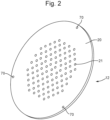
- the transmission plate 12 shown in Figure 2 comprises a regular array of circular apertures 21.
- the apertures 21 are arranged in a hexagonal array and are regularly spaced from one another across a central portion of the transmission plate 12.
- the lateral extent of the array could be chosen to match the maximum lateral dimension of substrates that can be accommodated by the substrate table 4, for example.
- the apertures 21 could alternatively be arranged in one or more concentric rings, for example.
- the circular disc 20 is manufactured from aluminium alloy no. 6082 with a thickness of between 4 to 10 millimetres.
- the diameter of the apertures 21 measured in the plane of the surface of the transmission plate 12 is preferably in the range of 0.5 to 1.5 times the thickness of the transmission plate 12.
- the diameter of the circular apertures is between 3 and 6 mm, with the diameter of all apertures preferably greater than 5 mm. An aperture diameter greater than 3 mm will begin to demonstrate favourable transmission characteristics.
- the transmission plate 12 is connected to the external chamber by three connecting points 70.
- apertures 21 and their sizes can be determined according to the desired electron distribution in the plasma cloud to impinge upon the wafer substrate 3 as is described in more detail in EP-A-1889946 subject to the constraints described below.
- the present invention is concerned with the recognition that the plasma also generates photons of light, particularly ultraviolet light, which can undesirably damage the wafer substrate 3.
- the invention particularly benefits processes intended to minimise residual damage to the substrate, such as atomic layer etching.
- the transmission plate 12 is designed to prevent there being a direct line of sight between the majority of the plasma 13, in particular the most intense region of the plasma 13, and the wafer substrate 3.
- the most intense region of the plasma 13 will be within the volume defined by the turns or segments of the coil 12.
- the apertures 21 each follow a non-rectilinear path through the transmission plate 12 such that there is no direct line of sight between the wafer substrate 3 and the most intense region of the plasma 13.
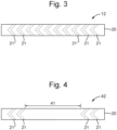
- FIG 3 shows a cross-sectional view of the transmission plate 12.
- the apertures 21 exhibit a change of direction as they pass through the plate (i.e. are non-rectilinear) so that there is no direct line of sight through the apertures from one side to the other.
- the apertures are each formed by two linear sections, which each extend into the transmission plate at an angle to the plane of the plate that is preferably in the range of 15 to 45 degrees. In this example the angle is about 20 degrees (and the two linear sections thus meet at about 40 degrees to one another inside the plate).
- apertures are provided across a central portion of the plate 12 as described above. This allows the transmission plate to be used for further control of the distribution of electrons across the wafer as described in more detail in EP-A-1889946 .
- apertures 21 could be omitted from a central portion 41 of the transmission plate 42 as shown in Figure 4 . In this latter example, the condition of preventing a direct line of sight with the most intense region of the plasma is further assured because the intensity of the plasma diminishes close to the wall of the plasma chamber.
- the line of sight condition can be achieved by configuring the apertures 21 such that there is no direct line of sight between the wafer 3 and a location on the plasma wall 8, indicated at 8A, nearest to the closest excitation point corresponding, in this case, to the lowest coil segment 7A of the RF coil 7.
- the design of the transmission plate 12 will define a maximum lateral dimension of the wafer substrate 3 so that wafers less than that maximum dimension (for example less than 100 mm) can all be used with the same transmission plate 12.
- the opaque central portion of the transmission plate may have a 200 mm diameter for use with a 100 mm wafer while in another example the opaque portion may have a 250 mm diameter for use with a wafer having a 200 mm diameter.
- the transmission plates described herein are suitable for use with the PlasmaPro 100 processing tool manufactured by Oxford Instruments, Bristol, UK.
- a plate 12 of this design reduces the ion flux to the substrate 3 by approximately a factor 10 compared to an unshielded source, but the ion flux can be restored by increasing the plasma power to the source.
- the plate and/or chamber walls or liners can be coated with an anti-reflective material (e.g. anodisation or similar) to minimise reflection of light.
- an anti-reflective material e.g. anodisation or similar
- the plate would typically be grounded, but could be powered by RF or DC to influence the transmission of ions.
- This configuration will not prevent all photons from reaching the wafer substrate 3 but will significantly attenuate exposure to light. In particular, it will significantly reduce light with photon energy of about 3 eV or higher which is capable of modifying chemical bonds and thereby damaging solid material.
- the plasma source power may be increased in order to compensate for any reduction in the flux of ions received at the substrate when the transmission plate is present (relative to the flux received when no transmission plate is provided). It is expected that the transmission plate will alter the ion velocity distribution function of ions inside the processing chamber in such a way as to reduce the electron temperature below the plate (again relative to when no transmission plate is provided). This reduces the production of high energy photons close to the substrate, and also reduces the minimum ion energy impacting on the substrate in the absence of additional bias energy at the table. Both of these are beneficial to an atomic layer etch process, by reducing photon damage to the remaining solid material, and improving control of low ion energy bombardment.
Landscapes
- Physics & Mathematics (AREA)
- Engineering & Computer Science (AREA)
- Plasma & Fusion (AREA)
- Chemical & Material Sciences (AREA)
- Analytical Chemistry (AREA)
- Electromagnetism (AREA)
- Spectroscopy & Molecular Physics (AREA)
- Drying Of Semiconductors (AREA)
- Plasma Technology (AREA)
Claims (14)
- Oberflächenbearbeitungseinrichtung zur Verwendung in der Oberflächenbearbeitung eines Substrats (3), wobei die Oberflächenbearbeitungseinrichtung umfasst:eine Plasmaquelle (1), die eine Wand, welche eine Plasmakammer (8) definiert, und eine an die Wand angrenzende Anregungsquelle beinhaltet;eine Bearbeitungskammer (2), in der ein Substrat (3), das eine vorbestimmte maximale seitliche Abmessung aufweist, im Gebrauch angebracht wird, wobei die Bearbeitungskammer (2) betriebsmäßig mit der Plasmaquelle (1) verbunden ist; undeine Übertragungsplatte (12) zur Übertragung von Plasma (13) im Gebrauch zwischen der Plasmaquelle (1) und der Bearbeitungskammer (2), wobei die Übertragungsplatte (12) eine Vielzahl von Öffnungen (21) umfasst, dadurch gekennzeichnet, dass die Öffnungen (21) einem nicht geradlinigen Pfad durch die Übertragungsplatte (12) folgen, derart, dass es im Gebrauch keine Sichtlinie zwischen einem Substrat (3) mit der vorbestimmten maximalen seitlichen Abmessung, das in der Bearbeitungskammer (2) angebracht ist, und dem intensivsten Bereich des Plasmas (13) in der Plasmakammer gibt, wobei die Öffnungen (21) kreisförmige Öffnungen sind und in einer regelmäßigen Anordnung angeordnet sind;wobei der intensivste Bereich des Plasmas (13) eine seitliche Begrenzung, die als der Teil der Plasmaquellenwand definiert ist, der an den Teil der Anregungsquelle angrenzt, der der Übertragungsplatte (12) am nächsten ist, und eine vertikale Begrenzung aufweist, die als die vertikale Position des Teils der Plasmaquellenwand definiert ist, der an den Teil der Anregungsquelle angrenzt, der der Übertragungsplatte (12) am nächsten ist.
- Einrichtung nach Anspruch 1, wobei ein zentraler Abschnitt der Übertragungsplatte (12) für Lichtwellenlängen von Interesse undurchlässig ist, wobei die seitliche Ausdehnung des undurchlässigen Abschnitts derart ist, dass es im Gebrauch keine Sichtlinie zwischen einem Substrat (3) mit der vorbestimmten maximalen seitlichen Abmessung, das in der Bearbeitungskammer angebracht ist, und dem intensivsten Bereich des Plasmas (13) in der Plasmakammer (8) gibt.
- Einrichtung nach Anspruch 1 oder 2, wobei die Übertragungsplatte (12) für Wellenlängen im ultravioletten Bereich undurchlässig ist.
- Einrichtung nach einem vorstehenden Anspruch, die exakt eine Übertragungsplatte (12) umfasst.
- Einrichtung nach einem vorstehenden Anspruch, wobei die Öffnungen (21) über mindestens einen zentralen Abschnitt der Übertragungsplatte (12), bevorzugt über im Wesentlichen die gesamte Übertragungsplatte (12), regelmäßig voneinander beabstandet sind.
- Oberflächenbearbeitungseinrichtung nach einem der vorstehenden Ansprüche, wobei die Plasmaquelle (1) ein induktiv gekoppeltes Plasma ist, bevorzugt wobei die Plasmaquelle (1) die Plasmakammer (8) und eine induktiv gekoppelte Spule (7) umfasst, besonders bevorzugt wobei die induktiv gekoppelte Spule (7) mit einer Hochfrequenz-(HF-) Quelle verbunden ist.
- Einrichtung nach Anspruch 6, wobei der Teil der Anregungsquelle, der der bzw. den Übertragungsplatte(n) (12) am nächsten ist, das Spulensegment (7A) der induktiv gekoppelten Spule (7) ist, das dem Substrat (3) am nächsten ist.
- Oberflächenbearbeitungseinrichtung nach einem der vorstehenden Ansprüche, wobei das Verhältnis von Öffnungsdurchmesser zu Übertragungsplattendicke im Bereich von 0,5:1 bis 1,5:1 liegt.
- Oberflächenbearbeitungseinrichtung nach einem der vorstehenden Ansprüche, wobei die Öffnungen (21) kreisförmig sind, wobei der Durchmesser jeder kreisförmigen Öffnung (21) größer als 3 mm, bevorzugt größer als 5 mm ist.
- Oberflächenbearbeitungseinrichtung nach einem der vorstehenden Ansprüche, wobei die Oberflächenbearbeitung des Substrats (3) das Entfernen von Material von der Oberfläche des Substrats (3) umfasst.
- Oberflächenbearbeitungseinrichtung nach einem der vorstehenden Ansprüche, wobei die thermische Leitfähigkeit der Übertragungsplatte (12) größer als 100 W m-1 K-1 ist.
- Oberflächenbearbeitungseinrichtung nach einem der vorstehenden Ansprüche, wobei die Übertragungsplatte (12) über einen Pfad mit geringem thermischem Widerstand thermisch mit der Bearbeitungskammer (2) verbunden ist.
- Oberflächenbearbeitungseinrichtung nach einem der vorstehenden Ansprüche, wobei die Übertragungsplatte (12) entweder (i) eine Metall- oder Metalllegierungsplatte, wobei die Metall- oder Legierungsplatte bevorzugt mit einer Lage beschichtet ist, die gegen Angriff durch das Plasma beständig ist, oder (ii) eine Keramikplatte, wie etwa eine Aluminiumoxidplatte, umfasst.
- Oberflächenbearbeitungseinrichtung nach einem der vorstehenden Ansprüche, die geeignet ist, um Atomlagenätzen durchzuführen.
Applications Claiming Priority (1)
| Application Number | Priority Date | Filing Date | Title |
|---|---|---|---|
| GBGB1904587.1A GB201904587D0 (en) | 2019-04-02 | 2019-04-02 | Surface processing apparatus |
Publications (2)
| Publication Number | Publication Date |
|---|---|
| EP3719833A1 EP3719833A1 (de) | 2020-10-07 |
| EP3719833B1 true EP3719833B1 (de) | 2023-09-13 |
Family
ID=66443037
Family Applications (1)
| Application Number | Title | Priority Date | Filing Date |
|---|---|---|---|
| EP20166698.9A Active EP3719833B1 (de) | 2019-04-02 | 2020-03-30 | Oberflächenverarbeitungsvorrichtung |
Country Status (4)
| Country | Link |
|---|---|
| US (1) | US11387075B2 (de) |
| EP (1) | EP3719833B1 (de) |
| FI (1) | FI3719833T3 (de) |
| GB (1) | GB201904587D0 (de) |
Families Citing this family (2)
| Publication number | Priority date | Publication date | Assignee | Title |
|---|---|---|---|---|
| JP6602887B2 (ja) * | 2015-03-19 | 2019-11-06 | マットソン テクノロジー インコーポレイテッド | プラズマ処理チャンバ内のエッチングプロセスのアジマス方向の均質性の制御 |
| AT528041B1 (de) * | 2024-02-21 | 2025-12-15 | Thermal Proc Solutions Gmbh | Einrichtung zur thermischen Behandlung eines Stoffes |
Family Cites Families (13)
| Publication number | Priority date | Publication date | Assignee | Title |
|---|---|---|---|---|
| JPH0831803A (ja) * | 1994-07-18 | 1996-02-02 | Plasma Syst:Kk | プラズマ処理装置 |
| JP3339200B2 (ja) * | 1994-09-28 | 2002-10-28 | ソニー株式会社 | プラズマ発生装置、プラズマ加工方法および薄膜トランジスタの製造方法 |
| US5968275A (en) | 1997-06-25 | 1999-10-19 | Lam Research Corporation | Methods and apparatus for passivating a substrate in a plasma reactor |
| US6083363A (en) | 1997-07-02 | 2000-07-04 | Tokyo Electron Limited | Apparatus and method for uniform, low-damage anisotropic plasma processing |
| US7591935B2 (en) * | 2005-12-14 | 2009-09-22 | Tokyo Electron Limited | Enhanced reliability deposition baffle for iPVD |
| GB0616131D0 (en) | 2006-08-14 | 2006-09-20 | Oxford Instr Plasma Technology | Surface processing apparatus |
| JP2009016453A (ja) | 2007-07-02 | 2009-01-22 | Tokyo Electron Ltd | プラズマ処理装置 |
| US9520275B2 (en) * | 2008-03-21 | 2016-12-13 | Tokyo Electron Limited | Mono-energetic neutral beam activated chemical processing system and method of using |
| JP5697389B2 (ja) * | 2010-09-27 | 2015-04-08 | 東京エレクトロン株式会社 | プラズマエッチング用の電極板及びプラズマエッチング処理装置 |
| JP5908001B2 (ja) * | 2014-01-16 | 2016-04-26 | 東京エレクトロン株式会社 | 基板処理装置 |
| KR101682155B1 (ko) * | 2015-04-20 | 2016-12-02 | 주식회사 유진테크 | 기판 처리 장치 |
| KR102227879B1 (ko) | 2016-01-15 | 2021-03-16 | 베이징 이타운 세미컨덕터 테크놀로지 컴퍼니 리미티드 | 플라즈마 챔버용 가변 패턴 분리 그리드 |
| US10790119B2 (en) * | 2017-06-09 | 2020-09-29 | Mattson Technology, Inc | Plasma processing apparatus with post plasma gas injection |
-
2019
- 2019-04-02 GB GBGB1904587.1A patent/GB201904587D0/en not_active Ceased
-
2020
- 2020-03-30 FI FIEP20166698.9T patent/FI3719833T3/fi active
- 2020-03-30 EP EP20166698.9A patent/EP3719833B1/de active Active
- 2020-04-01 US US16/837,262 patent/US11387075B2/en active Active
Also Published As
| Publication number | Publication date |
|---|---|
| US11387075B2 (en) | 2022-07-12 |
| GB201904587D0 (en) | 2019-05-15 |
| EP3719833A1 (de) | 2020-10-07 |
| US20200321192A1 (en) | 2020-10-08 |
| FI3719833T3 (fi) | 2023-10-04 |
Similar Documents
| Publication | Publication Date | Title |
|---|---|---|
| JP5546722B2 (ja) | 表面処理装置 | |
| US7837826B2 (en) | Hybrid RF capacitively and inductively coupled plasma source using multifrequency RF powers and methods of use thereof | |
| KR102411638B1 (ko) | 상류 플라즈마 소스들을 사용하는 챔버-후 저감 | |
| TWI851944B (zh) | 用於循環與選擇性材料移除與蝕刻的處理腔室 | |
| US6755150B2 (en) | Multi-core transformer plasma source | |
| US20180261429A1 (en) | Ion-ion plasma atomic layer etch process and reactor | |
| KR102311575B1 (ko) | 피처리체를 처리하는 방법 | |
| US20020033233A1 (en) | Icp reactor having a conically-shaped plasma-generating section | |
| US10032604B2 (en) | Remote plasma and electron beam generation system for a plasma reactor | |
| CN111247617A (zh) | 线性高能射频等离子体离子源 | |
| US20040007182A1 (en) | Plasma processing apparatus | |
| WO2020101838A1 (en) | Chamber seasoning to improve etch uniformity by reducing chemistry | |
| CN108140575A (zh) | 用于原子精度蚀刻的独立控制等离子体密度、自由基组成及离子能量的低电子温度蚀刻腔室 | |
| EP3719833B1 (de) | Oberflächenverarbeitungsvorrichtung | |
| CN100517553C (zh) | 用于膨胀热等离子体的电感耦合的系统和方法 | |
| JP4890550B2 (ja) | プラズマを発生させるための方法及び装置 | |
| JPH04291713A (ja) | プラズマcvd装置 |
Legal Events
| Date | Code | Title | Description |
|---|---|---|---|
| PUAI | Public reference made under article 153(3) epc to a published international application that has entered the european phase |
Free format text: ORIGINAL CODE: 0009012 |
|
| STAA | Information on the status of an ep patent application or granted ep patent |
Free format text: STATUS: THE APPLICATION HAS BEEN PUBLISHED |
|
| AK | Designated contracting states |
Kind code of ref document: A1 Designated state(s): AL AT BE BG CH CY CZ DE DK EE ES FI FR GB GR HR HU IE IS IT LI LT LU LV MC MK MT NL NO PL PT RO RS SE SI SK SM TR |
|
| AX | Request for extension of the european patent |
Extension state: BA ME |
|
| STAA | Information on the status of an ep patent application or granted ep patent |
Free format text: STATUS: REQUEST FOR EXAMINATION WAS MADE |
|
| 17P | Request for examination filed |
Effective date: 20210331 |
|
| RBV | Designated contracting states (corrected) |
Designated state(s): AL AT BE BG CH CY CZ DE DK EE ES FI FR GB GR HR HU IE IS IT LI LT LU LV MC MK MT NL NO PL PT RO RS SE SI SK SM TR |
|
| STAA | Information on the status of an ep patent application or granted ep patent |
Free format text: STATUS: EXAMINATION IS IN PROGRESS |
|
| 17Q | First examination report despatched |
Effective date: 20220202 |
|
| GRAP | Despatch of communication of intention to grant a patent |
Free format text: ORIGINAL CODE: EPIDOSNIGR1 |
|
| STAA | Information on the status of an ep patent application or granted ep patent |
Free format text: STATUS: GRANT OF PATENT IS INTENDED |
|
| INTG | Intention to grant announced |
Effective date: 20230413 |
|
| P01 | Opt-out of the competence of the unified patent court (upc) registered |
Effective date: 20230516 |
|
| GRAS | Grant fee paid |
Free format text: ORIGINAL CODE: EPIDOSNIGR3 |
|
| GRAA | (expected) grant |
Free format text: ORIGINAL CODE: 0009210 |
|
| STAA | Information on the status of an ep patent application or granted ep patent |
Free format text: STATUS: THE PATENT HAS BEEN GRANTED |
|
| AK | Designated contracting states |
Kind code of ref document: B1 Designated state(s): AL AT BE BG CH CY CZ DE DK EE ES FI FR GB GR HR HU IE IS IT LI LT LU LV MC MK MT NL NO PL PT RO RS SE SI SK SM TR |
|
| REG | Reference to a national code |
Ref country code: CH Ref legal event code: EP |
|
| REG | Reference to a national code |
Ref country code: FI Ref legal event code: FGE |
|
| REG | Reference to a national code |
Ref country code: DE Ref legal event code: R096 Ref document number: 602020017491 Country of ref document: DE |
|
| REG | Reference to a national code |
Ref country code: IE Ref legal event code: FG4D |
|
| REG | Reference to a national code |
Ref country code: NL Ref legal event code: FP |
|
| REG | Reference to a national code |
Ref country code: LT Ref legal event code: MG9D |
|
| PG25 | Lapsed in a contracting state [announced via postgrant information from national office to epo] |
Ref country code: GR Free format text: LAPSE BECAUSE OF FAILURE TO SUBMIT A TRANSLATION OF THE DESCRIPTION OR TO PAY THE FEE WITHIN THE PRESCRIBED TIME-LIMIT Effective date: 20231214 |
|
| PG25 | Lapsed in a contracting state [announced via postgrant information from national office to epo] |
Ref country code: SE Free format text: LAPSE BECAUSE OF FAILURE TO SUBMIT A TRANSLATION OF THE DESCRIPTION OR TO PAY THE FEE WITHIN THE PRESCRIBED TIME-LIMIT Effective date: 20230913 Ref country code: RS Free format text: LAPSE BECAUSE OF FAILURE TO SUBMIT A TRANSLATION OF THE DESCRIPTION OR TO PAY THE FEE WITHIN THE PRESCRIBED TIME-LIMIT Effective date: 20230913 Ref country code: NO Free format text: LAPSE BECAUSE OF FAILURE TO SUBMIT A TRANSLATION OF THE DESCRIPTION OR TO PAY THE FEE WITHIN THE PRESCRIBED TIME-LIMIT Effective date: 20231213 Ref country code: LV Free format text: LAPSE BECAUSE OF FAILURE TO SUBMIT A TRANSLATION OF THE DESCRIPTION OR TO PAY THE FEE WITHIN THE PRESCRIBED TIME-LIMIT Effective date: 20230913 Ref country code: LT Free format text: LAPSE BECAUSE OF FAILURE TO SUBMIT A TRANSLATION OF THE DESCRIPTION OR TO PAY THE FEE WITHIN THE PRESCRIBED TIME-LIMIT Effective date: 20230913 Ref country code: HR Free format text: LAPSE BECAUSE OF FAILURE TO SUBMIT A TRANSLATION OF THE DESCRIPTION OR TO PAY THE FEE WITHIN THE PRESCRIBED TIME-LIMIT Effective date: 20230913 Ref country code: GR Free format text: LAPSE BECAUSE OF FAILURE TO SUBMIT A TRANSLATION OF THE DESCRIPTION OR TO PAY THE FEE WITHIN THE PRESCRIBED TIME-LIMIT Effective date: 20231214 |
|
| REG | Reference to a national code |
Ref country code: AT Ref legal event code: MK05 Ref document number: 1612177 Country of ref document: AT Kind code of ref document: T Effective date: 20230913 |
|
| PG25 | Lapsed in a contracting state [announced via postgrant information from national office to epo] |
Ref country code: IS Free format text: LAPSE BECAUSE OF FAILURE TO SUBMIT A TRANSLATION OF THE DESCRIPTION OR TO PAY THE FEE WITHIN THE PRESCRIBED TIME-LIMIT Effective date: 20240113 |
|
| PG25 | Lapsed in a contracting state [announced via postgrant information from national office to epo] |
Ref country code: AT Free format text: LAPSE BECAUSE OF FAILURE TO SUBMIT A TRANSLATION OF THE DESCRIPTION OR TO PAY THE FEE WITHIN THE PRESCRIBED TIME-LIMIT Effective date: 20230913 |
|
| PG25 | Lapsed in a contracting state [announced via postgrant information from national office to epo] |
Ref country code: ES Free format text: LAPSE BECAUSE OF FAILURE TO SUBMIT A TRANSLATION OF THE DESCRIPTION OR TO PAY THE FEE WITHIN THE PRESCRIBED TIME-LIMIT Effective date: 20230913 |
|
| PG25 | Lapsed in a contracting state [announced via postgrant information from national office to epo] |
Ref country code: SM Free format text: LAPSE BECAUSE OF FAILURE TO SUBMIT A TRANSLATION OF THE DESCRIPTION OR TO PAY THE FEE WITHIN THE PRESCRIBED TIME-LIMIT Effective date: 20230913 Ref country code: RO Free format text: LAPSE BECAUSE OF FAILURE TO SUBMIT A TRANSLATION OF THE DESCRIPTION OR TO PAY THE FEE WITHIN THE PRESCRIBED TIME-LIMIT Effective date: 20230913 Ref country code: IS Free format text: LAPSE BECAUSE OF FAILURE TO SUBMIT A TRANSLATION OF THE DESCRIPTION OR TO PAY THE FEE WITHIN THE PRESCRIBED TIME-LIMIT Effective date: 20240113 Ref country code: ES Free format text: LAPSE BECAUSE OF FAILURE TO SUBMIT A TRANSLATION OF THE DESCRIPTION OR TO PAY THE FEE WITHIN THE PRESCRIBED TIME-LIMIT Effective date: 20230913 Ref country code: EE Free format text: LAPSE BECAUSE OF FAILURE TO SUBMIT A TRANSLATION OF THE DESCRIPTION OR TO PAY THE FEE WITHIN THE PRESCRIBED TIME-LIMIT Effective date: 20230913 Ref country code: CZ Free format text: LAPSE BECAUSE OF FAILURE TO SUBMIT A TRANSLATION OF THE DESCRIPTION OR TO PAY THE FEE WITHIN THE PRESCRIBED TIME-LIMIT Effective date: 20230913 Ref country code: AT Free format text: LAPSE BECAUSE OF FAILURE TO SUBMIT A TRANSLATION OF THE DESCRIPTION OR TO PAY THE FEE WITHIN THE PRESCRIBED TIME-LIMIT Effective date: 20230913 Ref country code: SK Free format text: LAPSE BECAUSE OF FAILURE TO SUBMIT A TRANSLATION OF THE DESCRIPTION OR TO PAY THE FEE WITHIN THE PRESCRIBED TIME-LIMIT Effective date: 20230913 Ref country code: PT Free format text: LAPSE BECAUSE OF FAILURE TO SUBMIT A TRANSLATION OF THE DESCRIPTION OR TO PAY THE FEE WITHIN THE PRESCRIBED TIME-LIMIT Effective date: 20240115 |
|
| PG25 | Lapsed in a contracting state [announced via postgrant information from national office to epo] |
Ref country code: PL Free format text: LAPSE BECAUSE OF FAILURE TO SUBMIT A TRANSLATION OF THE DESCRIPTION OR TO PAY THE FEE WITHIN THE PRESCRIBED TIME-LIMIT Effective date: 20230913 Ref country code: IT Free format text: LAPSE BECAUSE OF FAILURE TO SUBMIT A TRANSLATION OF THE DESCRIPTION OR TO PAY THE FEE WITHIN THE PRESCRIBED TIME-LIMIT Effective date: 20230913 |
|
| REG | Reference to a national code |
Ref country code: DE Ref legal event code: R097 Ref document number: 602020017491 Country of ref document: DE |
|
| PG25 | Lapsed in a contracting state [announced via postgrant information from national office to epo] |
Ref country code: DK Free format text: LAPSE BECAUSE OF FAILURE TO SUBMIT A TRANSLATION OF THE DESCRIPTION OR TO PAY THE FEE WITHIN THE PRESCRIBED TIME-LIMIT Effective date: 20230913 |
|
| PLBE | No opposition filed within time limit |
Free format text: ORIGINAL CODE: 0009261 |
|
| STAA | Information on the status of an ep patent application or granted ep patent |
Free format text: STATUS: NO OPPOSITION FILED WITHIN TIME LIMIT |
|
| PG25 | Lapsed in a contracting state [announced via postgrant information from national office to epo] |
Ref country code: DK Free format text: LAPSE BECAUSE OF FAILURE TO SUBMIT A TRANSLATION OF THE DESCRIPTION OR TO PAY THE FEE WITHIN THE PRESCRIBED TIME-LIMIT Effective date: 20230913 |
|
| 26N | No opposition filed |
Effective date: 20240614 |
|
| PG25 | Lapsed in a contracting state [announced via postgrant information from national office to epo] |
Ref country code: SI Free format text: LAPSE BECAUSE OF FAILURE TO SUBMIT A TRANSLATION OF THE DESCRIPTION OR TO PAY THE FEE WITHIN THE PRESCRIBED TIME-LIMIT Effective date: 20230913 |
|
| PG25 | Lapsed in a contracting state [announced via postgrant information from national office to epo] |
Ref country code: SI Free format text: LAPSE BECAUSE OF FAILURE TO SUBMIT A TRANSLATION OF THE DESCRIPTION OR TO PAY THE FEE WITHIN THE PRESCRIBED TIME-LIMIT Effective date: 20230913 |
|
| REG | Reference to a national code |
Ref country code: CH Ref legal event code: PL |
|
| PG25 | Lapsed in a contracting state [announced via postgrant information from national office to epo] |
Ref country code: BG Free format text: LAPSE BECAUSE OF FAILURE TO SUBMIT A TRANSLATION OF THE DESCRIPTION OR TO PAY THE FEE WITHIN THE PRESCRIBED TIME-LIMIT Effective date: 20230913 |
|
| PG25 | Lapsed in a contracting state [announced via postgrant information from national office to epo] |
Ref country code: LU Free format text: LAPSE BECAUSE OF NON-PAYMENT OF DUE FEES Effective date: 20240330 |
|
| PG25 | Lapsed in a contracting state [announced via postgrant information from national office to epo] |
Ref country code: MC Free format text: LAPSE BECAUSE OF FAILURE TO SUBMIT A TRANSLATION OF THE DESCRIPTION OR TO PAY THE FEE WITHIN THE PRESCRIBED TIME-LIMIT Effective date: 20230913 |
|
| PG25 | Lapsed in a contracting state [announced via postgrant information from national office to epo] |
Ref country code: MC Free format text: LAPSE BECAUSE OF FAILURE TO SUBMIT A TRANSLATION OF THE DESCRIPTION OR TO PAY THE FEE WITHIN THE PRESCRIBED TIME-LIMIT Effective date: 20230913 Ref country code: LU Free format text: LAPSE BECAUSE OF NON-PAYMENT OF DUE FEES Effective date: 20240330 Ref country code: BG Free format text: LAPSE BECAUSE OF FAILURE TO SUBMIT A TRANSLATION OF THE DESCRIPTION OR TO PAY THE FEE WITHIN THE PRESCRIBED TIME-LIMIT Effective date: 20230913 |
|
| REG | Reference to a national code |
Ref country code: BE Ref legal event code: MM Effective date: 20240331 |
|
| PG25 | Lapsed in a contracting state [announced via postgrant information from national office to epo] |
Ref country code: BE Free format text: LAPSE BECAUSE OF NON-PAYMENT OF DUE FEES Effective date: 20240331 |
|
| PG25 | Lapsed in a contracting state [announced via postgrant information from national office to epo] |
Ref country code: FR Free format text: LAPSE BECAUSE OF NON-PAYMENT OF DUE FEES Effective date: 20240331 |
|
| PG25 | Lapsed in a contracting state [announced via postgrant information from national office to epo] |
Ref country code: IE Free format text: LAPSE BECAUSE OF NON-PAYMENT OF DUE FEES Effective date: 20240330 |
|
| PG25 | Lapsed in a contracting state [announced via postgrant information from national office to epo] |
Ref country code: IE Free format text: LAPSE BECAUSE OF NON-PAYMENT OF DUE FEES Effective date: 20240330 Ref country code: FR Free format text: LAPSE BECAUSE OF NON-PAYMENT OF DUE FEES Effective date: 20240331 Ref country code: BE Free format text: LAPSE BECAUSE OF NON-PAYMENT OF DUE FEES Effective date: 20240331 Ref country code: CH Free format text: LAPSE BECAUSE OF NON-PAYMENT OF DUE FEES Effective date: 20240331 |
|
| PG25 | Lapsed in a contracting state [announced via postgrant information from national office to epo] |
Ref country code: CY Free format text: LAPSE BECAUSE OF FAILURE TO SUBMIT A TRANSLATION OF THE DESCRIPTION OR TO PAY THE FEE WITHIN THE PRESCRIBED TIME-LIMIT; INVALID AB INITIO Effective date: 20200330 |
|
| PG25 | Lapsed in a contracting state [announced via postgrant information from national office to epo] |
Ref country code: HU Free format text: LAPSE BECAUSE OF FAILURE TO SUBMIT A TRANSLATION OF THE DESCRIPTION OR TO PAY THE FEE WITHIN THE PRESCRIBED TIME-LIMIT; INVALID AB INITIO Effective date: 20200330 |
|
| PG25 | Lapsed in a contracting state [announced via postgrant information from national office to epo] |
Ref country code: TR Free format text: LAPSE BECAUSE OF FAILURE TO SUBMIT A TRANSLATION OF THE DESCRIPTION OR TO PAY THE FEE WITHIN THE PRESCRIBED TIME-LIMIT Effective date: 20230913 |
|
| REG | Reference to a national code |
Ref country code: DE Ref legal event code: R081 Ref document number: 602020017491 Country of ref document: DE Owner name: OXFORD INSTRUMENTS NANOTECHNOLOGY TOOLS LIMITE, GB Free format text: FORMER OWNER: OXFORD INSTRUMENTS NANOTECHNOLOGY TOOLS LIMITED, ABINGDON, OXON, GB |
|
| PGFP | Annual fee paid to national office [announced via postgrant information from national office to epo] |
Ref country code: NL Payment date: 20260227 Year of fee payment: 7 |
|
| PGFP | Annual fee paid to national office [announced via postgrant information from national office to epo] |
Ref country code: GB Payment date: 20260223 Year of fee payment: 7 |
|
| PGFP | Annual fee paid to national office [announced via postgrant information from national office to epo] |
Ref country code: DE Payment date: 20260218 Year of fee payment: 7 |
|
| PGFP | Annual fee paid to national office [announced via postgrant information from national office to epo] |
Ref country code: FI Payment date: 20260312 Year of fee payment: 7 |