EP3719994B1 - Régulation de puissance d'éclairage utilisant des communications de champ proche - Google Patents
Régulation de puissance d'éclairage utilisant des communications de champ proche Download PDFInfo
- Publication number
- EP3719994B1 EP3719994B1 EP19166553.8A EP19166553A EP3719994B1 EP 3719994 B1 EP3719994 B1 EP 3719994B1 EP 19166553 A EP19166553 A EP 19166553A EP 3719994 B1 EP3719994 B1 EP 3719994B1
- Authority
- EP
- European Patent Office
- Prior art keywords
- circuit
- nfc
- signal
- mode
- supply voltage
- Prior art date
- Legal status (The legal status is an assumption and is not a legal conclusion. Google has not performed a legal analysis and makes no representation as to the accuracy of the status listed.)
- Active
Links
Images

Classifications
-
- H—ELECTRICITY
- H03—ELECTRONIC CIRCUITRY
- H03K—PULSE TECHNIQUE
- H03K7/00—Modulating pulses with a continuously-variable modulating signal
- H03K7/08—Duration or width modulation ; Duty cycle modulation
-
- H—ELECTRICITY
- H05—ELECTRIC TECHNIQUES NOT OTHERWISE PROVIDED FOR
- H05B—ELECTRIC HEATING; ELECTRIC LIGHT SOURCES NOT OTHERWISE PROVIDED FOR; CIRCUIT ARRANGEMENTS FOR ELECTRIC LIGHT SOURCES, IN GENERAL
- H05B45/00—Circuit arrangements for operating light-emitting diodes [LED]
- H05B45/30—Driver circuits
- H05B45/32—Pulse-control circuits
- H05B45/325—Pulse-width modulation [PWM]
-
- H—ELECTRICITY
- H02—GENERATION; CONVERSION OR DISTRIBUTION OF ELECTRIC POWER
- H02J—ELECTRIC POWER NETWORKS; CIRCUIT ARRANGEMENTS OR SYSTEMS FOR SUPPLYING OR DISTRIBUTING ELECTRIC POWER; SYSTEMS FOR STORING ELECTRIC ENERGY
- H02J50/00—Circuit arrangements or systems for wireless supply or distribution of electric power
- H02J50/80—Circuit arrangements or systems for wireless supply or distribution of electric power involving the exchange of data, concerning supply or distribution of electric power, between transmitting devices and receiving devices
-
- H—ELECTRICITY
- H04—ELECTRIC COMMUNICATION TECHNIQUE
- H04B—TRANSMISSION
- H04B5/00—Near-field transmission systems, e.g. inductive or capacitive transmission systems
- H04B5/20—Near-field transmission systems, e.g. inductive or capacitive transmission systems characterised by the transmission technique; characterised by the transmission medium
-
- H—ELECTRICITY
- H04—ELECTRIC COMMUNICATION TECHNIQUE
- H04B—TRANSMISSION
- H04B5/00—Near-field transmission systems, e.g. inductive or capacitive transmission systems
- H04B5/20—Near-field transmission systems, e.g. inductive or capacitive transmission systems characterised by the transmission technique; characterised by the transmission medium
- H04B5/24—Inductive coupling
-
- H—ELECTRICITY
- H04—ELECTRIC COMMUNICATION TECHNIQUE
- H04B—TRANSMISSION
- H04B5/00—Near-field transmission systems, e.g. inductive or capacitive transmission systems
- H04B5/20—Near-field transmission systems, e.g. inductive or capacitive transmission systems characterised by the transmission technique; characterised by the transmission medium
- H04B5/24—Inductive coupling
- H04B5/26—Inductive coupling using coils
-
- H—ELECTRICITY
- H04—ELECTRIC COMMUNICATION TECHNIQUE
- H04B—TRANSMISSION
- H04B5/00—Near-field transmission systems, e.g. inductive or capacitive transmission systems
- H04B5/70—Near-field transmission systems, e.g. inductive or capacitive transmission systems specially adapted for specific purposes
- H04B5/79—Near-field transmission systems, e.g. inductive or capacitive transmission systems specially adapted for specific purposes for data transfer in combination with power transfer
-
- H—ELECTRICITY
- H04—ELECTRIC COMMUNICATION TECHNIQUE
- H04W—WIRELESS COMMUNICATION NETWORKS
- H04W52/00—Power management, e.g. Transmission Power Control [TPC] or power classes
- H04W52/02—Power saving arrangements
-
- H—ELECTRICITY
- H05—ELECTRIC TECHNIQUES NOT OTHERWISE PROVIDED FOR
- H05B—ELECTRIC HEATING; ELECTRIC LIGHT SOURCES NOT OTHERWISE PROVIDED FOR; CIRCUIT ARRANGEMENTS FOR ELECTRIC LIGHT SOURCES, IN GENERAL
- H05B45/00—Circuit arrangements for operating light-emitting diodes [LED]
- H05B45/20—Controlling the colour of the light
- H05B45/24—Controlling the colour of the light using electrical feedback from LEDs or from LED modules
-
- H—ELECTRICITY
- H05—ELECTRIC TECHNIQUES NOT OTHERWISE PROVIDED FOR
- H05B—ELECTRIC HEATING; ELECTRIC LIGHT SOURCES NOT OTHERWISE PROVIDED FOR; CIRCUIT ARRANGEMENTS FOR ELECTRIC LIGHT SOURCES, IN GENERAL
- H05B45/00—Circuit arrangements for operating light-emitting diodes [LED]
- H05B45/30—Driver circuits
-
- H—ELECTRICITY
- H04—ELECTRIC COMMUNICATION TECHNIQUE
- H04B—TRANSMISSION
- H04B5/00—Near-field transmission systems, e.g. inductive or capacitive transmission systems
- H04B5/70—Near-field transmission systems, e.g. inductive or capacitive transmission systems specially adapted for specific purposes
Definitions
- the present disclosure relates to controllers for use in lighting applications, particularly in lighting applications using LED devices.
- LEDs Light Emitting Diodes
- the load current control is usually implemented using dedicated LED driver circuits which may be configured to regulate the load current passing through a LED module (usually a series circuit of a plurality of LEDs) to match a given set-point.
- the set-point may be configurable. For example, the set-point may be set in accordance with an analog input voltage, which represents the information about the desired set-point (and thus about the desired output power). In low-cost applications, the set-point may be set using a resistor supplied with a constant current so that the voltage that determines the set-point is substantially proportional to the resistance of the resistor. In some applications DIP switches are used to select resistors of a resistor network, thereby adjusting the effective resistance of the resistor network which determines the mentioned set-point.
- a power limitation may be included in the LED driver circuit to ensure that the electrical power provided to the LED device does not exceed a maximum value. Similarly, the electrical power provided to the LED device should not fall below a minimum value.
- These power limits may also be configurable in order to comply with the requirements of a specific application. In some applications simple but expensive discrete analog circuitry is used to implement the above-mentioned power limitation.
- a microcontroller may be used in connection with a LED driver circuit, wherein the microcontroller may be programmed to sense voltage and load current (using an analog-to-digital converter) and to control the above-mentioned set-point in order to operate the LED device within specified limits.
- the application-dependent and customer-dependent configuration parameters e.g. nominal current set-point, power limit, etc.
- the publication DE 10 2015 105 466 A1 relates to a driver circuit for LED devices used in illumination products.
- the driver circuit includes a wireless interface for receiving information relating to the operation of the illumination product.
- the publication WO 2016/081244 A1 relates to a medical device which can be activated by bringing an NFC enabled mobile device into close proximity of the medical device, thus making a dedicated witch dispensable.
- the publication US 2013/0234658 A1 relates to a wireless charging circuit.
- a circuit comprises a supply pin configured to receive a supply voltage, a non-volatile memory for storing one or more parameters, and a Near Field Communication (NFC) transceiver that is configured to receive data representing the one or more parameters in a second mode of operation, in which no supply voltage is received at the supply pin .
- the circuit is configured in a first mode of operation to deactivate the NFC transceiver in response to receiving the supply voltage at the supply pin
- the circuit comprises a modulator configured to generate, in the first mode of operation, a modulated output signal, which depends on at least one of the one or more parameters stored in the non-volatile memory.
- a method for operating a circuit which comprises a supply pin, a non-volatile memory, and a NFC transceiver, is described herein according to the invention.
- the method comprises - in a second mode of operation, in which no supply voltage is received at the supply pin - receiving, by the NFC transceiver, data representing one or more parameters and storing the one or more parameters in the non-volatile memory, and - in a first mode of operation, in which the supply voltage is received at the supply pin - deactivating the NFC transceiver
- the method further comprises, in the first mode of operation, generating a modulated output signal dependent on at least one of the one or more parameters stored in the non-volatile memory
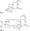
- Fig. 1 illustrates a generic example of a system including a LED device 20, which is usually composed of a series circuit of a plurality of LEDs (LED chain), and a LED driver circuit 10, to which the LED chain is connected.
- the LED driver circuit 20 may be implemented in one integrated circuit but may also be implemented using a combination of discrete circuit components and integrated circuits.
- the LED driver circuit 10 is configured to provide a load current iour to the LED device 20 and to control the load current i OUT so that its current value (at least approximately) matches a set-point (desired current value). It is understood that the system of Fig. 1 or similar systems may be used, for example, to produce a lighting module that includes the LED device 20 and all circuitry required to drive the LED device 20.
- the LED device 20 is connected between an output terminal OUT of the LED driver circuit 10 and a supply terminal PWR, to which an input voltage V IN is applied.
- the input voltage V EST may also be received at the terminal VIN of the LED driver circuit 10.
- the LED driver circuit 10 is connected to a ground terminal GND.
- the input voltage V IN may vary within a comparably wide range. In the present example, the input voltage may vary between 25 and 40 volts. However, this range may be different in other applications.
- the LED driver circuit 10 may be configured to operate the LED device 20 so that the electrical power (load current times input voltage) does not exceed a specific maximum power. In some applications the electrical power should not fall below a specific minimum power.
- the set-point is determined by the voltage V SET received at analog input terminal SET.
- the voltage V SET may be applied either using an external voltage source or by connecting a resistor R SET between the analog input terminal SET and, e.g., ground terminal GND.
- the current set-point used for the regulation of the load current may be proportional to the voltage V SET .
- a microcontroller may use analog-to-digital converters (included in common standard microcontrollers) to obtain measured values representing the input voltage V IN and the load current i OUT , wherein a digital-to-analog converter may be used to generate the desired voltage V SET , which may be adjusted, for example, dependent on an electrical power value calculated by the microcontroller based on the above-mentioned measured values.
- NVM non-volatile memory
- ISP wired in-system programming
- Fig. 2 illustrates a novel approach which may significantly improve flexibility while keeping the bill of materials and production costs low.
- the example of Fig. 2 includes a control circuit 5, an LED driver circuit 10 as well as an LED device 10 connected thereto.
- the LED driver circuit 10 and the LED device 20 are substantially the same as in the previous example of Fig. 1 and reference is made to the respective description above.
- a current sense resistor Rs is coupled in series to the LED device 20 in order to allow measurement of the load current.
- the resistor Rs is connected between the LED device 20 and the terminal PWR, at which the input voltage V EST is provided.
- the shunt resistor or other current sense circuitry may be integrated in the LED device 20 and the current information can be tapped at a dedicated sense terminal of the LED device 20.
- the control circuit 5 is configured to provide, at output terminal DOUT (digital output), an output voltage V PWM that is indicative of the set-point, which is used by the LED driver circuit for the purpose of output current regulation.
- the output voltage V PWM is a pulse-width modulated (PWM) signal that is converted to an analog voltage V SET using, for example, a low pass.
- PWM pulse-width modulated
- a simple R-C low-pass composed of one resistor R 1 and one capacitor C 1 may be sufficient to generate the voltage V SET from the PWM signal.
- the resistor R 1 and the capacitor C 1 may be integrated into the control circuit 5 or connected externally to an integrated circuit (IC).
- pulse-width modulation is merely one example and other types of modulation, such as sigma-delta modulation, may be employed instead.
- the low-pass may be regarded as an digital-to-analog converter that is configured to convert the (binary) PWM signal into the analog voltage V SET . It is understood that other approaches for digital-to-analog conversion may be used instead.
- the control circuit 5 has two analog inputs AIN1 and AIN2, which receive the input voltage V EST and the voltage Vs at the common circuit node of shunt resistor Rs and LED device 20.
- the voltage Vs equals V IN -R S ⁇ i OUT
- the control circuit 5 may include an analog-to-digital converter to digitize the voltages V IN and Vs; in this case the control circuit 5 can regularly digitally calculate the load current value and adjust the set-point in accordance with a given control characteristic.
- the set-point information is output as the PWM signal V PWM .
- the control circuit may include a Near Field Communication (NFC) transceiver circuit as well as an NFC antenna 4 connected thereto.
- NFC Near Field Communication
- the nominal set-point and other parameters can be easily programmed using an NFC coupling device (e.g. an NFC writer) that is configured to transmit the information about the parameters to the NFC transceiver circuit included in the control circuit 5, which then stores the received information, e.g., in a non-volatile memory (NVM) that may be integrated in the control circuit 5.
- NFC coupling device e.g. an NFC writer
- NVM non-volatile memory
- Fig. 3 illustrates one exemplary embodiment of the control circuit 5 used in the example of Fig. 2 .
- the control circuit 5 may be implemented in one single integrated circuit, e.g. an application specific integrated circuit (ASIC).
- the control circuit 5 includes a power management unit 50 (PMU), one or more analog-to-digital converters 52, the above-mentioned NFC transceiver 53, as well as a control logic 51, which basically forms a finite state machine (FSM).
- the control circuit 5 further includes an NVM 54, an arithmetic-logic unit 56 (ALU) and a modulator 55 configured to generate the PWM output signal V PMW (see Fig. 2 ).
- PMU power management unit 50
- ALU arithmetic-logic unit 56
- modulator 55 configured to generate the PWM output signal V PMW (see Fig. 2 ).
- An oscillator 57 generates a clock signal for the logic circuit 51, the ALU 56, the modulator 55 and further circuitry that need the clock signal for operation.
- the ALU 56 can be regarded as part of the logic circuit 51 which is, however, an implementation detail irrelevant for the function of the overall control circuit 5.
- the power management unit 50 receives, at respective supply pins, a first supply voltage Vcc (e.g. 5 volts) and a reference potential V GND , e.g. ground potential.
- Vcc a first supply voltage
- V GND a reference potential
- the PMU may receive a supply voltage V NFC from the NFC transceiver 53 when the NFC transceiver 53 receives energy from an external NFC coupling device (not shown) via NFC antenna 4.
- the NFC transceiver 53 and its functions will be discussed in more detail later.
- the PMU 50 is configured to provide voltage supply to all circuitry included in the control circuit 5.
- the analog-to-digital converter (ADC) 52 receives, at respective analog input pins (see Fig. 2 , terminals AIN1, AIN2), voltage signals V EST and Vs which carry information about the input voltage V IN and the load current i OUT passing through the LED device 20.
- ADC may have two channels that are able to simultaneously sample the voltage signals V IN and Vs or a multiplexer may be used to use one ADC channel for sampling both signals V IN and Vs in an alternating manner.
- the control logic 51 is configured to control the operation of the control circuit 5 and particularly the signal flow within the control circuit 5.
- the NVM 54 and the ALU 56 are connected to the control logic 51, which is configured to determine (with the help of the ALU 56) the set-point to be used for current regulation based on the parameters (e.g. the nominal set-point value) stored in the NVM 54 and the sampled values received from the ADC 52.
- the control logic 51 is further configured to provide the set-point information (e.g. in the form of a digital word) to the modulator 55.
- the modulator 55 is configured to output, e.g. at a digital output pin DOUT, a PWM signal V OUT which has a duty cycle that represents the set-point information.
- the control logic 51 will reduce the set-point accordingly and, consequently, the PWM signal output to the LED driver circuit 10 will indicate a lower set-point and the current regulator included in the LED driver circuit 10 will reduce the load current.
- the modulator 55 is not necessarily configured to perform pulse-width modulation (PWM), and other types of modulation such as, for example, sigma-delta modulation (pulse density modulation) are also applicable.
- parameters such as a nominal current set-point can be received by the NFC transceiver 53 from an external NFC coupling device (not shown in the figures) and stored in the NVM 54.
- the control circuit 5, and particularly the control logic 51 included therein is configured to operate in two different modes.
- the first mode which may be referred to as programming mode, is characterized in that the control circuit 5 is not supplied with the supply voltage Vcc at the respective supply pin but rather receives electrical power from an active NFC field generated by an external NFC device.
- the NFC transceiver will generate a supply voltage V NFC which can be distributed to the control logic 51 and the NVM 54 (e.g.
- the second mode which may be referred to as normal mode of operation, is characterized in that the control circuit 5 is supplied with the supply voltage Vcc at the respective supply pin.
- the NFC transceiver is disabled, e.g. by receiving a respective mode signal (disable signal) from the PMU 50 in response to the PMU 50 detecting the presence of the supply voltage VCC at the supply pin.
- the disable signal may be generated by the control logic 51 or other circuitry included in the control circuit 5.
- the NFC transceiver 53 being disabled means that the NFC transceiver 53 can neither generate an NFC field nor transmit any RF signals via the antenna 4.
- an electronic switch may be used to prevent the NFC transceiver 53 from generating the supply voltage V NFC from an externally generated (e.g. by an NFC coupling device) NFC field.
- the electronic switch e.g. a depletion MOS transistor
- the electronic switch may for example disconnect or short circuit a capacitor, which is used to buffer the voltage V NFC when the supply voltage Vcc is present at the respective supply pin.
- an electronic switch may be used, for example, to disconnect the NFC antenna 4 or otherwise disable the NFC antenna 4 (e.g. by short-circuiting the two antenna terminals using an electronic switch).
- the NFC transceiver 53 may be permanently deactivated once a parameter set has been successfully received via the NFC communication channel and stored in the NVM 54.
- This permanent deactivation may be achieved in various ways.
- the NFC transceiver may include an electrically programmable fuse bit which is set once a parameter set has been successfully received and stored. Based on the state of the fuse bit, the NFC transceiver 53 may be deactivated in a similar manner as described above.
- control logic 51 as well as the ALU 56 (which may also be regarded as part of the control logic 51) are composed of hard-wired circuit components and do not require software. In other words, the control logic 51 does not include a processor configured to execute software instructions. Furthermore, the control circuit 51, the PMU 50, the ADC 52 as well as the NFC transceiver 53 are integrated in a single chip or a single chip package. Integration in a common chip allows for a comparably simple deactivation of the NFC transceiver 53 when the supply voltage Vcc is received at the respective supply pin normal mode of operation).
- Fig. 4 is a flow chart illustrating a method in accordance with the invention. The method may be essentially (but not exclusively) performed by the control logic 51 of the control circuit 5 described above. According to Fig. 4 the circuit is able to operate in a first mode or a second mode. The circuit operates in the first mode, when a supply voltage Vcc is received at the supply pin ( Fig. 4 , step S1, yes-branch). The circuit operates in the second mode, when no supply voltage Vcc is received at the supply pin ( Fig. 4 , step S1, no-branch) and when an NFC field is present so that the NFC transceiver is able to generate an alternative supply voltage V NFC from the NFC field ( Fig. 4 , step S2, yes-branch).
- the circuit is passive and does not operate.
- the NFC transceiver is deactivated ( Fig. 4 , step S11). Further functions provided in the first mode (e.g. generating modulated signal V PWM , etc.) have been discussed above and not repeated here.
- the NFC field is the only source of energy of the circuit, and the NFC transceiver generates the alternative supply voltage V NFC for supplying other circuitry such as the control logic 51 and the NVM 54 (cf. Fig.
- the NFC communication channel Fig 4 , step S21
- the received data i.e. the one or more parameters discussed above, e.g. a nominal current set-point to be used for current regulation
- the NVM 54 Fig 4 , step S22
- operation in the second mode can only start when the fuse bit state indicates that the NVM 54 has not yet been programmed. Once the fuse bit has been fused (set) the NFC transceiver 53 is prevented from generating the alternative supply voltage V NFC from an external NFC field, and thus the circuit does not power up.
Landscapes
- Engineering & Computer Science (AREA)
- Computer Networks & Wireless Communication (AREA)
- Signal Processing (AREA)
- Power Engineering (AREA)
- Circuit Arrangement For Electric Light Sources In General (AREA)
Claims (13)
- Circuit comportant :une broche d'alimentation configurée pour recevoir une tension (VCC) d'alimentation ;une mémoire (54) non volatile pour mettre en mémoire un ou plusieurs paramètres ;un émetteur-récepteur (53) de communication en champ proche, CCP, qui est configuré pour recevoir des données représentant le ou les plusieurs paramètres dans un deuxième mode de fonctionnement, dans lequel aucune tension d'alimentation (VCC) n'est reçue à la broche d'alimentation ;dans lequel le circuit est configuré dans un premier mode de fonctionnement pour désactiver l'émetteur-récepteur (53) CCP en réaction à la réception de la tension d'alimentation (VCC) à la broche d'alimentation, caractérisé en ce que le circuit comporte un modulateur (55) configuré pour produire, dans le premier mode de fonctionnement, un signal (VPWM) de sortie modulé, qui dépend d'au moins un du un ou plusieurs paramètres mis en mémoire dans la mémoire non volatile.
- Circuit suivant la revendication 1, comportant en outre :
un convertisseur (52) analogique-numérique configuré pour recevoir et numériser un premier signal (VIN) et un deuxième signal (VS) ; - Circuit suivant la revendication 2, comportant en outre :
un modulateur (55) configuré pour produire un signal (VPWM) de sortie modulé, qui dépend d'au moins un du un ou plusieurs paramètres mis en mémoire dans la mémoire (54) non volatile aussi bien que du premier signal (VIN) et du deuxième signal (Vs) . - Circuit suivant l'une quelconque des revendications 1 à 3, comportant en outre :
une logique (51) de commande configurée pour fonctionner :dans un premier mode, quand la tension (VCC) d'alimentation est reçue à la broche d'alimentation, etdans un deuxième mode, quand aucune tension (VCC) d'alimentation n'est reçue à la broche d'alimentation et une tension (VNFC) d'alimentation supplémentaire est produite par l'émetteur-récepteur (53) CCP. - Circuit suivant la revendication 4,
dans lequel l'émetteur-récepteur (53) CCP est couplé de manière opérationnelle à une antenne (4) CCP et configuré pour produire la tension (VNFC) d'alimentation supplémentaire depuis un champ CCP actif reçu par l'antenne (4) CCP. - Circuit suivant la revendication 4, si dépendante de la revendication 3,
dans lequel le premier signal (VIN) est indicatif d'une tension fournie à une charge et le deuxième signal (VS) est indicatif d'un courant (iOUT) de charge passant dans la charge ;
dans lequel la logique (51) de commande est configurée pour déterminer une valeur indicative du courant électrique à partir du premier signal (VIN) numérisé et du deuxième signal (VS) numérisé ; et
dans lequel, dans un premier mode, le signal (VPWM) de sortie modulé a un rapport cyclique dépendant d'au moins un du un ou plusieurs paramètres mis en mémoire dans la mémoire (54) non volatile et de la valeur indicative déterminée du courant électrique. - Circuit suivant l'une quelconque des revendications 1 à 6, comportant en outre :
une unité (50) de gestion de la puissance, PMU, couplée à la broche d'alimentation et configurée pour détecter que, ou non, la tension (VCC) d'alimentation est reçue à la broche d'alimentation. - Circuit suivant la revendication 7,
dans lequel le PMU (50) est configuré en outre pour produire un signal (MODE), qui déclenche la désactivation de l'émetteur-récepteur (53) CCP quand le PMU (50) détecte que la tension (VCC) d'alimentation n'est pas reçue à la broche d'alimentation. - Circuit suivant la revendication 4, comportant en outre :un circuit de fusible binaire,dans lequel le circuit est configuré pour désactiver l'émetteur-récepteur (53) CCP en réaction à l'état du circuit de fusible binaire ; l'état du circuit de fusible binaire étant indicatif que, ou non, le un ou plusieurs paramètres ont été précédemment mis en mémoire dans la mémoire (54) non volatile pendant le fonctionnement dans le deuxième mode.
- Dispositif ayant :un dispositif (20) d'éclairage, ayant au moins une diode électroluminescente ;un circuit (10) d'attaque connecté au dispositif (20) d'éclairage et configuré pour fournir un courant (iOUT) de charge au dispositif (20) d'éclairage, qui est réglé conformément avec une valeur de consigne déterminée par un signal (VSET) de consigne reçue à une broche (SET) d'entrée du circuit (10) d'attaque ;un circuit (5) suivant l'une quelconque des revendications 1 à 3,dans lequel le signal (VPWM) de sortie modulé est indicatif de la valeur de consigne et dans lequel le signal (VSET) de consigne est déterminé par le signal (VPWM) de sortie modulé.
- Dispositif suivant la revendication 10, comportant en outre :
un filtre (R1, C1) passe-bas monté entre le circuit (5) et le circuit (10) d'attaque et configuré pour recevoir le signal (VPWM) de sortie modulé et pour produire le signal (VSET) de consigne. - Procédé pour faire fonctionner un circuit, qui comprend une broche d'alimentation, une mémoire (54) non volatile et un émetteur-récepteur (53) de communication en champ proche (CCP), le procédé comprenant :dans un second mode de fonctionnement, dans lequel aucune tension (VCC) d'alimentation n'est reçue à la broche d'alimentation : recevoir, par l'émetteur-récepteur (53) CCP, des données représentant un ou plusieurs paramètres et mettre en mémoire le un ou plusieurs paramètres dans la mémoire non volatile ;dans un premier mode de fonctionnement, dans lequel la tension (VCC) d'alimentation est reçue à la broche d'alimentation : désactiver l'émetteur-récepteur (53) CCP,caractérisé en ce que le procédé comprend, en outre, dans le premier mode de fonctionnement, générer un signal (VPWM) de sortie modulé dépendant d'au moins un du un ou plusieurs paramètres mis en mémoire dans la mémoire non volatile.
- Procédé suivant la revendication 12,
dans lequel le signal (VPWM) de sortie modulé représente un courant de consigne utilisé par un régulateur de courant d'une attaque (10) de DEL, qui fournit un courant de sortie régulé pour un dispositif (20) de DEL.
Priority Applications (3)
| Application Number | Priority Date | Filing Date | Title |
|---|---|---|---|
| EP19166553.8A EP3719994B1 (fr) | 2019-04-01 | 2019-04-01 | Régulation de puissance d'éclairage utilisant des communications de champ proche |
| US16/830,751 US11394428B2 (en) | 2019-04-01 | 2020-03-26 | Power regulation for lighting using NFC |
| CN202010235954.6A CN111800913B (zh) | 2019-04-01 | 2020-03-30 | 控制电路、用于照明的系统和用于操作电路的方法 |
Applications Claiming Priority (1)
| Application Number | Priority Date | Filing Date | Title |
|---|---|---|---|
| EP19166553.8A EP3719994B1 (fr) | 2019-04-01 | 2019-04-01 | Régulation de puissance d'éclairage utilisant des communications de champ proche |
Publications (2)
| Publication Number | Publication Date |
|---|---|
| EP3719994A1 EP3719994A1 (fr) | 2020-10-07 |
| EP3719994B1 true EP3719994B1 (fr) | 2021-05-26 |
Family
ID=66049074
Family Applications (1)
| Application Number | Title | Priority Date | Filing Date |
|---|---|---|---|
| EP19166553.8A Active EP3719994B1 (fr) | 2019-04-01 | 2019-04-01 | Régulation de puissance d'éclairage utilisant des communications de champ proche |
Country Status (3)
| Country | Link |
|---|---|
| US (1) | US11394428B2 (fr) |
| EP (1) | EP3719994B1 (fr) |
| CN (1) | CN111800913B (fr) |
Families Citing this family (3)
| Publication number | Priority date | Publication date | Assignee | Title |
|---|---|---|---|---|
| EP4002706A1 (fr) * | 2020-11-13 | 2022-05-25 | Tridonic GmbH & Co. KG | Mise à jour de micrologiciel à l'aide d'un autocollant nfc |
| EP4072246B1 (fr) * | 2021-04-06 | 2025-01-29 | Tridonic GmbH & Co. KG | Dispositif de fonctionnement pour moyens d'éclairage |
| GB2632958A (en) * | 2023-02-23 | 2025-02-26 | Boe Technology Group Co Ltd | Light-emitting substrate and light-emitting apparatus |
Family Cites Families (37)
| Publication number | Priority date | Publication date | Assignee | Title |
|---|---|---|---|---|
| JPH07192925A (ja) | 1993-12-27 | 1995-07-28 | Taiyo Yuden Co Ltd | ビーズインダクタ |
| TW553465U (en) | 2002-07-25 | 2003-09-11 | Micro Star Int Co Ltd | Integrated inductor |
| US7646028B2 (en) * | 2003-06-17 | 2010-01-12 | Semiconductor Components Industries, L.L.C. | LED driver with integrated bias and dimming control storage |
| US8060010B2 (en) * | 2003-10-29 | 2011-11-15 | Nxp B.V. | Communication partner appliance with automatic send mode activation |
| CN101053185A (zh) * | 2004-10-29 | 2007-10-10 | 菲尼萨公司 | 基于回环启动的收发器 |
| US20110062888A1 (en) * | 2004-12-01 | 2011-03-17 | Bondy Montgomery C | Energy saving extra-low voltage dimmer and security lighting system wherein fixture control is local to the illuminated area |
| US8169185B2 (en) * | 2006-01-31 | 2012-05-01 | Mojo Mobility, Inc. | System and method for inductive charging of portable devices |
| JP4685128B2 (ja) | 2007-06-08 | 2011-05-18 | Necトーキン株式会社 | インダクター |
| KR20110003725A (ko) * | 2009-07-06 | 2011-01-13 | 삼성전자주식회사 | 출력 전압의 스윙 폭을 제어하는 송수신기 및 그 방법 |
| KR101583093B1 (ko) * | 2010-07-08 | 2016-01-07 | 주식회사 케이티 | 서로 다른 타입의 uicc 카드들을 지원하는 방법 및 이를 위한 단말 |
| JP2012019431A (ja) * | 2010-07-09 | 2012-01-26 | Sumitomo Electric Ind Ltd | 光データリンク |
| WO2012011289A1 (fr) * | 2010-07-23 | 2012-01-26 | パナソニック株式会社 | Appareil de communication nfc et procédé de commande associé |
| JP2012104555A (ja) | 2010-11-08 | 2012-05-31 | Kitagawa Ind Co Ltd | フェライトコア及びチョーク |
| US8482225B2 (en) * | 2011-04-28 | 2013-07-09 | Allegro Microsystems, Llc | Electronic circuits and methods for driving a diode load |
| TWI423279B (zh) | 2011-07-05 | 2014-01-11 | Delta Electronics Inc | 電感組件 |
| JP2013191913A (ja) * | 2012-03-12 | 2013-09-26 | Renesas Electronics Corp | ワイヤレス充電回路、ワイヤレス充電システム及び半導体装置 |
| US8729815B2 (en) * | 2012-03-12 | 2014-05-20 | Osram Sylvania Inc. | Current control system |
| US9042826B2 (en) * | 2012-10-25 | 2015-05-26 | Samsung Electronics Co., Ltd. | Apparatus and method for power state transition via near field communication |
| TWI492660B (zh) * | 2013-01-10 | 2015-07-11 | 碩頡科技股份有限公司 | 發光二極體負載驅動裝置 |
| US9446471B2 (en) * | 2013-03-15 | 2016-09-20 | Lincoln Global, Inc. | Systems and methods for communicating with welding equipment |
| US10324920B2 (en) * | 2013-07-17 | 2019-06-18 | Douglass Malcolm | Residential management system |
| PT3554198T (pt) * | 2013-08-19 | 2021-05-25 | Signify Holding Bv | Dispositivo de iluminação programável e método e sistema para programar dispositivo de iluminação |
| SG2013074323A (en) * | 2013-10-03 | 2015-05-28 | Schneider Electric South East Asia Hq Pte Ltd | A switching device and a method of controlling the same |
| US9928672B2 (en) * | 2013-12-05 | 2018-03-27 | Wallflower Labs Inc. | System and method of monitoring and controlling appliances and powered devices using radio-enabled proximity sensing |
| WO2015104936A1 (fr) | 2014-01-07 | 2015-07-16 | 株式会社村田製作所 | Noyau de ferrite et filtre de bruit |
| US20150296598A1 (en) * | 2014-04-11 | 2015-10-15 | Infineon Technologies Ag | Contactless Device Configuration |
| US9851772B2 (en) * | 2014-08-22 | 2017-12-26 | Linear Technology Corporation | 1-wire bus PD detection and classification scheme for ethernet PoDL |
| KR20170084253A (ko) * | 2014-11-18 | 2017-07-19 | 엠씨10, 인크 | 전자 디바이스 활성화를 위한 시스템, 디바이스, 및 방법 |
| US20170178797A1 (en) | 2015-12-21 | 2017-06-22 | Infineon Technologies Austria Ag | Surface Mount Inductor for Placement Over a Power Stage of a Power Converter |
| CN106025497B (zh) * | 2016-07-14 | 2019-08-06 | 浙江生辉照明有限公司 | Fm天线、nfc天线、多功能天线和照明设备 |
| TW201814928A (zh) * | 2016-09-26 | 2018-04-16 | 友達光電股份有限公司 | 近場通訊感測裝置 |
| DE102017106896B4 (de) * | 2017-03-30 | 2023-02-02 | Infineon Technologies Ag | Elektronischer Schalter für elektronische Sicherung |
| CN107731441A (zh) | 2017-10-19 | 2018-02-23 | 杭州华为数字技术有限公司 | 磁性元件及磁性元件的装配方法 |
| FR3078451A1 (fr) * | 2018-02-27 | 2019-08-30 | Stmicroelectronics (Grenoble 2) Sas | Systeme de commande a variation de puissance |
| FR3078423B1 (fr) * | 2018-02-27 | 2020-09-04 | St Microelectronics Grenoble 2 | Interface de commande rfid |
| FR3078424B1 (fr) * | 2018-02-27 | 2021-04-09 | St Microelectronics Grenoble 2 | Generation d'un signal pwm |
| CN109920620B (zh) | 2019-03-28 | 2024-03-29 | 罗山县三通达电子科技有限公司 | 一种消除静电干扰的共模扼流圈 |
-
2019
- 2019-04-01 EP EP19166553.8A patent/EP3719994B1/fr active Active
-
2020
- 2020-03-26 US US16/830,751 patent/US11394428B2/en active Active
- 2020-03-30 CN CN202010235954.6A patent/CN111800913B/zh active Active
Also Published As
| Publication number | Publication date |
|---|---|
| US11394428B2 (en) | 2022-07-19 |
| EP3719994A1 (fr) | 2020-10-07 |
| CN111800913B (zh) | 2024-02-13 |
| US20200313727A1 (en) | 2020-10-01 |
| CN111800913A (zh) | 2020-10-20 |
Similar Documents
| Publication | Publication Date | Title |
|---|---|---|
| EP3276808B1 (fr) | Rétroaction cc/cc haute tension non isolée précise | |
| US11737180B2 (en) | Control circuit, chip and control method | |
| EP3719994B1 (fr) | Régulation de puissance d'éclairage utilisant des communications de champ proche | |
| US9544970B2 (en) | Detection of an LED module | |
| US10728993B2 (en) | Driver circuit for providing constant voltage to an auxiliary circuit | |
| KR20020093031A (ko) | 전력 제어 애플리케이션을 위한 이중 모드 펄스-폭 변조기 | |
| EP2801147A1 (fr) | Convertisseur de puissance avec circuits de conversion de dévolteur et survolteur séparés | |
| US9603205B2 (en) | Multi-function terminal configurable to implement two functionalities | |
| CN106688309B (zh) | Led调光器电路和方法 | |
| US10568174B1 (en) | Apparatus and methods for controlling LED light flux | |
| CN103580491B (zh) | 具有组合输入的可配置功率控制器 | |
| US10274980B2 (en) | Configurable LED power supply with wireless interface | |
| US10356873B1 (en) | Multiple interface LED driver with inherent overvoltage protection | |
| EP3095301B1 (fr) | Agencement de circuit pour fonctionnement des chaînes à del | |
| US10716186B2 (en) | Driving circuit using buck converter capable of generating sufficient voltage to power a LED circuit and associated auxiliary circuitry in a normal mode of operation, and insufficient to power the LED circuit but sufficient to power the associated auxiliary circuitry in an off mode of operation | |
| CN111132411B (zh) | 用于输出控制参数的半导体器件和发光装置 | |
| US20220376699A1 (en) | Inductive current digital-to-analog converter (dac) and related control options | |
| JP7486517B2 (ja) | 絶縁バリアを越えた電力供給構成 | |
| EP4072246B1 (fr) | Dispositif de fonctionnement pour moyens d'éclairage | |
| KR102902682B1 (ko) | 디밍전류 제어 집적회로를 가지는 프로그래밍 가능한 독립형 Soc LED 드라이버 | |
| TWI569581B (zh) | 自動可調整的脈波寬度調變信號產生器 | |
| US9839078B2 (en) | Driving circuit for a light emitting component including a control circuit and a boost converter circuit | |
| CN114696603A (zh) | 电路电磁干扰控制 | |
| HK1110661B (en) | Switched constant current driving and control circuit | |
| HK1110661A1 (en) | Switched constant current driving and control circuit |
Legal Events
| Date | Code | Title | Description |
|---|---|---|---|
| PUAI | Public reference made under article 153(3) epc to a published international application that has entered the european phase |
Free format text: ORIGINAL CODE: 0009012 |
|
| STAA | Information on the status of an ep patent application or granted ep patent |
Free format text: STATUS: REQUEST FOR EXAMINATION WAS MADE |
|
| 17P | Request for examination filed |
Effective date: 20200217 |
|
| AK | Designated contracting states |
Kind code of ref document: A1 Designated state(s): AL AT BE BG CH CY CZ DE DK EE ES FI FR GB GR HR HU IE IS IT LI LT LU LV MC MK MT NL NO PL PT RO RS SE SI SK SM TR |
|
| AX | Request for extension of the european patent |
Extension state: BA ME |
|
| GRAP | Despatch of communication of intention to grant a patent |
Free format text: ORIGINAL CODE: EPIDOSNIGR1 |
|
| STAA | Information on the status of an ep patent application or granted ep patent |
Free format text: STATUS: GRANT OF PATENT IS INTENDED |
|
| INTG | Intention to grant announced |
Effective date: 20201113 |
|
| GRAS | Grant fee paid |
Free format text: ORIGINAL CODE: EPIDOSNIGR3 |
|
| GRAA | (expected) grant |
Free format text: ORIGINAL CODE: 0009210 |
|
| STAA | Information on the status of an ep patent application or granted ep patent |
Free format text: STATUS: THE PATENT HAS BEEN GRANTED |
|
| AK | Designated contracting states |
Kind code of ref document: B1 Designated state(s): AL AT BE BG CH CY CZ DE DK EE ES FI FR GB GR HR HU IE IS IT LI LT LU LV MC MK MT NL NO PL PT RO RS SE SI SK SM TR |
|
| REG | Reference to a national code |
Ref country code: GB Ref legal event code: FG4D |
|
| REG | Reference to a national code |
Ref country code: CH Ref legal event code: EP |
|
| REG | Reference to a national code |
Ref country code: DE Ref legal event code: R096 Ref document number: 602019004801 Country of ref document: DE |
|
| REG | Reference to a national code |
Ref country code: AT Ref legal event code: REF Ref document number: 1397262 Country of ref document: AT Kind code of ref document: T Effective date: 20210615 |
|
| REG | Reference to a national code |
Ref country code: IE Ref legal event code: FG4D |
|
| REG | Reference to a national code |
Ref country code: NL Ref legal event code: FP |
|
| REG | Reference to a national code |
Ref country code: LT Ref legal event code: MG9D |
|
| PG25 | Lapsed in a contracting state [announced via postgrant information from national office to epo] |
Ref country code: BG Free format text: LAPSE BECAUSE OF FAILURE TO SUBMIT A TRANSLATION OF THE DESCRIPTION OR TO PAY THE FEE WITHIN THE PRESCRIBED TIME-LIMIT Effective date: 20210826 Ref country code: FI Free format text: LAPSE BECAUSE OF FAILURE TO SUBMIT A TRANSLATION OF THE DESCRIPTION OR TO PAY THE FEE WITHIN THE PRESCRIBED TIME-LIMIT Effective date: 20210526 Ref country code: HR Free format text: LAPSE BECAUSE OF FAILURE TO SUBMIT A TRANSLATION OF THE DESCRIPTION OR TO PAY THE FEE WITHIN THE PRESCRIBED TIME-LIMIT Effective date: 20210526 Ref country code: LT Free format text: LAPSE BECAUSE OF FAILURE TO SUBMIT A TRANSLATION OF THE DESCRIPTION OR TO PAY THE FEE WITHIN THE PRESCRIBED TIME-LIMIT Effective date: 20210526 |
|
| PG25 | Lapsed in a contracting state [announced via postgrant information from national office to epo] |
Ref country code: GR Free format text: LAPSE BECAUSE OF FAILURE TO SUBMIT A TRANSLATION OF THE DESCRIPTION OR TO PAY THE FEE WITHIN THE PRESCRIBED TIME-LIMIT Effective date: 20210827 Ref country code: IS Free format text: LAPSE BECAUSE OF FAILURE TO SUBMIT A TRANSLATION OF THE DESCRIPTION OR TO PAY THE FEE WITHIN THE PRESCRIBED TIME-LIMIT Effective date: 20210926 Ref country code: LV Free format text: LAPSE BECAUSE OF FAILURE TO SUBMIT A TRANSLATION OF THE DESCRIPTION OR TO PAY THE FEE WITHIN THE PRESCRIBED TIME-LIMIT Effective date: 20210526 Ref country code: NO Free format text: LAPSE BECAUSE OF FAILURE TO SUBMIT A TRANSLATION OF THE DESCRIPTION OR TO PAY THE FEE WITHIN THE PRESCRIBED TIME-LIMIT Effective date: 20210826 Ref country code: PL Free format text: LAPSE BECAUSE OF FAILURE TO SUBMIT A TRANSLATION OF THE DESCRIPTION OR TO PAY THE FEE WITHIN THE PRESCRIBED TIME-LIMIT Effective date: 20210526 Ref country code: SE Free format text: LAPSE BECAUSE OF FAILURE TO SUBMIT A TRANSLATION OF THE DESCRIPTION OR TO PAY THE FEE WITHIN THE PRESCRIBED TIME-LIMIT Effective date: 20210526 Ref country code: PT Free format text: LAPSE BECAUSE OF FAILURE TO SUBMIT A TRANSLATION OF THE DESCRIPTION OR TO PAY THE FEE WITHIN THE PRESCRIBED TIME-LIMIT Effective date: 20210927 Ref country code: RS Free format text: LAPSE BECAUSE OF FAILURE TO SUBMIT A TRANSLATION OF THE DESCRIPTION OR TO PAY THE FEE WITHIN THE PRESCRIBED TIME-LIMIT Effective date: 20210526 |
|
| PG25 | Lapsed in a contracting state [announced via postgrant information from national office to epo] |
Ref country code: SK Free format text: LAPSE BECAUSE OF FAILURE TO SUBMIT A TRANSLATION OF THE DESCRIPTION OR TO PAY THE FEE WITHIN THE PRESCRIBED TIME-LIMIT Effective date: 20210526 Ref country code: EE Free format text: LAPSE BECAUSE OF FAILURE TO SUBMIT A TRANSLATION OF THE DESCRIPTION OR TO PAY THE FEE WITHIN THE PRESCRIBED TIME-LIMIT Effective date: 20210526 Ref country code: ES Free format text: LAPSE BECAUSE OF FAILURE TO SUBMIT A TRANSLATION OF THE DESCRIPTION OR TO PAY THE FEE WITHIN THE PRESCRIBED TIME-LIMIT Effective date: 20210526 Ref country code: DK Free format text: LAPSE BECAUSE OF FAILURE TO SUBMIT A TRANSLATION OF THE DESCRIPTION OR TO PAY THE FEE WITHIN THE PRESCRIBED TIME-LIMIT Effective date: 20210526 Ref country code: CZ Free format text: LAPSE BECAUSE OF FAILURE TO SUBMIT A TRANSLATION OF THE DESCRIPTION OR TO PAY THE FEE WITHIN THE PRESCRIBED TIME-LIMIT Effective date: 20210526 Ref country code: SM Free format text: LAPSE BECAUSE OF FAILURE TO SUBMIT A TRANSLATION OF THE DESCRIPTION OR TO PAY THE FEE WITHIN THE PRESCRIBED TIME-LIMIT Effective date: 20210526 Ref country code: RO Free format text: LAPSE BECAUSE OF FAILURE TO SUBMIT A TRANSLATION OF THE DESCRIPTION OR TO PAY THE FEE WITHIN THE PRESCRIBED TIME-LIMIT Effective date: 20210526 |
|
| REG | Reference to a national code |
Ref country code: DE Ref legal event code: R097 Ref document number: 602019004801 Country of ref document: DE |
|
| PLBE | No opposition filed within time limit |
Free format text: ORIGINAL CODE: 0009261 |
|
| STAA | Information on the status of an ep patent application or granted ep patent |
Free format text: STATUS: NO OPPOSITION FILED WITHIN TIME LIMIT |
|
| 26N | No opposition filed |
Effective date: 20220301 |
|
| PG25 | Lapsed in a contracting state [announced via postgrant information from national office to epo] |
Ref country code: IS Free format text: LAPSE BECAUSE OF FAILURE TO SUBMIT A TRANSLATION OF THE DESCRIPTION OR TO PAY THE FEE WITHIN THE PRESCRIBED TIME-LIMIT Effective date: 20210926 Ref country code: AL Free format text: LAPSE BECAUSE OF FAILURE TO SUBMIT A TRANSLATION OF THE DESCRIPTION OR TO PAY THE FEE WITHIN THE PRESCRIBED TIME-LIMIT Effective date: 20210526 |
|
| PG25 | Lapsed in a contracting state [announced via postgrant information from national office to epo] |
Ref country code: IT Free format text: LAPSE BECAUSE OF FAILURE TO SUBMIT A TRANSLATION OF THE DESCRIPTION OR TO PAY THE FEE WITHIN THE PRESCRIBED TIME-LIMIT Effective date: 20210526 |
|
| REG | Reference to a national code |
Ref country code: CH Ref legal event code: PL |
|
| REG | Reference to a national code |
Ref country code: BE Ref legal event code: MM Effective date: 20220430 |
|
| PG25 | Lapsed in a contracting state [announced via postgrant information from national office to epo] |
Ref country code: MC Free format text: LAPSE BECAUSE OF FAILURE TO SUBMIT A TRANSLATION OF THE DESCRIPTION OR TO PAY THE FEE WITHIN THE PRESCRIBED TIME-LIMIT Effective date: 20210526 Ref country code: LU Free format text: LAPSE BECAUSE OF NON-PAYMENT OF DUE FEES Effective date: 20220401 Ref country code: LI Free format text: LAPSE BECAUSE OF NON-PAYMENT OF DUE FEES Effective date: 20220430 Ref country code: CH Free format text: LAPSE BECAUSE OF NON-PAYMENT OF DUE FEES Effective date: 20220430 |
|
| PG25 | Lapsed in a contracting state [announced via postgrant information from national office to epo] |
Ref country code: BE Free format text: LAPSE BECAUSE OF NON-PAYMENT OF DUE FEES Effective date: 20220430 |
|
| PG25 | Lapsed in a contracting state [announced via postgrant information from national office to epo] |
Ref country code: IE Free format text: LAPSE BECAUSE OF NON-PAYMENT OF DUE FEES Effective date: 20220401 |
|
| P01 | Opt-out of the competence of the unified patent court (upc) registered |
Effective date: 20230528 |
|
| GBPC | Gb: european patent ceased through non-payment of renewal fee |
Effective date: 20230401 |
|
| PG25 | Lapsed in a contracting state [announced via postgrant information from national office to epo] |
Ref country code: GB Free format text: LAPSE BECAUSE OF NON-PAYMENT OF DUE FEES Effective date: 20230401 |
|
| PG25 | Lapsed in a contracting state [announced via postgrant information from national office to epo] |
Ref country code: GB Free format text: LAPSE BECAUSE OF NON-PAYMENT OF DUE FEES Effective date: 20230401 |
|
| PG25 | Lapsed in a contracting state [announced via postgrant information from national office to epo] |
Ref country code: MK Free format text: LAPSE BECAUSE OF FAILURE TO SUBMIT A TRANSLATION OF THE DESCRIPTION OR TO PAY THE FEE WITHIN THE PRESCRIBED TIME-LIMIT Effective date: 20210526 Ref country code: CY Free format text: LAPSE BECAUSE OF FAILURE TO SUBMIT A TRANSLATION OF THE DESCRIPTION OR TO PAY THE FEE WITHIN THE PRESCRIBED TIME-LIMIT Effective date: 20210526 |
|
| PG25 | Lapsed in a contracting state [announced via postgrant information from national office to epo] |
Ref country code: HU Free format text: LAPSE BECAUSE OF FAILURE TO SUBMIT A TRANSLATION OF THE DESCRIPTION OR TO PAY THE FEE WITHIN THE PRESCRIBED TIME-LIMIT; INVALID AB INITIO Effective date: 20190401 |
|
| PG25 | Lapsed in a contracting state [announced via postgrant information from national office to epo] |
Ref country code: TR Free format text: LAPSE BECAUSE OF FAILURE TO SUBMIT A TRANSLATION OF THE DESCRIPTION OR TO PAY THE FEE WITHIN THE PRESCRIBED TIME-LIMIT Effective date: 20210526 |
|
| PG25 | Lapsed in a contracting state [announced via postgrant information from national office to epo] |
Ref country code: MT Free format text: LAPSE BECAUSE OF FAILURE TO SUBMIT A TRANSLATION OF THE DESCRIPTION OR TO PAY THE FEE WITHIN THE PRESCRIBED TIME-LIMIT Effective date: 20210526 |
|
| PGFP | Annual fee paid to national office [announced via postgrant information from national office to epo] |
Ref country code: NL Payment date: 20250418 Year of fee payment: 7 |
|
| PGFP | Annual fee paid to national office [announced via postgrant information from national office to epo] |
Ref country code: DE Payment date: 20250623 Year of fee payment: 7 |
|
| PGFP | Annual fee paid to national office [announced via postgrant information from national office to epo] |
Ref country code: FR Payment date: 20250425 Year of fee payment: 7 |
|
| PGFP | Annual fee paid to national office [announced via postgrant information from national office to epo] |
Ref country code: AT Payment date: 20250423 Year of fee payment: 7 |
|
| REG | Reference to a national code |
Ref country code: AT Ref legal event code: UEP Ref document number: 1397262 Country of ref document: AT Kind code of ref document: T Effective date: 20210526 |