EP3722769B1 - Module électronique et son procédé de fabrication - Google Patents
Module électronique et son procédé de fabrication Download PDFInfo
- Publication number
- EP3722769B1 EP3722769B1 EP20166929.8A EP20166929A EP3722769B1 EP 3722769 B1 EP3722769 B1 EP 3722769B1 EP 20166929 A EP20166929 A EP 20166929A EP 3722769 B1 EP3722769 B1 EP 3722769B1
- Authority
- EP
- European Patent Office
- Prior art keywords
- carrier film
- sensing region
- film
- detection
- protective compound
- Prior art date
- Legal status (The legal status is an assumption and is not a legal conclusion. Google has not performed a legal analysis and makes no representation as to the accuracy of the status listed.)
- Active
Links
Images

Classifications
-
- G—PHYSICS
- G01—MEASURING; TESTING
- G01L—MEASURING FORCE, STRESS, TORQUE, WORK, MECHANICAL POWER, MECHANICAL EFFICIENCY, OR FLUID PRESSURE
- G01L9/00—Measuring steady of quasi-steady pressure of fluid or fluent solid material by electric or magnetic pressure-sensitive elements; Transmitting or indicating the displacement of mechanical pressure-sensitive elements, used to measure the steady or quasi-steady pressure of a fluid or fluent solid material, by electric or magnetic means
- G01L9/0041—Transmitting or indicating the displacement of flexible diaphragms
- G01L9/0042—Constructional details associated with semiconductive diaphragm sensors, e.g. etching, or constructional details of non-semiconductive diaphragms
- G01L9/0048—Details about the mounting of the diaphragm to its support or about the diaphragm edges, e.g. notches, round shapes for stress relief
Definitions
- the invention relates to an electronic module that can be used, by way of example but not limitation, in a vehicle as a component of a driver assistance system. Furthermore, the invention relates to a method for producing an electronic module according to the invention.
- the electronic module according to the invention with the features of claim 1 has the advantage that it enables cost-effective integration and production of sensors, in particular pressure sensors, on a carrier film, wherein the carrier film simultaneously supports an electronic circuit which is at least partially covered by a protective compound to protect against external influences.
- the electronic module makes it possible to dispense with sensors or pressure sensors designed as separate components. Rather, a partial area of the carrier film forms an elastically deformable membrane of the sensor or pressure sensor or a detection area, and the protective compound or a fixing body provided for protection against external influences simultaneously enables clamping of the membrane and thus a geometric limitation or formation of the detection area in a particularly simple manner.
- the teaching of the invention proposes that the sensor has an elastically deformable detection area which is formed by a partial area of the carrier film and additionally by a detection film with a microstructure connected to the carrier film, wherein the detection film consists of silicon in order to achieve a contact of the detection film which is protected against mechanical stress and media, that means are provided for detecting the deformation of the detection area, and that the protective mass or a fixing body has a recess within which the carrier film and the detection film are exposed, wherein the recess delimits the detection area at the edge, so that the protective mass or the fixing body fixes the detection area relative to the carrier film, wherein the wall of the recess runs slightly obliquely, so that the diameter of the recess increases with increasing distance from the carrier film.
- the means for detecting the deformation of the detection area it is provided that the means are formed by the detection film, in particular in such a way that an electrical resistance of the detection film changes depending on the deformation of the detection area.
- the carrier film has an additional detection area on the side opposite the detection area, aligned with the detection area, wherein the size of the additional detection area corresponds at most to the size of the detection area.
- the side of the carrier film on which the additional detection area is located is envisaged to be free of protective compound. This simplifies the production of the electronic module in that the protective compound, usually in the form of a molding compound, only needs to be applied to one side of the carrier film.
- a structural design for advantageously contacting the detection foil provides that the detection foil is electrically connected to the electrically conductive structure of the carrier foil by means of wire bonds, and that the area of the wire bonds is covered by the protective compound.
- the detection foil has a thin silicon layer in the contact area. This ensures that the detection foil is contacted in a way that is protected against mechanical stress and media.
- the means for detecting the deformation of the detection area comprise an evaluation electronics which is covered by the protective mass.
- the invention further comprises a method for producing a module according to the invention as described so far, the method comprising at least the following steps: First, a carrier film comprising the electrically conductive structure is provided. A deformation-detecting detection film is then bonded to the carrier film. Subsequently, an electronic circuit is at least partially formed by populating the electrically conductive structures with electronic components. In an immediately subsequent or later step, the carrier film is partially covered with a protective compound or a fixing body, leaving the detection area exposed. Finally, if necessary, additional electronic components are populated in areas of the carrier film where no protective compound is located.
- FIG. 1 An electronic module 10 not according to the invention is shown, such as can serve, for example, as a component of an assistance system or a safety device in a motor vehicle.
- the module 10 can be designed as a component of an airbag deployment system.
- the module 10 has a carrier film 12 made of a polymer, the thickness of the carrier film 12 being, for example, between 2 ⁇ m and 100 ⁇ m, preferably between 5 ⁇ m and 50 ⁇ m.
- the carrier film 12 serves as a component or carrier of an electronic circuit 14.
- the electronic circuit 14 comprises, for example, electrically conductive structures 18 in the form of conductor tracks 20 formed on an upper side 16 of the carrier film 12.
- the electronic circuit 14 comprises, for example, an antenna array 22 on the upper side 16.
- Electronic components, in particular SMD components 26, and a connector 28 for electrically contacting the module 10 are arranged, for example, on the underside 24 of the carrier film 12.
- the components mentioned are also part of the electronic circuit 14, for which purpose the carrier film 12 also has electrically conductive structures 18 or conductor tracks 20 on the underside 24.
- the module 10 has a sensor in the form of a pressure sensor 30, which serves to detect an (elastic) deformation of the carrier film 12 in the area of the pressure sensor 30 or a detection area 32 of the pressure sensor 30.
- the detection area 32 which is particularly circular in shape, is characterized in that a structure 34 is provided or formed in its area on the underside 24 of the carrier film 12, the electrical resistance of which changes upon a deformation of the detection area 32.
- the structure 34 can, for example, be designed in the form of a resistance structure or a Wheatstone bridge.
- the structure 34 is connected, for example, to evaluation ICs 36, 38. This is done either by that the structure 34 is connected to the evaluation ICs 36, 38 either via conductor tracks 20 or by separate elements, for example wire bond connections or the like (not shown).
- an additional detection area 42 with an additional structure 44 is also provided or formed on the upper side 16 of the carrier film 12.
- the corresponding detection areas 32, 42 or structures 34, 44 are preferably arranged in mutual overlap or aligned with each other, wherein the additional detection area 42 preferably has a maximum size of the detection area 32.
- the detection area 32, 42 is precisely defined in terms of its size and is clamped at the edges.
- the carrier film 12 is partially surrounded by a protective compound 45 in the form of a molding compound 46.
- the molding compound 46 is arranged in the area of the evaluation ICs 36, 38 or covers them. It is important that no molding compound 46 is provided in the area of the detection area 32 or 42.
- the molding compound 46 forms an exemplary round recess 48 with a slightly sloping wall in the area of the (lower) structure 34.
- the detection area 32 or the structure 34 is arranged within the recess 48. Because the molding compound 46 is connected to the carrier film 12 in the area of the underside 24, the molding compound 46 forms a circumferential clamping for the structure 34 or the detection area 32. Likewise, the structure 44 is clamped to the upper side 16 of the carrier film 12, even if no molding compound 46 is provided in this area, i.e., on the upper side 16. Here, the connection of the molding compound 46 to the underside 24 is sufficient to effect appropriate stiffening or clamping of the structure 44 to the upper side 16 of the carrier film 12.
- the module 10 also comprises vias 50, 52 as part of the electronic circuit 14, which electrically connects or contacts the electrically conductive structures 18 on the top side 16 with those on the bottom side 24, as is known per se from the prior art.
- FIG. 2 is a comparison with the Fig. 1
- a module 10a modified according to the invention is shown, which is essentially characterized by a different configuration of the pressure sensor 30a.
- the carrier film 12 in the area of the pressure sensor 30a is not modified on its surface compared to the other areas or with the structure 34.
- a detection film 54 consisting of silicon with a microstructure is provided, which also serves to detect the deformation of the carrier film 12 in the detection area 32a.
- the preferably circular detection film 54 is also preferably connected over its entire surface to the carrier film 12 by techniques known per se from the prior art, so that a deformation of the carrier film 12 is transferred directly to the detection film 54.
- Wire bond connections 56, 58 via which the detection foil 54 is connected to the electrical circuit 14 or the evaluation ICs 36, 38.
- Wire bond connections 56 are generally useful or necessary where the detection foil 54 is made of silicon.
- the protective compound 45 or molding compound 46 completely covers the wire bond connections 56, 58 to protect against mechanical stress and media and, by covering the edges of the detection foil 54, simultaneously forms the required clamping of the detection area 32a or the detection foil 54.
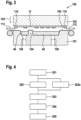
- Fig. 3 is a tool 100 for producing the module 10 not according to the invention according to Figure 1 or the module 10a according to the invention according to Figure 2
- the tool 100 comprises a lower tool part 101 and an upper tool part 102, which are arranged or designed to be movable relative to one another.
- the lower tool part 101 is arranged in a stationary manner
- the upper tool part 102 is adjustable in the direction of arrow 103 relative to the lower tool part 101.
- the carrier film 12 with its electrically conductive structures 18 is Top side 16 and bottom side 24 are attached to the upper tool part 102.
- a sealing web 104 can be seen, which is arranged in the area where no molding compound 46 is provided, ie in particular also in the detection area 32, 32a.
- the upper side of the lower tool part 101 is covered by a non-stick film 105.
- Molding compound 46 is already arranged in the area of two receiving spaces 106, 107 of the lower tool part 101, which are separated from each other by the sealing web 104.
- two compaction cylinders 108, 109 are provided at the base of the lower tool part 101, which are adjustable in the direction of the receptacles 106, 107 in order to enable compaction of the molding compound 46 in the receiving spaces 106, 107 when the tool 100 is closed.
- the interior of the tool 100 is also sealed from the external environment by means of seals 110 and can be evacuated by a vacuum source (not shown), which is indicated by the arrows 112.
- the tool 100 is removed from the Fig. 3 shown position into a position in which it is closed.
- the upper tool part 102 is moved in the direction of the lower tool part 101.
- the areas of the carrier film 12 on the underside 24 in which the molding compound 46 is to be arranged come into contact with the molding compound 46, at the latest when the compaction cylinders 108, 109 are moved in the direction of the receptacles 106, 107, whereby additional compaction of the molding compound 46 can then take place.
- the upper mold part 102 is moved back into a raised position to allow the module 10, 10a to be removed from the mold 100. Subsequently, further assembly of electronic components takes place on the module 10, 10a, for example, the connector 28 or at the locations where no molding compound 46 is provided.
- a first step 201 the carrier film 12 is provided, wherein the carrier film 12 has the electrically conductive structures 18. If necessary, electronic components of the electronic circuit 14 can also be mounted (in particular on the side of the carrier film 12 on which no molding compound 46 is provided).
- a second step 202 not according to the invention, the structure 34 is formed in the detection area 32 in the event that the structure 34 is formed directly on the carrier film 12.
- a second step 202a instead of the second step 202, a second step 202a according to the invention can be provided, in which the detection film 54 is connected to the carrier film 12 in the detection area 32a using suitable techniques.
- a third step 203 further assembly of the module 10, 10a with electronic components can take place, if necessary.
- This assembly also includes, in particular, contacting the structure 34 or the detection film 54 with the evaluation ICs 36, 38, if this has not already taken place.
- the carrier film 12 is partially remolded with the molding compound 46, as already explained above in connection with the tool 100. It is essential that the detection area 32, 32a is free of molding compound 46.
- a fifth step 205 further assembly of components on the module 10, 10a can take place.
- the module 10a described so far can be modified in a variety of ways without deviating from the idea of the invention defined in the claims.
- the present invention has been explained using a pressure sensor 30a.
- the invention is also intended to be applied to other sensors in which it is necessary to detect a deformation of an (elastic) membrane or an elastically deformable detection area 32, 32a.
- a flow sensor is mentioned as an example.
Landscapes
- Chemical & Material Sciences (AREA)
- Analytical Chemistry (AREA)
- Physics & Mathematics (AREA)
- General Physics & Mathematics (AREA)
- Measuring Fluid Pressure (AREA)
Claims (9)
- Module électronique (10 ; 10a), comprenant un film porteur (12), dans lequel au moins une structure électriquement conductrice (18) et des composants électroniques (26, 28) reliés à la structure électriquement conductrice (18) sont disposés sur le film porteur (12) en faisant partie d'un circuit électronique (14), dans lequel le circuit électronique (14) est relié à un capteur, en particulier à un capteur de pression (30 ; 30a), et dans lequel le film porteur (12) est recouvert au moins par endroits d'une masse de protection (45) sur une face supérieure (16) ou une face inférieure (24),dans lequel le capteur, en particulier le capteur de pression (30 ; 30a) présente une zone de détection (32 ; 32a) déformable élastiquement, caractérisé en ce que la zone de détection (32, 32a) est formée par une zone partielle du film porteur (12) et de plus par un film de détection (54), relié au film porteur (12), avec une microstructuration, dans lequel le film de détection (54) estcomposé de silicium pour obtenir une mise en contact du film de détection (54), protégée contre des contraintes mécaniques et des milieux, en ce que des moyens pour détecter la déformation de la zone de détection (32 ; 32a) sont prévus, et en ce que la masse de protection (45) ou un corps de fixation présente un évidement (48) à l'intérieur duquel le film porteur (12) et le film de détection (54) sont exposés, dans lequel l'évidement (48) délimite sur le bord la zone de détection (32 ; 32a) de sorte que la masse de protection (45) ou le corps de fixation fixe la zone de détection (32 ; 32a) par rapport au film porteur (12), dans lequel la paroi de l'évidement (48) s'étend légèrement en biais de sorte que le diamètre de l'évidement (48) augmente avec une distance croissante du film porteur.
- Module électronique selon la revendication 1,
caractérisé
en ce que les moyens de détection de la déformation de la zone de détection (32 ; 32a) sont formés par le film de détection (54), en particulier de telle sorte qu'une résistance électrique du film de détection (54) change en fonction de la déformation de la zone de détection (32 ; 32a). - Module électronique selon l'une quelconque des revendications 1 ou 2,
caractérisé
en ce que le film porteur (12) présente sur la face opposée à la zone de détection (32) une zone de détection supplémentaire (42) alignée sur la zone de détection (32), dans lequel la taille de la zone de détection supplémentaire (42) correspond au maximum à la taille de la zone de détection (32). - Module électronique selon la revendication 3,
caractérisé
en ce que la face du film porteur (12) sur laquelle se trouve la zone de détection supplémentaire (42) est exempte de la masse de protection (45). - Module électronique selon l'une quelconque des revendications 1 à 4,
caractérisé
en ce que le film de détection (54) est relié électriquement au moyen de liaisons filaires soudées (56, 58) à la structure électriquement conductrice (18) du film porteur (12) et la zone des liaisons filaires soudées (56, 58) est recouverte de la masse de protection (45). - Module électronique selon l'une quelconque des revendications 1 à 5,
caractérisé
en ce que les moyens de détection de la déformation de la zone de détection (32 ; 32a) comprennent une électronique d'évaluation (36, 38) qui est recouverte de la masse de protection (45). - Module électronique selon l'une quelconque des revendications 1 à 6,
caractérisé
en ce que la masse de protection (45) est formée par une masse moulée (46). - Procédé permettant de fabriquer un module électronique (10 ; 10a) qui est réalisé selon l'une quelconque des revendications 1 à 7, comprenant au moins les étapes suivantes consistant à :- fournir un film porteur (12) présentant au moins une structure électriquement conductrice (18),- relier au film porteur (12) un film de détection (54) détectant une déformation d'une zone de détection (32a) du film porteur (12),- réaliser au moins partiellement un circuit électronique (14) en équipant la structure électriquement conductrice (18) de composants électroniques,- recouvrir partiellement le film porteur (12) d'une masse de protection (45) ou appliquer un corps de fixation au film porteur (12) en dégageant la zone de détection (32 ; 32a),- le cas échéant équiper le film porteur (12) dans des zones où aucune masse de protection (45) n'est disposée.
- Procédé selon la revendication 8,
caractérisé
en ce que le film de détection (54) est relié à la structure électriquement conductrice (18) au moyen de liaisons filaires soudées (56, 58) avant le recouvrement du film porteur (12) avec la masse de protection (45), et en ce que les liaisons filaires soudées (56, 68) sont recouvertes de la masse de protection (45).
Applications Claiming Priority (1)
| Application Number | Priority Date | Filing Date | Title |
|---|---|---|---|
| DE102019205149.9A DE102019205149A1 (de) | 2019-04-10 | 2019-04-10 | Elektronisches Modul und Verfahren zu dessen Herstellung |
Publications (2)
| Publication Number | Publication Date |
|---|---|
| EP3722769A1 EP3722769A1 (fr) | 2020-10-14 |
| EP3722769B1 true EP3722769B1 (fr) | 2025-05-14 |
Family
ID=70108107
Family Applications (1)
| Application Number | Title | Priority Date | Filing Date |
|---|---|---|---|
| EP20166929.8A Active EP3722769B1 (fr) | 2019-04-10 | 2020-03-31 | Module électronique et son procédé de fabrication |
Country Status (2)
| Country | Link |
|---|---|
| EP (1) | EP3722769B1 (fr) |
| DE (1) | DE102019205149A1 (fr) |
Families Citing this family (1)
| Publication number | Priority date | Publication date | Assignee | Title |
|---|---|---|---|---|
| EP4014841A1 (fr) * | 2020-12-18 | 2022-06-22 | InnoME GmbH | Composant composite doté d'un élément de matière en mousse ou en élastomère |
Citations (3)
| Publication number | Priority date | Publication date | Assignee | Title |
|---|---|---|---|---|
| WO2005058133A2 (fr) * | 2003-12-11 | 2005-06-30 | Proteus Biomedical, Inc. | Capteurs de pression implantables |
| DE102007011472A1 (de) * | 2007-03-07 | 2008-09-11 | Metallux Ag | Drucksensitive Membran für einen elektronischen Sensor |
| WO2018235087A1 (fr) * | 2017-06-22 | 2018-12-27 | Ezmems Ltd. | Éléments capteurs sur feuilles/films minces |
Family Cites Families (7)
| Publication number | Priority date | Publication date | Assignee | Title |
|---|---|---|---|---|
| US7426873B1 (en) * | 2006-05-04 | 2008-09-23 | Sandia Corporation | Micro electro-mechanical system (MEMS) pressure sensor for footwear |
| DE102009001932A1 (de) | 2009-03-27 | 2010-09-30 | Robert Bosch Gmbh | Chipmodul und Verfahren zur Herstellung eines Chipmoduls |
| DE102010064120B4 (de) * | 2010-12-23 | 2023-05-25 | Robert Bosch Gmbh | Bauteil und Verfahren zu dessen Herstellung |
| DE102011004381A1 (de) * | 2011-02-18 | 2012-08-23 | Robert Bosch Gmbh | Moldmodul mit Sensorelement |
| AU2015253309B2 (en) * | 2014-04-28 | 2021-02-25 | The Regents Of The University Of California | Unobtrusive wireless electronic systems for monitoring and facilitating patient compliance |
| CN105404881A (zh) * | 2015-12-25 | 2016-03-16 | 成都费恩格尔微电子技术有限公司 | 一种指纹传感器组件及其制备方法 |
| CN106370325A (zh) * | 2016-11-07 | 2017-02-01 | 东北农业大学 | 工作座椅体压分布测试传感器 |
-
2019
- 2019-04-10 DE DE102019205149.9A patent/DE102019205149A1/de active Pending
-
2020
- 2020-03-31 EP EP20166929.8A patent/EP3722769B1/fr active Active
Patent Citations (3)
| Publication number | Priority date | Publication date | Assignee | Title |
|---|---|---|---|---|
| WO2005058133A2 (fr) * | 2003-12-11 | 2005-06-30 | Proteus Biomedical, Inc. | Capteurs de pression implantables |
| DE102007011472A1 (de) * | 2007-03-07 | 2008-09-11 | Metallux Ag | Drucksensitive Membran für einen elektronischen Sensor |
| WO2018235087A1 (fr) * | 2017-06-22 | 2018-12-27 | Ezmems Ltd. | Éléments capteurs sur feuilles/films minces |
Also Published As
| Publication number | Publication date |
|---|---|
| DE102019205149A1 (de) | 2020-10-15 |
| EP3722769A1 (fr) | 2020-10-14 |
Similar Documents
| Publication | Publication Date | Title |
|---|---|---|
| EP2167930B1 (fr) | Unité de raccordement pour une cellule de mesure de pression | |
| DE102010064120B4 (de) | Bauteil und Verfahren zu dessen Herstellung | |
| DE102011084582B3 (de) | Mikromechanische Sensorvorrichtung mit Moldverpackung und entsprechendes Herstellungsverfahren | |
| EP3304021B1 (fr) | Dispositif servant à détecter une pression d'un milieu fluide et procédé servant à fabriquer le dispositif | |
| DE102004011702B4 (de) | Verfahren zur Herstellung eines Kartenkörpers für eine kontaktlose Chipkarte | |
| EP2235492A1 (fr) | Module de mesure de pression | |
| DE102014112495B4 (de) | Sensoranordnung und Verfahren zu dessen Herstellung | |
| EP2526545B1 (fr) | Capteur a attenuation | |
| DE102013214915A1 (de) | Verdrahtungseinrichtung zum Verdrahten einer elektronischen Vorrichtung | |
| WO2010028884A2 (fr) | Encapsulage, système micro-électromécanique et procédé d'encapsulage | |
| EP2379998A1 (fr) | Dispositif et procédé de fabrication du dispositif | |
| WO2012100861A1 (fr) | Élément et procédé de fabrication correspondant | |
| DE102010042987A1 (de) | Verfahren zum Herstellen einer elektrischen Schaltung und elektrische Schaltung | |
| WO2014095500A1 (fr) | Procédé de fabrication d'un ensemble électronique | |
| EP3722769B1 (fr) | Module électronique et son procédé de fabrication | |
| EP2700248B1 (fr) | Dispositif micro-électromécanique de détection acoustique et son procédé de fabrication | |
| DE102006031047A1 (de) | Halbleitersensor und Herstellungsverfahren dafür | |
| DE102011085471B4 (de) | Anordnung zur Direktkontaktierung von Kontaktmitteln und zugehörige Anschlusseinheit für eine Druckmesszelle | |
| EP2340693B1 (fr) | Procédé de fabrication d'un circuit électrique | |
| EP3289840A1 (fr) | Module électronique pour appareil de commande de transmission | |
| WO2015078959A1 (fr) | Procédé permettant de produire un module électronique | |
| DE102012222491B4 (de) | Elektronisches Bauteil mit einem gespritzten Bauteilgehäuse | |
| EP3256820B1 (fr) | Module de commande de transmission | |
| DE102021204645A1 (de) | Verfahren zur Herstellung eines mikroelektromechanischen Sensors aus einem MEMS-Element und einem ASIC-Element und mikroelektromechanischer Sensor | |
| WO2018068921A1 (fr) | Dispositif de détection pour véhicule, véhicule automobile |
Legal Events
| Date | Code | Title | Description |
|---|---|---|---|
| PUAI | Public reference made under article 153(3) epc to a published international application that has entered the european phase |
Free format text: ORIGINAL CODE: 0009012 |
|
| STAA | Information on the status of an ep patent application or granted ep patent |
Free format text: STATUS: THE APPLICATION HAS BEEN PUBLISHED |
|
| AK | Designated contracting states |
Kind code of ref document: A1 Designated state(s): AL AT BE BG CH CY CZ DE DK EE ES FI FR GB GR HR HU IE IS IT LI LT LU LV MC MK MT NL NO PL PT RO RS SE SI SK SM TR |
|
| AX | Request for extension of the european patent |
Extension state: BA ME |
|
| STAA | Information on the status of an ep patent application or granted ep patent |
Free format text: STATUS: REQUEST FOR EXAMINATION WAS MADE |
|
| 17P | Request for examination filed |
Effective date: 20210414 |
|
| RBV | Designated contracting states (corrected) |
Designated state(s): AL AT BE BG CH CY CZ DE DK EE ES FI FR GB GR HR HU IE IS IT LI LT LU LV MC MK MT NL NO PL PT RO RS SE SI SK SM TR |
|
| STAA | Information on the status of an ep patent application or granted ep patent |
Free format text: STATUS: EXAMINATION IS IN PROGRESS |
|
| 17Q | First examination report despatched |
Effective date: 20220511 |
|
| GRAP | Despatch of communication of intention to grant a patent |
Free format text: ORIGINAL CODE: EPIDOSNIGR1 |
|
| STAA | Information on the status of an ep patent application or granted ep patent |
Free format text: STATUS: GRANT OF PATENT IS INTENDED |
|
| GRAJ | Information related to disapproval of communication of intention to grant by the applicant or resumption of examination proceedings by the epo deleted |
Free format text: ORIGINAL CODE: EPIDOSDIGR1 |
|
| STAA | Information on the status of an ep patent application or granted ep patent |
Free format text: STATUS: EXAMINATION IS IN PROGRESS |
|
| INTG | Intention to grant announced |
Effective date: 20241122 |
|
| GRAP | Despatch of communication of intention to grant a patent |
Free format text: ORIGINAL CODE: EPIDOSNIGR1 |
|
| STAA | Information on the status of an ep patent application or granted ep patent |
Free format text: STATUS: GRANT OF PATENT IS INTENDED |
|
| INTC | Intention to grant announced (deleted) | ||
| INTG | Intention to grant announced |
Effective date: 20250120 |
|
| GRAS | Grant fee paid |
Free format text: ORIGINAL CODE: EPIDOSNIGR3 |
|
| GRAA | (expected) grant |
Free format text: ORIGINAL CODE: 0009210 |
|
| STAA | Information on the status of an ep patent application or granted ep patent |
Free format text: STATUS: THE PATENT HAS BEEN GRANTED |
|
| AK | Designated contracting states |
Kind code of ref document: B1 Designated state(s): AL AT BE BG CH CY CZ DE DK EE ES FI FR GB GR HR HU IE IS IT LI LT LU LV MC MK MT NL NO PL PT RO RS SE SI SK SM TR |
|
| REG | Reference to a national code |
Ref country code: GB Ref legal event code: FG4D Free format text: NOT ENGLISH |
|
| REG | Reference to a national code |
Ref country code: CH Ref legal event code: EP |
|
| REG | Reference to a national code |
Ref country code: IE Ref legal event code: FG4D Free format text: LANGUAGE OF EP DOCUMENT: GERMAN |
|
| REG | Reference to a national code |
Ref country code: DE Ref legal event code: R096 Ref document number: 502020011043 Country of ref document: DE |
|
| REG | Reference to a national code |
Ref country code: NL Ref legal event code: MP Effective date: 20250514 |
|
| PG25 | Lapsed in a contracting state [announced via postgrant information from national office to epo] |
Ref country code: FI Free format text: LAPSE BECAUSE OF FAILURE TO SUBMIT A TRANSLATION OF THE DESCRIPTION OR TO PAY THE FEE WITHIN THE PRESCRIBED TIME-LIMIT Effective date: 20250514 Ref country code: PT Free format text: LAPSE BECAUSE OF FAILURE TO SUBMIT A TRANSLATION OF THE DESCRIPTION OR TO PAY THE FEE WITHIN THE PRESCRIBED TIME-LIMIT Effective date: 20250915 Ref country code: ES Free format text: LAPSE BECAUSE OF FAILURE TO SUBMIT A TRANSLATION OF THE DESCRIPTION OR TO PAY THE FEE WITHIN THE PRESCRIBED TIME-LIMIT Effective date: 20250514 |
|
| REG | Reference to a national code |
Ref country code: LT Ref legal event code: MG9D |
|
| PG25 | Lapsed in a contracting state [announced via postgrant information from national office to epo] |
Ref country code: NO Free format text: LAPSE BECAUSE OF FAILURE TO SUBMIT A TRANSLATION OF THE DESCRIPTION OR TO PAY THE FEE WITHIN THE PRESCRIBED TIME-LIMIT Effective date: 20250814 Ref country code: GR Free format text: LAPSE BECAUSE OF FAILURE TO SUBMIT A TRANSLATION OF THE DESCRIPTION OR TO PAY THE FEE WITHIN THE PRESCRIBED TIME-LIMIT Effective date: 20250815 |
|
| PG25 | Lapsed in a contracting state [announced via postgrant information from national office to epo] |
Ref country code: PL Free format text: LAPSE BECAUSE OF FAILURE TO SUBMIT A TRANSLATION OF THE DESCRIPTION OR TO PAY THE FEE WITHIN THE PRESCRIBED TIME-LIMIT Effective date: 20250514 Ref country code: NL Free format text: LAPSE BECAUSE OF FAILURE TO SUBMIT A TRANSLATION OF THE DESCRIPTION OR TO PAY THE FEE WITHIN THE PRESCRIBED TIME-LIMIT Effective date: 20250514 |
|
| PG25 | Lapsed in a contracting state [announced via postgrant information from national office to epo] |
Ref country code: BG Free format text: LAPSE BECAUSE OF FAILURE TO SUBMIT A TRANSLATION OF THE DESCRIPTION OR TO PAY THE FEE WITHIN THE PRESCRIBED TIME-LIMIT Effective date: 20250514 |
|
| PG25 | Lapsed in a contracting state [announced via postgrant information from national office to epo] |
Ref country code: HR Free format text: LAPSE BECAUSE OF FAILURE TO SUBMIT A TRANSLATION OF THE DESCRIPTION OR TO PAY THE FEE WITHIN THE PRESCRIBED TIME-LIMIT Effective date: 20250514 |
|
| PG25 | Lapsed in a contracting state [announced via postgrant information from national office to epo] |
Ref country code: RS Free format text: LAPSE BECAUSE OF FAILURE TO SUBMIT A TRANSLATION OF THE DESCRIPTION OR TO PAY THE FEE WITHIN THE PRESCRIBED TIME-LIMIT Effective date: 20250814 |
|
| PG25 | Lapsed in a contracting state [announced via postgrant information from national office to epo] |
Ref country code: IS Free format text: LAPSE BECAUSE OF FAILURE TO SUBMIT A TRANSLATION OF THE DESCRIPTION OR TO PAY THE FEE WITHIN THE PRESCRIBED TIME-LIMIT Effective date: 20250914 |
|
| PG25 | Lapsed in a contracting state [announced via postgrant information from national office to epo] |
Ref country code: LV Free format text: LAPSE BECAUSE OF FAILURE TO SUBMIT A TRANSLATION OF THE DESCRIPTION OR TO PAY THE FEE WITHIN THE PRESCRIBED TIME-LIMIT Effective date: 20250514 |
|
| PG25 | Lapsed in a contracting state [announced via postgrant information from national office to epo] |
Ref country code: DK Free format text: LAPSE BECAUSE OF FAILURE TO SUBMIT A TRANSLATION OF THE DESCRIPTION OR TO PAY THE FEE WITHIN THE PRESCRIBED TIME-LIMIT Effective date: 20250514 Ref country code: SM Free format text: LAPSE BECAUSE OF FAILURE TO SUBMIT A TRANSLATION OF THE DESCRIPTION OR TO PAY THE FEE WITHIN THE PRESCRIBED TIME-LIMIT Effective date: 20250514 |
|
| PG25 | Lapsed in a contracting state [announced via postgrant information from national office to epo] |
Ref country code: CZ Free format text: LAPSE BECAUSE OF FAILURE TO SUBMIT A TRANSLATION OF THE DESCRIPTION OR TO PAY THE FEE WITHIN THE PRESCRIBED TIME-LIMIT Effective date: 20250514 |
|
| PG25 | Lapsed in a contracting state [announced via postgrant information from national office to epo] |
Ref country code: EE Free format text: LAPSE BECAUSE OF FAILURE TO SUBMIT A TRANSLATION OF THE DESCRIPTION OR TO PAY THE FEE WITHIN THE PRESCRIBED TIME-LIMIT Effective date: 20250514 |
|
| PG25 | Lapsed in a contracting state [announced via postgrant information from national office to epo] |
Ref country code: SK Free format text: LAPSE BECAUSE OF FAILURE TO SUBMIT A TRANSLATION OF THE DESCRIPTION OR TO PAY THE FEE WITHIN THE PRESCRIBED TIME-LIMIT Effective date: 20250514 Ref country code: RO Free format text: LAPSE BECAUSE OF FAILURE TO SUBMIT A TRANSLATION OF THE DESCRIPTION OR TO PAY THE FEE WITHIN THE PRESCRIBED TIME-LIMIT Effective date: 20250514 |
|
| PG25 | Lapsed in a contracting state [announced via postgrant information from national office to epo] |
Ref country code: IT Free format text: LAPSE BECAUSE OF FAILURE TO SUBMIT A TRANSLATION OF THE DESCRIPTION OR TO PAY THE FEE WITHIN THE PRESCRIBED TIME-LIMIT Effective date: 20250514 |
|
| REG | Reference to a national code |
Ref country code: DE Ref legal event code: R097 Ref document number: 502020011043 Country of ref document: DE |
|
| PLBE | No opposition filed within time limit |
Free format text: ORIGINAL CODE: 0009261 |
|
| STAA | Information on the status of an ep patent application or granted ep patent |
Free format text: STATUS: NO OPPOSITION FILED WITHIN TIME LIMIT |
|
| REG | Reference to a national code |
Ref country code: CH Ref legal event code: L10 Free format text: ST27 STATUS EVENT CODE: U-0-0-L10-L00 (AS PROVIDED BY THE NATIONAL OFFICE) Effective date: 20260325 |
|
| PGFP | Annual fee paid to national office [announced via postgrant information from national office to epo] |
Ref country code: GB Payment date: 20260324 Year of fee payment: 7 |
|
| PGFP | Annual fee paid to national office [announced via postgrant information from national office to epo] |
Ref country code: FR Payment date: 20260325 Year of fee payment: 7 |
|
| 26N | No opposition filed |
Effective date: 20260217 |