EP3731422B1 - Puce de circuit intégré - Google Patents
Puce de circuit intégré Download PDFInfo
- Publication number
- EP3731422B1 EP3731422B1 EP18892943.4A EP18892943A EP3731422B1 EP 3731422 B1 EP3731422 B1 EP 3731422B1 EP 18892943 A EP18892943 A EP 18892943A EP 3731422 B1 EP3731422 B1 EP 3731422B1
- Authority
- EP
- European Patent Office
- Prior art keywords
- reception
- chip
- circuit
- input unit
- arrangement
- Prior art date
- Legal status (The legal status is an assumption and is not a legal conclusion. Google has not performed a legal analysis and makes no representation as to the accuracy of the status listed.)
- Active
Links
Images


Classifications
-
- H—ELECTRICITY
- H02—GENERATION; CONVERSION OR DISTRIBUTION OF ELECTRIC POWER
- H02H—EMERGENCY PROTECTIVE CIRCUIT ARRANGEMENTS
- H02H9/00—Emergency protective circuit arrangements for limiting excess current or voltage without disconnection
- H02H9/04—Emergency protective circuit arrangements for limiting excess current or voltage without disconnection responsive to excess voltage
- H02H9/045—Emergency protective circuit arrangements for limiting excess current or voltage without disconnection responsive to excess voltage adapted to a particular application and not provided for elsewhere
- H02H9/046—Emergency protective circuit arrangements for limiting excess current or voltage without disconnection responsive to excess voltage adapted to a particular application and not provided for elsewhere responsive to excess voltage appearing at terminals of integrated circuits
-
- H—ELECTRICITY
- H10—SEMICONDUCTOR DEVICES; ELECTRIC SOLID-STATE DEVICES NOT OTHERWISE PROVIDED FOR
- H10W—GENERIC PACKAGES, INTERCONNECTIONS, CONNECTORS OR OTHER CONSTRUCTIONAL DETAILS OF DEVICES COVERED BY CLASS H10
- H10W42/00—Arrangements for protection of devices
- H10W42/60—Arrangements for protection of devices protecting against electrostatic charges or discharges, e.g. Faraday shields
-
- H—ELECTRICITY
- H03—ELECTRONIC CIRCUITRY
- H03H—IMPEDANCE NETWORKS, e.g. RESONANT CIRCUITS; RESONATORS
- H03H7/00—Multiple-port networks comprising only passive electrical elements as network components
- H03H7/01—Frequency selective two-port networks
- H03H7/0138—Electrical filters or coupling circuits
-
- H—ELECTRICITY
- H04—ELECTRIC COMMUNICATION TECHNIQUE
- H04B—TRANSMISSION
- H04B3/00—Line transmission systems
- H04B3/02—Details
-
- H—ELECTRICITY
- H10—SEMICONDUCTOR DEVICES; ELECTRIC SOLID-STATE DEVICES NOT OTHERWISE PROVIDED FOR
- H10W—GENERIC PACKAGES, INTERCONNECTIONS, CONNECTORS OR OTHER CONSTRUCTIONAL DETAILS OF DEVICES COVERED BY CLASS H10
- H10W44/00—Electrical arrangements for controlling or matching impedance
Definitions
- the present invention relates to an IC chip which includes a compact wideband DC-blocking circuit.
- the ICs When high-speed electrical signal communication is performed between ICs (Integrated Circuits), the ICs are generally connected by a transmission line (transmission medium) in which a characteristic impedance Z0 is 50 ⁇ .
- a 50- ⁇ resistor for impedance matching is arranged on each of the transmission-end side and the reception-end side of the transmission line.
- a DC-blocking capacitor that cuts off the DC component of a signal is arranged between the ICs.
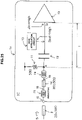
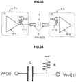
- Fig. 33 shows an example of a general signal transmission/reception arrangement which includes a DC-blocking capacitor.
- a transmission-side circuit 10-1 and a 50- ⁇ resistor 11-1 for impedance matching are arranged in a transmission-side IC 1-1
- a reception-side circuit 10-2 and a 50- ⁇ resistor 11-2 for impedance matching are arranged in a transmission-side IC 1-2.
- the IC 1-1 and the IC 1-2 are connected by a transmission line 101, and a DC-blocking capacitor 3 is arranged in the middle of the transmission line 101.
- the capacitor C needs to be set to about 5 nF or more (nF order) to implement a cutoff frequency of about 1 MHz. It is difficult, in terms of the dedicated area, to manufacture an nF-order capacitor on a chip by a general semiconductor process, and a DC-blocking capacitor needs to be mounted externally (off the chip) (see non-patent literature 1).
- US 2013/002347 A1 discloses an integrated circuit according to the preamble of claim 1.
- Non-Patent Literature 1 H. Wakita, et al., "36-GHz-Bandwidth Quad-channel Driver Module using Compact QFN Package for Optical Coherent Systems", Electrical Performance of Electronic Packaging and Systems (EPEPS), 2015
- the present invention has been made to solve the above-described problem and has as its object to implement a compact wideband DC-blocking circuit that can be mounted on an IC chip while ensuring impedance matching.
- the present application discloses a IC chip comprising: a pad (15) connected to a first transmission line (2) outside the chip; a signal line (16), one end of which is connected to the pad; a termination resistor (11) connected to the other end of the signal line and configured to terminate the first transmission line; a reception-side input unit circuit (10) configured to receive a signal transmitted from a transmission-side via the first transmission line; and a capacitor (12) inserted between a node (A) of the signal line and the termination resistor and an input terminal of the reception-side input unit circuit, characterized in that a length (L) from the node of the signal line and the termination resistor to the input terminal of the reception-side input unit circuit is shorter than a wavelength of a maximum frequency component of a signal handled by the reception-side input unit circuit.
- the present invention provides a compact wideband DC-blocking circuit that can be mounted on an IC chip while ensuring 50- ⁇ impedance matching.
- a blocking capacitor which is conventionally arranged on a transmission line between a transmission-side IC chip and a reception-side IC chip, is arranged on the reception-side IC chip.
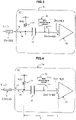
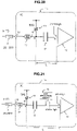
- FIG. 1 is a circuit diagram showing a reception-side IC chip according to the first embodiment of the present invention.
- a reception-side IC chip 1a at least includes a pad 15 connected to a transmission line 2 whose characteristic impedance Z0 from outside the chip is 50 ⁇ , a signal line 16, one end of which is connected to the pad 15, a reception-side input unit circuit 10 that receives a signal S transmitted from a transmission-side IC chip (not shown) via the transmission line 2, a 50- ⁇ termination resistor 11 for impedance matching that is connected between a predetermined voltage and the other end of the signal line 16 and terminates the transmission line 2, and a capacitor 12 inserted between a node A of the signal line 16 and the termination resistor 11 and an input terminal In of the reception-side input unit circuit 10.
- an on-chip DC-blocking circuit is formed by the capacitor 12.
- an input impedance Zin of the reception-side input unit circuit 10 needs to be increased to make the capacitor 12 be of a size that can be mounted on a chip.
- the degree to which the input impedance Zin is to be set will be described later.
- FIG. 2 is a circuit diagram showing the arrangement of a reception-side IC chip according to the second embodiment of the present invention.
- a reception-side IC chip 1b according to this embodiment has the same arrangement as the first embodiment, but is characterized in that a length L from a node A of a signal line 16 and a termination resistor 11 to an input terminal In of a reception-side input unit circuit 10 is sufficiently shorter than the wavelength of a maximum frequency component of a signal S handled by the reception-side IC chip 1b (reception-side input unit circuit 10).
- the length L can be set to be less than 1/20 of the wavelength of the maximum frequency component of the signal S handled by the reception-side IC chip 1b (reception-side input unit circuit 10).
- a circuit whose length L is of a size less than 1/20 of a signal wavelength can be handled as a lumped constant circuit. That is, as long as the size is less than 1/20 of the signal wavelength, the signal waveform will not be influenced even under a state in which a reflected wave or the like will occur.
- FIG. 3 is a circuit diagram showing the arrangement of a reception-side IC chip according to the third embodiment of the present invention.
- a reception-side IC chip 1c according to this embodiment is obtained by adding, to the arrangement of the first embodiment, a bias application circuit 13 that applies a DC bias voltage to an input terminal In of a reception-side input unit circuit 10.
- an input impedance Zin of the reception-side input unit circuit 10 and an output impedance Zout of the bias application circuit 13 need to be increased.
- the degrees to which the input impedance Zin and the output impedance Zout are to be set will be described later.
- FIG. 4 is a circuit diagram showing the arrangement of a reception-side IC chip according to the fourth embodiment of the present invention.
- a reception-side IC chip 1d according to this embodiment has the same arrangement as the third embodiment, but is characterized in that a length L from a node A of a signal line 16 and a termination resistor 11 to an input terminal In of a reception-side input unit circuit 10 is sufficiently shorter than the wavelength of a maximum frequency component of a signal S handled by the reception-side IC chip 1d (reception-side input unit circuit 10).
- the length L can be set to be less than 1/20 of the wavelength of the maximum frequency component of the signal S handled by the reception-side IC chip 1d (reception-side input unit circuit 10).
- a DC-blocking circuit arrangement that has the characteristics described in the first to fourth embodiments, impedance matching by the 50- ⁇ termination resistor 11 arranged before a capacitor 12 can be ensured and a resistance value R, as indicated in the circuit shown in Fig. 34 , can be designed to be sufficiently large when the reception-side input unit circuit 10 is viewed from the node A of the signal line 16 and the termination resistor 11. As a result, the cutoff frequency of a high-pass filter can be extended to a low frequency range even if the value of the capacitor 12 is reduced.
- a high-pass filter is formed by the capacitor 12 and an input impedance Zin of the reception-side input unit circuit 10.
- the input impedance Zin (the value of the resistor R) can be set based on equation (1) so that the cutoff frequency of the high-pass filter and the capacitance of the capacitor 12 become desired values, respectively.
- a high-pass filter is formed by the capacitor 12 and a combined resistance of the input impedance Zin of the reception-side input unit circuit 10 and an output impedance Zout of a bias application circuit 13.
- the input impedance Zin and the output impedance Zout can be set so that the cutoff frequency of the high-pass filter and the capacitance of the capacitor 12 become desired values, respectively.
- the capacitance value of the capacitor 12 necessary to implement a cutoff frequency of 1 MHz can be 1 pF or less. That is, the capacitor 12 will be of a size that can be mounted on a chip.
- the length L from the node A of the signal line 16 and the termination resistor 11 to the input terminal In of the reception-side input unit circuit 10 to be sufficiently shorter than the wavelength of the maximum frequency component of the signal S to be handled, characteristic degradation (the influence from the reflection due to impedance mismatch between the node A and the reception-side input unit circuit 10) at the high-frequency range can be suppressed.
- a compact wideband DC-blocking circuit which is mountable on an IC chip can be implemented while ensuring 50- ⁇ impedance matching.
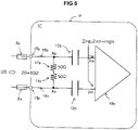
- FIG. 5 is a circuit diagram showing the arrangement of a reception-side IC chip according to the fifth embodiment of the present invention.
- a reception-side IC chip 1e at least includes a pad 15p connected to a non-inverting-side transmission line 2p whose characteristic impedance Z0 is 50 ⁇ , a pad 15n connected to an inverting-side transmission line 2n whose characteristic impedance z0 is 50 ⁇ , a signal line 16p, one end of which is connected to the pad 15p, a signal line 16n, one end of which is connected to the pad 15n, a reception-side input unit circuit 10e which receives a differential signal DS from a transmission-side IC chip (not shown) via the transmission lines 2p and 2n having a differential arrangement, a 50- ⁇ termination resistor 11p for impedance matching which is connected between a predetermined voltage and the other end of the signal line 16p and terminates the transmission line 2p, a 50- ⁇ termination resistor 11n for impedance matching which is connected between a predetermined voltage and the other end of the signal line 16n and terminates the transmission line 2n, a capacitor 12p inserted
- an on-chip DC-blocking circuit is formed by the capacitors 12p and 12n.
- each of the capacitors 12p and 12n be of a size that can be mounted on a chip
- the non-inverting-side input impedance Zinp and the inverting-side input impedance Zinn of the reception-side input unit circuit 10e need to be increased.
- the degrees to which the input impedances Zinp and Zinn are to be set will be described later.
- the termination resistors 11p and 11n for impedance matching in the differential circuit can be arranged in several kinds of ways, and may be arranged as a T-shaped termination, as shown in Fig. 5 , as a measure against common mode noise or may be arranged as a ⁇ -shaped termination as a reception-side IC chip 1f as shown in Fig.6 .
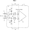
- FIG. 7 is a circuit diagram showing the arrangement of a reception-side IC chip according to the sixth embodiment of the present invention.
- a reception-side IC chip 1g according to this embodiment has the same arrangement as the fifth embodiment, but is characterized in that a length Lp, from a node Ap of a non-inverting-side signal line 16p and a termination resistor 11p to a non-inverting input terminal Inp of a reception-side input unit circuit 10e, and a length Ln, from a node An of an inverting-side signal line 16n and a termination resistor 11n to an inverting input terminal Inn of the reception-side input unit circuit 10e will be sufficiently shorter than the wavelength of the maximum frequency component of a signal DS handled by the reception-side IC chip 1g (reception-side input unit circuit 10e).
- the lengths Lp and Ln can be set to be less than 1/20 of the wavelength of the maximum frequency component of the signal DS handled by the reception-side IC chip 1g (reception-side input unit circuit 10e).
- a T-shaped termination as shown in Fig. 7 , may be arranged as a measure against common mode noise or a ⁇ -shaped termination as that of a reception-side IC chip 1h shown in Fig. 8 may be arranged.
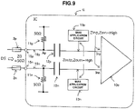
- FIG. 9 is a circuit diagram showing the arrangement of a reception-side IC chip according to the seventh embodiment of the present invention.
- a reception-side IC chip 1i according to the embodiment is obtained by adding, to the arrangement of the fifth embodiment, a bias application circuit 13p, which applies a DC bias voltage to a non-inverting input terminal Inp of the reception-side input unit circuit 10e, and a bias application circuit 13n, which applies a DC bias voltage to a inverting input terminal Inn of the reception-side input unit circuit 10e.
- capacitors 12p and 12n be of a size that can be mounted on a chip
- input impedances Zinp and Zinn of the reception-side input unit circuit 10e and output impedances Zoutp and Zoutn of the bias application circuits 13p and 13n need to be increased.
- the degrees to which the input impedances Zinp and Zinn and the output impedances Zoutp and Zoutn are to be set will be described later.
- a T-shaped terminal arrangement as shown in Fig. 9 , may be used as a measure against common mode noise or a ⁇ -shaped terminal arrangement as that of a reception-side IC chip 1j shown in Fig. 10 may be used.
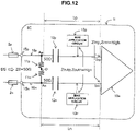
- FIG. 11 is a circuit diagram showing the arrangement of a reception-side IC chip according to the eighth embodiment of the present invention.
- a reception-side IC chip 1k according to the embodiment has the same arrangement as the seventh embodiment, but is characterized in that a length Lp, from a node Ap of a non-inverting-side signal line 16p and a termination resistor 11p to a non-inverting input terminal Inp of a reception-side input unit circuit 10e, and a length Ln, from a node An of an inverting-side signal line 16n and a termination resistor 11n to an inverting input terminal Inn of the reception-side input unit circuit 10e will be sufficiently shorter than the wavelength of the maximum frequency component of a differential signal DS handled by the reception-side IC chip 1k (reception-side input unit circuit 10e).
- the lengths Lp and Ln can be set to be less than 1/20 of the wavelength of the maximum frequency component
- a T-shaped termination as shown in Fig. 11 , may be arranged as a measure against common mode noise or a ⁇ -shaped termination as that of a reception-side IC chip 11 shown in Fig. 12 may be arranged.
- a high-pass filter is formed by a capacitor 12p and a non-inverting-side input impedance Zinp of the reception-side input unit circuit 10e.
- the input impedance Zinp (the value of a resistor R) can be set based on equation (1) so that the cutoff frequency of the high-pass filter and the capacitance of the capacitor 12p become desired values, respectively.
- the input impedance Zinn (the value of the resistor R) can be set so that the cutoff frequency of the high-pass filter and the capacitance of the capacitor 12n become desired values, respectively.
- a high-pass filter is formed by the capacitor 12p and a combined resistance of the non-inverting-side input impedance Zinp of the reception-side input unit circuit 10e and an output impedance Zoutp of a bias application circuit 13p.
- the input impedance Zinp and the output impedance Zoutp can be set so that the cutoff frequency of the high-pass filter and the capacitance of the capacitor 12p become desired values, respectively.
- the input impedance Zinn and the output impedance Zoutn can be set so that the cutoff frequency of the high-pass filter and the capacitance of the capacitor 12n become desired values, respectively.
- reception-side input unit circuit 10 that has a high input impedance needs to be arranged to implement the IC chip according to each of the first to fourth embodiments.
- a circuit which uses the base as an input is suitable in a case in which a bipolar transistor is to be used, and a circuit which uses the gate as an input is suitable in a case in which an FET (field effect transistor) is to be used.
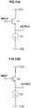
- a bipolar transistor it is preferable to use an emitter follower formed by a bipolar transistor Q1 and a current source IS1, as shown in Fig. 13A , as the arrangement of an input stage of the reception-side input unit circuit 10.
- a source follower formed by an FET Q2 and a current source IS2 as shown in Fig. 13B , as the arrangement of the input stage of the reception-side input unit circuit 10.
- reception-side input unit circuit 10e An example of the arrangement of a reception-side input unit circuit 10e according to each of the fifth to eighth embodiments will be described next.
- the reception-side input unit circuit 10e that has a high input impedance needs to be arranged to implement the IC chip according to each of the fifth to eighth embodiments.
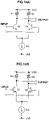
- a bipolar transistor it is preferable to use, as the arrangement of an input stage of the reception-side input unit circuit 10e, a differential circuit formed by bipolar transistors Q3 and Q4, resistors R1 and R2, and a current source IS3 as shown in Fig. 14A .
- a differential circuit formed by bipolar transistors Q3 and Q4, resistors R1 and R2, and a current source IS3 as shown in Fig. 14A .
- FET it is preferable to use, as the arrangement of the input stage of the reception-side input unit circuit 10e, a differential circuit formed by FETs Q5 and Q6, resistors R3 and R4, and a current source IS4 as shown in Fig. 14B .
- bias application circuit 13 can be implemented by a voltage divider circuit that is formed, for example, as shown in Fig.
- a resistor R5 in which one terminal is connected to a positive power supply voltage VCC (VDD in a case in which a reception-side input unit circuit 10 is formed by an FET) and the other terminal is connected to an output terminal of the bias application circuit 13, and a resistor R6 in which one terminal is connected to the output terminal of the bias application circuit 13 and the other terminal is connected to a negative power supply voltage VEE (VSS in the case in which the reception-side input unit circuit 10 is formed by an FET).
- VCC positive power supply voltage
- VEE negative power supply voltage
- bias application circuits 13p and 13n according to the seventh and eighth embodiments can also be implemented in the same manner by a voltage divider circuit.
- the resistance values of the resistors R5 and R6 need to be increased to increase output impedances Zout, Zoutp, and Zoutn of the bias application circuits 13, 13p, and 13n, respectively. More specifically, the values of the resistors R5 and R6 can be set in accordance with the respective bias voltages output from the bias application circuit 13, 13p, and 13n and the respective required output impedances Zout, Zoutp, and Zoutn.
- FIG. 16 is a circuit diagram showing the arrangement of a reception-side IC chip according to the 12th embodiment of the present invention.
- a reception-side IC chip 1m according to this embodiment is characterized in that a transmission line 14 having a characteristic impedance z0 of 50 ⁇ or more has been inserted in series to a signal line 16 of the arrangement according to the first embodiment or the second embodiment.
- the insertion of the transmission line 14 can suppress, in an input unit of the reception-side IC chip 1m, the influence of a parasitic capacitance from an input port (a signal input pad connected to a transmission line 2 or the like) to a termination resistor 11.
- the transmission line 14 can be applied to any of the first to eighth embodiments. If it is to be applied to the fifth to eighth embodiments, transmission lines 14p and 14n each having the characteristic impedance Z0 of 50 ⁇ or more can be inserted to signal lines 16p and 16n, respectively, as shown in Fig. 17 . Although the arrangement of Fig. 17 shows a case in which the transmission lines 14p and 14n are applied to Fig. 5 , they can also be applied to each of Figs. 6 to 12 in the same manner.
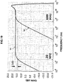
- the conventional arrangement uses an arrangement in which a capacitor 120 of 2.5 pF is inserted between the terminal of the transmission line 2 and a node of the termination resistor 11 and an input terminal of a reception-side input unit circuit 10.
- the arrangement of the present invention uses an arrangement in which the capacitance of a capacitor 12 in a reception-side IC chip 1d according to the fourth embodiment shown in Fig. 4 is 2.5 pF.
- Fig. 19 is a graph showing a frequency characteristic simulation results of the conventional reception-side IC chip and the reception-side IC chip of the present invention.
- reference numeral 180 indicates the frequency characteristic of the conventional reception-side IC chip
- reference numeral 181 indicates the frequency characteristic of the reception-side IC chip of the present invention.
- Fig. 19 it can be seen in Fig. 19 that using the arrangement of the present invention allows the cutoff frequency of a low frequency range to be extended from 600 MHz to 20 kHz without degrading high frequency characteristics.
- the present invention can be used to implement a compact wideband DC-blocking circuit that can be mounted on an IC chip.
- FIG. 20 is a circuit diagram showing the arrangement of a reception-side IC chip according to the 13th embodiment of the present invention.
- a reception-side IC chip 1n according to this embodiment is characterized in that an inductor 17 is inserted in series to a signal line 16 in the arrangement of the first embodiment or the second embodiment.
- the inductor 17 can be inserted as shown in Fig. 20 to suppress the degradation of the reflection characteristic.
- the inductor 17 since the inductor 17 has an inductance value of a small pH order, it can be regarded to be short-circuited in the low frequency range. Hence, the inductor 17 will not greatly influence the cutoff frequency of the low frequency range that needs to be ensured in the present invention.
- Fig. 21 shows the arrangement of a reception-side IC chip 1o obtained in a case in which the inductor 17 is applied to Fig. 3 according to the third embodiment or Fig. 4 according to the fourth embodiment.
- Fig. 22 shows the arrangement of a reception-side IC chip 1p obtained in a case in which inductors 17p and 17n are inserted in series to signal lines 16p and 16n, respectively, shown in Fig. 5 according to the fifth embodiment.
- the arrangement of Fig. 22 shows a case in which the inductors 17p and 17n are applied to Fig. 5
- the arrangement can be applied in the same manner to each of Figs. 6 to 8 .
- Fig. 23 shows the arrangement of a reception-side IC chip 1q obtained in a case in which the inductors 17p and 17n are inserted in series to the signal lines 16p and 16n, respectively, shown in Fig. 9 according to the seventh embodiment.
- the arrangement of Fig. 23 shows a case in which the inductors 17p and 17n are applied to Fig. 9
- the arrangement can be applied in the same manner to each of Figs. 10 to 12 .
- FIG. 24 is a circuit diagram showing the arrangement of a reception-side IC chip according to the 14th embodiment of the present invention.
- a reception-side IC chip 1r according to this embodiment is characterized in that an inductor 18 is inserted in series to a signal line 16 between a pad 15 and a transmission line 14 and an inductor 19 is inserted in series to the signal line 16 between the transmission line 14 and a node A of the signal line 16 and a termination resistor 11 in the arrangement according to the 12th embodiment.
- Fig. 25 shows the arrangement of a reception-side IC chip 1s obtained in a case in which the inductors 18 and 19 are applied to Fig. 3 according to the third embodiment or Fig. 4 according to the fourth embodiment.
- Fig. 26 shows the arrangement of a reception-side IC chip 1t obtained in a case in which inductors 18p and 19p and inductors 18n and 19n are inserted in series to signal lines 16p and 16n, respectively, shown in Fig. 17 according to the 12th embodiment.
- the arrangement of Fig. 26 shows a case in which the inductors 18p, 19p, 18n, and 19n are applied to Fig. 17
- the arrangement can be applied in the same manner to an arrangement obtained by serially inserting transmission lines 14p and 14n to the signal lines 16p and 16n, respectively, of each of Figs. 6 to 8 .
- Fig. 27 shows the arrangement of a reception-side IC chip 1u obtained in a case in which the transmission lines 14p and 14n are inserted in series to the signal lines 16p and 16n, respectively, and the inductors 18p and 19p and inductors 18n and 19n are inserted in series to the signal lines 16p and 16n, respectively, shown in Fig. 9 according to the seventh embodiment.
- the arrangement of Fig. 27 shows a case in which the inductors 18p, 19p, 18n, and 19n are applied to Fig. 9
- the arrangement can be applied in the same manner to an arrangement obtained by serially inserting the transmission lines 14p and 14n to the signal lines 16p and 16n, respectively, of each of Figs. 10 to 12 .
- Fig. 28 is a circuit diagram showing the arrangement of a reception-side IC chip according to the 15th embodiment of the present invention.
- a reception-side IC chip 1v according to this embodiment is characterized in that a transmission line 14 is formed by two transmission lines 14-1 and 14-2, which are connected in series, and an ESD (ElectroStatic Discharge) protection circuit 20, which is connected to a signal line 16 between the two transmission lines 14-1 and 14-2, are included in the arrangement according to the 14th embodiment shown in Fig. 24 .
- ESD ElectroStatic Discharge
- the ESD protection circuit 20 is arranged in the IC chip to improve ESD resistance.
- the two transmission lines 14-1 and 14-2 having a characteristic impedance Z0 of 50 ⁇ or more are arranged, and the ESD protection circuit 20 is arranged at the node of these two transmission lines 14-1 and 14-2.
- Fig. 29 shows the arrangement of the ESD protection circuit 20.
- the ESD protection circuit 20 is formed by N diodes D1, which are connected to set a reverse bias state between a positive power supply voltage VCC (VDD in a case in which a reception-side input unit circuit 10 is formed by an FET) and the signal line 16, and M diodes D2, which are connected to set a reverse bias state between a negative power supply voltage VEE (VSS in a case in which the reception-side input unit circuit 10 is formed by an FET) and the signal line 16.
- VCC positive power supply voltage
- VEE negative power supply voltage
- the stage counts N and M of the diodes D1 and D2, respectively, are parameters that are set arbitrarily to fall within a range in which the diodes D1 and D2 will not break down in accordance with the voltage (a DC operating point in an operation state) of the signal line 16. That is, N ⁇ 0 and M ⁇ 0.
- this embodiment can implement a compact and wideband DC-blocking circuit with high ESD resistance that can be mounted on an IC chip.
- Fig. 30 shows the arrangement of a reception-side IC chip 1w obtained in a case in which the transmission line 14 is formed by the two transmission lines 14-1 and 14-2 which are connected in series and an ESD (Electrostatic Discharge) protection circuit 20 is connected to the signal line 16 between the two transmission lines 14-1 and 14-2 in the arrangement shown in Fig. 25 according to the 14th embodiment.
- ESD Electrostatic Discharge
- Fig. 31 shows the arrangement of a reception-side IC chip 1x obtained in a case in which a transmission line 14p is formed by two transmission lines 14p-1 and 14p-2 having the characteristic impedance Z0 of 50 ⁇ or more, a transmission line 14n is formed by two transmission lines 14n-1 and 14n-2 having the characteristic impedance Z0 of 50 ⁇ or more, an ESD protection circuit 20p is connected to a signal line 16p between the two transmission lines 14p-1 and 14p-2 which are connected in series, and an ESD protection circuit 20n is connected to a signal line 16n between the two transmission lines 14n-1 and 14n-2 which are connected in series in the arrangement shown in Fig. 26 according to the 14th embodiment.
- each of the ESD protection circuits 20p and 20n is the same as the ESD protection circuit 20.
- the arrangement of Fig. 31 shows a case in which the ESD protection circuits 20p and 20n are applied to Fig. 26
- the arrangement can be applied in the same manner to an arrangement obtained by serially inserting the transmission lines 14p-1 and 14p-2 and inductors 18p and 19p to the signal line 16p and serially inserting the transmission lines 14n-1 and 14n-2 and inductors 18n and 19n to the signal line 16n in each of Figs. 6 to 8 .
- Fig. 32 shows the arrangement of a reception-side IC chip 1y obtained in a case in which the transmission line 14p is formed by the two transmission lines 14p-1 and 14p-2 having the characteristic impedance Z0 of 50 ⁇ or more, the transmission line 14n is formed by two transmission lines 14n-1 and 14n-2 having the characteristic impedance Z0 of 50 ⁇ or more, the ESD protection circuit 20p is connected to the signal line 16p between the two transmission lines 14p-1 and 14p-2 which are connected in series, and the ESD protection circuit 20n is connected to the signal line 16n between the two transmission lines 14n-1 and 14n-2 which are connected in series in the arrangement shown in Fig. 27 according to the 14th embodiment.
- the arrangement can be applied in the same manner to an arrangement obtained by serially inserting the transmission lines 14p-1 and 14p-2 and the inductors 18p and 19p to the signal line 16p and serially inserting the transmission lines 14n-1 and 14n-2 and the inductors 18n and 19n to the signal line 16n in each of Figs. 10 to 12 .
- the present invention can be applied to an IC chip that performs high-speed electrical signal communication.
- 1a-1y...reception-side IC chip 2, 2p, 2n, 14, 14-1, 14-2, 14p, 14p-1, 14p-2, 14n, 14n-1, 14n-2...transmission line, 10, 10e...reception-side input unit circuit, 11, 11p, 11n...termination resistor, 12, 12p, 12n...capacitor, 13, 13p, 13n...bias application circuit, 15, 15p, 15n...pad, 16, 16p, 16n...signal line, 17, 17p, 17n, 18, 18p, 18n, 19, 19p, 19n...inductor, 20, 20p, 20n...ESD protection circuit, Q1, Q3, Q4...bipolar transistor, Q2, Q5, Q6...FET, IS1 - IS4...current source, R1 - R6...resistor, D1, D2...diode.
Landscapes
- Engineering & Computer Science (AREA)
- Microelectronics & Electronic Packaging (AREA)
- Computer Networks & Wireless Communication (AREA)
- Signal Processing (AREA)
- Semiconductor Integrated Circuits (AREA)
- Filters And Equalizers (AREA)
- Amplifiers (AREA)
Claims (10)
- Puce à circuit intégré, IC, comprenant :un plot (15) connecté à une première ligne d'émission (2) à l'extérieur de la puce ;une ligne de signal (16), dont une extrémité est connectée au plot ;une résistance de terminaison (11) connectée à l'autre extrémité de la ligne de signal et configurée pour terminer la première ligne d'émission ;un circuit d'unité d'entrée côté réception (10) configuré pour recevoir un signal émis à partir d'un côté émission via la première ligne d'émission ; etun condensateur (12) inséré entre un nœud (A) de la ligne de signal et la résistance de terminaison et une borne d'entrée du circuit d'unité d'entrée côté réception,caractérisée en ce qu'une longueur (L), du nœud de la ligne de signal et de la résistance de terminaison à la borne d'entrée du circuit d'unité d'entrée côté réception est plus courte qu'une longueur d'onde d'une composante fréquentielle maximale d'un signal traité par le circuit d'unité d'entrée côté réception.
- Puce à IC selon la revendication 1, dans laquelle le condensateur et une impédance d'entrée du circuit d'unité d'entrée côté réception forment un filtre passe-haut.
- Puce à IC selon la revendication 1, comprenant en outre :
un circuit d'application de polarisation (13) configuré pour appliquer une tension de polarisation en courant continu sur la borne d'entrée du circuit d'unité d'entrée côté réception. - Puce à IC selon la revendication 3, dans laquelle un filtre passe-haut est formé par le condensateur et une résistance combinée d'une impédance d'entrée du circuit d'unité d'entrée côté réception et d'une impédance de sortie du circuit d'application de polarisation.
- Puce à IC selon la revendication 4, dans laquelle une valeur de résistance de la résistance de terminaison est de 50 Ω,une valeur de résistance combinée de l'impédance d'entrée du circuit d'unité d'entrée côté réception et de l'impédance de sortie du circuit d'application de polarisation est de 1 MΩ, etune valeur de capacité du condensateur est de 1 pF ou moins.
- Puce à IC selon la revendication 4, dans laquelleune valeur de résistance de la résistance de terminaison est de 50 Ω, etl'impédance d'entrée du circuit d'unité d'entrée côté réception et l'impédance de sortie du circuit d'application de polarisation sont définies de sorte qu'une fréquence de coupure du filtre passe-haut et une capacité du condensateur soient de 20 kHz et 2,5 pF, respectivement.
- Puce à IC selon l'une quelconque des revendications 1 à 4, comprenant en outre :
une inductance (17) insérée en série sur la ligne de signal. - Puce à IC selon l'une quelconque des revendications 1 à 4, comprenant en outre :
une deuxième ligne d'émission (14) insérée en série sur la ligne de signal, la deuxième ligne d'émission ayant une impédance caractéristique non inférieure à 50 Ω. - Puce à IC selon la revendication 8, comprenant en outre :une première inductance (18) insérée en série sur la ligne de signal entre le plot et la deuxième ligne d'émission ; etune deuxième inductance (19) insérée en série sur la ligne de signal entre la deuxième ligne d'émission et le nœud de la ligne de signal et de la résistance de terminaison.
- Puce à IC selon la revendication 9, dans laquelle la deuxième ligne d'émission comporte deux lignes d'émission (14-1, 14-2) qui sont connectées en série, et
la puce à IC comprend en outre un circuit de protection contre les décharges électrostatiques (20) qui est connecté à une ligne de signal entre les deux lignes d'émission.
Applications Claiming Priority (2)
| Application Number | Priority Date | Filing Date | Title |
|---|---|---|---|
| JP2017241532 | 2017-12-18 | ||
| PCT/JP2018/045860 WO2019124211A1 (fr) | 2017-12-18 | 2018-12-13 | Puce de circuit intégré |
Publications (3)
| Publication Number | Publication Date |
|---|---|
| EP3731422A1 EP3731422A1 (fr) | 2020-10-28 |
| EP3731422A4 EP3731422A4 (fr) | 2021-09-22 |
| EP3731422B1 true EP3731422B1 (fr) | 2022-11-30 |
Family
ID=66994795
Family Applications (1)
| Application Number | Title | Priority Date | Filing Date |
|---|---|---|---|
| EP18892943.4A Active EP3731422B1 (fr) | 2017-12-18 | 2018-12-13 | Puce de circuit intégré |
Country Status (5)
| Country | Link |
|---|---|
| US (1) | US11233393B2 (fr) |
| EP (1) | EP3731422B1 (fr) |
| JP (1) | JP7046981B2 (fr) |
| CN (1) | CN111492591B (fr) |
| WO (1) | WO2019124211A1 (fr) |
Families Citing this family (4)
| Publication number | Priority date | Publication date | Assignee | Title |
|---|---|---|---|---|
| US12278625B2 (en) * | 2020-07-21 | 2025-04-15 | Nippon Telegraph And Telephone Corporation | Driver circuit |
| US11810689B2 (en) * | 2020-10-12 | 2023-11-07 | Hewlett Packard Enterprise Development Lp | AC-coupling structure in electrical cabled interconnect |
| CN116547632B (zh) * | 2020-12-10 | 2026-04-28 | Abb瑞士股份有限公司 | 数据传输中再循环电流 |
| EP4187599A1 (fr) * | 2021-11-25 | 2023-05-31 | Nexperia B.V. | Dispositif de protection esd |
Family Cites Families (15)
| Publication number | Priority date | Publication date | Assignee | Title |
|---|---|---|---|---|
| US4849981A (en) * | 1987-10-05 | 1989-07-18 | General Electric Company | High frequency signal driver for a laser diode and method of forming same |
| JPH09200077A (ja) | 1996-01-16 | 1997-07-31 | Murata Mfg Co Ltd | 複合高周波部品 |
| JP2004023547A (ja) | 2002-06-18 | 2004-01-22 | Toyota Industries Corp | 低周波減衰回路およびラジオ受信機 |
| US7719380B2 (en) * | 2004-08-17 | 2010-05-18 | Hewlett-Packard Development Company, L.P. | AC coupling circuit |
| WO2007145259A1 (fr) * | 2006-06-13 | 2007-12-21 | Kyocera Corporation | Circuit à capacité variable |
| JP2008085987A (ja) | 2006-08-30 | 2008-04-10 | Sanyo Electric Co Ltd | インピーダンス整合方法およびそれを用いた信号処理回路を製造する方法、信号処理回路、無線装置 |
| EP2166549B1 (fr) * | 2007-05-30 | 2017-07-05 | Kyocera Corporation | Condensateur, résonateur, dispositif de filtre, dispositif de communication et circuit électrique |
| CN101527693A (zh) * | 2008-03-05 | 2009-09-09 | 中兴通讯股份有限公司 | 差分传输线阻抗匹配及偏置补偿装置和方法 |
| JP2010028695A (ja) * | 2008-07-24 | 2010-02-04 | Murata Mfg Co Ltd | ノイズフィルタ部品及びコイル部品 |
| JP2011009853A (ja) * | 2009-06-23 | 2011-01-13 | Renesas Electronics Corp | 信号伝送装置 |
| CN101807884A (zh) | 2010-04-28 | 2010-08-18 | 复旦大学 | 前馈噪声抵消电阻负反馈宽带低噪声放大器 |
| US8295018B2 (en) * | 2010-07-26 | 2012-10-23 | Taiwan Semiconductor Manufacturing Co., Ltd. | Transmission-line-based ESD protection |
| US8599966B2 (en) * | 2011-06-30 | 2013-12-03 | International Business Machines Corporation | Coupling system for data receivers |
| CN103944527B (zh) * | 2014-04-15 | 2017-03-08 | 华为技术有限公司 | 一种高通滤波器电路及集成电路 |
| JP6609937B2 (ja) * | 2015-02-27 | 2019-11-27 | 沖電気工業株式会社 | 光電変換回路 |
-
2018
- 2018-12-13 EP EP18892943.4A patent/EP3731422B1/fr active Active
- 2018-12-13 WO PCT/JP2018/045860 patent/WO2019124211A1/fr not_active Ceased
- 2018-12-13 US US16/769,201 patent/US11233393B2/en active Active
- 2018-12-13 JP JP2019561017A patent/JP7046981B2/ja active Active
- 2018-12-13 CN CN201880081294.1A patent/CN111492591B/zh active Active
Also Published As
| Publication number | Publication date |
|---|---|
| JP7046981B2 (ja) | 2022-04-04 |
| CN111492591B (zh) | 2022-05-17 |
| WO2019124211A1 (fr) | 2019-06-27 |
| JPWO2019124211A1 (ja) | 2020-04-02 |
| EP3731422A1 (fr) | 2020-10-28 |
| CN111492591A (zh) | 2020-08-04 |
| US20210175706A1 (en) | 2021-06-10 |
| US11233393B2 (en) | 2022-01-25 |
| EP3731422A4 (fr) | 2021-09-22 |
Similar Documents
| Publication | Publication Date | Title |
|---|---|---|
| EP3731422B1 (fr) | Puce de circuit intégré | |
| KR101486069B1 (ko) | 입력 종단 회로 및 입력 종단 디바이스 | |
| CN103746665B (zh) | 一种0.1~3GHz CMOS增益可调驱动功率放大器 | |
| CN103635995B (zh) | 保护电路 | |
| US7768348B2 (en) | High-frequency circuit | |
| CN105765858A (zh) | 宽带偏置电路和方法 | |
| EP2624448A1 (fr) | Amplificateur de faible bruit | |
| US11323080B2 (en) | Amplification circuit, radio-frequency front end circuit, and communication device | |
| CN104009773A (zh) | 双工器以及无线通信装置的收发器 | |
| EP1748551A2 (fr) | Amplificateur de données large bande CMOS à commande de courant (C3MOS) avec réflexion différentielle et en mode commun réduite | |
| US6731174B2 (en) | Radio frequency power amplifier device | |
| CN102938637A (zh) | 超宽带低噪声放大器电路 | |
| EP3200343B1 (fr) | Système amplificateur de puissance et circuit de polarisation associé | |
| US7733185B2 (en) | Distributed amplifier and integrated circuit | |
| EP2903157A1 (fr) | Dispositif amplificateur hyperfréquence | |
| CN110291717B (zh) | 高频放大器 | |
| CN102035481B (zh) | 偏置电路 | |
| US9748907B2 (en) | Output impedance-matching network having harmonic-prevention circuitry | |
| JP2020109908A (ja) | 高周波増幅回路及び半導体装置 | |
| JP6515493B2 (ja) | 増幅回路の帯域幅を改善するための方法及び回路 | |
| US20070188259A1 (en) | Methods and apparatus for a high-frequency output match circuit | |
| JP2012169950A (ja) | 低雑音増幅器 | |
| CN114598276B (zh) | 多倍频程宽带功率放大器 | |
| CN209710053U (zh) | 行波放大器和信息收发设备 | |
| CN111628736B (zh) | 行波放大器和信息收发设备 |
Legal Events
| Date | Code | Title | Description |
|---|---|---|---|
| STAA | Information on the status of an ep patent application or granted ep patent |
Free format text: STATUS: THE INTERNATIONAL PUBLICATION HAS BEEN MADE |
|
| PUAI | Public reference made under article 153(3) epc to a published international application that has entered the european phase |
Free format text: ORIGINAL CODE: 0009012 |
|
| STAA | Information on the status of an ep patent application or granted ep patent |
Free format text: STATUS: REQUEST FOR EXAMINATION WAS MADE |
|
| 17P | Request for examination filed |
Effective date: 20200609 |
|
| AK | Designated contracting states |
Kind code of ref document: A1 Designated state(s): AL AT BE BG CH CY CZ DE DK EE ES FI FR GB GR HR HU IE IS IT LI LT LU LV MC MK MT NL NO PL PT RO RS SE SI SK SM TR |
|
| AX | Request for extension of the european patent |
Extension state: BA ME |
|
| DAV | Request for validation of the european patent (deleted) | ||
| DAX | Request for extension of the european patent (deleted) | ||
| A4 | Supplementary search report drawn up and despatched |
Effective date: 20210819 |
|
| RIC1 | Information provided on ipc code assigned before grant |
Ipc: H04B 1/00 20060101ALI20210813BHEP Ipc: H03H 7/06 20060101ALI20210813BHEP Ipc: H04B 3/02 20060101AFI20210813BHEP |
|
| GRAP | Despatch of communication of intention to grant a patent |
Free format text: ORIGINAL CODE: EPIDOSNIGR1 |
|
| STAA | Information on the status of an ep patent application or granted ep patent |
Free format text: STATUS: GRANT OF PATENT IS INTENDED |
|
| INTG | Intention to grant announced |
Effective date: 20220622 |
|
| RIN1 | Information on inventor provided before grant (corrected) |
Inventor name: NAKANO, SHINSUKE Inventor name: NOSAKA, HIDEYUKI Inventor name: NAGATANI, MUNEHIKO |
|
| GRAS | Grant fee paid |
Free format text: ORIGINAL CODE: EPIDOSNIGR3 |
|
| GRAA | (expected) grant |
Free format text: ORIGINAL CODE: 0009210 |
|
| STAA | Information on the status of an ep patent application or granted ep patent |
Free format text: STATUS: THE PATENT HAS BEEN GRANTED |
|
| AK | Designated contracting states |
Kind code of ref document: B1 Designated state(s): AL AT BE BG CH CY CZ DE DK EE ES FI FR GB GR HR HU IE IS IT LI LT LU LV MC MK MT NL NO PL PT RO RS SE SI SK SM TR |
|
| REG | Reference to a national code |
Ref country code: CH Ref legal event code: EP Ref country code: GB Ref legal event code: FG4D |
|
| REG | Reference to a national code |
Ref country code: AT Ref legal event code: REF Ref document number: 1535490 Country of ref document: AT Kind code of ref document: T Effective date: 20221215 |
|
| REG | Reference to a national code |
Ref country code: IE Ref legal event code: FG4D |
|
| REG | Reference to a national code |
Ref country code: DE Ref legal event code: R096 Ref document number: 602018043833 Country of ref document: DE |
|
| REG | Reference to a national code |
Ref country code: LT Ref legal event code: MG9D |
|
| REG | Reference to a national code |
Ref country code: NL Ref legal event code: MP Effective date: 20221130 |
|
| PG25 | Lapsed in a contracting state [announced via postgrant information from national office to epo] |
Ref country code: SE Free format text: LAPSE BECAUSE OF FAILURE TO SUBMIT A TRANSLATION OF THE DESCRIPTION OR TO PAY THE FEE WITHIN THE PRESCRIBED TIME-LIMIT Effective date: 20221130 Ref country code: PT Free format text: LAPSE BECAUSE OF FAILURE TO SUBMIT A TRANSLATION OF THE DESCRIPTION OR TO PAY THE FEE WITHIN THE PRESCRIBED TIME-LIMIT Effective date: 20230331 Ref country code: NO Free format text: LAPSE BECAUSE OF FAILURE TO SUBMIT A TRANSLATION OF THE DESCRIPTION OR TO PAY THE FEE WITHIN THE PRESCRIBED TIME-LIMIT Effective date: 20230228 Ref country code: LT Free format text: LAPSE BECAUSE OF FAILURE TO SUBMIT A TRANSLATION OF THE DESCRIPTION OR TO PAY THE FEE WITHIN THE PRESCRIBED TIME-LIMIT Effective date: 20221130 Ref country code: FI Free format text: LAPSE BECAUSE OF FAILURE TO SUBMIT A TRANSLATION OF THE DESCRIPTION OR TO PAY THE FEE WITHIN THE PRESCRIBED TIME-LIMIT Effective date: 20221130 Ref country code: ES Free format text: LAPSE BECAUSE OF FAILURE TO SUBMIT A TRANSLATION OF THE DESCRIPTION OR TO PAY THE FEE WITHIN THE PRESCRIBED TIME-LIMIT Effective date: 20221130 |
|
| REG | Reference to a national code |
Ref country code: AT Ref legal event code: MK05 Ref document number: 1535490 Country of ref document: AT Kind code of ref document: T Effective date: 20221130 |
|
| PG25 | Lapsed in a contracting state [announced via postgrant information from national office to epo] |
Ref country code: RS Free format text: LAPSE BECAUSE OF FAILURE TO SUBMIT A TRANSLATION OF THE DESCRIPTION OR TO PAY THE FEE WITHIN THE PRESCRIBED TIME-LIMIT Effective date: 20221130 Ref country code: PL Free format text: LAPSE BECAUSE OF FAILURE TO SUBMIT A TRANSLATION OF THE DESCRIPTION OR TO PAY THE FEE WITHIN THE PRESCRIBED TIME-LIMIT Effective date: 20221130 Ref country code: LV Free format text: LAPSE BECAUSE OF FAILURE TO SUBMIT A TRANSLATION OF THE DESCRIPTION OR TO PAY THE FEE WITHIN THE PRESCRIBED TIME-LIMIT Effective date: 20221130 Ref country code: IS Free format text: LAPSE BECAUSE OF FAILURE TO SUBMIT A TRANSLATION OF THE DESCRIPTION OR TO PAY THE FEE WITHIN THE PRESCRIBED TIME-LIMIT Effective date: 20230330 Ref country code: HR Free format text: LAPSE BECAUSE OF FAILURE TO SUBMIT A TRANSLATION OF THE DESCRIPTION OR TO PAY THE FEE WITHIN THE PRESCRIBED TIME-LIMIT Effective date: 20221130 Ref country code: GR Free format text: LAPSE BECAUSE OF FAILURE TO SUBMIT A TRANSLATION OF THE DESCRIPTION OR TO PAY THE FEE WITHIN THE PRESCRIBED TIME-LIMIT Effective date: 20230301 |
|
| PG25 | Lapsed in a contracting state [announced via postgrant information from national office to epo] |
Ref country code: NL Free format text: LAPSE BECAUSE OF FAILURE TO SUBMIT A TRANSLATION OF THE DESCRIPTION OR TO PAY THE FEE WITHIN THE PRESCRIBED TIME-LIMIT Effective date: 20221130 |
|
| PG25 | Lapsed in a contracting state [announced via postgrant information from national office to epo] |
Ref country code: SM Free format text: LAPSE BECAUSE OF FAILURE TO SUBMIT A TRANSLATION OF THE DESCRIPTION OR TO PAY THE FEE WITHIN THE PRESCRIBED TIME-LIMIT Effective date: 20221130 Ref country code: RO Free format text: LAPSE BECAUSE OF FAILURE TO SUBMIT A TRANSLATION OF THE DESCRIPTION OR TO PAY THE FEE WITHIN THE PRESCRIBED TIME-LIMIT Effective date: 20221130 Ref country code: EE Free format text: LAPSE BECAUSE OF FAILURE TO SUBMIT A TRANSLATION OF THE DESCRIPTION OR TO PAY THE FEE WITHIN THE PRESCRIBED TIME-LIMIT Effective date: 20221130 Ref country code: DK Free format text: LAPSE BECAUSE OF FAILURE TO SUBMIT A TRANSLATION OF THE DESCRIPTION OR TO PAY THE FEE WITHIN THE PRESCRIBED TIME-LIMIT Effective date: 20221130 Ref country code: CZ Free format text: LAPSE BECAUSE OF FAILURE TO SUBMIT A TRANSLATION OF THE DESCRIPTION OR TO PAY THE FEE WITHIN THE PRESCRIBED TIME-LIMIT Effective date: 20221130 Ref country code: AT Free format text: LAPSE BECAUSE OF FAILURE TO SUBMIT A TRANSLATION OF THE DESCRIPTION OR TO PAY THE FEE WITHIN THE PRESCRIBED TIME-LIMIT Effective date: 20221130 |
|
| REG | Reference to a national code |
Ref country code: CH Ref legal event code: PL |
|
| REG | Reference to a national code |
Ref country code: BE Ref legal event code: MM Effective date: 20221231 |
|
| PG25 | Lapsed in a contracting state [announced via postgrant information from national office to epo] |
Ref country code: SK Free format text: LAPSE BECAUSE OF FAILURE TO SUBMIT A TRANSLATION OF THE DESCRIPTION OR TO PAY THE FEE WITHIN THE PRESCRIBED TIME-LIMIT Effective date: 20221130 Ref country code: LU Free format text: LAPSE BECAUSE OF NON-PAYMENT OF DUE FEES Effective date: 20221213 Ref country code: AL Free format text: LAPSE BECAUSE OF FAILURE TO SUBMIT A TRANSLATION OF THE DESCRIPTION OR TO PAY THE FEE WITHIN THE PRESCRIBED TIME-LIMIT Effective date: 20221130 |
|
| REG | Reference to a national code |
Ref country code: DE Ref legal event code: R097 Ref document number: 602018043833 Country of ref document: DE |
|
| PLBE | No opposition filed within time limit |
Free format text: ORIGINAL CODE: 0009261 |
|
| STAA | Information on the status of an ep patent application or granted ep patent |
Free format text: STATUS: NO OPPOSITION FILED WITHIN TIME LIMIT |
|
| PG25 | Lapsed in a contracting state [announced via postgrant information from national office to epo] |
Ref country code: LI Free format text: LAPSE BECAUSE OF NON-PAYMENT OF DUE FEES Effective date: 20221231 Ref country code: IE Free format text: LAPSE BECAUSE OF NON-PAYMENT OF DUE FEES Effective date: 20221213 Ref country code: CH Free format text: LAPSE BECAUSE OF NON-PAYMENT OF DUE FEES Effective date: 20221231 |
|
| 26N | No opposition filed |
Effective date: 20230831 |
|
| PG25 | Lapsed in a contracting state [announced via postgrant information from national office to epo] |
Ref country code: SI Free format text: LAPSE BECAUSE OF FAILURE TO SUBMIT A TRANSLATION OF THE DESCRIPTION OR TO PAY THE FEE WITHIN THE PRESCRIBED TIME-LIMIT Effective date: 20221130 Ref country code: BE Free format text: LAPSE BECAUSE OF NON-PAYMENT OF DUE FEES Effective date: 20221231 |
|
| PG25 | Lapsed in a contracting state [announced via postgrant information from national office to epo] |
Ref country code: CY Free format text: LAPSE BECAUSE OF FAILURE TO SUBMIT A TRANSLATION OF THE DESCRIPTION OR TO PAY THE FEE WITHIN THE PRESCRIBED TIME-LIMIT Effective date: 20221130 |
|
| PG25 | Lapsed in a contracting state [announced via postgrant information from national office to epo] |
Ref country code: MK Free format text: LAPSE BECAUSE OF FAILURE TO SUBMIT A TRANSLATION OF THE DESCRIPTION OR TO PAY THE FEE WITHIN THE PRESCRIBED TIME-LIMIT Effective date: 20221130 Ref country code: IT Free format text: LAPSE BECAUSE OF FAILURE TO SUBMIT A TRANSLATION OF THE DESCRIPTION OR TO PAY THE FEE WITHIN THE PRESCRIBED TIME-LIMIT Effective date: 20221130 Ref country code: HU Free format text: LAPSE BECAUSE OF FAILURE TO SUBMIT A TRANSLATION OF THE DESCRIPTION OR TO PAY THE FEE WITHIN THE PRESCRIBED TIME-LIMIT; INVALID AB INITIO Effective date: 20181213 |
|
| PG25 | Lapsed in a contracting state [announced via postgrant information from national office to epo] |
Ref country code: MC Free format text: LAPSE BECAUSE OF FAILURE TO SUBMIT A TRANSLATION OF THE DESCRIPTION OR TO PAY THE FEE WITHIN THE PRESCRIBED TIME-LIMIT Effective date: 20221130 |
|
| PG25 | Lapsed in a contracting state [announced via postgrant information from national office to epo] |
Ref country code: MC Free format text: LAPSE BECAUSE OF FAILURE TO SUBMIT A TRANSLATION OF THE DESCRIPTION OR TO PAY THE FEE WITHIN THE PRESCRIBED TIME-LIMIT Effective date: 20221130 |
|
| PG25 | Lapsed in a contracting state [announced via postgrant information from national office to epo] |
Ref country code: BG Free format text: LAPSE BECAUSE OF FAILURE TO SUBMIT A TRANSLATION OF THE DESCRIPTION OR TO PAY THE FEE WITHIN THE PRESCRIBED TIME-LIMIT Effective date: 20221130 |
|
| PG25 | Lapsed in a contracting state [announced via postgrant information from national office to epo] |
Ref country code: MT Free format text: LAPSE BECAUSE OF FAILURE TO SUBMIT A TRANSLATION OF THE DESCRIPTION OR TO PAY THE FEE WITHIN THE PRESCRIBED TIME-LIMIT Effective date: 20221130 |
|
| PG25 | Lapsed in a contracting state [announced via postgrant information from national office to epo] |
Ref country code: TR Free format text: LAPSE BECAUSE OF FAILURE TO SUBMIT A TRANSLATION OF THE DESCRIPTION OR TO PAY THE FEE WITHIN THE PRESCRIBED TIME-LIMIT Effective date: 20221130 |
|
| PGFP | Annual fee paid to national office [announced via postgrant information from national office to epo] |
Ref country code: DE Payment date: 20251211 Year of fee payment: 8 |
|
| PGFP | Annual fee paid to national office [announced via postgrant information from national office to epo] |
Ref country code: GB Payment date: 20251219 Year of fee payment: 8 |
|
| PGFP | Annual fee paid to national office [announced via postgrant information from national office to epo] |
Ref country code: FR Payment date: 20251229 Year of fee payment: 8 |
|
| REG | Reference to a national code |
Ref country code: DE Ref legal event code: R081 Ref document number: 602018043833 Country of ref document: DE Owner name: NTT, INC., JP Free format text: FORMER OWNER: NIPPON TELEGRAPH AND TELEPHONE CORPORATION, TOKYO, JP Ref country code: DE Ref legal event code: R082 Ref document number: 602018043833 Country of ref document: DE Representative=s name: DENNEMEYER & ASSOCIATES RECHTSANWALTSGESELLSCH, DE |