EP3748320A1 - Capteur à fonction de blindage fondée sur le temps et les zones, membrane électronique et robot - Google Patents
Capteur à fonction de blindage fondée sur le temps et les zones, membrane électronique et robot Download PDFInfo
- Publication number
- EP3748320A1 EP3748320A1 EP18903940.7A EP18903940A EP3748320A1 EP 3748320 A1 EP3748320 A1 EP 3748320A1 EP 18903940 A EP18903940 A EP 18903940A EP 3748320 A1 EP3748320 A1 EP 3748320A1
- Authority
- EP
- European Patent Office
- Prior art keywords
- multifunctional
- layer
- layers
- parallel
- sensor
- Prior art date
- Legal status (The legal status is an assumption and is not a legal conclusion. Google has not performed a legal analysis and makes no representation as to the accuracy of the status listed.)
- Granted
Links
Images


Classifications
-
- G—PHYSICS
- G01—MEASURING; TESTING
- G01L—MEASURING FORCE, STRESS, TORQUE, WORK, MECHANICAL POWER, MECHANICAL EFFICIENCY, OR FLUID PRESSURE
- G01L1/00—Measuring force or stress, in general
- G01L1/14—Measuring force or stress, in general by measuring variations in capacitance or inductance of electrical elements, e.g. by measuring variations of frequency of electrical oscillators
- G01L1/142—Measuring force or stress, in general by measuring variations in capacitance or inductance of electrical elements, e.g. by measuring variations of frequency of electrical oscillators using capacitors
- G01L1/146—Measuring force or stress, in general by measuring variations in capacitance or inductance of electrical elements, e.g. by measuring variations of frequency of electrical oscillators using capacitors for measuring force distributions, e.g. using force arrays
-
- B—PERFORMING OPERATIONS; TRANSPORTING
- B25—HAND TOOLS; PORTABLE POWER-DRIVEN TOOLS; MANIPULATORS
- B25J—MANIPULATORS; CHAMBERS PROVIDED WITH MANIPULATION DEVICES
- B25J13/00—Controls for manipulators
- B25J13/08—Controls for manipulators by means of sensing devices, e.g. viewing or touching devices
- B25J13/085—Force or torque sensors
-
- G—PHYSICS
- G01—MEASURING; TESTING
- G01L—MEASURING FORCE, STRESS, TORQUE, WORK, MECHANICAL POWER, MECHANICAL EFFICIENCY, OR FLUID PRESSURE
- G01L1/00—Measuring force or stress, in general
- G01L1/14—Measuring force or stress, in general by measuring variations in capacitance or inductance of electrical elements, e.g. by measuring variations of frequency of electrical oscillators
- G01L1/142—Measuring force or stress, in general by measuring variations in capacitance or inductance of electrical elements, e.g. by measuring variations of frequency of electrical oscillators using capacitors
- G01L1/144—Measuring force or stress, in general by measuring variations in capacitance or inductance of electrical elements, e.g. by measuring variations of frequency of electrical oscillators using capacitors with associated circuitry
-
- G—PHYSICS
- G01—MEASURING; TESTING
- G01L—MEASURING FORCE, STRESS, TORQUE, WORK, MECHANICAL POWER, MECHANICAL EFFICIENCY, OR FLUID PRESSURE
- G01L1/00—Measuring force or stress, in general
- G01L1/20—Measuring force or stress, in general by measuring variations in ohmic resistance of solid materials or of electrically-conductive fluids; by making use of electrokinetic cells, i.e. liquid-containing cells wherein an electrical potential is produced or varied upon the application of stress
- G01L1/205—Measuring force or stress, in general by measuring variations in ohmic resistance of solid materials or of electrically-conductive fluids; by making use of electrokinetic cells, i.e. liquid-containing cells wherein an electrical potential is produced or varied upon the application of stress using distributed sensing elements
-
- G—PHYSICS
- G01—MEASURING; TESTING
- G01L—MEASURING FORCE, STRESS, TORQUE, WORK, MECHANICAL POWER, MECHANICAL EFFICIENCY, OR FLUID PRESSURE
- G01L19/00—Details of, or accessories for, apparatus for measuring steady or quasi-steady pressure of a fluent medium insofar as such details or accessories are not special to particular types of pressure gauges
- G01L19/06—Means for preventing overload or deleterious influence of the measured medium on the measuring device or vice versa
- G01L19/069—Protection against electromagnetic or electrostatic interferences
-
- G—PHYSICS
- G01—MEASURING; TESTING
- G01L—MEASURING FORCE, STRESS, TORQUE, WORK, MECHANICAL POWER, MECHANICAL EFFICIENCY, OR FLUID PRESSURE
- G01L5/00—Apparatus for, or methods of, measuring force, work, mechanical power, or torque, specially adapted for specific purposes
- G01L5/0061—Force sensors associated with industrial machines or actuators
- G01L5/0076—Force sensors associated with manufacturing machines
- G01L5/009—Force sensors associated with material gripping devices
-
- G—PHYSICS
- G01—MEASURING; TESTING
- G01L—MEASURING FORCE, STRESS, TORQUE, WORK, MECHANICAL POWER, MECHANICAL EFFICIENCY, OR FLUID PRESSURE
- G01L5/00—Apparatus for, or methods of, measuring force, work, mechanical power, or torque, specially adapted for specific purposes
- G01L5/16—Apparatus for, or methods of, measuring force, work, mechanical power, or torque, specially adapted for specific purposes for measuring several components of force
- G01L5/161—Apparatus for, or methods of, measuring force, work, mechanical power, or torque, specially adapted for specific purposes for measuring several components of force using variations in ohmic resistance
-
- G—PHYSICS
- G01—MEASURING; TESTING
- G01L—MEASURING FORCE, STRESS, TORQUE, WORK, MECHANICAL POWER, MECHANICAL EFFICIENCY, OR FLUID PRESSURE
- G01L5/00—Apparatus for, or methods of, measuring force, work, mechanical power, or torque, specially adapted for specific purposes
- G01L5/16—Apparatus for, or methods of, measuring force, work, mechanical power, or torque, specially adapted for specific purposes for measuring several components of force
- G01L5/165—Apparatus for, or methods of, measuring force, work, mechanical power, or torque, specially adapted for specific purposes for measuring several components of force using variations in capacitance
-
- G—PHYSICS
- G01—MEASURING; TESTING
- G01L—MEASURING FORCE, STRESS, TORQUE, WORK, MECHANICAL POWER, MECHANICAL EFFICIENCY, OR FLUID PRESSURE
- G01L9/00—Measuring steady of quasi-steady pressure of fluid or fluent solid material by electric or magnetic pressure-sensitive elements; Transmitting or indicating the displacement of mechanical pressure-sensitive elements, used to measure the steady or quasi-steady pressure of a fluid or fluent solid material, by electric or magnetic means
- G01L9/12—Measuring steady of quasi-steady pressure of fluid or fluent solid material by electric or magnetic pressure-sensitive elements; Transmitting or indicating the displacement of mechanical pressure-sensitive elements, used to measure the steady or quasi-steady pressure of a fluid or fluent solid material, by electric or magnetic means by making use of variations in capacitance, i.e. electric circuits therefor
-
- G—PHYSICS
- G06—COMPUTING OR CALCULATING; COUNTING
- G06F—ELECTRIC DIGITAL DATA PROCESSING
- G06F3/00—Input arrangements for transferring data to be processed into a form capable of being handled by the computer; Output arrangements for transferring data from processing unit to output unit, e.g. interface arrangements
- G06F3/01—Input arrangements or combined input and output arrangements for interaction between user and computer
- G06F3/03—Arrangements for converting the position or the displacement of a member into a coded form
- G06F3/041—Digitisers, e.g. for touch screens or touch pads, characterised by the transducing means
- G06F3/044—Digitisers, e.g. for touch screens or touch pads, characterised by the transducing means by capacitive means
Definitions
- the present application relates to a sensor with a time-sharing regional shielding function, electronic skin and a robot, and is applied in the technical field of artificial intelligence.
- Intelligent robots have entered the large-scale practical stage in the industrial field.
- Intelligent robots require intelligent sensors, mainly including visual sensors, auditory sensors, tactile sensors and olfactory sensors, to imitate various sensory functions so as to realize the interaction with the outside world.
- visual sensors and auditory sensors have become mature and have been widely applied in the field of industrial robots.
- robots particularly in fields of agriculture, family services, medical services and hotel and restaurant services are required to complete more flexible and complex actions.
- the safety and comfort of the contact between the robots and the human beings must be ensured. Therefore, highly-sensitive tactile sensors with human-like tactile functions become more and more important. Bionic tactile sensors have been extensively studied all over the world.
- Intelligent tactile sensors should have the following basic functions.
- Touch sensing when a limb of an intelligent robot is about to touch or just touches an object, the intelligent robot should be able to roughly classify the object that is to be touched or just touched and determine the approaching speed and distance. For example, a serving robot should be able to recognize whether the object that is to be touched or just touched is a limb of a human being or other objects; an agricultural harvesting robot should be able to recognize whether the object that is to be touched or just touched is fruit, cotton or plant leaves. Meanwhile, the intelligent robot should be able to determine the approaching speed and distance, so that the intelligent robot can properly control the initial speed at which the limb approaches or touches the object, so as to avoid injuring the human body to be touched or damaging the object to be touched.
- the intelligent robot when the limb of the intelligent robot touches an object, the intelligent robot should be able to sense the magnitude and direction of the applied three-dimensional stress, so that the intelligent robot can control the three-dimensional stress applied to the object in a proper range. For example, when a serving robot picks up a teacup, the serving robot should control the three-dimensional stress applied to the teacup, so that the teacup will not be broken or will not fall.
- the intelligent robot when the limb of the intelligent robot slides on an object, the intelligent robot should be able to sense the sliding direction and sliding speed, so that the intelligent robot can control the sliding direction and speed. For example, a massaging robot should be able to control the sliding speed and direction of its palm on the human body in a proper range.
- Temperature and humidity sensing when the limb of the intelligent robot approaches or touches an object, the intelligent robot should be able to sense the temperature of the external environment and the temperature of the object, so that the intelligent robot can protect its limb against high or low temperature and protect the served object against high or low temperature. For example, when a serving robot serves an elderly person or a patient with tea, the serving robot should determine whether the temperature of the tea is suitable for drinking by a human being; and, when the limb of the intelligent robot approaches flame or a high-temperature object, the intelligent robot should be able to actively avoid it. In addition, when the limb of the intelligent robot approaches or touches an object, the intelligent robot should be able to sense the humidity of the external environment and the humidity of the object. For example, when a household robot assists a human being in airing clothes, the household robot should be able to recognize whether the clothes have been dried.
- the intelligent touch sensors need to meet the requirements on miniaturization, low power consumption and convenient formation of a matrix of sensors since all limbs of the bionic robots need to be covered with a large area of bionic skin with a great number of touch sensors.
- the existing technical research on intelligent touch sensors mainly focuses on resistive touch sensors, capacitive touch sensors, photoelectric touch sensors, piezoelectric touch sensors, inductive touch sensors, micro-electro-mechanical touch sensors and combined touch sensors (the combination of two or more of the above touch sensors).
- resistive touch sensors capacitive touch sensors
- photoelectric touch sensors piezoelectric touch sensors
- inductive touch sensors inductive touch sensors
- micro-electro-mechanical touch sensors micro-electro-mechanical touch sensors
- combined touch sensors the combination of two or more of the above touch sensors.
- Pure resistive touch sensors are realized according to the principle that the resistivity of the flexible peizoresistance-variable material (e.g., conductive rubber) changes when subjected to a stress and thus reflects the magnitude of the stress.
- Pure resistive touch sensors have following advantages: a three-dimensional force, i.e. stress, can be sensed, the manufacturing process is simple, the cost is low, the anti-interference capability is high, and it is convenient for mass production.
- pure resistive touch sensors have following disadvantages: it is almost impossible to realize touch sensing, and it is impossible to classify and recognize the touched object; the approaching speed and distance cannot be determined when it is about to touch an object; the sensitivity is low; and it is difficult to control the homogeneity of products.
- the pure resistive touch sensors have certain market potential in some application fields with low requirements on touch sensing and sensitivity.
- the capacitive or resistive-capacitive combined touch sensors are the most promising at present.
- the capacitive touch sensors have unique advantages in realizing touch sensing.
- electric field lines can pass the approaching or touched object. Due to the characteristic that different objects have different dielectric constants, objects are classified and recognized. Particularly, it can be accurately determined whether an object is a human being or other objects.
- the capacitive touch sensors for realizing stress sensing and slide sensing also have advantages of high sensitivity, high consistency, easy manufacture, low cost, easy matrix formation and the like.
- the existing capacitive touch sensors still have some disadvantages.
- touch sensing including the classification and recognition of the object and the determination of the proximity of the object
- touch sensing and slide sensing i.e., the measurement of the magnitude and direction of the three-dimensional force
- temperature sensing and humidity sensing i.e., the temperature sensing and humidity sensing.
- the anti-interference capability is poor, and it is easily affected by the environmental temperature, humidity and electromagnetic interference.
- the influence from the environmental temperature and humidity are usually eliminated by a differential algorithm, and the anti-electromagnetic interference capability is improved by electromagnetic shielding.
- the electromagnetic shielding is used, although the anti-electromagnetic interference capability is effectively improved, the capabilities of classifying and recognizing the object and determining the approaching speed and distance are lost, that is, touch sensing cannot be realized.
- touch sensors can be generally classified into two categories: Sensors with only stress sensing and/or slide sensing, i.e., sensors that can only measure the three-dimensional force, where these touch sensors are subdivided into sensors with shielding and sensors without shielding.
- Patent Application CN201410245030 disclosed an all-flexible capacitive tactile sensor, wherein an upper polar plate of a parallel-plate capacitor is directly grounded as a shielding layer.
- the anti-interference capability is improved, the sensor has no functions of classifying and recognizing an object and determining the approaching degree since the electric field lines in the shielding layer cannot pass the shielding layer. As a result, touch sensing cannot be realized.
- Patent Application US2008/0174321 A1 disclosed a capacitive sensor capable of measuring the proximity of an object and slide sensing, wherein the sensor can operate in two modes.
- capacitor electrodes are arranged in two layers.
- Two electrodes in the upper layer form a planar capacitor which can classify and recognize an object for touch sensing but cannot measure the approaching degree of the object for touch sensing.
- the electrodes in the upper layer and the electrodes in the lower layer can form parallel-plate capacitors which can measure the normal force for stress sensing, but cannot measure the tangential force. Therefore, in this parent, any anti-interference measures such as shielding or differential algorithm cannot be realized. Any anti-crosstalk measures cannot be realized when a matrix is formed.
- An objective of the present application is to provide a sensor with a time-sharing regional shielding function in order to overcome the deficiencies in the prior art.
- the present application provides a sensor with a time-sharing regional shielding function, wherein the sensor includes a plurality of sensor units, each of which includes regions contained in four multifunctional layers; a parallel-plate capacitor is contained in each of the multifunctional layers; and, the multifunctional layers are connected to a processer through analog switches, and the processor is connected to an external circuit; the multifunctional layers regionally shield the sensor through the time-sharing switching of the analog switches and the control of a bus, where each measurement period T consists of two sub-periods T1 and T2:
- the sensor with a time-sharing regional shielding function provided by the present application further includes the following auxiliary technical solutions.
- Two layers of electrodes are arranged in each of the multifunctional layers, the upper layer including cross common electrodes, the lower layer including four separate electrodes corresponding to the cross common electrodes in the upper layer, and the cross common electrodes in the upper layer and the four separate electrodes in the lower layer forming four parallel-plate capacitors.
- the region contained in each of the multifunctional layers includes an upper portion and a bottom portion corresponding to the multifunctional layer; the upper portion is made of a flexible conducting material, and a protective layer made of a flexible insulating material is arranged outside the flexible conducting material; the bottom portion includes multiple layers of PCB or FPC boards; a flexible insulating layer is arranged below the PCB or FPC boards, a ground-shielding layer controlled by an analog switch is arranged below the flexible insulating layer, and an insulating protective layer is arranged below the ground-shielding layer controlled by the analog switch; annular electrodes corresponding to the multifunctional layers are arranged on the PCB or FPC boards in the first layer, circular electrodes are arranged on the PCB or FPC boards in the second layer, and vias are formed on the circular electrodes; the annular electrodes and the circular electrodes are connected through the vias to form independent conducting regions; the upper portion is electrically connected to the bottom portion; the cross common electrodes in the upper layer are electrically connected to the PCB or
- the flexible conducting material is an organic conductive silver adhesive material, and a conductive silver adhesive bonding layer is arranged between the organic conductive silver adhesive material and the multifunctional layers.
- the ground-shielding layer controlled by the analog switch is an organosilicone conductive silver adhesive shielding layer, and the insulating protective layer is a PDMS protective layer.
- the upper portions and bottom portions of the multifunctional layers are bonded or crimped by a conductive adhesive to form electrical connections.
- the conducting columns are electrically connected to the PCB or FPC boards in the first layer by welding, crimping or a conductive adhesive.
- the first multifunctional layer and the third multifunctional layer are arranged at a same height and opposite to each other, and the second multifunctional layer and the fourth multifunctional layer are arranged at a same height and opposite to each other; the distance from the center of the first multifunctional layer to the center of the third multifunctional layer is d1, the distance from the center of the second multifunctional layer to the center of the fourth multifunctional layer is d2, and the ratio of d1 to d2 is 1.2 to 5; and, the height of the first multifunctional layer and the third multifunctional layer is h1, the height of the second multifunctional layer and the fourth multifunctional layer is h2, and the difference between h1 and h2 is 1 mm to 3 mm.
- the present application further provides electronic skin, including the sensor with a time-sharing regional shielding function described above.
- the present application further provides an intelligent robot, including the electronic skin described above.
- the present application further provides an artificial prosthesis, including the electronic skin described above.
- the multifunctional layers themselves can form electrodes of plane-like capacitors to completely satisfy the requirements of touch sensing.
- the multifunctional layers can act as electromagnetic shielding layers of a plurality of parallel-plate capacitors in the multifunctional layers, so that all functions of touch sensing can be realized while the anti-interference capability for three-dimensional force measurement is effectively improved.
- the multifunctional layers can realize scanning while shielding regionally to effectively avoid the crosstalk between adjacent sensor units.
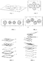
- this embodiment provides a sensor with a time-sharing regional shielding function.
- the touch sensor includes a plurality of sensor units, each of which includes regions contained in four multifunctional layers.
- the four multifunctional layers are arranged in pairs and opposite to each other, and can be arranged at any angle by using the intersection of center connecting lines of the two pairs of multifunctional layers as a center.
- the four multifunctional layers are arranged orthogonally, i.e., at 90 degrees.
- the four multifunctional layers are arranged horizontally, i.e., at 0 degree.
- the four multifunctional layers are arranged at 45 degrees.
- the region contained in each of the multifunctional layers includes an upper portion 11 and a bottom portion corresponding to the multifunctional layer.
- the upper portion 11 is made of a flexible insulating material, and a protective layer 12 made of a flexible insulating material is arranged outside the flexible conducting material.
- the bottom portion includes multiple layers of PCB or FPC boards.
- a flexible insulating layer 17 is arranged below the PCB or FPC boards, a ground-shielding layer 18 controlled by an analog switch is arranged below the flexible insulating layer 17, and an insulating protective layer 19 is arranged below the ground-shielding layer 18 controlled by the analog switch.
- Annular electrodes 141 corresponding to the multifunctional layers are arranged on the PCB or FPC boards 14 in the first layer, circular electrodes 151 are arranged on the PCB or FPC boards 15 in the second layer, and vias 152 are formed on the circular electrodes 151.
- the vias 152 are used for connecting the annular electrodes 141 and the circular electrodes 151 to form independent conducting regions.
- the upper portions 11 made of the flexible conducting material and the PCB or FPC boards 15 in the second layer form complete multifunctional layers. Since the PCB or FPC boards in a single layer have a thickness of 0.025 mm, the requirements of using the multifunctional layers as shielding layers can be completely satisfied.
- Electronic devices of the touch sensor units are arranged on lower surfaces 162 of the PCB or FPC boards 16 in the third layer, and the upper surfaces 161 and lower surfaces 162 of the PCB or FPC boards 16 in the third layer are used for electronic circuit wiring.
- a flexible insulating material 13 is filled in the region corresponding to each of the multifunctional layers, and the flexible insulating material 13 insulate the electrodes in upper and lower layers and the multifunctional layers from each other.
- Cross common electrodes 6 in the upper layer are electrically connected to the PCB or FPC boards in the first layer through central conducting columns 20 arranged in the multifunctional layers.
- Separate electrodes 7 in the lower layer are directly arranged on the PCB or FPC boards 141 in the first layer. The distance from the cross common electrodes in the upper layer to the separate electrodes in the lower layer is 0.5 mm to 3 mm.
- the sensor units each have a volume of 1 mm 3 to 100 mm 3 .
- the ground-shielding layer 18 controlled by the analog switch is made of an organosilicone conductive silver adhesive material
- the insulating protective layer 19 is made of a PDMS material.
- the flexible conducting material is an organic conductive silver adhesive material, and the organic conductive silver adhesive material is bonded to the multifunctional layer through a conductive silver adhesive.
- the upper portions 11 and the bottom portions of the multifunctional layers are bonded or crimped by a conductive adhesive to form electrical connections; and, the conducting columns 20 are electrically connected to the PCB or FPC boards 141 in the first layer by welding, crimping or a conductive adhesive.
- the first multifunctional layer 1 and the third multifunctional layer 3 form a capacitor C1
- the second multifunctional layer 2 and the fourth multifunctional layer 4 form a capacitor C2
- the long dashed lines represent the electric field distribution of the capacitor C1
- the short dashed lines represent the electric field distribution of the capacitor C2.
- the first multifunctional layer 1 and the third multifunctional layer 3 are higher than the second multifunctional layer 2 and the fourth multifunctional layer 4, and the distance from the center of the first multifunctional layer 1 to the center of the third multifunctional layer 3 is greater than the distance from the center of the second multifunctional layer 2 to the center of the fourth multifunctional layer 4.
- an electric field line distribution region of the capacitor C1 is higher than an electric field line distribution region of the capacitor C2.
- the medium in the electric field line distribution regions of both the capacitors C1 and C2 is air, and the capacitance of both the capacitors C1 and C2 will proportionally change with the change in environment temperature and humidity.
- This proportional change is characterized in that the influence from the change in environment temperature and humidity can be eliminated by a digital differential algorithm.
- a digital differential algorithm As shown in Fig. 9 , when the object 5 is within the electric field line distribution region of the capacitor C1 but is not within the electric field line distribution region of the capacitor C2, due to different dielectric constants of objects made of different materials, the capacitance of the capacitor C1 will change, and the change in capacitance of the capacitor C1 is approximately proportional to the dielectric constant of the object, and the capacitance of the capacitor C2 remains unchanged.
- Fig. 9 when the object 5 is within the electric field line distribution region of the capacitor C1 but is not within the electric field line distribution region of the capacitor C2, due to different dielectric constants of objects made of different materials, the capacitance of the capacitor C1 will change, and the change in capacitance of the capacitor C1 is approximately proportional to the dielectric constant of the object, and the capacitance of the capacitor C2 remains unchanged.
- Fig. 9 when the object 5 is
- the change in capacitance of the capacitors C1 and C2 is proportional to the dielectric constant of the object, and the dielectric constant of the object and the approaching distance and speed can be calculated according to the relationship between the change of the capacitors C1 and C2 and the time, so that the functions of classifying and recognizing the object 5 and determining the proximity are realized.
- the bottom portions of the multifunctional layers arranged in the sensor units are arranged in a same plane, so the capacitors provided in this embodiment can be regarded as plane-like capacitors.
- the function of matrix scanning of the sensor while shielding regionally can be realized by the synchronous control by the analog switches and the bus, so that the crosstalk between adjacent sensor units is avoided during the matrix scanning.
- Fig. 13 The capacitive matrix scanning in the prior art is shown in Fig. 13 , where row scanning lines are connected to excitation signals through multiple switches and column scanning lines are connected to a capacitance input measurement channel through multiple switches.
- a certain row and a certain column e.g., the second row and the second column
- the excitation signal in the selected row is simultaneously applied to excitation electrodes for capacitors in all columns, and only the capacitance input stage in the selected column is connected to the capacitance measurement channel.
- excitation electrodes for capacitors in adjacent unselected columns in the selected row will cause crosstalk to the selected capacitor.
- excitation signals on connecting lines in the selected row will cause crosstalk to the selected capacitor.
- An SPI bus selects, by an address bit, a sensor unit in a measurement state and marks this sensor unit as O; and sensor units, for which no address bit is assigned, are marked as X for ground-shielding and thus will not cause crosstalk to the selected sensor unit.
- the selected sensor unit its four multifunctional layers form two plane-like capacitors used to realize touch sensing, and the excitation signal comes from this sensor unit.
- a sensor unit is used as a ground-shielded unit, its four multifunctional layers in this sensor unit are all grounded, and the size of the shielded region (i.e., the number of the ground-shielded units) can be determined according to actual needs.
- the multifunctional layers in this sensor unit temporarily lose their touch sensing function, but the unit for measuring a three-dimensional force in each of the multifunctional layers still operates normally to ensure the stress sensing and slide sensing functions. Since the four multifunctional layers in an unselected sensor unit are all grounded, no crosstalk will be caused to the selected adjacent units.
- the detection units for detecting a three-dimensional force in the multifunctional layers are parallel-plate capacitors.
- the parallel-plate capacitors in the four multifunctional layers in each sensor unit are the same in structure. To simplify the description, the description will be given by taking the internal structure of only the first multifunctional layer 1 as an example.
- four parallel-plate capacitors C3, C4, C5 and C6 are formed by the cross common electrodes 6 in the upper layer of the first multifunctional layer 1 and the four corresponding rectangular separate electrodes 7 in the lower layer, respectively;
- four parallel-plate capacitors C7, C8, C9 and C10 are formed by the cross common electrodes 6 in the upper layer of the second multifunctional layer 2 and the four corresponding rectangular separate electrodes 7 in the lower layer, respectively;
- four parallel-plate capacitors C11, C12, C13 and C14 are formed by the cross common electrodes 6 in the upper layer of the third multifunctional layer 3 and the four corresponding rectangular separate electrodes 7 in the lower layer, respectively;
- four parallel-plate capacitors C15, C16, C17 and C18 are formed by the cross common electrodes 6 in the upper layer of the fourth multifunctional layer 4 and the four corresponding rectangular separate electrodes 7 in the lower layer, respectively, where the common electrodes 6 are connected to excitation signals, and the rectangular electrodes 7 are connected to four capac
- the parallel-plate capacitor C4 and the parallel-plate capacitor C5 have equal capacitance.
- both the distance a1 between two polar plates of the parallel-plate capacitor C4 and the distance a2 between two polar plates of the parallel-plate capacitor C5 change, so that both the capacitance of the parallel-plate capacitor C4 and the capacitance of the parallel-plate capacitor C5 change.
- the magnitude and direction of the applied normal force can be measured.
- the facing area s1 between two polar plates of the parallel-plate capacitor C4 and the facing area s2 between two polar plates of the parallel-plate capacitor C5 change, so that both the capacitance of the parallel-plate capacitor C4 and the capacitance of the parallel-plate capacitor C5 change.
- the magnitude of the applied tangential force can be measured.
- the direction of the applied tangential force can be determined according to different changes in capacitance of the parallel-plate capacitor C4 and the parallel-plate capacitor C5. Specifically, when a tangential force in the direction shown by the arrow in Fig 19 is applied, the absolute value of the change in capacitance of the parallel-plate capacitor C4 is greater than the absolute value of the change in capacitance of the parallel-plate capacitor C5. When a tangential force in a direction opposite to the direction shown by the arrow in Fig 19 is applied, the absolute value of the change in capacitance of the parallel-plate capacitor C4 is less than the absolute value of the change in capacitance of the parallel-plate capacitor C5.
- the direction of the tangential force applied on the sensor can be determined according to different changes in capacitance of the parallel-plate capacitor C4 and the parallel-plate capacitor C5 in this embodiment.
- a sliding force is applied, as shown in Fig. 20 , the normal force and tangential force applied on the parallel-plate capacitor C4 and the parallel-plate capacitor C5 vibrate, so that the distance a1 between two polar plates of the parallel-plate capacitor C4 and the distance a2 between two polar plates of the parallel-plate capacitor C5 as well as the facing area s1 between two polar plates of the parallel-plate capacitor C4 and the facing area s2 between two polar plates of the parallel-plate capacitor C5 all change, resulting in the fluctuation of the capacitance of the parallel-plate capacitor C4 and the capacitance of the parallel-plate capacitor C5.
- the sliding speed and direction can be measured.
- the multifunctional layers cover the cross common electrodes in the upper layer and the separate electrodes in the lower layer, and the multifunctional layers are groove-shaped.
- the multifunctional layers may be hemispherical, elliptic or the like.
- the multifunctional layers are used for electromagnetically shielding the parallel-plate capacitors in the multifunctional layers.
- the electromagnetic shielding is realized in two ways, i.e., ground-shielding and equipotential shielding.
- the multifunctional layers can be grounded by switching the analog switches for the multifunctional layers to a grounded position, to realize the ground-shielding of external electromagnetic signals.
- the multifunctional layers and the common electrodes of the parallel-plate capacitors become equipotential by switching the analog switches for the multifunctional layers to be connected to corresponding excitation signals for the common electrodes for the parallel-plate capacitors, to realize the equipotential shielding of external electromagnetic signals.
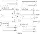
- the multifunctional layers are connected to a processor through analog switches, and the processor is connected to an external circuit through a bus.
- the multifunctional layers regionally shield the functions of the sensor through the time-sharing switching of the analog switches and the control of the bus.
- a sensor unit in a scanning state executes operations in the following period T, where one measurement period T consists of two sub-periods T1 and T2.
- the analog switch K1 for the first multifunctional layer 1 is connected to an excitation signal S1 for the multifunctional layer; the analog switch K3 for the third multifunctional layer 3 is connected to an analog-to-digital conversion circuit M1; and the analog switch K2 for the second multifunctional layer 2 and the analog switch K4 for the fourth multifunctional layer 4 are both grounded, or, the analog switch K2 for the second multifunctional layer 2 is connected to an excitation signal S2-1 for the common electrode 6 of the parallel-plate capacitor in this multifunctional layer and the analog switch K4 for the fourth multifunctional layer 4 is connected to an excitation signal S4-1 for the common electrode 6 of the parallel-plate capacitor in this multifunctional layer.
- the analog switch K1-1 for the parallel-plate capacitor in the first multifunctional layer 1 and the analog switch K3-1 for the parallel-plate capacitor in the third multifunctional layer 3 are both turned off, so that the plane-like capacitor C1 is free of external crosstalk from the second multifunctional layer 2 and the fourth multifunctional layer 4 and free of crosstalk from the parallel-plate capacitors in the first multifunctional layer 1 and the third multifunctional layer 3 when realizing touch sensing.
- the analog switch K2-1 that controls the parallel-plate capacitor in the second multifunctional layer 2 is connected to an excitation signal S2-1 for the common electrode 6 of the parallel-plate capacitor in this multifunctional layer
- the analog switch K4-1 that controls the parallel-plate capacitor in the fourth multifunctional layer 4 is connected to an excitation signal S4-1 for the common electrode 6 of the parallel-plate capacitor in this multifunctional layer, so that the parallel-plate capacitors in the second multifunctional layer 2 and the fourth multifunctional layer 4 can still operate to measure the change in three-dimensional force when the second multifunctional layer 2 an the fourth multifunctional layer 4 are in the shielded state.
- the analog switch K2 for the second multifunctional layer 2 is connected to an excitation signal S2 for the multifunctional layer; the analog switch K4 for the fourth multifunctional layer 4 is connected to an analog-to-digital conversion circuit M2; and the analog switch K1 for the first multifunctional layer 1 and the analog switch K3 for the third multifunctional layer 3 are both grounded, or, the analog switch K1 for the first multifunctional layer 1 is connected to an excitation signal S1-1 for the common electrode 6 of the parallel-plate capacitor in this multifunctional layer and the analog switch K3 for the third multifunctional layer 3 is connected to an excitation signal S3-1 for the common electrode 6 of the parallel-plate capacitor in this multifunctional layer.
- the analog switch K2-1 for the parallel-plate capacitor in the second multifunctional layer and the analog switch K4-1 for the parallel-plate capacitor in the fourth multifunctional layer are both turned off, so that the plane-like capacitor C2 is free of external crosstalk from the first multifunctional layer 1 and the third multifunctional layer 3 and free of crosstalk from the parallel-plate capacitors in the second multifunctional layer 2 and the fourth multifunctional layer 4 when realizing touch sensing.
- the analog switch K1-1 that controls the parallel-plate capacitor in the first multifunctional layer 1 is connected to an excitation signal S1-1 for the common electrode 6 of the parallel-plate capacitor in this multifunctional layer
- the analog switch K3-1 that controls the parallel-plate capacitor in the third multifunctional layer 3 is connected to an excitation signal S3-1 for the common electrode 6 of the parallel-plate capacitor in this multifunctional layer, so that the parallel-plate capacitors in the first multifunctional layer 1 and the third multifunctional layer 3 can still operate to measure the change in three-dimensional force when the first multifunctional layer 1 and the third multifunctional layer 3 are in the shielded state.
- the analog switches K1, K2, K3 and K4 for the four multifunctional layers of the sensor unit in the shielded state are all grounded, or the analog switches K1, K2, K3 and K4 for the four multifunctional layers are connected to excitation signals S1-1, S2-1, S3-1 and S4-1 for common electrodes 6 of the parallel-plate capacitors in the four multifunctional layers, and the analog switches K1-1, K2-1, K3-1 and K4-1 that control the common electrodes of the parallel-plate capacitors in the four multifunctional layers are connected to corresponding excitation signals S1-1, S2-1, S3-1 and S4-1 for the common electrodes 6 of the parallel-plate capacitors, so that the sensor unit in the shielded state can measure the change in three-dimensional force.
- the capacitance is measured by the 7150 chip from the adl Company
- the processor is a 32-bit process with an ARM-mO core
- the external communication is realized by an SPI bus.
- temperature sensing can be realized by combining the multifunctional layers and the parallel-plate capacitors.
- the temperature can be directly measured by the parallel-plate capacitors used for measuring the three-dimensional force.
- the change in ambient temperature can lead to the expansion or contraction of the medium between the parallel-plate capacitors and thus change the distance between the parallel-plate capacitors, resulting in the change in capacitance.
- the existing touch sensors cannot distinguish whether the change in capacitance is caused by the stress from the object or by the change in temperature.
- the temperature sensing function of the touch sensors cannot be realized directly by parallel-plate capacitors.
- the multifunctional layers it can be accurately determined whether an object touches the touch sensor.
- the temperature is only one factor that results in the change of the parallel-plate capacitors.
- Figs. 8 and 25 when the ambient temperature rises, the flexible insulating material between the parallel-plate capacitors will be expanded, so that the distance between the parallel-plate capacitors increases and the capacitance of the four parallel-plate capacitors decreases proportionally.
- Fig. 26 when the ambient temperature falls, the flexible insulating material between the parallel-plate capacitors will be contracted, so that the distance between the parallel-plate capacitors decreases and the capacitance of the four parallel-plate capacitors increases proportionally.
- the change in temperature can be calculated according to the change in capacitance.
- the temperature of the object that touches the touch sensor can be calculated according to the change in capacitance of the parallel-plate capacitors in the second multifunctional layer 2 and the fourth multifunctional layer.
- the parallel-plate capacitors have a measurement range of 0.001 pf to 100 pf.
- the distance from the center of the first multifunctional layer 1 to the center of the third multifunctional layer 3 is d1
- the distance from the center of the second multifunctional layer 2 to the center of the fourth multifunctional layer 4 is d2
- the ratio of d1 to d2 is 1.2 to 5
- the height of the first multifunctional layer 1 and the third multifunctional layer 3 is h1
- the height of the second multifunctional layer 2 and the fourth multifunctional layer 4 is h2
- the difference between h1 and h2 is 1 mm to 3 mm.
- the detection units for detecting a three-dimensional force in the multifunctional layers are piezoresistors.
- the structures and functions of the multifunctional layers are the same as those of the multifunctional layers in Embodiment 1.
- the parallel-plate capacitors for measuring the three-dimensional force in the multifunctional layers are replaced with piezoresistors.
- the electrode structures in the multifunctional layers remain unchanged, except that four rectangular flexible piezoresistors 21 are additionally provided between the cross common electrodes 6 in the upper layer and the rectangular separate electrodes 7 in the lower layer.
- the cross common electrodes 6 in the upper layer and the four rectangular separate electrodes in the lower layer are used as two poles of the piezoresistors 21.
- the four piezoresistors 21 are subjected to a same deformation stress.
- a tangential force or a sliding force is applied, the piezoresistors 21 are subjected to different deformation stresses.
- the change in three-dimensional force can be measured according to the change of the four resistors.
- the multifunctional layers cover the cross common electrodes in the upper layer, the piezoresistors and the separate electrodes in the lower layer, and the multifunctional layers are groove-shaped.
- the multifunctional layers may be hemispherical, elliptic or the like.
- temperature sensing can be realized by combining the multifunctional layers and the piezoresistors 21.
- the four piezoresistors for measuring the three-dimensional force in the multifunctional layers will change in resistance due to the change in temperature, so that temperature sensing can be realized.
- the measurement principle is similar to the principle of measuring temperature by parallel-plate capacitors and will not be repeated here.
- the piezoresistors 21 are made of a conducting rubber piezoresistive material.
- the force-sensitive conducting rubber piezoresistive material is a high-molecular material obtained by uniformly distributing carbon or other highly conducting particles into an insulating flexible polymer substrate material by particular processes.
- the conductivity of the piezoresistive material depends on the density of the conducting particles in the piezoresistive material.
- the density of conducting particles in the piezoresistive material will change, so that the resistance at two ends of the sensor changes.
- the change in three-dimensional force in the multifunctional layers can be measured according to the change in resistance.
- the multifunctional layers are connected to a processor through analog switches, and the processor is connected to an external circuit through a bus.
- the functions of the multifunctional layers controlled by the analog switches and the piezoresistors in the multifunctional layers are switched periodically in a time-sharing manner.
- One measurement period T consists of two sub-periods T1 and T2.
- the analog switch K1 for the first multifunctional layer 1 connects the first multifunctional layer 1 to an excitation signal S1 for the multifunctional layer
- the analog switch K3 for the third multifunctional layer 3 connects the third multifunctional layer 3 to a capacitive analog-to-digital conversion circuit m1, so that the first multifunctional layer 1 and the third multifunctional layer 3 form a plane-like capacitor C1.
- the analog switch K2 for the second multifunctional layer 2 and the analog switch K4 for the fourth multifunctional layer 4 are both grounded.
- the analog switch K1-1 that controls the piezoresistor 21 in the first multifunctional layer 1 and the analog switch K3-1 that controls the piezoresistor 21 in the third multifunctional layer 3 are both turned on, so that the plane-like capacitor C1 is free of external crosstalk from the second multifunctional layer 2 and the fourth multifunctional layer 4 and free of crosstalk from the first multifunctional layer 1 and the third multifunctional layer 3 when realizing touch sensing.
- analog switch K2-1 that controls the piezoresistor 21 in the second multifunctional layer 2 and the analog switch K4-1 that controls the piezoresistor 21 in the fourth multifunctional layer 4 are connected to the common electrodes 6 of the piezoresistors 21 in the two multifunctional layers, so that the piezoresistors 21 in the second multifunctional layer 2 and the fourth multifunctional layer 4 can still operate to measure the change in three-dimensional force when the second multifunctional layer 2 and the fourth multifunctional layer 4 are in the shielded state.
- the analog switch K2 for the second multifunctional layer 2 connects the second multifunctional layer 2 to an excitation signal S2 for the multifunctional layer
- the analog switch K4 for the fourth multifunctional layer 4 connects the fourth multifunctional layer 4 to a capacitive analog-to-digital conversion circuit m2, so that the second multifunctional layer 2 and the fourth multifunctional layer 4 form a plane-like capacitor C2.
- the analog switch K1 for the first multifunctional layer 1 and the analog switch K3 for the third multifunctional layer 3 are both grounded.
- the analog switch K2-1 that controls the piezoresistor 21 in the second multifunctional layer 2 and the analog switch K4-1 that controls the piezoresistor 21 in the fourth multifunctional layer 4 are both turned on, so that the plane-like capacitor C2 is free of external crosstalk from the first multifunctional layer 1 and the third multifunctional layer 3 and free of crosstalk from the second multifunctional layer 2 and the fourth multifunctional layer 4 when realizing touch sensing.
- analog switch K1-1 that controls the piezoresistor 21 in the first multifunctional layer 1 and the analog switch K3-1 that controls the piezoresistor 21 in the third multifunctional layer 3 are connected to the common electrodes 6 of the piezoresistors 21 in the two multifunctional layers, so that the piezoresistors 21 in the first multifunctional layer 1 and the third multifunctional layer 3 can still operate to measure the change in three-dimensional force when the first multifunctional layer 1 and the third multifunctional layer 3 are in the shielded state.
- a selected sensor unit in a measurement state executes the period T, and a sensor unit selected as a shielded region executes a special period T3.
- Analog switches K1, K2, K3 and K4 for four multifunctional layers of a sensor unit in the shielded state are all grounded, and analog switches K1-1, K2-1, K3-1 and K4-1 that control piezoresistors 21 in the four multifunctional layers are connected to cross common electrodes 6 of the piezoresistors 21 in the four multifunctional layers, so that the sensor unit in the shielded state can measure the change in three-dimensional force.
- the capacitance is measured by the 7150 chip from the adl Company
- the processor is a 32-bit process with an ARM-mO core
- the external communication is realized by an SPI bus.
- Another aspect of the present application further relates to electronic skin including the sensor with a time-sharing regional shielding function described above. Since the improvements merely involve the sensor on the artificial skin, other components can be those well-known in the prior art. Therefore, other components of the electronic skin will not be described in the present application.
- Still another aspect of the present application further relates to an intelligent robot including the electronic skin. Since the improvements merely involve the touch sensor on the electronic skin, other components can be those well-known in the prior art. Therefore, other components of the intelligent robot will not be described in the present application.
- Yet another aspect of the present application further relates to an artificial prosthesis including the electronic skin. Since the improvements merely involve the touch sensor on the electronic skin, other components can be those well-known in the prior art. Therefore, other components of the artificial prosthesis will not be described in the present application.
Landscapes
- Engineering & Computer Science (AREA)
- Physics & Mathematics (AREA)
- General Physics & Mathematics (AREA)
- Power Engineering (AREA)
- Human Computer Interaction (AREA)
- Chemical & Material Sciences (AREA)
- Analytical Chemistry (AREA)
- Mechanical Engineering (AREA)
- Robotics (AREA)
- General Engineering & Computer Science (AREA)
- Theoretical Computer Science (AREA)
- Electromagnetism (AREA)
- Force Measurement Appropriate To Specific Purposes (AREA)
- Measurement Of Length, Angles, Or The Like Using Electric Or Magnetic Means (AREA)
Applications Claiming Priority (2)
| Application Number | Priority Date | Filing Date | Title |
|---|---|---|---|
| CN201810093888.6A CN108195490B (zh) | 2018-01-31 | 2018-01-31 | 具有分时、分区域屏蔽功能的传感器、电子皮肤和机器人 |
| PCT/CN2018/000191 WO2019148306A1 (fr) | 2018-01-31 | 2018-05-23 | Capteur à fonction de blindage fondée sur le temps et les zones, membrane électronique et robot |
Publications (3)
| Publication Number | Publication Date |
|---|---|
| EP3748320A1 true EP3748320A1 (fr) | 2020-12-09 |
| EP3748320A4 EP3748320A4 (fr) | 2021-10-20 |
| EP3748320B1 EP3748320B1 (fr) | 2026-04-08 |
Family
ID=62591376
Family Applications (1)
| Application Number | Title | Priority Date | Filing Date |
|---|---|---|---|
| EP18903940.7A Active EP3748320B1 (fr) | 2018-01-31 | 2018-05-23 | Capteur à fonction de blindage fondée sur le temps et les zones, membrane électronique et robot |
Country Status (5)
| Country | Link |
|---|---|
| US (1) | US11598681B2 (fr) |
| EP (1) | EP3748320B1 (fr) |
| JP (1) | JP7054561B2 (fr) |
| CN (1) | CN108195490B (fr) |
| WO (1) | WO2019148306A1 (fr) |
Cited By (1)
| Publication number | Priority date | Publication date | Assignee | Title |
|---|---|---|---|---|
| LU503405B1 (en) * | 2023-01-31 | 2024-07-31 | Innovationlab Gmbh | Printed Sensor |
Families Citing this family (9)
| Publication number | Priority date | Publication date | Assignee | Title |
|---|---|---|---|---|
| AU2018317495B2 (en) * | 2017-08-14 | 2023-10-05 | Contactile Pty Ltd | Friction-based tactile sensor for measuring grip security |
| CN108461015B (zh) * | 2018-06-29 | 2019-11-22 | 华中科技大学 | 一种用于盲文阅读的三维电触觉表皮电子系统 |
| CN111626278B (zh) * | 2019-02-28 | 2024-04-16 | 京东方科技集团股份有限公司 | 纹路识别装置以及纹路识别装置的操作方法 |
| TWI715318B (zh) * | 2019-11-28 | 2021-01-01 | 原見精機股份有限公司 | 自動化設備及其安全裝置 |
| CN111780896B (zh) * | 2020-05-15 | 2021-09-28 | 北京他山科技有限公司 | 一种地理皮肤 |
| JP2022187868A (ja) * | 2021-06-08 | 2022-12-20 | 本田技研工業株式会社 | 力検出装置 |
| CN114571501B (zh) * | 2022-02-28 | 2024-07-23 | 深圳市越疆科技有限公司 | 电子皮肤、接近感应方法、机械臂和机器人 |
| CN117288234A (zh) * | 2022-06-17 | 2023-12-26 | 商升特公司 | 邻近度传感器和天线 |
| CN118952189A (zh) * | 2024-07-16 | 2024-11-15 | 深圳市华盛控科技有限公司 | 一种具备感应皮肤的防护机器人及感应防护方法 |
Family Cites Families (37)
| Publication number | Priority date | Publication date | Assignee | Title |
|---|---|---|---|---|
| US4621227A (en) * | 1984-02-29 | 1986-11-04 | Borg-Warner Corporation | Measuring system for determining the capacitance ratio of a pair of capacitors |
| US4584625A (en) | 1984-09-11 | 1986-04-22 | Kellogg Nelson R | Capacitive tactile sensor |
| US4555954A (en) * | 1984-12-21 | 1985-12-03 | At&T Technologies, Inc. | Method and apparatus for sensing tactile forces |
| US5431064A (en) | 1992-09-18 | 1995-07-11 | Home Row, Inc. | Transducer array |
| US5469070A (en) * | 1992-10-16 | 1995-11-21 | Rosemount Analytical Inc. | Circuit for measuring source resistance of a sensor |
| DE4243832A1 (de) * | 1992-12-23 | 1994-06-30 | Daimler Benz Ag | Tastsensoranordnung |
| US5940526A (en) | 1997-05-16 | 1999-08-17 | Harris Corporation | Electric field fingerprint sensor having enhanced features and related methods |
| TW546480B (en) * | 2000-03-07 | 2003-08-11 | Sumitomo Metal Ind | Circuit, apparatus and method for inspecting impedance |
| DE10134680A1 (de) * | 2001-07-20 | 2003-02-06 | Endress & Hauser Gmbh & Co Kg | Schaltungsanrdnung für einen kapazitiven Sensor |
| FR2849918B1 (fr) * | 2003-01-10 | 2005-06-17 | Faurecia Sieges Automobile | Systeme de detection capacitif, notamment pour interieur de vehicule automobile. |
| FR2885416B1 (fr) * | 2005-05-07 | 2016-06-10 | Acam Messelectronic Gmbh | Procede et dispositif de mesure de capacites. |
| JP4668836B2 (ja) * | 2006-05-09 | 2011-04-13 | ローム株式会社 | 充電制御回路ならびにそれらを用いた充電回路および電子機器 |
| US8164354B2 (en) * | 2006-11-28 | 2012-04-24 | Process Equipment Co. Of Tipp City | Proximity detection system |
| US20080122454A1 (en) * | 2006-11-29 | 2008-05-29 | Aisin Seiki Kabushiki Kaisha | Capacitance detecting apparatus |
| US7679376B2 (en) | 2007-01-19 | 2010-03-16 | Korea Institute Of Science And Technology | Capacitive sensor for sensing tactile and proximity, and a sensing system using the same |
| WO2009044920A1 (fr) * | 2007-10-04 | 2009-04-09 | Fujikura Ltd. | Capteur de proximité capacitif et procédé de détection de proximité |
| DE102008057823A1 (de) * | 2008-11-18 | 2010-08-19 | Ident Technology Ag | Kapazitives Sensorsystem |
| KR20120073264A (ko) | 2009-09-03 | 2012-07-04 | 코닌클리케 필립스 일렉트로닉스 엔.브이. | 터치 감지 출력 장치 |
| TWI410853B (zh) * | 2010-05-07 | 2013-10-01 | Novatek Microelectronics Corp | 用於觸控裝置之電容量測量裝置 |
| JP5535766B2 (ja) * | 2010-05-27 | 2014-07-02 | ラピスセミコンダクタ株式会社 | タイマー回路 |
| US8688393B2 (en) * | 2010-07-29 | 2014-04-01 | Medtronic, Inc. | Techniques for approximating a difference between two capacitances |
| US20120240691A1 (en) * | 2011-03-23 | 2012-09-27 | University Of Southern California | Elastomeric optical tactile sensor |
| TWI564543B (zh) * | 2011-06-30 | 2017-01-01 | 瑪波微影Ip公司 | 電容測量系統、測量電路以及微影蝕刻機器 |
| US9564275B2 (en) * | 2012-03-09 | 2017-02-07 | The Paper Battery Co. | Supercapacitor structures |
| CN104969158A (zh) * | 2012-12-14 | 2015-10-07 | 苹果公司 | 通过电容变化进行力感测 |
| DE102014115802A1 (de) * | 2014-10-30 | 2016-05-04 | Endress + Hauser Gmbh + Co. Kg | Kapazitiver Drucksensor und Verfahren zu dessen Herstellung |
| DE102016208381A1 (de) * | 2016-05-17 | 2017-11-23 | Robert Bosch Gmbh | Kondensator, insbesondere Zwischenkreiskondensator für ein Mehrphasensystem |
| US10242792B2 (en) * | 2016-05-20 | 2019-03-26 | Murata Manufacturing Co., Ltd. | Multilayer electronic component |
| KR102803440B1 (ko) * | 2016-11-04 | 2025-05-07 | 삼성전기주식회사 | 적층 세라믹 커패시터 |
| CN106706176A (zh) * | 2016-11-23 | 2017-05-24 | 浙江大学 | 具有图案化微结构阵列的电容式触觉传感器 |
| WO2018116706A1 (fr) * | 2016-12-21 | 2018-06-28 | アルプス電気株式会社 | Dispositif de détection de capacité et dispositif d'entrée |
| CN106840476B (zh) * | 2017-01-25 | 2019-12-03 | 东南大学 | 三维碳纳米材料场效应柔性力敏传感元件及制备方法 |
| EP3438677B1 (fr) * | 2017-07-31 | 2024-07-10 | Sciosense B.V. | Procédé de détermination d'un paramètre électrique et agencement de mesure permettant de déterminer un paramètre électrique |
| JP2019113391A (ja) * | 2017-12-22 | 2019-07-11 | ルネサスエレクトロニクス株式会社 | 圧力センサ装置、制御装置、及び、圧力センサユニット |
| WO2019147800A2 (fr) * | 2018-01-24 | 2019-08-01 | Gentherm Inc. | Système de détection et de chauffage capacitif pour des volants ou des sièges pour détecter la présence d'une main d'un occupant sur un volant ou d'un occupant dans un siège |
| CN207923324U (zh) * | 2018-01-31 | 2018-09-28 | 北京他山科技有限公司 | 具有分时、分区域屏蔽功能的传感器、电子皮肤和机器人 |
| JP7119478B2 (ja) * | 2018-03-23 | 2022-08-17 | セイコーエプソン株式会社 | 回路装置、物理量測定装置、電子機器及び移動体 |
-
2018
- 2018-01-31 CN CN201810093888.6A patent/CN108195490B/zh active Active
- 2018-05-23 EP EP18903940.7A patent/EP3748320B1/fr active Active
- 2018-05-23 US US16/966,492 patent/US11598681B2/en active Active
- 2018-05-23 WO PCT/CN2018/000191 patent/WO2019148306A1/fr not_active Ceased
- 2018-05-23 JP JP2020542310A patent/JP7054561B2/ja active Active
Cited By (2)
| Publication number | Priority date | Publication date | Assignee | Title |
|---|---|---|---|---|
| LU503405B1 (en) * | 2023-01-31 | 2024-07-31 | Innovationlab Gmbh | Printed Sensor |
| WO2024160869A1 (fr) | 2023-01-31 | 2024-08-08 | Innovationlab Gmbh | Capteur imprimé |
Also Published As
| Publication number | Publication date |
|---|---|
| CN108195490B (zh) | 2019-10-11 |
| WO2019148306A1 (fr) | 2019-08-08 |
| EP3748320B1 (fr) | 2026-04-08 |
| CN108195490A (zh) | 2018-06-22 |
| JP2021512329A (ja) | 2021-05-13 |
| EP3748320A4 (fr) | 2021-10-20 |
| US20210041309A1 (en) | 2021-02-11 |
| US11598681B2 (en) | 2023-03-07 |
| JP7054561B2 (ja) | 2022-04-14 |
Similar Documents
| Publication | Publication Date | Title |
|---|---|---|
| EP3748321B1 (fr) | Capteur de contact possédant une couche multifonctionnelle, membrane électronique et robot intelligent | |
| EP3748320B1 (fr) | Capteur à fonction de blindage fondée sur le temps et les zones, membrane électronique et robot | |
| CN108446042B (zh) | 一种电容式触摸传感器、电子皮肤和智能机器人 | |
| CN108362428B (zh) | 一种阻容复合式触摸传感器、电子皮肤和智能机器人 | |
| CN104764481B (zh) | 一种全柔性电容‑电阻双模式接近觉传感器 | |
| GB2533667A (en) | Pressure-sensitive touch panel | |
| CN105549791B (zh) | 一种具有压力感应和触控功能的显示面板 | |
| CN207923324U (zh) | 具有分时、分区域屏蔽功能的传感器、电子皮肤和机器人 | |
| CN106383607A (zh) | 具有压力感测的触控显示系统 | |
| CN207741882U (zh) | 一种具有多功能层的接触传感器、电子皮肤和智能机器人 | |
| CN106293188A (zh) | 一种触控面板 | |
| CN113386158B (zh) | 一种全打印仿生超感知柔性机器人皮肤 | |
| CN209820667U (zh) | 一种电容式触摸传感器、电子皮肤和智能机器人 | |
| CN108132113B (zh) | 应用多功能层实现电磁屏蔽的传感器、电子皮肤和机器人 | |
| CN207867477U (zh) | 触摸传感器和电容触摸传感器系统 | |
| CN210036760U (zh) | 双模传感单元和双模传感器 | |
| CN111896163A (zh) | 一种电阻式触摸传感器、电子皮肤和智能机器人 | |
| CN207764769U (zh) | 一种电容式触摸传感器、电子皮肤和智能机器人 | |
| CN207741883U (zh) | 一种阻容复合式触摸传感器、电子皮肤和智能机器人 | |
| CN113176837B (zh) | 三维触控传感器及显示装置 | |
| CN111896165A (zh) | 一种电容式触摸传感器、电子皮肤和智能机器人 | |
| CN207816489U (zh) | 应用多功能层实现电磁屏蔽的传感器、电子皮肤和机器人 | |
| US12492921B2 (en) | Touch sensor | |
| CN206282251U (zh) | 具有压力感测的触控显示系统 | |
| CN209486649U (zh) | 一种具有接近探测功能的电容触摸屏 |
Legal Events
| Date | Code | Title | Description |
|---|---|---|---|
| STAA | Information on the status of an ep patent application or granted ep patent |
Free format text: STATUS: THE INTERNATIONAL PUBLICATION HAS BEEN MADE |
|
| PUAI | Public reference made under article 153(3) epc to a published international application that has entered the european phase |
Free format text: ORIGINAL CODE: 0009012 |
|
| STAA | Information on the status of an ep patent application or granted ep patent |
Free format text: STATUS: REQUEST FOR EXAMINATION WAS MADE |
|
| 17P | Request for examination filed |
Effective date: 20200730 |
|
| AK | Designated contracting states |
Kind code of ref document: A1 Designated state(s): AL AT BE BG CH CY CZ DE DK EE ES FI FR GB GR HR HU IE IS IT LI LT LU LV MC MK MT NL NO PL PT RO RS SE SI SK SM TR |
|
| AX | Request for extension of the european patent |
Extension state: BA ME |
|
| DAV | Request for validation of the european patent (deleted) | ||
| DAX | Request for extension of the european patent (deleted) | ||
| A4 | Supplementary search report drawn up and despatched |
Effective date: 20210921 |
|
| RIC1 | Information provided on ipc code assigned before grant |
Ipc: G01L 19/06 20060101ALI20210915BHEP Ipc: B25J 13/08 20060101ALI20210915BHEP Ipc: G01L 9/12 20060101ALI20210915BHEP Ipc: G01L 5/161 20200101ALI20210915BHEP Ipc: G01L 5/00 20060101ALI20210915BHEP Ipc: G01L 1/20 20060101ALI20210915BHEP Ipc: G06F 3/044 20060101ALI20210915BHEP Ipc: G01L 1/14 20060101AFI20210915BHEP |
|
| STAA | Information on the status of an ep patent application or granted ep patent |
Free format text: STATUS: EXAMINATION IS IN PROGRESS |
|
| 17Q | First examination report despatched |
Effective date: 20230928 |
|
| GRAP | Despatch of communication of intention to grant a patent |
Free format text: ORIGINAL CODE: EPIDOSNIGR1 |
|
| STAA | Information on the status of an ep patent application or granted ep patent |
Free format text: STATUS: GRANT OF PATENT IS INTENDED |
|
| RIC1 | Information provided on ipc code assigned before grant |
Ipc: G01L 1/14 20060101AFI20250923BHEP Ipc: G06F 3/044 20060101ALI20250923BHEP Ipc: G01L 1/20 20060101ALI20250923BHEP Ipc: G01L 5/00 20060101ALI20250923BHEP Ipc: G01L 5/161 20200101ALI20250923BHEP Ipc: G01L 5/165 20200101ALI20250923BHEP Ipc: G01L 9/12 20060101ALI20250923BHEP Ipc: B25J 13/08 20060101ALI20250923BHEP Ipc: G01L 19/06 20060101ALI20250923BHEP |
|
| INTG | Intention to grant announced |
Effective date: 20251015 |
|
| GRAS | Grant fee paid |
Free format text: ORIGINAL CODE: EPIDOSNIGR3 |
|
| GRAA | (expected) grant |
Free format text: ORIGINAL CODE: 0009210 |
|
| STAA | Information on the status of an ep patent application or granted ep patent |
Free format text: STATUS: THE PATENT HAS BEEN GRANTED |
|
| P01 | Opt-out of the competence of the unified patent court (upc) registered |
Free format text: CASE NUMBER: UPC_APP_0004121_3748320/2026 Effective date: 20260204 |
|
| AK | Designated contracting states |
Kind code of ref document: B1 Designated state(s): AL AT BE BG CH CY CZ DE DK EE ES FI FR GB GR HR HU IE IS IT LI LT LU LV MC MK MT NL NO PL PT RO RS SE SI SK SM TR |
|
| RAP3 | Party data changed (applicant data changed or rights of an application transferred) |
Owner name: BEIJING TASHAN TECHNOLOGY CO., LTD. |
|
| REG | Reference to a national code |
Ref country code: CH Ref legal event code: F10 Free format text: ST27 STATUS EVENT CODE: U-0-0-F10-F00 (AS PROVIDED BY THE NATIONAL OFFICE) Effective date: 20260408 Ref country code: GB Ref legal event code: FG4D |
|
| REG | Reference to a national code |
Ref country code: DE Ref legal event code: R096 Ref document number: 602018090489 Country of ref document: DE |