EP3748370B1 - Stromsensoren und entsprechende messsysteme - Google Patents
Stromsensoren und entsprechende messsysteme Download PDFInfo
- Publication number
- EP3748370B1 EP3748370B1 EP20178435.2A EP20178435A EP3748370B1 EP 3748370 B1 EP3748370 B1 EP 3748370B1 EP 20178435 A EP20178435 A EP 20178435A EP 3748370 B1 EP3748370 B1 EP 3748370B1
- Authority
- EP
- European Patent Office
- Prior art keywords
- coil
- current sensor
- substrate
- coils
- holes
- Prior art date
- Legal status (The legal status is an assumption and is not a legal conclusion. Google has not performed a legal analysis and makes no representation as to the accuracy of the status listed.)
- Active
Links
Images


Classifications
-
- G—PHYSICS
- G01—MEASURING; TESTING
- G01R—MEASURING ELECTRIC VARIABLES; MEASURING MAGNETIC VARIABLES
- G01R15/00—Details of measuring arrangements of the types provided for in groups G01R17/00 - G01R29/00, G01R33/00 - G01R33/26 or G01R35/00
- G01R15/14—Adaptations providing voltage or current isolation, e.g. for high-voltage or high-current networks
- G01R15/18—Adaptations providing voltage or current isolation, e.g. for high-voltage or high-current networks using inductive devices, e.g. transformers
- G01R15/181—Adaptations providing voltage or current isolation, e.g. for high-voltage or high-current networks using inductive devices, e.g. transformers using coils without a magnetic core, e.g. Rogowski coils
-
- G—PHYSICS
- G01—MEASURING; TESTING
- G01R—MEASURING ELECTRIC VARIABLES; MEASURING MAGNETIC VARIABLES
- G01R15/00—Details of measuring arrangements of the types provided for in groups G01R17/00 - G01R29/00, G01R33/00 - G01R33/26 or G01R35/00
- G01R15/14—Adaptations providing voltage or current isolation, e.g. for high-voltage or high-current networks
- G01R15/18—Adaptations providing voltage or current isolation, e.g. for high-voltage or high-current networks using inductive devices, e.g. transformers
- G01R15/188—Adaptations providing voltage or current isolation, e.g. for high-voltage or high-current networks using inductive devices, e.g. transformers comprising rotatable parts, e.g. moving coils
-
- G—PHYSICS
- G01—MEASURING; TESTING
- G01R—MEASURING ELECTRIC VARIABLES; MEASURING MAGNETIC VARIABLES
- G01R19/00—Arrangements for measuring currents or voltages or for indicating presence or sign thereof
- G01R19/0092—Measuring current only
-
- H—ELECTRICITY
- H01—ELECTRIC ELEMENTS
- H01F—MAGNETS; INDUCTANCES; TRANSFORMERS; SELECTION OF MATERIALS FOR THEIR MAGNETIC PROPERTIES
- H01F3/00—Cores, Yokes, or armatures
- H01F3/10—Composite arrangements of magnetic circuits
-
- H—ELECTRICITY
- H01—ELECTRIC ELEMENTS
- H01F—MAGNETS; INDUCTANCES; TRANSFORMERS; SELECTION OF MATERIALS FOR THEIR MAGNETIC PROPERTIES
- H01F5/00—Coils
- H01F5/003—Printed circuit coils
-
- H—ELECTRICITY
- H01—ELECTRIC ELEMENTS
- H01F—MAGNETS; INDUCTANCES; TRANSFORMERS; SELECTION OF MATERIALS FOR THEIR MAGNETIC PROPERTIES
- H01F3/00—Cores, Yokes, or armatures
- H01F3/10—Composite arrangements of magnetic circuits
- H01F2003/106—Magnetic circuits using combinations of different magnetic materials
Definitions
- the present invention relates to current sensors and associated measurement systems.
- Rogowski windings are current sensors capable of measuring the intensity of an alternating current flowing in an electrical conductor.
- Such a sensor generally comprises a coil wound around a contour line closed around a central opening in which the electrical conductor is received. The current flowing in the electrical conductor induces an electrical voltage across the coil.
- Rogowski windings can be fabricated on a printed circuit board (PCB).
- PCB printed circuit board
- an insulating substrate is pierced with a plurality of through holes arranged on the faces of the substrate with a predefined pattern along a square-shaped closed contour around a central opening.
- the coil is formed by passing an electrical conductor through the through holes to form turns centered on the contour line.
- Rogowski windings on printed circuit have the particular advantages of being relatively simple and inexpensive to manufacture on an industrial scale. They are also easy to miniaturize.
- Known prior art examples can be seen in documents US 2009/058398 A1 , FR 3 033 647 A1 , US 2008/079418 A1 And US 2019/154733 A1 .
- Rogowski sensors on a printed circuit are low and may be insufficient to be used in certain applications, in particular in applications related to the protection of electricity distribution installations, for example when these sensors are used as current sensors in circuit breaker trip units.
- Such sensors can be subject to crosstalk problems, which can complicate the detection of an electrical fault such as a short-circuit current.
- a measurement system comprises a current sensor as described above and an electronic processing circuit configured to process the signal measured by the current sensor.
- a measurement system 2 is shown for measuring the intensity of an electric current flowing in an electrical conductor 4, such as a cable or a wire or a connection bar.
- System 2 here comprises a current sensor 6 and an electronic processing circuit 8 connected to current sensor 6 and configured to process the signal measured by current sensor 6.
- the current sensor 6 comprises a Rogowski winding formed on a substrate and comprising two coils electrically connected in series, these coils being superposed and wound on the substrate.
- End terminals of the winding are connected to an input of processing circuit 8.
- the current flowing in the electrical conductor induces an electrical voltage across the terminals of the winding. This voltage is proportional to the time derivative of the intensity of the current flowing in the conductor 4.
- the processing circuit 8 is, for example, configured to calculate the value of the current from the voltage signal provided at the output of the sensor of stream 6.
- the current sensor 6 and the processing circuit 8 can be mounted on the same printed circuit support.
- a first embodiment of the current sensor 6 is represented on the figure 2 And 3 .
- the current sensor 6 comprises a substrate 10 that is electrically insulating and preferably has a planar shape.
- the substrate 10 is a printed circuit support comprising a layer or several stacked layers of a hardened polymer material, such as an “FR-4” type epoxy resin.
- the substrate 10 can, for example, be manufactured by lamination, or by deposition of material, or by additive manufacturing, or by any other appropriate process.
- the coils are, for example, formed by winding electrically conductive wires or by depositing metal layers during the manufacture of the substrate 10.
- the current sensor 6 comprises a Rogowski winding 14 surrounding an opening 12 formed on the substrate 10.
- the opening 12 is preferably placed in the central position of the substrate 10.
- opening 12 has a polygon shape, such as a quadrilateral.
- other shapes can be envisaged, such as a circle or an ellipse.
- Winding 14 includes a first coil 16 and a second coil 18 superposed and electrically connected in series.
- the first coil 16 and the second coil 18 are wound around the substrate according to, respectively, a first contour line C1 and a second contour line C2.
- Each contour line C1 and C2 delimits, in the plane of the substrate 10, a contour in the shape of a quadrilateral centered around the central opening.
- the quadrilateral is a rectangle.
- the coils 16 and 18 of the winding 14 are superposed and are interlaced with each other.
- interlaced means that, over at least part of the length of the closed contour, the respective turns of the coils 16 and 18 are arranged alternately.
- said coils 16 and 18 are offset relative to each other in a direction perpendicular to the plane of substrate 10.
- each coil 16, 18 has an upper face and a lower face which extend in geometric planes parallel to the plane of the substrate 10.
- the electrical conductors forming the coils 16 and 18 then extend between the upper and lower faces. by crossing at least part of the thickness of the substrate 10 by means of through holes oriented in directions perpendicular to the plane of the substrate 10, such as vias drilled in the substrate 10.
- the upper face of coil 18 is disposed on the upper face of substrate 10.
- the lower face of coil 18 is disposed in a first internal layer in substrate 10.
- the upper face of coil 16 is disposed in a second internal layer in the substrate 10 and its lower face is arranged on the lower face of the substrate 10, the second internal layer here being located between the upper face of the substrate 10 and the first internal layer.
- the figure 2 represents a view of the upper face of the substrate 10.
- the electrical conductors of the coil 18 are represented in fine lines, and only the electrical conductors of the coil 16 which are located at the level of the internal layer are represented in solid lines, those arranged on the underside of the substrate 10 not being drawn to facilitate reading of the figure.
- each of the coils 16 and 18 is divided into a plurality of coil parts of rectilinear shape arranged around the opening 12. These coil parts, also called coil segments in the following, are arranged so as to delimit a quadrilateral around the opening 12 and are substantially aligned along the contour lines C1 and C2.
- the coil segments are not necessarily rectilinear and may have a rounded or arcuate shape.
- each coil segment 20, 22, 24 and 26 are arranged end to end at right angles around the opening 12, parallel to the plane of the substrate 10, so as to form a square or a rectangle around the opening 12.
- the segments 20 and 24 are parallel and face each other on either side of the opening 12.
- the segments 22 and 26 are arranged face to face on either side of the opening 12 and are oriented perpendicular to segments 20 and 24.
- Coils 16 and 18 also include corner zones 28, 30, 32 and 34 each arranged in the corner between two adjacent coil segments.
- the electrical conductors of the coils 16 and 18 pass through these corner zones to connect the coil segments two by two.
- corner zone 28 is adjacent to coil segments 20 and 22;
- corner zone 30 is adjacent to coil segments 22 and 24, and so on.
- each coil 16, 18 is wound in a plurality of turns which are at least partly formed by through holes drilled in the substrate, the through holes being aligned along of rows 36, 38, 40, 42.
- first row 36 is closer to aperture 12 than second row 38, while for coil portions 22 and 24, second row 38 is closer to aperture 12 than the first row 26.
- the conductors of the coil 18 extend between a third row 40 of through holes and a fourth row 42 of through holes.
- third row 40 is closer to opening 12 than fourth row 42
- fourth row 42 is closer to opening 12 than the third row 40.
- first row ports 36 are staggered with third row ports 40.
- Second row ports 38 are staggered with fourth row ports 42.
- the lower faces of the coils 18 and 16 are arranged in an analogous manner, respectively, on the lower face of the substrate 10 and in the first internal layer.
- the quadrilateral-shaped contour delimited by the first contour line C1 has a length L1 greater than the length L2 of the quadrilateral delimited by the second contour line C2 and a width l1 less than the width l2 of the quadrilateral delimited by the second line of outline C2.
- This arrangement provides sensor 6 with better immunity against crosstalk phenomena, in particular when the winding is subjected to a uniform magnetic field. Indeed, the superposition of the two coils with surfaces equivalent but whose directions are opposite eliminates the uniform field contribution perpendicular to the sensor. The quality of the measurement is therefore improved.
- each contour C1 and C2 comprises a protrusion, denoted E1 and E2 respectively, which makes it possible to connect the coils to the processing circuit 8.
- the protrusions E1 and E2 are superimposed.
- the orifices are arranged with regular spacing and, preferably, are aligned in a straight line.
- the rows are not necessarily rectilinear, as will be seen in the example of the picture 3 .
- Coils 16 and 18 are interleaved such that for each coil segment 20, 22, 24 and 26, the first row holes 36 are aligned with the fourth row holes 42 and the second row holes 38 are aligned with the holes in the third row 40.
- a similar pattern can be used for the corner zones 28, 30, 32 and 34.
- holes for the conductor of the coil 18 are aligned along two parallel rows located in the extension of rows 38 and 40 of the coil part 20.
- Holes for receiving the conductor of the coil 16 are aligned along two parallel rows located in the extension of the rows 36 and 42 of the coil part 22.
- the corner parts 30, 32 and 34 are constructed analogously.
- the turns of the winding have a pattern taking into account the staggered arrangement of the orifices.
- the coil 16 comprises a pattern by which, in the upper face of the coil, the electrical conductor forming the coil 16 comprises a first rectilinear part which extends from the row 40 in the direction of the opposite row 42 parallel to the plane of the substrate 10 and perpendicular to said row 40.
- the first rectilinear part is extended by a second rectilinear part oriented diagonally and itself extended by a third rectilinear part parallel to the first rectilinear part.
- These second and third parts are parallel to the plane of the substrate 10 and are coplanar with the first rectilinear part.
- This diagonal part makes it possible to laterally shift the electrical conductor so that it is opposite the corresponding orifice of row 42, instead to be opposite one of the orifices of the row 38 provided for the second coil 18.
- the length of the third part is similar or equal to that of the first part.
- the conductor then extends towards the underside of the coil 18 by descending through said orifice. Once this opposite face has been reached, the conductor extends from row 42 towards row 40 along a similar fourth rectilinear part superimposed with the third rectilinear part.
- the fourth part is extended by a fifth rectilinear part oriented diagonally, analogously to the second part except that it is inclined towards the opposite side.
- the fifth part has a length equal or substantially equal (that is to say preferably less than or equal to 10%) to the length of the second part.
- This fifth part is itself extended towards a corresponding orifice of row 40 by a sixth rectilinear part parallel to the fourth rectilinear part.
- These fifth and sixth parts are parallel to the plane of the substrate 10 and are coplanar with the fourth rectilinear part.
- the conductor then rises to the upper face of the coil 18 and the same pattern is reproduced as described above.
- the coil 16 has a similar pattern along the straight portions, except that it is offset from that of the first coil, due to the staggered arrangement of the orifices along the rows 36 and 40 and the rows 38 and 42. Such a pattern is not completely visible on the figure 1 , which does not show the arrangement of the conductor in the lower part of the coil 16 for reasons of clarity. On the other hand, a similar pattern is clearly visible on the figure 5 described below with reference to the coil 504.
- the conductor of the coil 504 comprises rectilinear parts similar to those of the conductor of the coil 18.
- the diagonally oriented parts are also offset laterally with respect to those of the conductor of the coil 18 while being arranged vertically thereto, for example by being aligned therewith along a covering strip which extends parallel to the rows 36, 38, 40 and 42, for example located halfway between rows 36 and 42.
- each turn comprises, in the upper and lower faces of the coil, a rectilinear portion oriented diagonally, the rectilinear portions of the coils being, in each coil segment, aligned along a covering strip s' extending parallel to said rows 36, 38, 40 and 42.
- This arrangement makes it possible to obtain a compact winding with a high density of turns, which improves the performance of sensor 6.
- Similar patterns can be used for the corner areas 28, 30, 32 and 34, except that the conductors of the coil 16 are not arranged parallel to that of the coil 18, but on the contrary are oriented perpendicular to it. in the plane of the substrate 10.
- the rows are not necessarily rectilinear and can follow rounded contours, for example in an arc of a circle.
- This non-rectilinear arrangement may be useful for optimizing the arrangement of the orifices and thus saving space on the substrate 10.
- the alignment of the orifices may only be partially rectilinear, that is to say that at least part of the holes (for example up to 20% or 40% or 60% of the holes) of the row are misaligned.
- FIG 5 represents an embodiment of the invention which can be combined with the embodiments of the figure 2 And 3 or, alternatively, be implemented independently of these embodiments.
- a portion of a sensor 400 similar to sensor 6 is shown in a sectional view in a geometric plane perpendicular to the plane of substrate 10.
- the substrate 10 comprises a layer 402 covered by a lower layer 404 and an upper layer 405.
- the sensor 400 comprises a Rogowski winding including coils playing a role similar to the coils 16 and 18 but which, in addition, are nested within the substrate 10.
- first through vias 406, 408 which each extend, in a direction perpendicular to the plane of the substrate 10, between an upper end 410 formed at the junction between the layers 405 and 402, and an end 412 formed on the lower layer 404.
- the first vias 406, 408 are, for example, associated with the second coil 18 of the winding.
- a plurality of second through vias 414 each extend, in a direction perpendicular to the plane of the substrate 10, between a lower end 416 at the junction between the layers 404 and 402, and an upper end 418 formed on the layer 405.
- the second vias 414 are, for example , associated with the first coil 16 of the winding.
- the substrate 10 can be more easily structured to nest the coils of the winding.
- the manufacturing process is simplified, because only one metallization step is necessary, unlike substrates formed by stacking layers and in which blind vias open into an intermediate layer of the stack, which require at least three steps. distinct from metallization, which increases the cost and complexity of the manufacturing process.
- a sensor 500 similar to the sensor 6 previously described comprises a winding 502 including a first coil 504 and a second coil 506 wound on a substrate provided with an opening 508.
- the coils 504 and 506 comprise coil segments 510, 512, 514 and 516 similar to coil portions 20-26 previously described.
- the sensor 500 differs in particular from the sensor 6 in that it comprises at least one connection zone 518 formed in one of the coil parts to allow electrical connection of the winding to the processing circuit 8.
- connection zone 518 comprises contact pads to which are connected a terminal end of each of the coils 504 and 506.
- the connection zone 518 is formed at mid-width of the part of the coil 514.
- connection zone 518 comprises additional through-holes.
- these additional through-holes are formed at the level of the rows of holes (similar to rows 38 and 42 previously described) located near the edge of the substrate 10. Said additional through-holes are arranged according to a predefined pattern.
- a similar pattern 520 (but not necessarily including said additional through-holes) is placed on the coil segment 510 symmetrically with respect to the connection zone 518.
- the coils can therefore be easily connected to a measurement circuit external to the sensor 500 without having to introduce sensor anisotropic behavior.
- additional patterns 522 and 524 of similar shape are arranged symmetrically on the other coil segments 512 and 514.
- FIG. 6 And 7 show other embodiments of sensor 6 or sensor 500.
- a sensor 600 similar to the sensor 6 previously described and which comprises a winding 602 including a first coil 604 and a second coil 606 wound on a substrate provided with an opening 608.
- the coils 604 and 606 comprise coil segments 610, 612, 614 and 616 similar to the parts of coils 20 to 26 previously described.
- the sensor 600 differs in particular from the sensor 6 in that metal pads 618 are arranged on the substrate 10, for example on the upper face of the substrate 10.
- the pads 618 form weld pads to ensure a welded assembly, having good mechanical, of at least two sensors.
- the pads 618 have for example a rectangular shape.
- the metal pads 618 are arranged on locations aligned with the turns of one of the coils of the winding, for example with the coil 606. In the example illustrated, these locations are located in the coil segments 610, 612, 614 and 618 vertically above the turns of coil 606, preferably above the turns of coil 606.
- top side of coil 606 extends into one of the inner layers in substrate 10 below the top side of substrate 10, plates 618 are not in contact with coil 606. Plates 618 are further dimensioned not to be in contact with the coil 604 and are thus electrically isolated from the winding 602.
- This arrangement makes it possible to maintain a compact winding with a high density of turns.
- each plate 618 is placed halfway between the rows of orifices 36 and 42.
- the shape of the turns of the coils 604 and 606 can be modified, for example by shifting the diagonal parts of the conductors towards the one of rows 36 or 42, as shown in the figure 6 .
- the shape of the rows 36, 38, 40 or 42 can then be locally modified so as to no longer present a rectilinear alignment.
- the alignment may be partially straight, i.e. at least some of the holes (eg up to 20% or 40% or 60% of the holes) in the row are misaligned.
- a sensor 700 similar to sensor 7 and which comprises a winding 702 including a first coil 704 and a second coil 706 wound on a substrate provided with an opening 708.
- the coils 704 and 706 comprise coil segments 710, 712, 714 and 716 similar to coil segments 610, 612, 614 and 616.
- Sensor 700 also has reinforcement plates similar to plates 618 but which are not visible on the figure 7 .
- the sensor 700 differs in particular from the sensor 600 in that the shape of some of the rows can be modified, for example by following a curved shape in an arc of a circle, as illustrated by way of example by the dotted line bearing the reference 718. Corner areas of coils 704 and 706 can also be modified to accommodate reinforcement plates similar to plates 618.
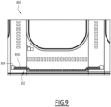
- the sensor 800 comprises, on at least part of the substrate, a shielding structure 802 to protect the sensor against electromagnetic disturbances.
- the structure 802 is arranged on an edge of the substrate to avoid electromagnetic coupling of the winding with the power supply of the measurement system 2.
- the structure 802 comprises an electrically conductive track 804 connected to an electrical ground, for example to an electrical ground of the system 2, this track 804 being deposited on one face of the substrate.
- holes 806 are drilled in the substrate along track 804.
Landscapes
- Engineering & Computer Science (AREA)
- Power Engineering (AREA)
- Physics & Mathematics (AREA)
- General Physics & Mathematics (AREA)
- Chemical & Material Sciences (AREA)
- Composite Materials (AREA)
- Measuring Instrument Details And Bridges, And Automatic Balancing Devices (AREA)
Claims (10)
- Stromsensor (6), umfassend:- ein isolierendes Substrat (10), das mit einer mittleren Öffnung (12) versehen ist;- eine Rogowski-Wicklung (14), die die mittlere Öffnung umgibt und eine erste Spule (16) und eine zweite Spule (18) beinhaltet, die übereinander angeordnet und elektrisch in Reihe geschaltet sind, wobei die erste Spule und die zweite Spule entlang einer ersten Konturlinie (C1) bzw. einer zweiten Konturlinie (C2) um das Substrat gewickelt sind, wobei jede Konturlinie in der Ebene des Substrats eine Kontur in Form eines Vierecks begrenzt, das um die mittlere Öffnung zentriert ist;dadurch gekennzeichnet, dass die viereckige Kontur, die durch die erste Konturlinie (C1) begrenzt ist, eine Länge (L1) aufweist, die größer ist als die Länge (L2) des Vierecks, das durch die zweite Konturlinie (C2) begrenzt ist, und eine Breite (ℓ1), die kleiner ist als die Breite (Q2) des Vierecks, das durch die zweite Konturlinie (C2) begrenzt ist.
- Stromsensor nach Anspruch 1, wobei jede der Spulen (16, 18) in eine Vielzahl von Spulensegmenten (20, 22, 24, 26) unterteilt ist, die um die mittlere Öffnung angeordnet sind, indem sie übereinander liegen und im Wesentlichen entlang von Konturlinien (C1, C2) ausgerichtet sind, wobei jedes der Segmente (20, 22, 24, 26) eine Vielzahl von Windungen aufweist, die zumindest teilweise in Durchgangslöchern aufgenommen sind, die in das Substrat gebohrt sind, wobei die Durchgangslöcher entlang von Reihen (36, 38, 40, 42) ausgerichtet sind.
- Stromsensor nach Anspruch 2, wobei die Öffnungen, die mit der ersten und der zweiten Spule assoziiert sind, für jeden Spulenteil versetzt angeordnet sind.
- Stromsensor nach Anspruch 3, wobei jede Windung in der Ober- und der Unterseite der Spule einen diagonal ausgerichteten geraden Abschnitt aufweist, wobei die geraden Abschnitte der Spulen in jedem Spulensegment entlang eines sich parallel zu den genannten Reihen (36, 38, 40, 42) erstreckenden Abdeckstreifens ausgerichtet sind.
- Stromsensor nach einem der Ansprüche 2 bis 4, wobei der Stromsensor (500) einen Anschlussbereich (518) umfasst, der in einem der Spulensegmente gebildet ist, wobei der Anschlussbereich Durchgangslöcher umfasst, die in einem vorbestimmten Muster angeordnet sind, der Stromsensor (500) ferner umfassend zusätzliche Durchgangsöffnungen (520, 522, 524), die in demselben Muster angeordnet sind und in einem anderen der Spulensegmente symmetrisch in Bezug auf den Anschlussbereich angeordnet sind
- Stromsensor nach einem der Ansprüche 2 bis 5, wobei die Durchgangslöcher Durchkontaktierungen (404, 406, 414) sind, die sich durch die gesamte Tiefe einer mittleren Schicht (402) des Substrats erstrecken.
- Stromsensor nach einem der Ansprüche 2 bis 5, wobei die Spulen (16, 18) auch Winkelbereiche (28, 30, 32, 34) umfassen, die jeweils in dem Winkel zwischen zwei benachbarten Spulensegmenten angeordnet sind und durch die die elektrischen Leiter der Spulen verlaufen, um die Spulensegmente zu verbinden.
- Stromsensor (600, 700) nach einem der vorherigen Ansprüche, wobei metallische Lötkontakte (618) auf dem Substrat an Stellen angeordnet sind, die mit den Windungen einer der Spulen der Wicklung ausgerichtet sind.
- Stromsensor (800) nach einem der vorherigen Ansprüche, wobei eine Abschirmungsstruktur (802) auf mindestens einem Teil des Substrats gebildet ist, um den Sensor gegen elektromagnetische Störungen abzuschirmen, wobei diese Struktur eine elektrisch leitende Spur (804) aufweist, die mit einer elektrischen Masse verbunden ist.
- Messsystem (2), dadurch gekennzeichnet, dass es einen Stromsensor (6; 6') nach einem der vorherigen Ansprüche und eine elektronische Verarbeitungsschaltung (8) umfasst, die konfiguriert ist, um das von dem Stromsensor (6; 6') gemessene Signal zu verarbeiten.
Applications Claiming Priority (1)
| Application Number | Priority Date | Filing Date | Title |
|---|---|---|---|
| FR1906093A FR3097053B1 (fr) | 2019-06-07 | 2019-06-07 | Capteurs de courant et systèmes de mesure associés |
Publications (2)
| Publication Number | Publication Date |
|---|---|
| EP3748370A1 EP3748370A1 (de) | 2020-12-09 |
| EP3748370B1 true EP3748370B1 (de) | 2023-08-16 |
Family
ID=68072702
Family Applications (1)
| Application Number | Title | Priority Date | Filing Date |
|---|---|---|---|
| EP20178435.2A Active EP3748370B1 (de) | 2019-06-07 | 2020-06-05 | Stromsensoren und entsprechende messsysteme |
Country Status (7)
| Country | Link |
|---|---|
| US (1) | US11105833B2 (de) |
| EP (1) | EP3748370B1 (de) |
| CN (1) | CN112051432B (de) |
| AU (1) | AU2020203548B2 (de) |
| ES (1) | ES2963513T3 (de) |
| FR (1) | FR3097053B1 (de) |
| PL (1) | PL3748370T3 (de) |
Families Citing this family (4)
| Publication number | Priority date | Publication date | Assignee | Title |
|---|---|---|---|---|
| US11927607B2 (en) | 2022-03-15 | 2024-03-12 | Analog Devices International Unlimited Company | Current sensor |
| US11959942B2 (en) | 2022-03-15 | 2024-04-16 | Analog Devices International Unlimited Company | Current sensor |
| WO2023174663A1 (en) * | 2022-03-15 | 2023-09-21 | Analog Devices International Unlimited Company | Current sensor |
| US12571818B2 (en) | 2023-03-31 | 2026-03-10 | Schneider Electric USA, Inc. | PCB trace current sensor for energy measurement |
Family Cites Families (10)
| Publication number | Priority date | Publication date | Assignee | Title |
|---|---|---|---|---|
| DE19640981A1 (de) * | 1996-10-04 | 1998-04-16 | Asea Brown Boveri | Rogowskispule |
| WO1998048287A1 (fr) * | 1997-04-21 | 1998-10-29 | Liaisons Electroniques-Mecaniques Lem S.A. | Dispositif de mesure, a large bande passante, de l'intensite du courant electrique dans un conducteur |
| JP4916807B2 (ja) * | 2006-01-30 | 2012-04-18 | 株式会社ダイヘン | 電圧検出用プリント基板及びそれを用いた電圧検出器 |
| US7579824B2 (en) * | 2006-09-29 | 2009-08-25 | Gm Global Technology Operations, Inc. | High-precision Rogowski current transformer |
| JP5069978B2 (ja) * | 2007-08-31 | 2012-11-07 | 株式会社ダイヘン | 電流・電圧検出用プリント基板および電流・電圧検出器 |
| GB201110825D0 (en) * | 2011-06-27 | 2011-08-10 | Sentec Ltd | Sensors |
| GB201116091D0 (en) * | 2011-09-16 | 2011-11-02 | Kelvatek Ltd | Precision near-field current transducer |
| FR3033647B1 (fr) * | 2015-03-10 | 2019-07-26 | Socomec | Capteur de courant pour mesurer un courant alternatif |
| US10859605B2 (en) * | 2016-06-10 | 2020-12-08 | Analog Devices International Unlimited Company | Current sensor and a method of manufacturing a current sensor |
| KR101708736B1 (ko) * | 2016-07-29 | 2017-02-21 | 주식회사 코본테크 | 다층 피시비 코어 구조를 가지는 전류 검출소자 |
-
2019
- 2019-06-07 FR FR1906093A patent/FR3097053B1/fr not_active Expired - Fee Related
-
2020
- 2020-05-13 US US15/930,988 patent/US11105833B2/en active Active
- 2020-05-22 CN CN202010439697.8A patent/CN112051432B/zh active Active
- 2020-05-29 AU AU2020203548A patent/AU2020203548B2/en active Active
- 2020-06-05 ES ES20178435T patent/ES2963513T3/es active Active
- 2020-06-05 EP EP20178435.2A patent/EP3748370B1/de active Active
- 2020-06-05 PL PL20178435.2T patent/PL3748370T3/pl unknown
Also Published As
| Publication number | Publication date |
|---|---|
| FR3097053B1 (fr) | 2021-07-02 |
| US11105833B2 (en) | 2021-08-31 |
| CN112051432A (zh) | 2020-12-08 |
| FR3097053A1 (fr) | 2020-12-11 |
| ES2963513T3 (es) | 2024-03-27 |
| AU2020203548A1 (en) | 2020-12-24 |
| AU2020203548B2 (en) | 2026-01-15 |
| US20200386792A1 (en) | 2020-12-10 |
| CN112051432B (zh) | 2024-12-31 |
| EP3748370A1 (de) | 2020-12-09 |
| PL3748370T3 (pl) | 2024-02-19 |
Similar Documents
| Publication | Publication Date | Title |
|---|---|---|
| EP3748370B1 (de) | Stromsensoren und entsprechende messsysteme | |
| EP3748371B1 (de) | Stromsensor und messsystem, das einen solchen stromsensor umfasst | |
| EP2584878B1 (de) | Gedruckter Schaltkreis, der zwei Spulen enthält, Magnetfeldsensor und Wechselspannungsgenerator | |
| EP1596206B1 (de) | Elektrische Strommessanordnung, Stromsensor, elektrischer Auslöser und Trennschalter mit einer derartigen Strommessanordnung | |
| EP2188641B1 (de) | Vorrichtung zur messung der intensität eines elektrischen stroms und elektrogerät mit derartiger vorrichtung | |
| EP2568301B1 (de) | Stromsensor und Leiterplatte für einen solchen Sensor | |
| EP1031844A2 (de) | Verfahren zur Herstellung eines elektrischen Stromsensors | |
| EP0493190B1 (de) | Schichtartig aufgebaute Mikrowellen-Streifenleitungsantenne | |
| EP2568781B1 (de) | Gedruckter Schaltkreis | |
| FR2954854A1 (fr) | Photodetecteur a structure plasmon | |
| WO2016142439A1 (fr) | Capteur de courant pour mesurer un courant alternatif | |
| EP1852707B1 (de) | Fluxgate-Mikromagnetometer mit verbesserter Anregungswicklung | |
| EP2568780B1 (de) | Magnetring einer Spule | |
| EP0353114B1 (de) | Verbindungsvorrichtung zwischen einer integrierten Schaltung und einer elektrischen Schaltung und Herstellungsverfahren derselben | |
| FR3165503A1 (fr) | Module de mesure de courant électrique | |
| FR2965112A1 (fr) | Symetriseur large bande sur circuit multicouche pour antenne reseau | |
| WO2025093357A1 (fr) | Capteur de courant rogowski comportant un circuit imprimé | |
| FR3139194A1 (fr) | Carte de circuit imprimé pour un capteur inductif de mesure de position angulaire, d’encombrement réduit | |
| WO2013034418A1 (fr) | Dispositif de mesure comportant un shunt et un compteur électrique comportant un tel dispositif de mesure | |
| FR2929397A1 (fr) | Capteur de deplacement magnetique et procede de fabrication associe | |
| FR2981515A1 (fr) | Dispositif d'interconnexion electrique d'au moins deux cartes electroniques | |
| FR2568742A1 (fr) | Inductance ajustable, en circuit imprime et filtre comportant une telle inductance | |
| FR3134175A1 (fr) | Carte de circuit imprime pour un capteur inductif de mesure de position angulaire d’une piece mecanique de rotation | |
| US20040070479A1 (en) | Via-less electronic structures and methods | |
| FR3165078A1 (fr) | Dispositif electronique comportant un capteur de courant éléctrique |
Legal Events
| Date | Code | Title | Description |
|---|---|---|---|
| PUAI | Public reference made under article 153(3) epc to a published international application that has entered the european phase |
Free format text: ORIGINAL CODE: 0009012 |
|
| STAA | Information on the status of an ep patent application or granted ep patent |
Free format text: STATUS: THE APPLICATION HAS BEEN PUBLISHED |
|
| AK | Designated contracting states |
Kind code of ref document: A1 Designated state(s): AL AT BE BG CH CY CZ DE DK EE ES FI FR GB GR HR HU IE IS IT LI LT LU LV MC MK MT NL NO PL PT RO RS SE SI SK SM TR |
|
| AX | Request for extension of the european patent |
Extension state: BA ME |
|
| STAA | Information on the status of an ep patent application or granted ep patent |
Free format text: STATUS: REQUEST FOR EXAMINATION WAS MADE |
|
| 17P | Request for examination filed |
Effective date: 20210518 |
|
| RBV | Designated contracting states (corrected) |
Designated state(s): AL AT BE BG CH CY CZ DE DK EE ES FI FR GB GR HR HU IE IS IT LI LT LU LV MC MK MT NL NO PL PT RO RS SE SI SK SM TR |
|
| GRAP | Despatch of communication of intention to grant a patent |
Free format text: ORIGINAL CODE: EPIDOSNIGR1 |
|
| STAA | Information on the status of an ep patent application or granted ep patent |
Free format text: STATUS: GRANT OF PATENT IS INTENDED |
|
| INTG | Intention to grant announced |
Effective date: 20230316 |
|
| GRAS | Grant fee paid |
Free format text: ORIGINAL CODE: EPIDOSNIGR3 |
|
| GRAA | (expected) grant |
Free format text: ORIGINAL CODE: 0009210 |
|
| STAA | Information on the status of an ep patent application or granted ep patent |
Free format text: STATUS: THE PATENT HAS BEEN GRANTED |
|
| AK | Designated contracting states |
Kind code of ref document: B1 Designated state(s): AL AT BE BG CH CY CZ DE DK EE ES FI FR GB GR HR HU IE IS IT LI LT LU LV MC MK MT NL NO PL PT RO RS SE SI SK SM TR |
|
| REG | Reference to a national code |
Ref country code: CH Ref legal event code: EP |
|
| REG | Reference to a national code |
Ref country code: DE Ref legal event code: R096 Ref document number: 602020015709 Country of ref document: DE |
|
| REG | Reference to a national code |
Ref country code: IE Ref legal event code: FG4D Free format text: LANGUAGE OF EP DOCUMENT: FRENCH |
|
| REG | Reference to a national code |
Ref country code: NL Ref legal event code: FP |
|
| REG | Reference to a national code |
Ref country code: LT Ref legal event code: MG9D |
|
| REG | Reference to a national code |
Ref country code: AT Ref legal event code: MK05 Ref document number: 1600557 Country of ref document: AT Kind code of ref document: T Effective date: 20230816 |
|
| PG25 | Lapsed in a contracting state [announced via postgrant information from national office to epo] |
Ref country code: GR Free format text: LAPSE BECAUSE OF FAILURE TO SUBMIT A TRANSLATION OF THE DESCRIPTION OR TO PAY THE FEE WITHIN THE PRESCRIBED TIME-LIMIT Effective date: 20231117 |
|
| PG25 | Lapsed in a contracting state [announced via postgrant information from national office to epo] |
Ref country code: IS Free format text: LAPSE BECAUSE OF FAILURE TO SUBMIT A TRANSLATION OF THE DESCRIPTION OR TO PAY THE FEE WITHIN THE PRESCRIBED TIME-LIMIT Effective date: 20231216 |
|
| PG25 | Lapsed in a contracting state [announced via postgrant information from national office to epo] |
Ref country code: SE Free format text: LAPSE BECAUSE OF FAILURE TO SUBMIT A TRANSLATION OF THE DESCRIPTION OR TO PAY THE FEE WITHIN THE PRESCRIBED TIME-LIMIT Effective date: 20230816 Ref country code: RS Free format text: LAPSE BECAUSE OF FAILURE TO SUBMIT A TRANSLATION OF THE DESCRIPTION OR TO PAY THE FEE WITHIN THE PRESCRIBED TIME-LIMIT Effective date: 20230816 Ref country code: PT Free format text: LAPSE BECAUSE OF FAILURE TO SUBMIT A TRANSLATION OF THE DESCRIPTION OR TO PAY THE FEE WITHIN THE PRESCRIBED TIME-LIMIT Effective date: 20231218 Ref country code: NO Free format text: LAPSE BECAUSE OF FAILURE TO SUBMIT A TRANSLATION OF THE DESCRIPTION OR TO PAY THE FEE WITHIN THE PRESCRIBED TIME-LIMIT Effective date: 20231116 Ref country code: LV Free format text: LAPSE BECAUSE OF FAILURE TO SUBMIT A TRANSLATION OF THE DESCRIPTION OR TO PAY THE FEE WITHIN THE PRESCRIBED TIME-LIMIT Effective date: 20230816 Ref country code: LT Free format text: LAPSE BECAUSE OF FAILURE TO SUBMIT A TRANSLATION OF THE DESCRIPTION OR TO PAY THE FEE WITHIN THE PRESCRIBED TIME-LIMIT Effective date: 20230816 Ref country code: IS Free format text: LAPSE BECAUSE OF FAILURE TO SUBMIT A TRANSLATION OF THE DESCRIPTION OR TO PAY THE FEE WITHIN THE PRESCRIBED TIME-LIMIT Effective date: 20231216 Ref country code: HR Free format text: LAPSE BECAUSE OF FAILURE TO SUBMIT A TRANSLATION OF THE DESCRIPTION OR TO PAY THE FEE WITHIN THE PRESCRIBED TIME-LIMIT Effective date: 20230816 Ref country code: GR Free format text: LAPSE BECAUSE OF FAILURE TO SUBMIT A TRANSLATION OF THE DESCRIPTION OR TO PAY THE FEE WITHIN THE PRESCRIBED TIME-LIMIT Effective date: 20231117 Ref country code: FI Free format text: LAPSE BECAUSE OF FAILURE TO SUBMIT A TRANSLATION OF THE DESCRIPTION OR TO PAY THE FEE WITHIN THE PRESCRIBED TIME-LIMIT Effective date: 20230816 Ref country code: AT Free format text: LAPSE BECAUSE OF FAILURE TO SUBMIT A TRANSLATION OF THE DESCRIPTION OR TO PAY THE FEE WITHIN THE PRESCRIBED TIME-LIMIT Effective date: 20230816 |
|
| REG | Reference to a national code |
Ref country code: ES Ref legal event code: FG2A Ref document number: 2963513 Country of ref document: ES Kind code of ref document: T3 Effective date: 20240327 |
|
| PG25 | Lapsed in a contracting state [announced via postgrant information from national office to epo] |
Ref country code: SM Free format text: LAPSE BECAUSE OF FAILURE TO SUBMIT A TRANSLATION OF THE DESCRIPTION OR TO PAY THE FEE WITHIN THE PRESCRIBED TIME-LIMIT Effective date: 20230816 Ref country code: RO Free format text: LAPSE BECAUSE OF FAILURE TO SUBMIT A TRANSLATION OF THE DESCRIPTION OR TO PAY THE FEE WITHIN THE PRESCRIBED TIME-LIMIT Effective date: 20230816 Ref country code: EE Free format text: LAPSE BECAUSE OF FAILURE TO SUBMIT A TRANSLATION OF THE DESCRIPTION OR TO PAY THE FEE WITHIN THE PRESCRIBED TIME-LIMIT Effective date: 20230816 Ref country code: DK Free format text: LAPSE BECAUSE OF FAILURE TO SUBMIT A TRANSLATION OF THE DESCRIPTION OR TO PAY THE FEE WITHIN THE PRESCRIBED TIME-LIMIT Effective date: 20230816 Ref country code: CZ Free format text: LAPSE BECAUSE OF FAILURE TO SUBMIT A TRANSLATION OF THE DESCRIPTION OR TO PAY THE FEE WITHIN THE PRESCRIBED TIME-LIMIT Effective date: 20230816 Ref country code: SK Free format text: LAPSE BECAUSE OF FAILURE TO SUBMIT A TRANSLATION OF THE DESCRIPTION OR TO PAY THE FEE WITHIN THE PRESCRIBED TIME-LIMIT Effective date: 20230816 |
|
| REG | Reference to a national code |
Ref country code: DE Ref legal event code: R097 Ref document number: 602020015709 Country of ref document: DE |
|
| PLBE | No opposition filed within time limit |
Free format text: ORIGINAL CODE: 0009261 |
|
| STAA | Information on the status of an ep patent application or granted ep patent |
Free format text: STATUS: NO OPPOSITION FILED WITHIN TIME LIMIT |
|
| 26N | No opposition filed |
Effective date: 20240517 |
|
| PG25 | Lapsed in a contracting state [announced via postgrant information from national office to epo] |
Ref country code: SI Free format text: LAPSE BECAUSE OF FAILURE TO SUBMIT A TRANSLATION OF THE DESCRIPTION OR TO PAY THE FEE WITHIN THE PRESCRIBED TIME-LIMIT Effective date: 20230816 |
|
| PG25 | Lapsed in a contracting state [announced via postgrant information from national office to epo] |
Ref country code: BG Free format text: LAPSE BECAUSE OF FAILURE TO SUBMIT A TRANSLATION OF THE DESCRIPTION OR TO PAY THE FEE WITHIN THE PRESCRIBED TIME-LIMIT Effective date: 20230816 |
|
| PG25 | Lapsed in a contracting state [announced via postgrant information from national office to epo] |
Ref country code: BG Free format text: LAPSE BECAUSE OF FAILURE TO SUBMIT A TRANSLATION OF THE DESCRIPTION OR TO PAY THE FEE WITHIN THE PRESCRIBED TIME-LIMIT Effective date: 20230816 |
|
| PG25 | Lapsed in a contracting state [announced via postgrant information from national office to epo] |
Ref country code: MC Free format text: LAPSE BECAUSE OF FAILURE TO SUBMIT A TRANSLATION OF THE DESCRIPTION OR TO PAY THE FEE WITHIN THE PRESCRIBED TIME-LIMIT Effective date: 20230816 |
|
| PG25 | Lapsed in a contracting state [announced via postgrant information from national office to epo] |
Ref country code: LU Free format text: LAPSE BECAUSE OF NON-PAYMENT OF DUE FEES Effective date: 20240605 |
|
| PG25 | Lapsed in a contracting state [announced via postgrant information from national office to epo] |
Ref country code: IE Free format text: LAPSE BECAUSE OF NON-PAYMENT OF DUE FEES Effective date: 20240605 |
|
| PGFP | Annual fee paid to national office [announced via postgrant information from national office to epo] |
Ref country code: DE Payment date: 20250626 Year of fee payment: 6 Ref country code: PL Payment date: 20250602 Year of fee payment: 6 |
|
| PGFP | Annual fee paid to national office [announced via postgrant information from national office to epo] |
Ref country code: GB Payment date: 20250617 Year of fee payment: 6 |
|
| PGFP | Annual fee paid to national office [announced via postgrant information from national office to epo] |
Ref country code: NL Payment date: 20250624 Year of fee payment: 6 Ref country code: BE Payment date: 20250624 Year of fee payment: 6 |
|
| PGFP | Annual fee paid to national office [announced via postgrant information from national office to epo] |
Ref country code: FR Payment date: 20250624 Year of fee payment: 6 |
|
| PGFP | Annual fee paid to national office [announced via postgrant information from national office to epo] |
Ref country code: ES Payment date: 20250710 Year of fee payment: 6 |
|
| PGFP | Annual fee paid to national office [announced via postgrant information from national office to epo] |
Ref country code: IT Payment date: 20250623 Year of fee payment: 6 |
|
| PGFP | Annual fee paid to national office [announced via postgrant information from national office to epo] |
Ref country code: CH Payment date: 20250701 Year of fee payment: 6 |
|
| PG25 | Lapsed in a contracting state [announced via postgrant information from national office to epo] |
Ref country code: CY Free format text: LAPSE BECAUSE OF FAILURE TO SUBMIT A TRANSLATION OF THE DESCRIPTION OR TO PAY THE FEE WITHIN THE PRESCRIBED TIME-LIMIT; INVALID AB INITIO Effective date: 20200605 |
|
| PG25 | Lapsed in a contracting state [announced via postgrant information from national office to epo] |
Ref country code: HU Free format text: LAPSE BECAUSE OF FAILURE TO SUBMIT A TRANSLATION OF THE DESCRIPTION OR TO PAY THE FEE WITHIN THE PRESCRIBED TIME-LIMIT; INVALID AB INITIO Effective date: 20200605 |