EP3751960A1 - Vitre dotée d'un élément de raccordement électrique - Google Patents
Vitre dotée d'un élément de raccordement électrique Download PDFInfo
- Publication number
- EP3751960A1 EP3751960A1 EP20184104.6A EP20184104A EP3751960A1 EP 3751960 A1 EP3751960 A1 EP 3751960A1 EP 20184104 A EP20184104 A EP 20184104A EP 3751960 A1 EP3751960 A1 EP 3751960A1
- Authority
- EP
- European Patent Office
- Prior art keywords
- connection element
- weight
- substrate
- area
- electrically conductive
- Prior art date
- Legal status (The legal status is an assumption and is not a legal conclusion. Google has not performed a legal analysis and makes no representation as to the accuracy of the status listed.)
- Granted
Links
Images



Classifications
-
- H—ELECTRICITY
- H01—ELECTRIC ELEMENTS
- H01R—ELECTRICALLY-CONDUCTIVE CONNECTIONS; STRUCTURAL ASSOCIATIONS OF A PLURALITY OF MUTUALLY-INSULATED ELECTRICAL CONNECTING ELEMENTS; COUPLING DEVICES; CURRENT COLLECTORS
- H01R43/00—Apparatus or processes specially adapted for manufacturing, assembling, maintaining, or repairing of line connectors or current collectors or for joining electric conductors
- H01R43/02—Apparatus or processes specially adapted for manufacturing, assembling, maintaining, or repairing of line connectors or current collectors or for joining electric conductors for soldered or welded connections
- H01R43/0235—Apparatus or processes specially adapted for manufacturing, assembling, maintaining, or repairing of line connectors or current collectors or for joining electric conductors for soldered or welded connections for applying solder
-
- H—ELECTRICITY
- H05—ELECTRIC TECHNIQUES NOT OTHERWISE PROVIDED FOR
- H05B—ELECTRIC HEATING; ELECTRIC LIGHT SOURCES NOT OTHERWISE PROVIDED FOR; CIRCUIT ARRANGEMENTS FOR ELECTRIC LIGHT SOURCES, IN GENERAL
- H05B3/00—Ohmic-resistance heating
- H05B3/84—Heating arrangements specially adapted for transparent or reflecting areas, e.g. for demisting or de-icing windows, mirrors or vehicle windshields
-
- B—PERFORMING OPERATIONS; TRANSPORTING
- B23—MACHINE TOOLS; METAL-WORKING NOT OTHERWISE PROVIDED FOR
- B23K—SOLDERING OR UNSOLDERING; WELDING; CLADDING OR PLATING BY SOLDERING OR WELDING; CUTTING BY APPLYING HEAT LOCALLY, e.g. FLAME CUTTING; WORKING BY LASER BEAM
- B23K1/00—Soldering, e.g. brazing, or unsoldering
- B23K1/0004—Resistance soldering
-
- B—PERFORMING OPERATIONS; TRANSPORTING
- B23—MACHINE TOOLS; METAL-WORKING NOT OTHERWISE PROVIDED FOR
- B23K—SOLDERING OR UNSOLDERING; WELDING; CLADDING OR PLATING BY SOLDERING OR WELDING; CUTTING BY APPLYING HEAT LOCALLY, e.g. FLAME CUTTING; WORKING BY LASER BEAM
- B23K1/00—Soldering, e.g. brazing, or unsoldering
- B23K1/002—Soldering by means of induction heating
-
- B—PERFORMING OPERATIONS; TRANSPORTING
- B23—MACHINE TOOLS; METAL-WORKING NOT OTHERWISE PROVIDED FOR
- B23K—SOLDERING OR UNSOLDERING; WELDING; CLADDING OR PLATING BY SOLDERING OR WELDING; CUTTING BY APPLYING HEAT LOCALLY, e.g. FLAME CUTTING; WORKING BY LASER BEAM
- B23K1/00—Soldering, e.g. brazing, or unsoldering
- B23K1/005—Soldering by means of radiant energy
- B23K1/0056—Soldering by means of radiant energy soldering by means of beams, e.g. lasers, electron beams [EB]
-
- B—PERFORMING OPERATIONS; TRANSPORTING
- B23—MACHINE TOOLS; METAL-WORKING NOT OTHERWISE PROVIDED FOR
- B23K—SOLDERING OR UNSOLDERING; WELDING; CLADDING OR PLATING BY SOLDERING OR WELDING; CUTTING BY APPLYING HEAT LOCALLY, e.g. FLAME CUTTING; WORKING BY LASER BEAM
- B23K1/00—Soldering, e.g. brazing, or unsoldering
- B23K1/012—Soldering with the use of hot gas
-
- B—PERFORMING OPERATIONS; TRANSPORTING
- B23—MACHINE TOOLS; METAL-WORKING NOT OTHERWISE PROVIDED FOR
- B23K—SOLDERING OR UNSOLDERING; WELDING; CLADDING OR PLATING BY SOLDERING OR WELDING; CUTTING BY APPLYING HEAT LOCALLY, e.g. FLAME CUTTING; WORKING BY LASER BEAM
- B23K1/00—Soldering, e.g. brazing, or unsoldering
- B23K1/06—Soldering, e.g. brazing, or unsoldering making use of vibrations, e.g. supersonic vibrations
-
- B—PERFORMING OPERATIONS; TRANSPORTING
- B23—MACHINE TOOLS; METAL-WORKING NOT OTHERWISE PROVIDED FOR
- B23K—SOLDERING OR UNSOLDERING; WELDING; CLADDING OR PLATING BY SOLDERING OR WELDING; CUTTING BY APPLYING HEAT LOCALLY, e.g. FLAME CUTTING; WORKING BY LASER BEAM
- B23K33/00—Specially-profiled edge portions of workpieces for making soldering or welding connections; Filling the seams formed thereby
-
- H—ELECTRICITY
- H01—ELECTRIC ELEMENTS
- H01R—ELECTRICALLY-CONDUCTIVE CONNECTIONS; STRUCTURAL ASSOCIATIONS OF A PLURALITY OF MUTUALLY-INSULATED ELECTRICAL CONNECTING ELEMENTS; COUPLING DEVICES; CURRENT COLLECTORS
- H01R13/00—Details of coupling devices of the kinds covered by groups H01R12/70 or H01R24/00 - H01R33/00
- H01R13/02—Contact members
- H01R13/03—Contact members characterised by the material, e.g. plating, or coating materials
-
- H—ELECTRICITY
- H01—ELECTRIC ELEMENTS
- H01R—ELECTRICALLY-CONDUCTIVE CONNECTIONS; STRUCTURAL ASSOCIATIONS OF A PLURALITY OF MUTUALLY-INSULATED ELECTRICAL CONNECTING ELEMENTS; COUPLING DEVICES; CURRENT COLLECTORS
- H01R4/00—Electrically-conductive connections between two or more conductive members in direct contact, i.e. touching one another; Means for effecting or maintaining such contact; Electrically-conductive connections having two or more spaced connecting locations for conductors and using contact members penetrating insulation
- H01R4/58—Electrically-conductive connections between two or more conductive members in direct contact, i.e. touching one another; Means for effecting or maintaining such contact; Electrically-conductive connections having two or more spaced connecting locations for conductors and using contact members penetrating insulation characterised by the form or material of the contacting members
- H01R4/62—Connections between conductors of different materials; Connections between or with aluminium or steel-core aluminium conductors
-
- H—ELECTRICITY
- H05—ELECTRIC TECHNIQUES NOT OTHERWISE PROVIDED FOR
- H05B—ELECTRIC HEATING; ELECTRIC LIGHT SOURCES NOT OTHERWISE PROVIDED FOR; CIRCUIT ARRANGEMENTS FOR ELECTRIC LIGHT SOURCES, IN GENERAL
- H05B3/00—Ohmic-resistance heating
- H05B3/02—Details
- H05B3/06—Heater elements structurally combined with coupling elements or holders
- H05B3/08—Heater elements structurally combined with coupling elements or holders having electric connections specially adapted for high temperatures
-
- B—PERFORMING OPERATIONS; TRANSPORTING
- B23—MACHINE TOOLS; METAL-WORKING NOT OTHERWISE PROVIDED FOR
- B23K—SOLDERING OR UNSOLDERING; WELDING; CLADDING OR PLATING BY SOLDERING OR WELDING; CUTTING BY APPLYING HEAT LOCALLY, e.g. FLAME CUTTING; WORKING BY LASER BEAM
- B23K2101/00—Articles made by soldering, welding or cutting
- B23K2101/006—Vehicles
-
- B—PERFORMING OPERATIONS; TRANSPORTING
- B23—MACHINE TOOLS; METAL-WORKING NOT OTHERWISE PROVIDED FOR
- B23K—SOLDERING OR UNSOLDERING; WELDING; CLADDING OR PLATING BY SOLDERING OR WELDING; CUTTING BY APPLYING HEAT LOCALLY, e.g. FLAME CUTTING; WORKING BY LASER BEAM
- B23K2101/00—Articles made by soldering, welding or cutting
- B23K2101/36—Electric or electronic devices
- B23K2101/38—Conductors
-
- B—PERFORMING OPERATIONS; TRANSPORTING
- B23—MACHINE TOOLS; METAL-WORKING NOT OTHERWISE PROVIDED FOR
- B23K—SOLDERING OR UNSOLDERING; WELDING; CLADDING OR PLATING BY SOLDERING OR WELDING; CUTTING BY APPLYING HEAT LOCALLY, e.g. FLAME CUTTING; WORKING BY LASER BEAM
- B23K2103/00—Materials to be soldered, welded or cut
- B23K2103/02—Iron or ferrous alloys
- B23K2103/04—Steel or steel alloys
- B23K2103/05—Stainless steel
-
- B—PERFORMING OPERATIONS; TRANSPORTING
- B23—MACHINE TOOLS; METAL-WORKING NOT OTHERWISE PROVIDED FOR
- B23K—SOLDERING OR UNSOLDERING; WELDING; CLADDING OR PLATING BY SOLDERING OR WELDING; CUTTING BY APPLYING HEAT LOCALLY, e.g. FLAME CUTTING; WORKING BY LASER BEAM
- B23K2103/00—Materials to be soldered, welded or cut
- B23K2103/08—Non-ferrous metals or alloys
- B23K2103/12—Copper or alloys thereof
-
- H—ELECTRICITY
- H01—ELECTRIC ELEMENTS
- H01R—ELECTRICALLY-CONDUCTIVE CONNECTIONS; STRUCTURAL ASSOCIATIONS OF A PLURALITY OF MUTUALLY-INSULATED ELECTRICAL CONNECTING ELEMENTS; COUPLING DEVICES; CURRENT COLLECTORS
- H01R12/00—Structural associations of a plurality of mutually-insulated electrical connecting elements, specially adapted for printed circuits, e.g. printed circuit boards [PCB], flat or ribbon cables, or like generally planar structures, e.g. terminal strips, terminal blocks; Coupling devices specially adapted for printed circuits, flat or ribbon cables, or like generally planar structures; Terminals specially adapted for contact with, or insertion into, printed circuits, flat or ribbon cables, or like generally planar structures
- H01R12/50—Fixed connections
- H01R12/51—Fixed connections for rigid printed circuits or like structures
- H01R12/55—Fixed connections for rigid printed circuits or like structures characterised by the terminals
- H01R12/57—Fixed connections for rigid printed circuits or like structures characterised by the terminals surface mounting terminals
-
- H—ELECTRICITY
- H01—ELECTRIC ELEMENTS
- H01R—ELECTRICALLY-CONDUCTIVE CONNECTIONS; STRUCTURAL ASSOCIATIONS OF A PLURALITY OF MUTUALLY-INSULATED ELECTRICAL CONNECTING ELEMENTS; COUPLING DEVICES; CURRENT COLLECTORS
- H01R2101/00—One pole
-
- H—ELECTRICITY
- H01—ELECTRIC ELEMENTS
- H01R—ELECTRICALLY-CONDUCTIVE CONNECTIONS; STRUCTURAL ASSOCIATIONS OF A PLURALITY OF MUTUALLY-INSULATED ELECTRICAL CONNECTING ELEMENTS; COUPLING DEVICES; CURRENT COLLECTORS
- H01R4/00—Electrically-conductive connections between two or more conductive members in direct contact, i.e. touching one another; Means for effecting or maintaining such contact; Electrically-conductive connections having two or more spaced connecting locations for conductors and using contact members penetrating insulation
- H01R4/02—Soldered or welded connections
-
- H—ELECTRICITY
- H01—ELECTRIC ELEMENTS
- H01R—ELECTRICALLY-CONDUCTIVE CONNECTIONS; STRUCTURAL ASSOCIATIONS OF A PLURALITY OF MUTUALLY-INSULATED ELECTRICAL CONNECTING ELEMENTS; COUPLING DEVICES; CURRENT COLLECTORS
- H01R4/00—Electrically-conductive connections between two or more conductive members in direct contact, i.e. touching one another; Means for effecting or maintaining such contact; Electrically-conductive connections having two or more spaced connecting locations for conductors and using contact members penetrating insulation
- H01R4/02—Soldered or welded connections
- H01R4/023—Soldered or welded connections between cables or wires and terminals
-
- H—ELECTRICITY
- H01—ELECTRIC ELEMENTS
- H01R—ELECTRICALLY-CONDUCTIVE CONNECTIONS; STRUCTURAL ASSOCIATIONS OF A PLURALITY OF MUTUALLY-INSULATED ELECTRICAL CONNECTING ELEMENTS; COUPLING DEVICES; CURRENT COLLECTORS
- H01R4/00—Electrically-conductive connections between two or more conductive members in direct contact, i.e. touching one another; Means for effecting or maintaining such contact; Electrically-conductive connections having two or more spaced connecting locations for conductors and using contact members penetrating insulation
- H01R4/02—Soldered or welded connections
- H01R4/029—Welded connections
-
- H—ELECTRICITY
- H01—ELECTRIC ELEMENTS
- H01R—ELECTRICALLY-CONDUCTIVE CONNECTIONS; STRUCTURAL ASSOCIATIONS OF A PLURALITY OF MUTUALLY-INSULATED ELECTRICAL CONNECTING ELEMENTS; COUPLING DEVICES; CURRENT COLLECTORS
- H01R43/00—Apparatus or processes specially adapted for manufacturing, assembling, maintaining, or repairing of line connectors or current collectors or for joining electric conductors
- H01R43/02—Apparatus or processes specially adapted for manufacturing, assembling, maintaining, or repairing of line connectors or current collectors or for joining electric conductors for soldered or welded connections
- H01R43/0207—Ultrasonic-, H.F.-, cold- or impact welding
-
- H—ELECTRICITY
- H01—ELECTRIC ELEMENTS
- H01R—ELECTRICALLY-CONDUCTIVE CONNECTIONS; STRUCTURAL ASSOCIATIONS OF A PLURALITY OF MUTUALLY-INSULATED ELECTRICAL CONNECTING ELEMENTS; COUPLING DEVICES; CURRENT COLLECTORS
- H01R43/00—Apparatus or processes specially adapted for manufacturing, assembling, maintaining, or repairing of line connectors or current collectors or for joining electric conductors
- H01R43/02—Apparatus or processes specially adapted for manufacturing, assembling, maintaining, or repairing of line connectors or current collectors or for joining electric conductors for soldered or welded connections
- H01R43/0242—Apparatus or processes specially adapted for manufacturing, assembling, maintaining, or repairing of line connectors or current collectors or for joining electric conductors for soldered or welded connections comprising means for controlling the temperature, e.g. making use of the curie point
-
- H—ELECTRICITY
- H05—ELECTRIC TECHNIQUES NOT OTHERWISE PROVIDED FOR
- H05B—ELECTRIC HEATING; ELECTRIC LIGHT SOURCES NOT OTHERWISE PROVIDED FOR; CIRCUIT ARRANGEMENTS FOR ELECTRIC LIGHT SOURCES, IN GENERAL
- H05B2203/00—Aspects relating to Ohmic resistive heating covered by group H05B3/00
- H05B2203/016—Heaters using particular connecting means
-
- H—ELECTRICITY
- H05—ELECTRIC TECHNIQUES NOT OTHERWISE PROVIDED FOR
- H05K—PRINTED CIRCUITS; CASINGS OR CONSTRUCTIONAL DETAILS OF ELECTRIC APPARATUS; MANUFACTURE OF ASSEMBLAGES OF ELECTRICAL COMPONENTS
- H05K1/00—Printed circuits
- H05K1/02—Details
- H05K1/09—Use of materials for the conductive, e.g. metallic pattern
-
- H—ELECTRICITY
- H05—ELECTRIC TECHNIQUES NOT OTHERWISE PROVIDED FOR
- H05K—PRINTED CIRCUITS; CASINGS OR CONSTRUCTIONAL DETAILS OF ELECTRIC APPARATUS; MANUFACTURE OF ASSEMBLAGES OF ELECTRICAL COMPONENTS
- H05K1/00—Printed circuits
- H05K1/02—Details
- H05K1/11—Printed elements for providing electric connections to or between printed circuits
-
- Y—GENERAL TAGGING OF NEW TECHNOLOGICAL DEVELOPMENTS; GENERAL TAGGING OF CROSS-SECTIONAL TECHNOLOGIES SPANNING OVER SEVERAL SECTIONS OF THE IPC; TECHNICAL SUBJECTS COVERED BY FORMER USPC CROSS-REFERENCE ART COLLECTIONS [XRACs] AND DIGESTS
- Y10—TECHNICAL SUBJECTS COVERED BY FORMER USPC
- Y10T—TECHNICAL SUBJECTS COVERED BY FORMER US CLASSIFICATION
- Y10T29/00—Metal working
- Y10T29/49—Method of mechanical manufacture
- Y10T29/49002—Electrical device making
- Y10T29/49117—Conductor or circuit manufacturing
- Y10T29/49204—Contact or terminal manufacturing
- Y10T29/49208—Contact or terminal manufacturing by assembling plural parts
- Y10T29/4921—Contact or terminal manufacturing by assembling plural parts with bonding
- Y10T29/49211—Contact or terminal manufacturing by assembling plural parts with bonding of fused material
- Y10T29/49213—Metal
Definitions
- the invention relates to a pane with an electrical connection element and an economical and environmentally friendly method for its production.
- the invention further relates to a pane with an electrical connection element for vehicles with electrically conductive structures such as heating conductors or antenna conductors.
- the electrically conductive structures are usually connected to the on-board electrical system via soldered-on electrical connection elements. Due to the different thermal expansion coefficients of the materials used, mechanical stresses occur during manufacture and operation, which stress the panes and can cause the pane to break.
- Lead-containing solders have a high ductility, which can compensate for mechanical stresses occurring between the electrical connection element and the pane by means of plastic deformation.
- lead-containing solders have to be replaced by lead-free solders within the EC.
- the guideline is summarized with the abbreviation ELV (End of life vehicles).
- ELV End of life vehicles
- the aim is to ban extremely problematic components from the products in the course of the massive expansion of disposable electronics.
- the substances concerned are lead, mercury and cadmium. This concerns, among other things, the implementation of lead-free solder in electrical applications on glass and the introduction of corresponding replacement products.
- EP 1 942 703 A2 discloses an electrical connection element on windows of vehicles, the difference between the thermal expansion coefficients of the window and the electrical connection element being ⁇ 5 x 10 -6 / ° C and the connection element predominantly containing titanium.
- the object of the present invention is to provide a pane with an electrical connection element and an economical and environmentally friendly method for its production, with critical mechanical stresses in the pane being avoided.
- An electrically conductive structure is applied to the pane.
- An electrical connection element is electrically connected to the electrically conductive structure with a solder mass on partial areas.
- the first contact surface and the surface of the first transition region facing the substrate are connected to a first sub-region of the electrically conductive structure.
- the second contact surface and the surface of the second transition region facing the substrate are connected to a second partial region of the electrically conductive structure.
- the solder mass emerges from the space between the connection element and the electrically conductive structure with an exit width of ⁇ 1 mm.
- the maximum exit width is preferably less than 0.5 mm and in particular approximately 0 mm. This is particularly advantageous with regard to the reduction of mechanical stresses in the pane, the adhesion of the connection element and the saving of solder.
- the maximum exit width is defined as the distance between the outer edges of the connection element and the point where the solder mass crosses over, at which the solder mass is less than 50 ⁇ m thick. The maximum exit width is measured after the soldering process on the solidified solder mass.
- a desired maximum exit width is achieved by a suitable choice of solder mass volume and perpendicular distance between the connection element and the electrically conductive structure, which can be determined by simple experiments.
- the perpendicular distance between the connection element and the electrically conductive structure can be specified by a corresponding process tool, for example a tool with an integrated spacer.
- the maximum exit width can also be negative, that is to say withdrawn into the space formed by the electrical connection element and the electrically conductive structure.
- the maximum exit width in the space formed by the electrical connection element and the electrically conductive structure is retracted in a concave meniscus.
- a concave meniscus is created, for example, by increasing the vertical distance between the spacer and the conductive structure during the soldering process while the solder is still liquid.
- solder mass is melted when soldering the connection element to the electrically conductive structure.
- the desired distance between the contact surface of the connection element and the electrically conductive structure is then set.
- Excess liquid solder mass escapes in an uncontrolled manner from the space between the connection element and the electrically conductive structure.
- the uncontrolled transfer of solder mass over the outer edges of the connection element leads to a large maximum exit width. This leads to critical mechanical stresses in the disc.
- connection element lies in the effect of the capillary effect between the electrically conductive structure and the transition areas of the connection element.
- the capillary effect is a consequence of the small distance between the transition areas of the connection element and the electrically conductive structure. The small distance results from the angle ⁇ 90 ° between the surface of the substrate and the tangential planes of the surfaces of the transition areas facing the substrate.
- the desired distance between the connection element and the electrically conductive structure is set after the solder compound has melted. Excess solder mass is sucked into the volume delimited by the transition area and the electrically conductive structure in a controlled manner by the capillary effect. This reduces the transfer of solder mass at the outer edges of the connection element and thus the maximum exit width.
- connection element according to the invention thus achieves a reduction in the mechanical stresses in the pane. This is particularly advantageous when using a lead-free solder mass, which, due to its lower ductility compared to lead-containing solder masses, is less able to compensate for mechanical stresses.
- the edges of the contact surfaces to which the transition areas are connected are not outer edges of the connection element.
- the cavity which is delimited by the electrically conductive structure, the transition areas and the bridge area, can be completely filled with solder mass.
- the cavity is preferably not completely filled with solder compound.
- the substrate preferably contains glass, particularly preferably flat glass, float glass, quartz glass, borosilicate glass, soda-lime glass.
- the substrate contains polymers, particularly preferably polyethylene, polypropylene, polycarbonate, polymethyl methacrylate and / or mixtures thereof.
- the substrate has a first coefficient of thermal expansion.
- the connection element has a second coefficient of thermal expansion.
- the first thermal expansion coefficient is preferably from 8 x 10 -6 / ° C to 9x10 -6 / ° C.
- the substrate preferably contains glass, which preferably has a thermal expansion coefficient of 8.3 x 10 -6 / ° C to 9 x 10 -6 / ° C in a temperature range of 0 ° C to 300 ° C.
- connection element according to the invention preferably contains at least one iron-nickel alloy, an iron-nickel-cobalt alloy or an iron-chromium alloy.
- connection element according to the invention preferably contains at least 50% by weight to 89.5% by weight iron, 0% by weight to 50% by weight nickel, 0% by weight to 20% by weight chromium, 0% by weight. -% to 20% by weight cobalt, 0% by weight to 1.5% by weight magnesium, 0% by weight to 1% by weight silicon, 0% by weight to 1% by weight carbon , 0% by weight to 2% by weight manganese, 0% by weight to 5% by weight molybdenum, 0% by weight to 1% by weight titanium, 0% by weight to 1% by weight % Niobium, 0% by weight to 1% by weight vanadium, 0% by weight to 1% by weight aluminum and / or 0% by weight to 1% by weight tungsten.
- the difference between the first and the second expansion coefficient is 5 ⁇ 10 -6 / ° C.
- the second thermal expansion coefficient is preferably from 0.1 x 10 -6 / ° C to 4 x 10 6 / ° C, particularly preferably from 0.3 x 10 -6 / ° C to 3 x 10 -6 / ° C in a temperature range from 0 ° C to 300 ° C.
- connection element preferably contains at least 50 wt% to 75 wt% iron, 25 wt% to 50 wt% nickel, 0 wt% to 20 wt% cobalt, 0 wt% up to 1.5 wt% magnesium, 0 wt% to 1 wt% silicon, 0 wt% to 1 wt% carbon and / or 0 wt% to 1 wt% manganese .
- connection element according to the invention preferably contains chromium, niobium, aluminum, vanadium, tungsten and titanium with a proportion of 0% by weight to 1% by weight, molybdenum with a proportion of 0% by weight to 5% by weight and production-related Admixtures.
- connection element according to the invention preferably contains at least 55% by weight to 70% by weight iron, 30% by weight to 45% by weight nickel, 0% by weight to 5% by weight cobalt, 0% by weight to 1% by weight magnesium, 0% by weight to 1% by weight silicon and / or 0% by weight to 1% by weight carbon.
- connection element according to the invention preferably contains Invar (FeNi).
- Invar is an iron-nickel alloy with a content of, for example, 36% by weight nickel (FeNi36). It is a group of alloys and compounds which have the property of having abnormally small or sometimes negative coefficients of thermal expansion in certain temperature ranges.
- Fe65Ni35 Invar contains 65 wt% iron and 35 wt% nickel. Up to 1% by weight of magnesium, silicon and carbon are usually alloyed in order to change the mechanical properties. By alloying 5% by weight of cobalt, the coefficient of thermal expansion can be further reduced.
- a name for the alloy is Inovco, FeNi33Co4.5 with an expansion coefficient (20 ° C to 100 ° C) of 0.55 x 10 -6 / ° C.
- the difference between the first and the second expansion coefficient is ⁇ 5 ⁇ 10 -6 / ° C. Due to the small difference between the first and the second thermal expansion coefficient, critical mechanical stresses in the pane are avoided and better adhesion is obtained.
- the second coefficient of thermal expansion is preferably from 4 ⁇ 10 6 / ° C. to 8 ⁇ 10 6 / ° C., particularly preferably from 4 ⁇ 10 ⁇ 6 / ° C. to 6 ⁇ 10 ⁇ 6 / ° C. in a temperature range of 0 ° C to 300 ° C.
- connection element according to the invention preferably contains at least 50% by weight to 60% by weight iron, 25% by weight to 35% by weight nickel, 15% by weight to 20% by weight cobalt, 0% by weight up to 0.5% by weight silicon, 0% by weight to 0.1% by weight carbon and / or 0% by weight to 0.5% by weight manganese.
- connection element according to the invention preferably contains Kovar (FeCoNi).
- Kovar is an iron-nickel-cobalt alloy with a coefficient of thermal expansion of usually around 5 x 10 -6 / ° C. The coefficient of thermal expansion is therefore lower than the coefficient of typical metals.
- the composition contains, for example, 54 wt% iron, 29 wt% nickel and 17 wt% cobalt.
- Kovar is therefore used as a housing material or as a submount. According to the sandwich principle, submounts lie between the actual carrier material and the material with usually a significantly higher coefficient of expansion.
- Kovar thus serves as a compensating element, which absorbs and reduces the thermo-mechanical stresses caused by the different thermal expansion coefficients of the other materials.
- Kovar is used for metal-to-glass feedthroughs for electronic components and material transitions in vacuum chambers.
- connection element according to the invention preferably contains iron-nickel and / or iron-nickel-cobalt alloys thermally aftertreated by annealing.
- the difference between the first and the second expansion coefficient is also ⁇ 5 ⁇ 10 -6 / ° C.
- the second coefficient of thermal expansion is preferably from 9 ⁇ 10 ⁇ 6 / ° C. to 13 ⁇ 10 ⁇ 6 / ° C., particularly preferably from 10 ⁇ 10 ⁇ 6 / ° C. to 11.5 ⁇ 10 ⁇ 6 / ° C. in one Temperature range from 0 ° C to 300 ° C.
- connection element preferably contains at least 50% by weight to 89.5% by weight iron, 10.5% by weight to 20% by weight chromium, 0% by weight to 1% by weight carbon, 0 Wt .-% to 5 wt .-% nickel, 0 wt .-% to 2 wt .-% manganese, 0 wt .-% to 2.5 wt .-% molybdenum and / or 0 wt .-% to 1 wt % Titanium.
- the connection element can also contain admixtures of other elements, including vanadium, aluminum, niobium and nitrogen.
- connection element according to the invention can also contain at least 66.5% by weight to 89.5% by weight iron, 10.5% by weight to 20% by weight chromium, 0% by weight to 1% by weight carbon , 0% by weight to 5% by weight nickel, 0% by weight to 2% by weight manganese, 0% by weight to 2.5% by weight molybdenum, 0% by weight to 2% by weight .-% niobium and / or 0 wt .-% to 1 wt .-% titanium.
- connection element according to the invention preferably contains at least 65% by weight to 89.5% by weight iron, 10.5% by weight to 20% by weight chromium, and 0% by weight to 0.5% by weight carbon , 0 wt .-% to 2.5 wt .-% nickel, 0 wt .-% to 1 wt .-% manganese, 0 wt .-% to 1 wt .-% molybdenum and / or 0 wt .-% to 1 wt% titanium.
- connection element according to the invention can also contain at least 73% by weight to 89.5% by weight iron, 10.5% by weight to 20% by weight chromium, 0% by weight to 0.5% by weight carbon , 0 wt .-% to 2.5 wt .-% nickel, 0 wt .-% to 1 wt .-% manganese, 0 wt .-% to 1 wt .-% molybdenum, 0 wt .-% to 1 wt .-% niobium and / or 0 wt .-% to 1 wt .-% titanium.
- connection element according to the invention preferably contains at least 75% by weight to 84% by weight iron, 16% by weight to 18.5% by weight chromium, 0% by weight to 0.1% by weight carbon, 0 Wt .-% to 1 wt .-% manganese and / or 0 wt .-% to 1 wt .-% titanium.
- connection element according to the invention can also contain at least 78.5% by weight to 84% by weight iron, 16% by weight to 18.5% by weight chromium, 0% by weight to 0.1% by weight carbon , 0 wt .-% to 1 wt .-% manganese, 0 wt .-% to 1 wt .-% niobium and / or 0 wt .-% to 1 wt .-% titanium.
- connection element according to the invention preferably contains a chromium-containing steel with a chromium content of greater than or equal to 10.5% by weight and a thermal expansion coefficient of 9 ⁇ 10 ⁇ 6 / ° C. to 13 ⁇ 10 ⁇ 6 / ° C.
- Other alloy components such as molybdenum, manganese or niobium lead to improved corrosion resistance or changed mechanical properties such as tensile strength or cold formability.
- connection elements made of chromium-containing steel over connection elements according to the state of the art made of titanium lies in their better solderability. It results from the higher thermal conductivity of 25 W / mK to 30 W / mK compared to the thermal conductivity of titanium of 22 W / mK.
- the higher thermal conductivity leads to a more uniform heating of the connection element during the soldering process, as a result of which the formation of particularly hot spots ("hot spots”) is avoided. These points are the starting point for later damage to the pane. The result is an improved adhesion of the connection element to the pane.
- Chromium-containing steel is also easy to weld.
- connection element can also be better crimped with the electrically conductive material. Chromium-containing steel is also more readily available.
- the electrically conductive structure according to the invention preferably has a layer thickness of 5 ⁇ m to 40 ⁇ m, particularly preferably 5 ⁇ m to 20 ⁇ m, very particularly preferably 8 ⁇ m to 15 ⁇ m and in particular 10 ⁇ m to 12 ⁇ m.
- the electrically conductive structure according to the invention preferably contains silver, particularly preferably silver particles and glass frits.
- the layer thickness of the solder according to the invention is preferably ⁇ 3.0 ⁇ 10 -4 m.
- the solder compound is preferably lead-free, i.e. it does not contain any lead. This is particularly advantageous with regard to the environmental compatibility of the pane according to the invention with an electrical connection element. Lead-free solder masses typically have a lower ductility than lead-containing solder masses, so that mechanical stresses between the connection element and the disk can be compensated less well. However, it has been shown that critical mechanical stresses can be avoided by the connection element according to the invention.
- the solder mass according to the invention preferably contains tin and bismuth, indium, zinc, copper, silver or compositions thereof.
- the proportion of tin in the solder composition according to the invention is from 3% by weight to 99.5% by weight, preferably from 10% by weight to 95.5% by weight, particularly preferably from 15% by weight to 60% Wt%.
- the proportion of bismuth, indium, zinc, copper, silver or compositions thereof in the solder composition according to the invention is from 0.5% by weight to 97% by weight, preferably from 10% by weight to 67% by weight, with the The proportion of bismuth, indium, zinc, copper or silver can be 0% by weight.
- the solder composition according to the invention can contain nickel, germanium, aluminum or phosphorus in a proportion of 0% by weight to 5% by weight.
- the solder composition according to the invention very particularly preferably contains Bi40Sn57Ag3, Sn40Bi57Ag3, Bi59Sn40Ag1, Bi57Sn42Ag1, In97Ag3, Sn95.5Ag3.8Cu0.7, Bi67In33, Bi33In50Sn17, Sn77.2 In20Ag2.8 or mixtures thereof, Sn95Ag4Cu1, Sn96.5Ag1, Sn96Cu1, Sn99Cu1.
- connection element according to the invention is preferably coated with nickel, tin, copper and / or silver.
- the connection element according to the invention is particularly preferred with an adhesion-promoting layer, preferably made of nickel and / or copper, and additionally with a solderable layer, preferably made of silver.
- the connection element according to the invention is very particularly preferably coated with 0.1 ⁇ m to 0.3 ⁇ m nickel and / or 3 ⁇ m to 20 ⁇ m silver.
- the connection element can be nickel-plated, tin-plated, copper-plated and / or silver-plated. Nickel and silver improve the current-carrying capacity and corrosion stability of the connection element and the wetting with the solder mass.
- the angle between the surface of the substrate and each of the tangential planes of the surfaces of the transition areas of the connection element facing the substrate is preferably between 1 ° and 85 °, particularly preferably between 2 ° and 75 °, very particularly preferably between 3 ° and 60 °, in particular between 5 ° and 50 °.
- the angle between the surface of the substrate and the tangential planes must not be equal to 0 ° in the entire transition area, since in this case no space is formed between the transition area and the electrically conductive structure to accommodate excess solder.
- the connection element according to the invention is also shaped in such a way that the tangential planes are inclined in the direction facing away from the immediately adjacent foot region.
- the transition areas and the bridge area of the connection element are designed to be planar in sections.
- Plan means that the underside of the connection element forms a plane.
- the transition areas are flat and the bridge area is flat or flat in sections.
- Each tangential plane on a surface of a transition area facing the substrate corresponds to the flat bottom of the transition area.
- the surface of the substrate and the surface of the first transition area facing the substrate enclose an angle ⁇ 1 .
- the surface of the substrate and the surface of the second transition area facing the substrate enclose an angle ⁇ 2 .
- the angle ⁇ 1 is equal to the angle ⁇ 2 .
- the angles ⁇ 1 and ⁇ 2 are not equal to 0 °.
- the transition areas can also be formed flat in sections.
- the angles ⁇ 1 and ⁇ 2 are to be determined in the planar sections of the transition areas adjoining the foot areas.
- the angles ⁇ 1 and ⁇ 2 are not equal to 0 °.
- the surfaces of the remaining planar sections of the transition regions facing the substrate may enclose an angle equal to 0 ° with the surface of the substrate.
- the two transition areas and / or the bridge area are curved.
- the two transition areas and the bridge area preferably have the same direction of curvature and preferably together form the profile of an oval arc, particularly preferably the profile of an elliptical arc and very particularly preferably the profile of a circular arc.
- the radius of curvature of the circular arc is, for example, preferably from 5 mm to 15 mm with a length of the connection element of 24 mm. If the two transition areas and the bridge area have the same direction of curvature, the connections between the contact surfaces and the surfaces of the transition areas facing the substrate are shaped as edges. The directions of curvature of the transition areas and / or the bridge area can also change.
- the two transition areas are flat and the bridge area is angled.
- the bridge area consists of two planar sub-areas that enclose an angle ⁇ with one another.
- the surface of the substrate and the surface of the first transition region facing the substrate enclose an angle ⁇ 1 .
- the surface of the substrate and the surface of the second transition region facing the substrate enclose an angle ⁇ 2 .
- the angle ⁇ is 180 ° - ⁇ 1 - ⁇ 2 .
- the angles ⁇ 1 and ⁇ 2 are the same.
- the iron-nickel alloy, the iron-nickel-cobalt alloy or the iron-chromium alloy can also be welded, crimped or glued to a connection element made of, for example, steel, aluminum, titanium, copper as a compensating plate.
- a connection element made of, for example, steel, aluminum, titanium, copper as a compensating plate.
- the compensation plate is preferably hat-shaped.
- the electrical connection element contains a coating on the surface aligned with the solder mass which contains copper, zinc, tin, silver, gold or alloys or layers thereof, preferably silver. This prevented the solder compound from spreading over the coating and limited the exit width.
- connection elements are, for example, preferably 1 mm to 50 mm long and wide and particularly preferably 2 mm to 30 mm long and wide and very particularly preferably 2 mm to 5 mm wide and 12 mm to 24 mm long in plan view.
- the contact surfaces on the undersides of the foot areas are, for example, preferably 1 mm to 15 mm long and wide and particularly preferably 2 mm to 8 mm long and wide and very particularly preferably 2 mm to 5 mm wide and 2 mm to 5 mm long.
- the shape of the electrical connection element can form solder deposits in the space between the connection element and the electrically conductive structure.
- the solder deposits and wetting properties of the solder on the connection element prevent the solder compound from escaping from the gap.
- Solder deposits can be rectangular, rounded or polygonal.
- connection element The distribution of the solder heat and thus the distribution of the solder mass in the soldering process can be defined by the shape of the connection element. Solder mass flows to the warmest point.
- connection element can have a single or double hat shape in order to advantageously distribute the heat in the connection element during the soldering process.
- At least one, preferably at least two, spacers are arranged on each of the contact surfaces.
- the spacers preferably contain the same alloy as the connection element.
- Each spacer is shaped, for example, as a cube, a pyramid, a segment of an ellipsoid of revolution or a spherical segment.
- the spacers preferably have a width of 0.5 ⁇ 10 -4 m to 10 ⁇ 10 -4 m and a height of 0.5 ⁇ 10 -4 m to 5 ⁇ 10 -4 m, particularly preferably 1 ⁇ 10 -4 m up to 3 x 10 -4 m.
- the spacers promote the formation of a uniform solder compound layer. This is particularly advantageous with regard to the adhesion of the connection element.
- the spacers are formed in one piece with the connection element.
- the introduction of the energy when electrically connecting the electrical connection element and the electrically conductive structure is preferably carried out with stamps, thermodes, piston soldering, preferably laser soldering, hot air soldering, induction soldering, resistance soldering and / or with ultrasound.
- connection elements preferably as a plate with a defined layer thickness, volume, shape and arrangement on the connection element.
- connection element can, for example, be welded or crimped to a sheet metal, a stranded wire or a braid made of copper, for example, and connected to the on-board electrical system.
- connection element according to the invention is preferably formed in one piece, but can also consist of two or more interconnected, for example welded, partial elements.
- connection element is preferably used in heating panes or in panes with antennas in buildings, in particular in automobiles, trains, airplanes or ships.
- the connection element serves to connect the conductive structures of the pane with electrical systems which are arranged outside the pane.
- the electrical systems are amplifiers, control units or voltage sources.
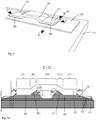
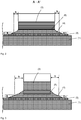
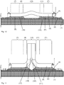
- Fig. 1, Fig. 1a and Fig. 2 each show a detail of a heatable pane 1 according to the invention in the area of the electrical connection element 3.
- the pane 1 is a 3 mm thick, thermally toughened safety glass made of soda-lime glass.
- the disk 1 has a width of 150 cm and a height of 80 cm.
- An electrically conductive structure 2 in the form of a heat conductor structure 2 is printed on the pane 1.
- the electrically conductive structure 2 contains silver particles and glass frits.
- the electrically conductive structure 2 is widened to a width of 10 mm and forms a contact surface for the electrical connection element 3.
- In the edge area of the pane 1 there is also a cover screen print (not shown).
- the solder compound 4 creates a permanent electrical and mechanical connection between the connection element 3 and the electrically conductive structure 2.
- the solder compound 4 contains 57% by weight bismuth, 40% by weight tin and 3% by weight silver.
- the solder mass 4 is arranged completely between the electrical connection element 3 and the electrically conductive structure 2 by a predetermined volume and shape.
- the solder mass 4 has a thickness of 250 ⁇ m.
- the electrical connection element 3 consists of steel with the material number 1.4509 according to EN 10 088-2 (ThyssenKrupp Nirosta® 4509) with a thermal expansion coefficient of 10.0 x 10 -6 / ° C.
- the electrical connection element 3 has a width of 4 mm and a length of 24 mm.
- the transition areas 9 and 11 and the bridge area 10 are flat.
- the bridge region 10 is arranged parallel to the surface of the substrate 1.
- Steel with the material number 1.4509 according to EN 10 088-2 can be easily cold formed and easily welded with all processes except gas welding.
- the steel is used for the construction of silencers and exhaust gas decontamination systems and is particularly suitable for this due to its scaling resistance up to over 950 ° C and corrosion resistance against the stresses occurring in the exhaust system.
- Fig. 3 shows in continuation of the embodiment Figures 1 and 2 an alternative embodiment of the connection element 3 according to the invention.
- the electrical connection element 3 is provided with a silver-containing coating 5 on the surface facing the solder mass 4. This prevents the solder compound from spreading over the coating 5 and limits the exit width b.
- an adhesion-promoting layer for example made of nickel and / or copper, can be located between the connection element 3 and the silver-containing layer 5.
- the exit width b of the solder mass 4 is below 1 mm. Due to the arrangement of the solder mass 4, no critical mechanical stresses are observed in the pane 1.
- the connection of the pane 1 to the electrical connection element 3 is permanently stable via the electrically conductive structure 2.
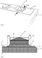
- Fig. 4 shows in continuation of the embodiment Figures 1 and 2 Another alternative embodiment of the connection element 3 according to the invention.
- the electrical connection element 3 contains a recess with a depth of 250 ⁇ m on the surface oriented toward the solder mass 4, which recess forms a solder deposit for the solder mass 4.
- the solder compound 4 can be completely prevented from escaping from the gap.
- the thermal stresses in the pane 1 are not critical and a permanent electrical and mechanical connection is provided between the connection element 3 and the pane 1 via the electrically conductive structure 2.
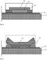
- Fig. 5 shows in continuation of the embodiment Figures 1 and 2 a further alternative embodiment of the connection element 3 according to the invention.
- the electrical connection element 3 is bent up at the edge regions.
- the height of the bend of the edge areas from the glass pane 1 is a maximum of 400 ⁇ m. This creates a space for the solder compound 4.
- the predetermined solder mass 4 forms a concave meniscus between the electrical connection element 3 and the electrically conductive structure 2. An escape of solder 4 from the space can be completely prevented.
- the exit width b is approximately zero, largely below zero due to the meniscus formed.
- the thermal stresses in the pane 1 are not critical and a permanent electrical and mechanical connection is provided between the connection element 3 and the pane 1 via the electrically conductive structure 2.
- FIGS. 6 and 7 each show a detail of a further embodiment of the pane 1 according to the invention with connection element 3.
- the connection element 3 contains an iron-containing alloy with a thermal expansion coefficient of 8 ⁇ 10 -6 / ° C.
- the material thickness is 2 mm.
- hat-shaped compensating bodies 6 with chromium-containing steel of material number 1.4509 according to EN 10 088-2 (ThyssenKrupp Nirosta® 4509) are applied.
- the maximum layer thickness of the hat-shaped compensating body 6 is 4 mm.
- the thermal expansion coefficients of the connection element 3 can be adapted to the requirements of the pane 1 and the solder compound 4 by means of the compensating bodies.
- the hat-shaped compensating bodies 6 lead to an improved heat flow during the production of the solder connection 4.
- the heating occurs primarily in the center of the contact surfaces 8 and 8 '.
- the exit width b of the solder mass 4 can be further reduced. Due to the small exit width b of ⁇ 1 mm and the adapted expansion coefficient, the thermal stresses in the pane 1 can continue be reduced.
- the thermal stresses in the pane 1 are not critical and a permanent electrical and mechanical connection is provided between the connection element 3 and the pane 1 via the electrically conductive structure 2.
- Fig. 8 shows in continuation of the embodiment Figures 1 and 1a an alternative embodiment of the connection element 3 according to the invention.
- the two transition areas 9 and 11 and the bridge area 10 are curved and have the same direction of curvature. Together they form the profile of an arc with a radius of curvature of 12 mm.
- the connections 16 and 16 'between the contact surfaces 8 and 8' and the surfaces 9 'and 11' of the curved transition areas 9 and 11 facing the substrate are shaped as edges.
- the thermal stresses in the pane 1 are not critical and a permanent electrical and mechanical connection is provided between the connection element 3 and the pane 1 via the electrically conductive structure 2.
- Fig. 9 shows in continuation of the embodiment Figures 1 and 1a a further alternative embodiment of the connection element 3 according to the invention.
- the two transition areas are flat, the bridge area is angled.
- the angle ⁇ of the bridge area is 140 °.
- the thermal stresses in the pane 1 are not critical and a permanent electrical and mechanical connection is provided between the connection element 3 and the pane 1 via the electrically conductive structure 2.
- Fig. 10 shows in continuation of the embodiment Figures 1 and 1a a further alternative embodiment of the connection element 3 according to the invention.
- the two transition areas 9 and 11 and the bridge area 10 are curved.
- the structure consisting of the transition areas 9 and 11 and the bridge area 10 changes its direction of curvature twice. Adjacent to the foot regions 7 and 7 ′, the direction of curvature of the transition regions 9 and 11 points away from the substrate 1.
- the underside of the connection element has a continuous course on.
- the thermal stresses in the pane 1 are not critical and a permanent electrical and mechanical connection is provided between the connection element 3 and the pane 1 via the electrically conductive structure 2.
- Fig. 11 shows a further alternative embodiment of the connection element 3 according to the invention.
- the two transition regions 9 and 11 are curved, the direction of curvature pointing away from the substrate 1.
- the bridge area 10 consists of two sub-elements.
- the sub-elements each have a curved sub-area 17 and 17 'and a planar sub-area 18 and 18'.
- the bridge area 10 is connected to the transition area 9 by the sub-area 17 and to the transition area 11 by the sub-area 17 '.
- the curved partial areas 17 and 17 ' have the same direction of curvature as the adjoining transition area.
- the planar partial areas 18 and 18 ' are arranged perpendicular to the surface of the substrate and are in direct contact with one another.
- Fig. 12 shows in continuation of the embodiment Figures 1 and 1a Another alternative embodiment of the connection element 3 according to the invention.
- the foot regions 7 and 7 ', the transition regions 9 and 11 and the bridge region 10 are according to FIG Figure 1a shaped.
- the contact surfaces 8 and 8 ' have a width of 4 mm and a length of 4 mm.
- Spacers 19 are attached to the contact surfaces 8 and 8 '.
- the spacers are shaped as hemispheres and have a height h of 2.5 x 10 -4 m and a width I of 5 x 10 -4 m.
- the spacers 19 can also be configured, for example, as a cube, a pyramid or a segment of an ellipsoid of revolution and preferably have a width of 0.5 ⁇ 10 -4 m to 10 ⁇ 10 -4 m and a height of 0.5 ⁇ 10 -4 m to 5 ⁇ 10 -4 m, particularly preferably from 1x 10 -4 m to 3 ⁇ 10 -4 m.
- the spacers 19 promote the formation of a uniform layer of the solder mass 4. This is particularly advantageous with regard to the adhesion of the connection element 3.
- Figure 12a shows in continuation of the embodiment Figure 12 a further alternative embodiment of the connection element 3 according to the invention.
- a contact bump 22 is arranged on each surface of the foot regions 7, 7 ′ applied by the substrate 1.
- the contact elevations 22 are shaped as hemispheres and have a height of 2.5 x 10 -4 m and a width of 5 x 10 -4 m.
- the center points of the contact elevations 22 are arranged approximately in the geometric center of the surfaces of the foot regions 7, 7 ′ applied by the substrate 1. Due to their convex surface, the contact elevations 22 enable an advantageously improved soldering of the connection element 3 to the electrically conductive structure 2. For soldering, electrodes can be used whose contact side is flat.
- the electrode area is brought into contact with the contact bump 22, the contact area between the electrode area and contact bump 22 forming the soldering point.
- the position of the soldering point is preferably determined by the point on the convex surface of the contact elevation 22 which has the greatest perpendicular distance to the surface of the substrate 1.
- the position of the soldering point is independent of the position of the soldering electrode on the connection element 3. This is particularly advantageous with regard to a reproducible, uniform heat distribution during the soldering process.
- the heat distribution during the soldering process is determined by the position, size, arrangement and geometry of the contact bump 22.
- the contact elevation 22 can be shaped, for example, as a segment of an ellipsoid of revolution or as a cuboid, the surface of the cuboid facing away from the substrate being convexly curved.
- the contact elevations 22 preferably have a height of 0.1 mm to 2 mm, particularly preferably 0.2 mm to 1 mm.
- the length and width of the contact bumps 22 is preferably between 0.1 and 5 mm, very particularly preferably between 0.4 mm and 3 mm.
- the contact bumps 22 and the spacers 19 can be formed in one piece with the connection element 3 in an advantageous embodiment.
- the contact bumps 22 and the spacers 19 can be formed on the surface, for example, by reshaping a connection element 3 with a surface that is planar in the initial state, for example by embossing or deep drawing. In this case, a corresponding depression can be produced on the surface of the connection element 3 opposite the contact elevation 22 or the spacer 19.
- a homogeneous, uniformly thick and uniformly melted layer of the solder mass 4 is achieved by the contact bumps 22 and the spacers 19.
- mechanical stresses between connection element 3 and substrate 1 be reduced. This is particularly advantageous when using lead-free solder masses, which are less able to compensate for mechanical stresses due to their lower ductility compared to lead-containing solder masses.
- Fig. 13 shows a plan view of an alternative embodiment of the connection element 3 according to the invention.
- the transition areas 9 and 11 and the bridge area 10 are according to FIG Figure 1a shaped.
- Each foot area 7 and 7 ' has a width of 8 mm and is twice as wide as the transition areas 9 and 11 and the bridge area 10. It has surprisingly been shown that foot areas 7, 7' which are wider than the transition areas 9, 11 and the bridge area 10 lead to a reduction in the mechanical stresses in the pane 1.
- the width of the foot regions 7, 7 ′ is preferably from 150% to 300% of the width of the bridge region 10.
- Fig. 14 shows a perspective view of an alternative embodiment of the connection element 3 according to the invention.
- the foot regions 7 and 7 ' have, for example, a length of 7 mm and a width of 5 mm.
- the bridge area 10 is designed flat and has a length of 12 mm and a width of 10 mm, for example.
- the bridge area 10 is wider than the foot areas 7, 7 'and has a production-related recess 21.
- the recess 21 extends up to the edge of the bridge area 10, to which the foot area 7 adjoins via the transition area 9.
- the shape and size of the recess 21 correspond to the section of the connection element 3 from the foot region 7 and the transition region 9.
- the contact surfaces 8 and 8 'on the undersides of the foot regions 7 and 7' have a rectangular shape, the two each from the bridge region 10 facing away corners are chamfered.
- the chamfering prevents angles that are too small, in particular 90 ° angles along the circumferential side edges of the contact surfaces 8, 8 '. It has been shown that this can reduce mechanical stresses in the disk.
- connection element 3 contains a connection plug 20 arranged on the bridge area 10.
- the connection plug 20 is connected to the bridge area 10 on the side edge of the bridge area 10 adjoining the transition area 9.
- the connection plug 20 is designed as a standard-compliant flat plug connector onto which the coupling of a connecting cable (not shown), for example to the on-board electrical system, can be plugged.
- connection element 3 lies in the simple production of the connection element 3 while at the same time providing a convenient interface for electrical contacting (connection plug 20).
- the foot areas 7, 7 ', the transition areas 9, 11, the bridge area 10 and the connector 20 are formed in one piece.
- the connection element 3 is provided in a planar initial state in which the sections provided as the transition area 9 and as the foot area 7 are arranged within the recess 21. In the initial state, the transition region 11 and the foot region 7 ′ are arranged in the same plane as the bridge region 10. In the initial state, the connector 20 is also arranged in the same plane as the bridge region 10.
- the area provided as the foot area 7 and transition area 9 can be separated from the bridge area 10, for example by punching, laser processing or water jet processing, with a connection via the connecting edge between the transition area 9 and the bridge area 10 remaining.
- the connecting plug 20 is bent around the connecting line between the connecting plug 20 and the bridge area 10 into the position shown, the surface facing upward in the initial state facing the bridge area 10.
- the transition area 9 and the foot area 7 are bent into the position shown using the connecting line between the transition area 9 and the bridge area 10, the surface facing upwards in the initial state then forming the undersides of the foot area 7 and the transition area 9.
- the recess 21 is formed by bending the transition area 9 and the foot area 7.
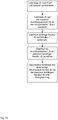
- Fig. 15 shows in detail a method according to the invention for producing a pane 1 with an electrical connection element 3.
- an example of the method according to the invention for producing a pane with an electrical connection element 3 is shown.
- As a first step it is necessary to portion the solder mass 4 according to shape and volume.
- the portioned solder mass 4 is arranged on the contact surfaces 8 and 8 ′ of the electrical connection element 3.
- the electrical connection element 3 is arranged with the solder compound 4 on the electrically conductive structure 2.
- Test samples were made with the pane 1 (thickness 3 mm, width 150 cm and height 80 cm), the electrically conductive structure 2 in the form of a heat conductor structure, the electrical connection element 3 according to Figure 1 , the silver layer 5 on the contact surfaces 8 and 8 'of the connection element 3 and the solder mass 4.
- the material thickness of the connection element 3 was 0.8 mm.
- the connection element 3 contained steel with the material number 1.4509 according to EN 10 088-2 (ThyssenKrupp Nirosta® 4509).
- the contact surfaces 8 and 8 'of the connection element 3 had a width of 4 mm and a length of 4 mm.
- the solder compound 4 was previously applied to the contact surfaces 8 and 8 ′ of the connection element 3 as a plate with a defined layer thickness, volume and shape.
- the connection element 3 was attached to the electrically conductive structure 2 with the solder compound 4 attached.
- connection element 3 The dimensions and compositions of the electrical connection element 3, the silver layer 5 on the contact surfaces 8 and 8 ′ of the connection element 3 and the solder mass 4 are shown in Table 1. Due to the arrangement of the solder mass 4, predetermined by the connection element 3 and the electrically conductive structure 2, no critical mechanical stresses were observed in the pane 1. The connection of the pane 1 to the electrical connection element 3 was permanently stable via the electrically conductive structure 2.
- connection element 3 contained an iron-nickel-cobalt alloy.
- the dimensions and compositions of the electrical connection element 3, the silver layer 5 on the contact surfaces 8 and 8 ′ of the connection element 3 and the solder mass 4 are shown in Table 2.
- connection element 3 contained an iron-nickel alloy.
- the dimensions and compositions of the electrical connection element 3, the silver layer 5 on the contact surfaces 8 and 8 ′ of the connection element 3 and the solder mass 4 are shown in Table 3.
- connection element 3 Steel of material number 1.4509 according to EN 10 088-2 with the composition: Iron (wt%) 78.87 Carbon (wt%) 0.03 Chromium (wt%) 18.5 Titanium (wt .-%) 0.6 Niobium (wt%) 1 Manganese (wt%) 1 CTE (coefficient of thermal expansion) (10 -6 / ° C for 0 ° C - 100 ° C) 10 Difference between CTE connection element and substrate (10 -6 / ° C for 0 ° C - 100 ° C) 1.7 Thickness of connection element (m) 8.0 x 10 -4 Angle ⁇ (°) 40 Wetting layer 5 Silver (wt .-%) 100 Thickness of layer (m) 7.0 x 10 -6 Solder mass 4 Tin (wt%) 40 Bismuth (wt%) 57 Silver (wt .-%) 3
- connection element 3 contained steel with the material number 1.4509 according to EN 10 088-2 (ThyssenKrupp Nirosta® 4509). The difference was in the shape of the connector. According to the prior art, the angle ⁇ was 90 °. In this way, no capillary forces could develop at the edges of the contact surfaces 8 and 8 '.
- the dimensions and components of the electrical connection element 3, the metal layer on the contact surfaces 8 and 8 ′ of the connection element 3 and the solder mass 4 are shown in Table 4.
- connection element 3 was soldered to the electrically conductive structure 2 using conventional methods using the solder compound 4.
- the large exit width led to critical mechanical stresses in the disc.
- connection element 3 was soldered to the electrically conductive structure 2 using conventional methods using the solder compound 4.
- the large difference in the thermal expansion coefficients between connection element 3 and substrate 1 as well as the large exit width led to critical mechanical stresses in the pane.
- Table 7 Execution according to the invention, example Table 1 Table 2 Table 3 material Steel of material number 1.4509 according to EN 10 088-2 Iron (54 wt%) nickel (29 wt%) cobalt (17 wt%) Iron (65% by weight) nickel (35% by weight) CTE (coefficient of thermal expansion) of the connection element (10 -6 / ° C for 0 ° C - 100 ° C) 10 5.1 1.7 Difference between the CTE of the connection element and the substrate (10 -6 / ° C for 0 ° C - 100 ° C) 1.7 3.2 6.6 Angle ⁇ (°) 40 40 40 40 40 Exit width b (mm) 0.4 0.4 0.4 observation stable against sudden drops in temperature stable against sudden drops in temperature stable against sudden drops in temperature Comparative example 1 Comparative example 2 Comparative example 3 Table 4 Table 5 Table 6 material Steel of material number 1.4509 according to EN 10 088-2 Titanium (10
- panes according to the invention with glass substrates 1 and electrical connection elements 3 according to the invention have a smaller exit width and better stability against sudden temperature differences.
Landscapes
- Engineering & Computer Science (AREA)
- Mechanical Engineering (AREA)
- Manufacturing & Machinery (AREA)
- Physics & Mathematics (AREA)
- Optics & Photonics (AREA)
- Connections Effected By Soldering, Adhesion, Or Permanent Deformation (AREA)
- Coupling Device And Connection With Printed Circuit (AREA)
- Manufacturing Of Electrical Connectors (AREA)
- Resistance Heating (AREA)
- Combinations Of Printed Boards (AREA)
- Surface Treatment Of Glass (AREA)
- Surface Heating Bodies (AREA)
- Joining Of Glass To Other Materials (AREA)
- Multi-Conductor Connections (AREA)
Priority Applications (1)
| Application Number | Priority Date | Filing Date | Title |
|---|---|---|---|
| PL20184104T PL3751960T3 (pl) | 2011-05-10 | 2012-04-17 | Szyba z elektrycznym elementem przyłączeniowym |
Applications Claiming Priority (5)
| Application Number | Priority Date | Filing Date | Title |
|---|---|---|---|
| EP11165504 | 2011-05-10 | ||
| EP11165506 | 2011-05-10 | ||
| PCT/EP2012/056965 WO2012152544A1 (fr) | 2011-05-10 | 2012-04-17 | Vitre pourvue d'un élément de connexion électrique |
| EP19152140.0A EP3500063B1 (fr) | 2011-05-10 | 2012-04-17 | Vitre dotée d'un élément de raccordement électrique |
| EP12717090.0A EP2708093B1 (fr) | 2011-05-10 | 2012-04-17 | Vitre pourvue d'un élément de connexion électrique |
Related Parent Applications (3)
| Application Number | Title | Priority Date | Filing Date |
|---|---|---|---|
| EP12717090.0A Division EP2708093B1 (fr) | 2011-05-10 | 2012-04-17 | Vitre pourvue d'un élément de connexion électrique |
| EP19152140.0A Division EP3500063B1 (fr) | 2011-05-10 | 2012-04-17 | Vitre dotée d'un élément de raccordement électrique |
| EP19152140.0A Division-Into EP3500063B1 (fr) | 2011-05-10 | 2012-04-17 | Vitre dotée d'un élément de raccordement électrique |
Publications (2)
| Publication Number | Publication Date |
|---|---|
| EP3751960A1 true EP3751960A1 (fr) | 2020-12-16 |
| EP3751960B1 EP3751960B1 (fr) | 2022-04-27 |
Family
ID=46001199
Family Applications (3)
| Application Number | Title | Priority Date | Filing Date |
|---|---|---|---|
| EP19152140.0A Active EP3500063B1 (fr) | 2011-05-10 | 2012-04-17 | Vitre dotée d'un élément de raccordement électrique |
| EP20184104.6A Active EP3751960B1 (fr) | 2011-05-10 | 2012-04-17 | Vitre dotée d'un élément de raccordement électrique |
| EP12717090.0A Active EP2708093B1 (fr) | 2011-05-10 | 2012-04-17 | Vitre pourvue d'un élément de connexion électrique |
Family Applications Before (1)
| Application Number | Title | Priority Date | Filing Date |
|---|---|---|---|
| EP19152140.0A Active EP3500063B1 (fr) | 2011-05-10 | 2012-04-17 | Vitre dotée d'un élément de raccordement électrique |
Family Applications After (1)
| Application Number | Title | Priority Date | Filing Date |
|---|---|---|---|
| EP12717090.0A Active EP2708093B1 (fr) | 2011-05-10 | 2012-04-17 | Vitre pourvue d'un élément de connexion électrique |
Country Status (16)
| Country | Link |
|---|---|
| US (1) | US10305239B2 (fr) |
| EP (3) | EP3500063B1 (fr) |
| JP (4) | JP2014519150A (fr) |
| KR (1) | KR101567184B1 (fr) |
| CN (1) | CN103262645B (fr) |
| AR (1) | AR086302A1 (fr) |
| DE (2) | DE202012012674U1 (fr) |
| DK (1) | DK2708093T3 (fr) |
| EA (1) | EA028379B1 (fr) |
| ES (3) | ES2918473T3 (fr) |
| HU (2) | HUE047512T2 (fr) |
| MX (1) | MX2013013015A (fr) |
| PL (3) | PL3751960T3 (fr) |
| PT (2) | PT2708093T (fr) |
| TW (1) | TWI464131B (fr) |
| WO (1) | WO2012152544A1 (fr) |
Families Citing this family (24)
| Publication number | Priority date | Publication date | Assignee | Title |
|---|---|---|---|---|
| BR112013028049B1 (pt) | 2011-05-10 | 2020-10-06 | Saint-Gobain Glass France | Painel com pelo menos um elemento de conexão elétrico,método para produção e uso de tal painel |
| KR101553762B1 (ko) | 2011-05-10 | 2015-09-16 | 쌩-고벵 글래스 프랑스 | 전기 연결 요소를 구비한 창유리 |
| PT2896269T (pt) | 2012-09-14 | 2017-06-23 | Saint Gobain | Placa de vidro com um elemento de ligação elétrica |
| MY170325A (en) | 2012-09-14 | 2019-07-17 | Saint Gobain | Pane with an electrical connection element |
| AR097558A1 (es) * | 2013-10-29 | 2016-03-23 | Saint Gobain | Entrepaño con -al menos- dos elementos de conexión eléctrica y un conductor de conexión |
| DE102013226933A1 (de) * | 2013-12-20 | 2015-06-25 | Continental Automotive Gmbh | Elektrisches Kontaktelement, Schaltungsanordnung und Verfahren zum Herstellen einer Schaltungsanordnung |
| DE102014206739A1 (de) * | 2014-04-08 | 2015-10-08 | Bayerische Motoren Werke Aktiengesellschaft | Schubfeld für einen Vorderwagen einer Fahrzeugkarosserie eines Fahrzeugs und Fahrzeug |
| DE202015002764U1 (de) * | 2014-09-12 | 2015-05-06 | Few Fahrzeugelektrikwerk Gmbh & Co. Kg | Kontaktelement zum Löten mittels elektromagnetischer Induktionserwärmung |
| CA2984056C (fr) * | 2015-05-05 | 2020-03-24 | Saint-Gobain Glass France | Disque comprenant un element de branchement electrique et un element de liaison installe sur ce dernier |
| JP6725971B2 (ja) * | 2015-07-14 | 2020-07-22 | 日本板硝子株式会社 | ガラス板モジュール |
| GB201514397D0 (en) * | 2015-08-13 | 2015-09-30 | Pilkington Group Ltd | Electrical Connector |
| DE102016125897B4 (de) * | 2016-02-11 | 2022-06-23 | Few Fahrzeugelektrikwerk Gmbh & Co. Kg | Lötfähiges elektrisches Anschlusselement |
| USD857420S1 (en) * | 2016-12-23 | 2019-08-27 | Few Fahrzeugelektrikwerk Gmbh & Co. Kg | Mounting device |
| DE202016008092U1 (de) * | 2016-12-28 | 2017-03-03 | Few Fahrzeugelektrikwerk Gmbh & Co. Kg | Elektrisches Anschlusselement |
| US11490465B2 (en) | 2017-03-02 | 2022-11-01 | Pilkington Group Limited | Window assembly having a terminal connector |
| KR102480461B1 (ko) * | 2017-11-30 | 2022-12-21 | 쌩-고벵 글래스 프랑스 | 차량용 창유리의 터미널 솔더링 장치 및 방법 |
| JP7100980B2 (ja) | 2018-01-22 | 2022-07-14 | ローム株式会社 | Ledパッケージ |
| GB201804622D0 (en) * | 2018-03-22 | 2018-05-09 | Central Glass Co Ltd | Method of producing a vehicle glass assembly |
| WO2020001977A1 (fr) | 2018-06-26 | 2020-01-02 | Saint-Gobain Glass France | Disque comprenant un élément de raccordement électrique et un câble de raccordement |
| USD924810S1 (en) * | 2019-01-04 | 2021-07-13 | Intel Corporation | Busbar |
| DE102020114650B3 (de) * | 2020-06-02 | 2021-06-02 | Semikron Elektronik Gmbh & Co. Kg | Leistungselektronische Baugruppe mit einer elektrisch leitenden Hülse und mit einem Schaltungsträger |
| DE102021120217B3 (de) * | 2021-08-04 | 2022-09-29 | Lisa Dräxlmaier GmbH | Vorrichtung und Verfahren zur Kontaktierung eines Leiters |
| US12562541B2 (en) * | 2023-04-28 | 2026-02-24 | Logitech Europe S.A. | Techniques for soldering on a substrate with a below soldering temperature melting point |
| SE548155C2 (en) * | 2023-05-09 | 2026-04-13 | Safetrack Infrasystems Sisab Ab | Improved cable connecting piece |
Citations (6)
| Publication number | Priority date | Publication date | Assignee | Title |
|---|---|---|---|---|
| JPH0658557U (ja) * | 1993-01-14 | 1994-08-12 | 旭硝子株式会社 | 導電端子 |
| WO2004068643A1 (fr) * | 2003-01-30 | 2004-08-12 | Pilkington Plc | Panneau de vitrage pour automobile |
| EP1488972A1 (fr) * | 2002-03-11 | 2004-12-22 | Nippon Sheet Glass Co., Ltd. | Article de verre assemble au moyen d'une fixation metallique, et structure de joint utilisant ledit article |
| WO2007110610A1 (fr) * | 2006-03-24 | 2007-10-04 | Pilkington Group Limited | connecteur électrique |
| EP1942703A2 (fr) | 2007-01-02 | 2008-07-09 | Agc Automotive Americas R&D, Inc. | Connecteur électrique pour vitre de fenêtre de véhicule |
| DE202008015441U1 (de) * | 2008-11-20 | 2010-04-08 | Few Fahrzeugelektrikwerk Gmbh & Co. Kg | Lötanschluss |
Family Cites Families (101)
| Publication number | Priority date | Publication date | Assignee | Title |
|---|---|---|---|---|
| US2062335A (en) | 1929-07-05 | 1936-12-01 | Westinghouse Electric & Mfg Co | Glass metal seal |
| US2481385A (en) * | 1944-03-31 | 1949-09-06 | Armco Steel Corp | Weld and weld rod |
| US2672414A (en) | 1950-01-27 | 1954-03-16 | United States Steel Corp | Chromium-titanium steel adapted for sealing to glass |
| US2644066A (en) * | 1951-07-05 | 1953-06-30 | Blue Ridge Glass Corp | Electrical connector for resistance elements on glass plates |
| US2709211A (en) | 1953-05-27 | 1955-05-24 | Blue Ridge Glass Corp | Electrical connectors for resistance elements on glass plates |
| FR1104595A (fr) | 1953-05-27 | 1955-11-22 | Saint Gobain | Raccords électriques pour éléments de résistance sur des plaques de verre |
| US2736649A (en) | 1953-12-04 | 1956-02-28 | United States Steel Corp | Ferritic stainless steel |
| US3088833A (en) | 1960-06-06 | 1963-05-07 | Owens Illinois Glass Co | Sealing glass |
| US3204326A (en) | 1960-12-19 | 1965-09-07 | American Optical Corp | Multi-element energy-conducting structures and method of making the same |
| FR1527738A (fr) * | 1966-09-13 | 1968-06-07 | Saint Gobain | Raccord électrique pour vitrages chauffants, notamment de véhicules |
| DE1936780A1 (de) | 1968-07-23 | 1970-02-26 | Ppg Industries Inc | Heizvorrichtung in Kombination mit einer Antennenvorrichtung |
| US3484584A (en) | 1968-07-23 | 1969-12-16 | Ppg Industries Inc | Combination of electrically heated transparent window and antenna |
| US3534148A (en) | 1969-02-11 | 1970-10-13 | Sybron Corp | Encapsulated electrical circuit and terminals and method of making the same |
| US3746536A (en) | 1970-08-07 | 1973-07-17 | Tokyo Shibaura Electric Co | Sealing alloy |
| US3746586A (en) * | 1971-03-29 | 1973-07-17 | Gen Electric | Precipitation hardenable ferritic iron-chromium-titaniium alloys |
| US4023008A (en) * | 1972-12-28 | 1977-05-10 | Saint-Gobain Industries | Terminal connection for electric heaters for vehicle windows |
| US3880369A (en) * | 1973-09-21 | 1975-04-29 | Boehler & Co Ag Geb | Impact strip for impact pulverizers |
| FR2430847A1 (fr) | 1978-07-13 | 1980-02-08 | Saint Gobain | Vitrage chauffant et/ou d'alarme |
| US4179285A (en) | 1978-07-27 | 1979-12-18 | Armco Inc. | Ferritic stainless steel |
| US4246467A (en) | 1979-07-20 | 1981-01-20 | Ford Motor Company | Electric terminal for connecting a heating grid on a thermal window |
| JPS5929155B2 (ja) | 1979-11-12 | 1984-07-18 | 富士通株式会社 | 半導体記憶装置 |
| JPS5734972U (fr) * | 1980-08-06 | 1982-02-24 | ||
| US4498096A (en) | 1981-01-30 | 1985-02-05 | Motorola, Inc. | Button rectifier package for non-planar die |
| JPS57197761A (en) * | 1981-05-29 | 1982-12-04 | Nippon Sheet Glass Co Ltd | Terminal bonding structure |
| JPS5853372U (ja) * | 1981-09-29 | 1983-04-11 | 日本板硝子株式会社 | 端子の接合構造 |
| JPS60208076A (ja) * | 1984-04-02 | 1985-10-19 | 松下電器産業株式会社 | シ−ズヒ−タ |
| JPS60212987A (ja) * | 1984-04-09 | 1985-10-25 | 松下電器産業株式会社 | シ−ズヒ−タ |
| KR930003957B1 (ko) * | 1987-05-09 | 1993-05-17 | 후다바 덴시 고오교오 가부시끼가이샤 | 형광표시관 |
| DE9013380U1 (de) | 1990-09-21 | 1990-11-29 | SEKURIT SAINT-GOBAIN Deutschland GmbH & Co. KG, 52066 Aachen | Stromanschlußelement für eine heizbare Autoglasscheibe |
| FR2670070B1 (fr) * | 1990-11-30 | 1996-09-20 | Saint Gobain Vitrage Int | Pieces de connexion pour vitrages electrifies. |
| IT1245182B (it) * | 1991-03-08 | 1994-09-13 | Ezio Curti | Procedimento e dispositivo, per fissare un connettore elettrico ad una superficie conduttiva |
| JP2908922B2 (ja) * | 1991-11-29 | 1999-06-23 | 株式会社日立製作所 | 半導体装置およびその製造方法 |
| JPH0696847A (ja) | 1992-09-11 | 1994-04-08 | Matsushita Electric Ind Co Ltd | 面状発熱体およびその製造法 |
| DE4439645C1 (de) * | 1994-11-07 | 1996-04-11 | Sekurit Saint Gobain Deutsch | Stromanschlußelement für eine heizbare Autoglasscheibe |
| US5596335A (en) | 1994-12-27 | 1997-01-21 | Ppg Industries, Inc. | Electrical connector |
| JP3439866B2 (ja) | 1995-03-08 | 2003-08-25 | 日本冶金工業株式会社 | 耐食性および溶接性に優れるフェライト系ステンレス鋼 |
| JPH09139565A (ja) | 1995-11-15 | 1997-05-27 | Dainippon Printing Co Ltd | 電極パターン形成方法 |
| JPH09226522A (ja) | 1996-02-29 | 1997-09-02 | Central Glass Co Ltd | 導電端子 |
| JP3390617B2 (ja) | 1996-11-29 | 2003-03-24 | 京セラ株式会社 | 半導体素子収納用パッケージ |
| US5961737A (en) | 1996-12-12 | 1999-10-05 | Hughes Electronics Corporation | Welded wire termination device and method for constructing a solar array |
| GB9707368D0 (en) | 1997-04-11 | 1997-05-28 | Splifar S A | Electrical connection stud |
| JP3498893B2 (ja) | 1998-04-23 | 2004-02-23 | セントラル硝子株式会社 | 導電体ペースト |
| JPH11347785A (ja) * | 1998-06-04 | 1999-12-21 | Hitachi Ltd | 半導体ダイボンディング用半田とそのテープ及び半導体装置 |
| US6475043B2 (en) | 1998-11-25 | 2002-11-05 | Antaya Technologies Corporation | Circular electrical connector |
| JP4334054B2 (ja) | 1999-03-26 | 2009-09-16 | 株式会社東芝 | セラミックス回路基板 |
| JP2001126648A (ja) * | 1999-10-22 | 2001-05-11 | Futaba Corp | 蛍光表示装置 |
| MXPA02007040A (es) | 2000-01-25 | 2003-09-25 | Siv Soc Italiana Vetro | Vidrio con terminal electrica. |
| US6638120B2 (en) | 2000-02-21 | 2003-10-28 | Larry J. Costa | Snap electrical terminal |
| DE10018276A1 (de) | 2000-04-13 | 2001-10-25 | Saint Gobain Sekurit D Gmbh | Verbundscheibe |
| ATE347742T1 (de) | 2000-06-02 | 2006-12-15 | Saint Gobain | Elektrisches lötbares verbindungselement mit lötstelle |
| DE10046489C1 (de) | 2000-06-02 | 2001-12-20 | Saint Gobain Sekurit D Gmbh | Lötbares elektrisches Anschlußelement mit Lotdepot und dessen Verwendung |
| TWI248842B (en) | 2000-06-12 | 2006-02-11 | Hitachi Ltd | Semiconductor device and semiconductor module |
| US6406337B1 (en) | 2000-09-27 | 2002-06-18 | Antaya Technologies Corporation | Glass mounted electrical terminal |
| US6816385B1 (en) | 2000-11-16 | 2004-11-09 | International Business Machines Corporation | Compliant laminate connector |
| JP2002167245A (ja) * | 2000-11-30 | 2002-06-11 | Nippon Sheet Glass Co Ltd | ガラスパネル製造方法 |
| JP2003050341A (ja) * | 2001-08-06 | 2003-02-21 | Yamaha Corp | 光学部品複合体およびその製造方法 |
| US20050029666A1 (en) | 2001-08-31 | 2005-02-10 | Yasutoshi Kurihara | Semiconductor device structural body and electronic device |
| JP2003124416A (ja) | 2001-10-16 | 2003-04-25 | Yazaki Corp | チップ部品のバスバーへの接合構造 |
| DE20203202U1 (de) | 2001-12-31 | 2002-06-06 | Gilliam, Jakob, Dipl.-Ing., 82402 Seeshaupt | Elektrischer Anschluß |
| US6685514B2 (en) | 2002-04-05 | 2004-02-03 | Larry J. Costa | Folding blade electrical terminal |
| US6840780B1 (en) | 2002-07-26 | 2005-01-11 | Antaya Technologies Corporation | Non-solder adhesive terminal |
| US6790104B2 (en) | 2002-07-26 | 2004-09-14 | Antaya Technologies Corporation | Electrical terminal |
| US7675004B2 (en) | 2004-03-12 | 2010-03-09 | Panasonic Corporation | Heating element and production method thereof |
| DE102004050158B3 (de) | 2004-10-15 | 2006-04-06 | Saint-Gobain Sekurit Deutschland Gmbh & Co. Kg | Transparente Scheibe mit einer beheizbaren Beschichtung |
| US20070224842A1 (en) | 2004-11-12 | 2007-09-27 | Agc Automotive Americas R&D, Inc. | Electrical Connector For A Window Pane Of A Vehicle |
| US7134201B2 (en) | 2004-11-12 | 2006-11-14 | Agc Automotive Americas R&D, Inc. | Window pane and a method of bonding a connector to the window pane |
| DE102004057630B3 (de) * | 2004-11-30 | 2006-03-30 | Saint-Gobain Sekurit Deutschland Gmbh & Co. Kg | Verfahren und Vorrichtung zum Löten von Anschlüssen mit Induktionswärme |
| JPWO2006098160A1 (ja) | 2005-03-14 | 2008-08-21 | 株式会社村田製作所 | 導電性ペーストおよびガラス構造体 |
| WO2006132319A1 (fr) | 2005-06-08 | 2006-12-14 | Nippon Sheet Glass Co., Ltd. | Objet en verre comportant un film conducteur formé sur celui-ci et procédé pour le fabriquer |
| US20070030064A1 (en) | 2005-08-03 | 2007-02-08 | Yinglei Yu | Integrated laterally diffused metal oxide semiconductor power detector |
| JP4550791B2 (ja) | 2005-11-24 | 2010-09-22 | 古河電気工業株式会社 | アルミ撚線用圧着端子および前記圧着端子が接続されたアルミ撚線の端末構造 |
| JP4934325B2 (ja) | 2006-02-17 | 2012-05-16 | 株式会社フジクラ | プリント配線板の接続構造及びプリント配線板の接続方法 |
| GB0605883D0 (en) | 2006-03-24 | 2006-05-03 | Pilkington Plc | Electrical connector |
| DE102006017675A1 (de) | 2006-04-12 | 2007-10-18 | Pilkington Automotive Deutschland Gmbh | Glasscheibe mit elektrischem Funktionselement mit durch Lötverbindung befestigten Anschlußdrähten und Verfahren zum Herstellen elektrischer Anschlüsse |
| JPWO2007125939A1 (ja) * | 2006-04-27 | 2009-09-10 | 株式会社Neomaxマテリアル | 配線接続用クラッド材及びそのクラッド材から加工された配線接続部材 |
| JP2007335260A (ja) | 2006-06-15 | 2007-12-27 | Epson Imaging Devices Corp | 基板の接続端子と被覆導体線との接続構造 |
| JP2008041518A (ja) | 2006-08-09 | 2008-02-21 | Noritake Itron Corp | 蛍光表示管の製造方法および蛍光表示管 |
| JP4907734B2 (ja) | 2007-05-07 | 2012-04-04 | エクスアテック、エル.エル.シー. | 導電性グリッドを有するプラスチックパネルの電気接続 |
| JP2009057630A (ja) * | 2007-08-07 | 2009-03-19 | Mitsubishi Shindoh Co Ltd | Snメッキ導電材料及びその製造方法並びに通電部品 |
| JP4856025B2 (ja) * | 2007-08-10 | 2012-01-18 | セイコーインスツル株式会社 | 気密端子の製造方法及び気密端子、圧電振動子の製造方法及び圧電振動子、発振器、電子機器、電波時計 |
| JP2009064579A (ja) | 2007-09-04 | 2009-03-26 | Nippon Sheet Glass Co Ltd | 導電機能付板状体の端子構造体及び導電機能付板状体 |
| FR2921520B1 (fr) * | 2007-09-20 | 2014-03-14 | Saint Gobain | Element de connexion electrique et vitrage pourvu d'un tel element |
| CN101933139B (zh) | 2007-12-20 | 2012-11-07 | 爱信艾达株式会社 | 半导体装置及其制造方法 |
| JP5546531B2 (ja) | 2008-05-08 | 2014-07-09 | オウトクンプ ファオデーエム ゲゼルシャフト ミット ベシュレンクテル ハフツング | 鉄ニッケル合金 |
| JP2010020918A (ja) | 2008-07-08 | 2010-01-28 | Nippon Sheet Glass Co Ltd | 端子構造及び車両用端子付ガラス板 |
| JP5156580B2 (ja) | 2008-10-31 | 2013-03-06 | 株式会社オートネットワーク技術研究所 | コネクタ |
| DE102009016353B4 (de) * | 2009-04-07 | 2022-06-30 | Few Fahrzeugelektrik Werk Gmbh & Co. Kg | Anschlusskontakt für an Scheiben von Fahrzeugen vorgesehene elektrische Einrichtungen |
| TWI404972B (zh) | 2009-06-19 | 2013-08-11 | Largan Precision Co | 成像光學鏡組 |
| EP2365730A1 (fr) | 2010-03-02 | 2011-09-14 | Saint-Gobain Glass France | Disque doté d'un élément de raccordement électrique |
| DE102010018860B4 (de) | 2010-04-30 | 2014-10-09 | Few Fahrzeugelektrikwerk Gmbh & Co. Kg | Kontaktierungsanordnung für auf flächigen Gebilden, insbesondere Glasscheiben, vorhandene Leiter |
| EP2408260A1 (fr) | 2010-07-13 | 2012-01-18 | Saint-Gobain Glass France | palque de verre dotée d'un élément de raccordement électrique |
| US20120060559A1 (en) | 2010-09-14 | 2012-03-15 | E. I. Du Pont De Nemours And Company | Process for coating glass onto a flexible stainless steel substrate |
| DE202011100906U1 (de) | 2011-05-03 | 2011-06-09 | FEW Fahrzeugelektrikwerk GmbH & Co. KG, 04442 | Elektrisches Anschlusselement |
| KR101553762B1 (ko) | 2011-05-10 | 2015-09-16 | 쌩-고벵 글래스 프랑스 | 전기 연결 요소를 구비한 창유리 |
| BR112013028049B1 (pt) | 2011-05-10 | 2020-10-06 | Saint-Gobain Glass France | Painel com pelo menos um elemento de conexão elétrico,método para produção e uso de tal painel |
| JP6021906B2 (ja) | 2011-07-04 | 2016-11-09 | サン−ゴバン グラス フランスSaint−Gobain Glass France | 電気接続部材を有するウィンドウガラスの製造方法 |
| WO2013073068A1 (fr) | 2011-11-16 | 2013-05-23 | エム・テクニック株式会社 | Procédé pour produire des particules d'alliage argent-cuivre |
| PT2896269T (pt) | 2012-09-14 | 2017-06-23 | Saint Gobain | Placa de vidro com um elemento de ligação elétrica |
| JP2015119072A (ja) | 2013-12-19 | 2015-06-25 | 富士電機株式会社 | レーザ溶接方法、レーザ溶接治具、半導体装置 |
| USD815042S1 (en) | 2015-03-26 | 2018-04-10 | Few Fahrzeugelektrikwerk Gmbh & Co. Kg | Mounting device |
| JP6725971B2 (ja) * | 2015-07-14 | 2020-07-22 | 日本板硝子株式会社 | ガラス板モジュール |
-
2012
- 2012-04-17 MX MX2013013015A patent/MX2013013015A/es active IP Right Grant
- 2012-04-17 EA EA201391657A patent/EA028379B1/ru not_active IP Right Cessation
- 2012-04-17 JP JP2014509652A patent/JP2014519150A/ja active Pending
- 2012-04-17 ES ES20184104T patent/ES2918473T3/es active Active
- 2012-04-17 HU HUE12717090A patent/HUE047512T2/hu unknown
- 2012-04-17 PL PL20184104T patent/PL3751960T3/pl unknown
- 2012-04-17 WO PCT/EP2012/056965 patent/WO2012152544A1/fr not_active Ceased
- 2012-04-17 PL PL19152140.0T patent/PL3500063T3/pl unknown
- 2012-04-17 EP EP19152140.0A patent/EP3500063B1/fr active Active
- 2012-04-17 KR KR1020137032302A patent/KR101567184B1/ko active Active
- 2012-04-17 EP EP20184104.6A patent/EP3751960B1/fr active Active
- 2012-04-17 EP EP12717090.0A patent/EP2708093B1/fr active Active
- 2012-04-17 PT PT127170900T patent/PT2708093T/pt unknown
- 2012-04-17 DK DK12717090.0T patent/DK2708093T3/da active
- 2012-04-17 CN CN201280003472.1A patent/CN103262645B/zh active Active
- 2012-04-17 HU HUE19152140A patent/HUE052392T2/hu unknown
- 2012-04-17 PT PT201841046T patent/PT3751960T/pt unknown
- 2012-04-17 US US14/115,839 patent/US10305239B2/en active Active
- 2012-04-17 DE DE202012012674U patent/DE202012012674U1/de not_active Expired - Lifetime
- 2012-04-17 DE DE202012013542.2U patent/DE202012013542U1/de not_active Expired - Lifetime
- 2012-04-17 ES ES12717090T patent/ES2773257T3/es active Active
- 2012-04-17 PL PL12717090T patent/PL2708093T3/pl unknown
- 2012-04-17 ES ES19152140T patent/ES2837421T3/es active Active
- 2012-05-08 AR ARP120101609A patent/AR086302A1/es active IP Right Grant
- 2012-05-09 TW TW101116514A patent/TWI464131B/zh active
-
2015
- 2015-09-07 JP JP2015175885A patent/JP2016015330A/ja active Pending
-
2017
- 2017-11-29 JP JP2017228683A patent/JP2018092930A/ja active Pending
-
2020
- 2020-03-11 JP JP2020042273A patent/JP6903186B2/ja active Active
Patent Citations (6)
| Publication number | Priority date | Publication date | Assignee | Title |
|---|---|---|---|---|
| JPH0658557U (ja) * | 1993-01-14 | 1994-08-12 | 旭硝子株式会社 | 導電端子 |
| EP1488972A1 (fr) * | 2002-03-11 | 2004-12-22 | Nippon Sheet Glass Co., Ltd. | Article de verre assemble au moyen d'une fixation metallique, et structure de joint utilisant ledit article |
| WO2004068643A1 (fr) * | 2003-01-30 | 2004-08-12 | Pilkington Plc | Panneau de vitrage pour automobile |
| WO2007110610A1 (fr) * | 2006-03-24 | 2007-10-04 | Pilkington Group Limited | connecteur électrique |
| EP1942703A2 (fr) | 2007-01-02 | 2008-07-09 | Agc Automotive Americas R&D, Inc. | Connecteur électrique pour vitre de fenêtre de véhicule |
| DE202008015441U1 (de) * | 2008-11-20 | 2010-04-08 | Few Fahrzeugelektrikwerk Gmbh & Co. Kg | Lötanschluss |
Also Published As
Similar Documents
| Publication | Publication Date | Title |
|---|---|---|
| EP3751960B1 (fr) | Vitre dotée d'un élément de raccordement électrique | |
| EP2708092B1 (fr) | Vitre pourvue d'un élément de connexion électrique | |
| EP2708091B2 (fr) | Vitre munie d'un élément de raccordement électrique | |
| EP2543229B1 (fr) | Disque doté d'un élément de raccordement électrique | |
| EP2594109B1 (fr) | Plaque de verre dotée d'un élément de raccordement électrique | |
| EP2729277B1 (fr) | Procédé de fabrication dýun disque doté d'un élément de raccordement électrique | |
| EP2859620B1 (fr) | Vitre dotée d'un élément de raccordement électrique | |
| EP2896270B1 (fr) | Disque doté d'un élément de raccordement électrique | |
| EP2923529B1 (fr) | Disque avec élément de raccordement électrique et plaques de compensateur | |
| EP2896269A1 (fr) | Vitre dotée d'un élément de raccordement électrique |
Legal Events
| Date | Code | Title | Description |
|---|---|---|---|
| PUAI | Public reference made under article 153(3) epc to a published international application that has entered the european phase |
Free format text: ORIGINAL CODE: 0009012 |
|
| STAA | Information on the status of an ep patent application or granted ep patent |
Free format text: STATUS: THE APPLICATION HAS BEEN PUBLISHED |
|
| AC | Divisional application: reference to earlier application |
Ref document number: 3500063 Country of ref document: EP Kind code of ref document: P Ref document number: 2708093 Country of ref document: EP Kind code of ref document: P |
|
| AK | Designated contracting states |
Kind code of ref document: A1 Designated state(s): AL AT BE BG CH CY CZ DE DK EE ES FI FR GB GR HR HU IE IS IT LI LT LU LV MC MK MT NL NO PL PT RO RS SE SI SK SM TR |
|
| RIN1 | Information on inventor provided before grant (corrected) |
Inventor name: LESMEISTER, LOTHAR Inventor name: RATEICZAK, MITJA Inventor name: SCHLARB, ANDREAS Inventor name: DEGEN, CHRISTOPH Inventor name: REUL, BERNHARD |
|
| STAA | Information on the status of an ep patent application or granted ep patent |
Free format text: STATUS: REQUEST FOR EXAMINATION WAS MADE |
|
| 17P | Request for examination filed |
Effective date: 20210615 |
|
| RBV | Designated contracting states (corrected) |
Designated state(s): AL AT BE BG CH CY CZ DE DK EE ES FI FR GB GR HR HU IE IS IT LI LT LU LV MC MK MT NL NO PL PT RO RS SE SI SK SM TR |
|
| GRAP | Despatch of communication of intention to grant a patent |
Free format text: ORIGINAL CODE: EPIDOSNIGR1 |
|
| STAA | Information on the status of an ep patent application or granted ep patent |
Free format text: STATUS: GRANT OF PATENT IS INTENDED |
|
| INTG | Intention to grant announced |
Effective date: 20211109 |
|
| GRAS | Grant fee paid |
Free format text: ORIGINAL CODE: EPIDOSNIGR3 |
|
| GRAA | (expected) grant |
Free format text: ORIGINAL CODE: 0009210 |
|
| STAA | Information on the status of an ep patent application or granted ep patent |
Free format text: STATUS: THE PATENT HAS BEEN GRANTED |
|
| AC | Divisional application: reference to earlier application |
Ref document number: 2708093 Country of ref document: EP Kind code of ref document: P Ref document number: 3500063 Country of ref document: EP Kind code of ref document: P |
|
| AK | Designated contracting states |
Kind code of ref document: B1 Designated state(s): AL AT BE BG CH CY CZ DE DK EE ES FI FR GB GR HR HU IE IS IT LI LT LU LV MC MK MT NL NO PL PT RO RS SE SI SK SM TR |
|
| REG | Reference to a national code |
Ref country code: GB Ref legal event code: FG4D Free format text: NOT ENGLISH |
|
| REG | Reference to a national code |
Ref country code: CH Ref legal event code: EP |
|
| REG | Reference to a national code |
Ref country code: DE Ref legal event code: R096 Ref document number: 502012017036 Country of ref document: DE |
|
| REG | Reference to a national code |
Ref country code: AT Ref legal event code: REF Ref document number: 1488003 Country of ref document: AT Kind code of ref document: T Effective date: 20220515 |
|
| REG | Reference to a national code |
Ref country code: IE Ref legal event code: FG4D Free format text: LANGUAGE OF EP DOCUMENT: GERMAN |
|
| REG | Reference to a national code |
Ref country code: NL Ref legal event code: FP |
|
| REG | Reference to a national code |
Ref country code: PT Ref legal event code: SC4A Ref document number: 3751960 Country of ref document: PT Date of ref document: 20220627 Kind code of ref document: T Free format text: AVAILABILITY OF NATIONAL TRANSLATION Effective date: 20220620 |
|
| REG | Reference to a national code |
Ref country code: RO Ref legal event code: EPE |
|
| REG | Reference to a national code |
Ref country code: SE Ref legal event code: TRGR |
|
| REG | Reference to a national code |
Ref country code: ES Ref legal event code: FG2A Ref document number: 2918473 Country of ref document: ES Kind code of ref document: T3 Effective date: 20220718 |
|
| REG | Reference to a national code |
Ref country code: LT Ref legal event code: MG9D |
|
| REG | Reference to a national code |
Ref country code: HU Ref legal event code: AG4A Ref document number: E058467 Country of ref document: HU |
|
| REG | Reference to a national code |
Ref country code: SK Ref legal event code: T3 Ref document number: E 40090 Country of ref document: SK |
|
| PG25 | Lapsed in a contracting state [announced via postgrant information from national office to epo] |
Ref country code: NO Free format text: LAPSE BECAUSE OF FAILURE TO SUBMIT A TRANSLATION OF THE DESCRIPTION OR TO PAY THE FEE WITHIN THE PRESCRIBED TIME-LIMIT Effective date: 20220727 Ref country code: LT Free format text: LAPSE BECAUSE OF FAILURE TO SUBMIT A TRANSLATION OF THE DESCRIPTION OR TO PAY THE FEE WITHIN THE PRESCRIBED TIME-LIMIT Effective date: 20220427 Ref country code: HR Free format text: LAPSE BECAUSE OF FAILURE TO SUBMIT A TRANSLATION OF THE DESCRIPTION OR TO PAY THE FEE WITHIN THE PRESCRIBED TIME-LIMIT Effective date: 20220427 Ref country code: GR Free format text: LAPSE BECAUSE OF FAILURE TO SUBMIT A TRANSLATION OF THE DESCRIPTION OR TO PAY THE FEE WITHIN THE PRESCRIBED TIME-LIMIT Effective date: 20220728 Ref country code: FI Free format text: LAPSE BECAUSE OF FAILURE TO SUBMIT A TRANSLATION OF THE DESCRIPTION OR TO PAY THE FEE WITHIN THE PRESCRIBED TIME-LIMIT Effective date: 20220427 Ref country code: BG Free format text: LAPSE BECAUSE OF FAILURE TO SUBMIT A TRANSLATION OF THE DESCRIPTION OR TO PAY THE FEE WITHIN THE PRESCRIBED TIME-LIMIT Effective date: 20220727 |
|
| PG25 | Lapsed in a contracting state [announced via postgrant information from national office to epo] |
Ref country code: RS Free format text: LAPSE BECAUSE OF FAILURE TO SUBMIT A TRANSLATION OF THE DESCRIPTION OR TO PAY THE FEE WITHIN THE PRESCRIBED TIME-LIMIT Effective date: 20220427 Ref country code: LV Free format text: LAPSE BECAUSE OF FAILURE TO SUBMIT A TRANSLATION OF THE DESCRIPTION OR TO PAY THE FEE WITHIN THE PRESCRIBED TIME-LIMIT Effective date: 20220427 Ref country code: IS Free format text: LAPSE BECAUSE OF FAILURE TO SUBMIT A TRANSLATION OF THE DESCRIPTION OR TO PAY THE FEE WITHIN THE PRESCRIBED TIME-LIMIT Effective date: 20220827 |
|
| REG | Reference to a national code |
Ref country code: DE Ref legal event code: R097 Ref document number: 502012017036 Country of ref document: DE |
|
| PG25 | Lapsed in a contracting state [announced via postgrant information from national office to epo] |
Ref country code: SM Free format text: LAPSE BECAUSE OF FAILURE TO SUBMIT A TRANSLATION OF THE DESCRIPTION OR TO PAY THE FEE WITHIN THE PRESCRIBED TIME-LIMIT Effective date: 20220427 Ref country code: EE Free format text: LAPSE BECAUSE OF FAILURE TO SUBMIT A TRANSLATION OF THE DESCRIPTION OR TO PAY THE FEE WITHIN THE PRESCRIBED TIME-LIMIT Effective date: 20220427 Ref country code: DK Free format text: LAPSE BECAUSE OF FAILURE TO SUBMIT A TRANSLATION OF THE DESCRIPTION OR TO PAY THE FEE WITHIN THE PRESCRIBED TIME-LIMIT Effective date: 20220427 |
|
| PLBE | No opposition filed within time limit |
Free format text: ORIGINAL CODE: 0009261 |
|
| STAA | Information on the status of an ep patent application or granted ep patent |
Free format text: STATUS: NO OPPOSITION FILED WITHIN TIME LIMIT |
|
| PG25 | Lapsed in a contracting state [announced via postgrant information from national office to epo] |
Ref country code: AL Free format text: LAPSE BECAUSE OF FAILURE TO SUBMIT A TRANSLATION OF THE DESCRIPTION OR TO PAY THE FEE WITHIN THE PRESCRIBED TIME-LIMIT Effective date: 20220427 |
|
| 26N | No opposition filed |
Effective date: 20230130 |
|
| PG25 | Lapsed in a contracting state [announced via postgrant information from national office to epo] |
Ref country code: SI Free format text: LAPSE BECAUSE OF FAILURE TO SUBMIT A TRANSLATION OF THE DESCRIPTION OR TO PAY THE FEE WITHIN THE PRESCRIBED TIME-LIMIT Effective date: 20220427 |
|
| P01 | Opt-out of the competence of the unified patent court (upc) registered |
Effective date: 20230515 |
|
| REG | Reference to a national code |
Ref country code: CH Ref legal event code: PL |
|
| PG25 | Lapsed in a contracting state [announced via postgrant information from national office to epo] |
Ref country code: MC Free format text: LAPSE BECAUSE OF FAILURE TO SUBMIT A TRANSLATION OF THE DESCRIPTION OR TO PAY THE FEE WITHIN THE PRESCRIBED TIME-LIMIT Effective date: 20220427 |
|
| PG25 | Lapsed in a contracting state [announced via postgrant information from national office to epo] |
Ref country code: MC Free format text: LAPSE BECAUSE OF FAILURE TO SUBMIT A TRANSLATION OF THE DESCRIPTION OR TO PAY THE FEE WITHIN THE PRESCRIBED TIME-LIMIT Effective date: 20220427 Ref country code: LI Free format text: LAPSE BECAUSE OF NON-PAYMENT OF DUE FEES Effective date: 20230430 Ref country code: CH Free format text: LAPSE BECAUSE OF NON-PAYMENT OF DUE FEES Effective date: 20230430 |
|
| REG | Reference to a national code |
Ref country code: IE Ref legal event code: MM4A |
|
| REG | Reference to a national code |
Ref country code: DE Ref legal event code: R082 Ref document number: 502012017036 Country of ref document: DE Representative=s name: OBERMAIR, CHRISTIAN, DR. RER. NAT., DE |
|
| PG25 | Lapsed in a contracting state [announced via postgrant information from national office to epo] |
Ref country code: IE Free format text: LAPSE BECAUSE OF NON-PAYMENT OF DUE FEES Effective date: 20230417 |
|
| PG25 | Lapsed in a contracting state [announced via postgrant information from national office to epo] |
Ref country code: IE Free format text: LAPSE BECAUSE OF NON-PAYMENT OF DUE FEES Effective date: 20230417 |
|
| REG | Reference to a national code |
Ref country code: AT Ref legal event code: MM01 Ref document number: 1488003 Country of ref document: AT Kind code of ref document: T Effective date: 20230417 |
|
| PG25 | Lapsed in a contracting state [announced via postgrant information from national office to epo] |
Ref country code: AT Free format text: LAPSE BECAUSE OF NON-PAYMENT OF DUE FEES Effective date: 20230417 |
|
| PG25 | Lapsed in a contracting state [announced via postgrant information from national office to epo] |
Ref country code: AT Free format text: LAPSE BECAUSE OF NON-PAYMENT OF DUE FEES Effective date: 20230417 |
|
| PG25 | Lapsed in a contracting state [announced via postgrant information from national office to epo] |
Ref country code: BG Free format text: LAPSE BECAUSE OF FAILURE TO SUBMIT A TRANSLATION OF THE DESCRIPTION OR TO PAY THE FEE WITHIN THE PRESCRIBED TIME-LIMIT Effective date: 20220427 |
|
| PG25 | Lapsed in a contracting state [announced via postgrant information from national office to epo] |
Ref country code: BG Free format text: LAPSE BECAUSE OF FAILURE TO SUBMIT A TRANSLATION OF THE DESCRIPTION OR TO PAY THE FEE WITHIN THE PRESCRIBED TIME-LIMIT Effective date: 20220427 |
|
| PGFP | Annual fee paid to national office [announced via postgrant information from national office to epo] |
Ref country code: TR Payment date: 20250328 Year of fee payment: 14 |
|
| PGFP | Annual fee paid to national office [announced via postgrant information from national office to epo] |
Ref country code: LU Payment date: 20250416 Year of fee payment: 14 |
|
| REG | Reference to a national code |
Ref country code: DE Ref legal event code: R081 Ref document number: 502012017036 Country of ref document: DE Owner name: SAINT-GOBAIN SEKURIT FRANCE, FR Free format text: FORMER OWNER: SAINT-GOBAIN GLASS FRANCE, COURBEVOIE, FR |
|
| REG | Reference to a national code |
Ref country code: LU Ref legal event code: PD Owner name: SAINT-GOBAIN SEKURIT FRANCE; FR Free format text: FORMER OWNER: SAINT-GOBAIN GLASS FRANCE Effective date: 20250516 |
|
| REG | Reference to a national code |
Ref country code: SK Ref legal event code: PC4A Ref document number: E 40090 Country of ref document: SK Owner name: SAINT-GOBAIN SEKURIT FRANCE, THOUROTTE, FR Free format text: FORMER OWNER: SAINT-GOBAIN GLASS FRANCE, COURBEVOIE, FR Effective date: 20250521 |
|
| PGFP | Annual fee paid to national office [announced via postgrant information from national office to epo] |
Ref country code: DE Payment date: 20250305 Year of fee payment: 14 |
|
| REG | Reference to a national code |
Ref country code: NL Ref legal event code: PD Owner name: SAINT-GOBAIN SEKURIT FRANCE; FR Free format text: DETAILS ASSIGNMENT: CHANGE OF OWNER(S), ASSIGNMENT; FORMER OWNER NAME: SAINT-GOBAIN GLASS FRANCE Effective date: 20250703 |
|
| PGFP | Annual fee paid to national office [announced via postgrant information from national office to epo] |
Ref country code: ES Payment date: 20250509 Year of fee payment: 14 |
|
| PGFP | Annual fee paid to national office [announced via postgrant information from national office to epo] |
Ref country code: HU Payment date: 20250327 Year of fee payment: 14 |
|
| PGFP | Annual fee paid to national office [announced via postgrant information from national office to epo] |
Ref country code: PT Payment date: 20250414 Year of fee payment: 14 |
|
| PG25 | Lapsed in a contracting state [announced via postgrant information from national office to epo] |
Ref country code: CY Free format text: LAPSE BECAUSE OF FAILURE TO SUBMIT A TRANSLATION OF THE DESCRIPTION OR TO PAY THE FEE WITHIN THE PRESCRIBED TIME-LIMIT; INVALID AB INITIO Effective date: 20120417 |
|
| PGFP | Annual fee paid to national office [announced via postgrant information from national office to epo] |
Ref country code: CZ Payment date: 20250331 Year of fee payment: 14 |
|
| REG | Reference to a national code |
Ref country code: HU Ref legal event code: GB9C Owner name: SAINT-GOBAIN SEKURIT FRANCE, FR Free format text: FORMER OWNER(S): SAINT-GOBAIN GLASS FRANCE, FR |
|
| REG | Reference to a national code |
Ref country code: GB Ref legal event code: 732E Free format text: REGISTERED BETWEEN 20250703 AND 20250709 |
|
| REG | Reference to a national code |
Ref country code: BE Ref legal event code: PD Owner name: SAINT-GOBAIN SEKURIT FRANCE; FR Free format text: DETAILS ASSIGNMENT: CHANGE OF OWNER(S), ASSIGNMENT; FORMER OWNER NAME: SAINT-GOBAIN GLASS FRANCE Effective date: 20250523 |
|
| REG | Reference to a national code |
Ref country code: ES Ref legal event code: PC2A Owner name: SAINT-GOBAIN SEKURIT FRANCE Effective date: 20251111 |
|
| PGFP | Annual fee paid to national office [announced via postgrant information from national office to epo] |
Ref country code: SE Payment date: 20260312 Year of fee payment: 15 |
|
| PGFP | Annual fee paid to national office [announced via postgrant information from national office to epo] |
Ref country code: GB Payment date: 20260313 Year of fee payment: 15 |
|
| PGFP | Annual fee paid to national office [announced via postgrant information from national office to epo] |
Ref country code: RO Payment date: 20260330 Year of fee payment: 15 Ref country code: BE Payment date: 20260317 Year of fee payment: 15 Ref country code: IT Payment date: 20260320 Year of fee payment: 15 |
|
| PGFP | Annual fee paid to national office [announced via postgrant information from national office to epo] |
Ref country code: NL Payment date: 20260317 Year of fee payment: 15 |
|
| PGFP | Annual fee paid to national office [announced via postgrant information from national office to epo] |
Ref country code: FR Payment date: 20260309 Year of fee payment: 15 |
|
| PGFP | Annual fee paid to national office [announced via postgrant information from national office to epo] |
Ref country code: PL Payment date: 20260312 Year of fee payment: 15 |
|
| PGFP | Annual fee paid to national office [announced via postgrant information from national office to epo] |
Ref country code: SK Payment date: 20260312 Year of fee payment: 15 |