EP3761631A1 - Pixelerfassungsschaltung und optischer flusssensor - Google Patents
Pixelerfassungsschaltung und optischer flusssensor Download PDFInfo
- Publication number
- EP3761631A1 EP3761631A1 EP18916050.0A EP18916050A EP3761631A1 EP 3761631 A1 EP3761631 A1 EP 3761631A1 EP 18916050 A EP18916050 A EP 18916050A EP 3761631 A1 EP3761631 A1 EP 3761631A1
- Authority
- EP
- European Patent Office
- Prior art keywords
- signal
- storage module
- collection circuit
- row
- column
- Prior art date
- Legal status (The legal status is an assumption and is not a legal conclusion. Google has not performed a legal analysis and makes no representation as to the accuracy of the status listed.)
- Granted
Links
Images



Classifications
-
- G—PHYSICS
- G01—MEASURING; TESTING
- G01J—MEASUREMENT OF INTENSITY, VELOCITY, SPECTRAL CONTENT, POLARISATION, PHASE OR PULSE CHARACTERISTICS OF INFRARED, VISIBLE OR ULTRAVIOLET LIGHT; COLORIMETRY; RADIATION PYROMETRY
- G01J1/00—Photometry, e.g. photographic exposure meter
- G01J1/10—Photometry, e.g. photographic exposure meter by comparison with reference light or electric value provisionally void
- G01J1/16—Photometry, e.g. photographic exposure meter by comparison with reference light or electric value provisionally void using electric radiation detectors
-
- H—ELECTRICITY
- H04—ELECTRIC COMMUNICATION TECHNIQUE
- H04N—PICTORIAL COMMUNICATION, e.g. TELEVISION
- H04N25/00—Circuitry of solid-state image sensors [SSIS]; Control thereof
- H04N25/47—Image sensors with pixel address output; Event-driven image sensors; Selection of pixels to be read out based on image data
-
- H—ELECTRICITY
- H04—ELECTRIC COMMUNICATION TECHNIQUE
- H04N—PICTORIAL COMMUNICATION, e.g. TELEVISION
- H04N25/00—Circuitry of solid-state image sensors [SSIS]; Control thereof
- H04N25/70—SSIS architectures; Circuits associated therewith
- H04N25/703—SSIS architectures incorporating pixels for producing signals other than image signals
- H04N25/707—Pixels for event detection
-
- H—ELECTRICITY
- H04—ELECTRIC COMMUNICATION TECHNIQUE
- H04N—PICTORIAL COMMUNICATION, e.g. TELEVISION
- H04N25/00—Circuitry of solid-state image sensors [SSIS]; Control thereof
- H04N25/70—SSIS architectures; Circuits associated therewith
- H04N25/76—Addressed sensors, e.g. MOS or CMOS sensors
- H04N25/77—Pixel circuitry, e.g. memories, A/D converters, pixel amplifiers, shared circuits or shared components
-
- H—ELECTRICITY
- H04—ELECTRIC COMMUNICATION TECHNIQUE
- H04N—PICTORIAL COMMUNICATION, e.g. TELEVISION
- H04N25/00—Circuitry of solid-state image sensors [SSIS]; Control thereof
- H04N25/70—SSIS architectures; Circuits associated therewith
- H04N25/76—Addressed sensors, e.g. MOS or CMOS sensors
- H04N25/77—Pixel circuitry, e.g. memories, A/D converters, pixel amplifiers, shared circuits or shared components
- H04N25/771—Pixel circuitry, e.g. memories, A/D converters, pixel amplifiers, shared circuits or shared components comprising storage means other than floating diffusion
-
- H—ELECTRICITY
- H04—ELECTRIC COMMUNICATION TECHNIQUE
- H04N—PICTORIAL COMMUNICATION, e.g. TELEVISION
- H04N25/00—Circuitry of solid-state image sensors [SSIS]; Control thereof
- H04N25/70—SSIS architectures; Circuits associated therewith
- H04N25/76—Addressed sensors, e.g. MOS or CMOS sensors
- H04N25/7795—Circuitry for generating timing or clock signals
-
- H—ELECTRICITY
- H04—ELECTRIC COMMUNICATION TECHNIQUE
- H04N—PICTORIAL COMMUNICATION, e.g. TELEVISION
- H04N25/00—Circuitry of solid-state image sensors [SSIS]; Control thereof
- H04N25/70—SSIS architectures; Circuits associated therewith
- H04N25/76—Addressed sensors, e.g. MOS or CMOS sensors
- H04N25/78—Readout circuits for addressed sensors, e.g. output amplifiers or A/D converters
Definitions
- the present disclosure relates to the field of image collection technology, in particular to a pixel collection circuit and an optical flow sensor.
- the movement of a target object may be determined in accordance with image information, and this method may be applied to various fields such as military aerospace, traffic control, information science, meteorological service and medicine.
- optical flow was originally presented by Gibson in 1950.
- An entity is imaged by a photosensitive element, and points in a resultant image correspond to points on the entity in a one-to-one correspondence manner.
- an image brightness mode in a corresponding image frame sequence may exhibit a flowing state. This flowing state of the image brightness mode may be called as "optical flow”.
- various improved versions of an optical flow algorithm have been proposed, but an optical flow constraint equation is still a main constraint condition. Parameters in the optical flow constraint equation include a horizontal gradient value and a longitudinal gradient value of a pixel point, and a light intensity change of the pixel point within a relatively short time period.
- a conventional optical flow method is mainly performed on the basis of frame calculation.
- a background in a field of vision is stationary or there is merely a very tiny change, a large quantity of redundant data information may be generated due to the frame calculation.
- All pixel information needs to be processed so as to acquire the horizontal gradient value, the longitudinal gradient value and the light intensity change, so a large quantity of parallel computation may be performed for processing the image, and thereby the movement analysis on the target object may be performed slowly.
- an analysis result may be greatly different from an actual movement state due to any short time delay.
- An object of the present disclosure is to provide a pixel collection circuit and an optical flow sensor, so as to solve or at least alleviate at least one of the above-mentioned problems.
- a pixel collection circuit including: a light intensity detector which is configured to output in real time a first electric signal representing an intensity of a received optical signal; a first state storage module, a first input end of which is coupled to the light intensity detector, a first output end of which is coupled to a row request line, a second output end of which is coupled to a column request line, and which is configured to enable the pixel collection circuit to be an initiatively-activated state and store the initiatively-activated state when a change of the first electric signal meets a predetermined condition, transmit a row request signal and/or a column request signal to the row request line and/or the column request line in the initiatively-activated state, and transmit a pulse signal to at least one adjacent pixel collection circuit in the initiatively-activated state; a second state storage module, a first input end of which is coupled to at least one adjacent pixel collection circuit, an output end of which is coupled to the first state storage module, and which is configured to, upon the
- the pixel collection circuit further includes: a light intensity change amplifier, an input end of which is coupled to the output end of the light intensity detector and which is configured to preprocess the first electric signal so as to generate a second electric signal; and a dual-threshold filter, an output end of which is coupled to an output end of the light intensity change amplifier, and which is configured to determine whether a change of the second electric signal meets the predetermined condition.
- the first state storage module is coupled to the dual-threshold filter and further configured to enable the pixel collection circuit to be in the initiatively-activated state when the change of the second electric signal meets the predetermined condition.
- an optical flow sensor including: a pixel collection circuit array which includes a plurality of the above-mentioned pixel collection circuits; a pixel row signal communication unit which is configured to respond to each row request signal from the pixel collection circuit array, and output a row address of a row which has responded to the row request signal; a pixel column signal communication unit which is configured to respond to each column request signal from the pixel collection circuit array, and output a column address of a column which has responded to the column request signal, a corresponding light intensity signal, and a corresponding time signal; a time control unit which is configured to output a first time signal via a time signal line to the pixel collection circuit array; and a central adjustment and control unit which is configured to control the output of the row address, the column address, the time signal and the light intensity signal.
- each pixel collection circuit in the pixel collection circuit array of the optical flow sensor may detect in real time a light intensity change in a field of vision, and when the light intensity change meets the predetermined condition, the pixel collection circuit may be triggered to be in the initiatively-activated state.
- the pixel collection circuit in the initiatively-activated state may transmit the pulse signal to four or more pixel collection circuits surrounding the pixel collection circuit, so as to enable the adjacent pixel collection circuits in a nonactivated state to be in the passively-activated state.
- light intensity information and time information about this pixel collection circuit and the passively-activated pixel collection circuits may be sampled, stored and output to an image collection system.
- the optical flow sensor in the embodiments of the present disclosure, it is able to collect a light intensity of a corresponding pixel point of a target object in the field of vision at a certain moment, light intensities of the pixel points surrounding the pixel point, and light intensities of the same pixel point at different moments, thereby to acquire parameters of an optical flow constraint equation for an optical flow algorithm, i.e., a time-domain gradient value and a space-domain gradient value of the pixel point.
- an optical flow constraint equation for an optical flow algorithm i.e., a time-domain gradient value and a space-domain gradient value of the pixel point.
- the present disclosure provides in some embodiments an optical flow sensor 100 for detecting and tracking an object at a high speed, so as to extract parameters for an optical flow algorithm.
- the optical flow sensor 100 may be coupled to an external image collection system, so as to transmit the extracted parameters to the external image collection system for the subsequent calculation.
- the optical flow sensor 100 at least includes a pixel collection circuit array 110, a pixel row signal communication unit 120, a pixel column signal communication unit 130, a time control unit 140 and a central adjustment and control unit 150.
- the pixel collection circuit array 110 consists of a plurality of same pixel collection circuits (or pixel units) arranged in a one-dimensional or two-dimensional manner, and Fig.2 shows a structure of each pixel collection circuit.
- a 3*3 pixel collection circuit array is shown in Fig.1 , but the present disclosure is not limited thereto.
- Each pixel collection circuit may detect light intensity information in a field of vision in real time, and when there is a relative light intensity change that exceeds a predetermined threshold, the pixel collection circuit may be activated.
- the threshold may be set through a high-pass filter in accordance with different application scenarios, so as to ensure that merely the light intensity change exceeding the threshold is considered as "movement" and thereby detected.
- the pixel collection circuit activated in this way may be called as an initiatively-activated pixel unit.
- the initiatively-activated pixel unit may transmit a pulse signal to four or more adjacent pixel units, so as to enable the adjacent pixel units in a nonactivated state to be in a passively-activated state. As shown in Fig.
- a pixel unit (i, j) is in the initiatively-activated state, and it may transmit the pulse signal (indicated by in Fig.1 ) to four pixel unit, i.e., an upper pixel unit, a lower pixel unit, a left pixel unit and a right pixel unit, so as to enable the pixel units (i-1, j), (i+1, j), (i, j-1) and (i, j+1) to be in the passively-activated state.
- light intensity information and time information may be sampled and stored in the current pixel unit when it has been activated, and read when the current pixel unit has been selected.
- the pixel row signal communication unit 120 may take charge of managing the pixel collection circuit array 110 in a row direction, so as to ensure that a current row of pixel collection circuits is selected merely when the current row of pixel collection circuits includes an activated pixel unit, and merely one row of pixel collection circuits is selected and read at the same time. Processings performed by the pixel row signal communication unit 120 on the pixel collection circuit array 110 may include, but not limited to, responding to a row request signal from the pixel collection circuit array 110, returning a row response signal to the corresponding pixel collection circuit, and outputting a row address of a row which has responded to the row request signal.
- the pixel row signal communication unit 120 includes a row signal response communication module 122 and a row address collection unit 124.
- the row signal response communication module 122 is configured to receive the row request signals from at least one pixel collection circuit of the pixel collection circuit array 110, and output the row response signal with respect to one of the row request signals.
- the row signal response communication module 122 may respond to a plurality of row request signals sequentially through a scanner, or respond to the plurality of row request signals randomly. Regardless of the above, the row signal response communication module 122 may merely respond to one row request signal each time, so as to prevent the occurrence of conflict.
- the row address collection unit 124 is configured to output encoding information about the row address of the row which has responded to the row request signal.
- the pixel column signal communication unit 130 may take charge of managing the pixel collection circuit array 110 in a column direction, and processing the activated pixel units, so as to ensure that a current column of pixel collection circuits is selected merely when the current column of pixel collection circuits includes an activated pixel unit, and merely one column of pixel collection circuits is selected and read at the same time.
- the pixel column signal communication unit 130 may report the light intensity information and time information stored in the activated pixel unit to an external image acquisition system.
- Processings performed by the pixel column signal communication unit 130 on the pixel collection circuit array 110 may include, but not limited to, responding to a column request signal from the pixel collection circuit array 110, returning a column response signal to the corresponding pixel collection circuit, and outputting a column address of a column which has responded to the column request signal, a corresponding light intensity signal and a corresponding time signal.
- the pixel column signal communication unit 130 includes a column signal response communication module 132, a column address collection unit 134 and a column output selection control module 136.
- the column signal response communication module 132 is configured to receive column request signals from at least one pixel collection circuit of the pixel collection circuit array 110, and output the column response signal with respect to one of the row request signals.
- the column signal response communication module 132 may respond to a plurality of column request signals sequentially through a scanner, or respond to the plurality of column request signals randomly. Regardless of the above, the column signal response communication module 132 may merely respond to one column request signal each time, so as to prevent the occurrence of conflict.
- the column address collection unit 134 is configured to output encoding information about a column address of a column which has responded to the column request signal.
- the column output selection control module 136 is configured to control an output sequence of the light intensity signal, the time signal and the column address.
- the time control unit 140 is configured to generate a first time signal which is temporally consecutive, and transmit the first time signal to the pixel collection circuit array 110 via a time signal line.
- the central adjustment and control unit 150 is configured to control the output of the row address, the column address, the time signal and the light intensity signal.
- the central adjustment and control unit 150 may output a light intensity of a corresponding pixel unit of a target object at a certain moment in the field of vision in accordance with a requirement of a processing device.
- Fig.2 shows the pixel collection circuit 200.
- the pixel collection circuit 200 at least includes a light intensity detector 210, a first state storage module 220, a second state storage module 230, a light intensity signal collection and storage module 240, and a time information storage module 250.
- a first input end of the first state storage module 220 is coupled to the light intensity detector 210, a first output end thereof is coupled to a row request line, and a second output end thereof is coupled to a column request line.
- a first input end of the second state storage module 230 is coupled to at least one adjacent pixel collection circuit, and an output end thereof is coupled to the first state storage module 220.
- a first input end of the light intensity signal collection and storage module 240 is coupled to an output end of the light intensity detector 210, a second input end thereof is coupled to the first state storage module 220, and a third input end thereof is coupled to the second state storage module 230.
- a first input end of the time information storage module 250 is coupled to the time signal line, a second input end thereof is coupled to the first state storage module 220, and a third input end thereof is coupled to the second state storage module 230.
- the pixel collection circuit 200 further includes a light intensity change amplifier 260 and a dual-threshold filter 270 sequentially arranged between the light intensity detector 210 and the first state storage module 220.
- a light intensity change amplifier 260 is coupled to the output end of the light intensity detector 210
- an output end of the dual-threshold filter 270 is coupled to an output end of the light intensity change amplifier 260.
- the first input end of the first state storage module 22 is coupled to the dual-threshold filter 270, as shown in Fig.2 .
- the components of the pixel collection circuit 200 will be described hereinafter in more details.
- the light intensity detector 210 is configured to output in real time a first electric signal representing an intensity of a received optical signal.
- the light intensity detector 210 may convert a generated photocurrent into the first electric signal which is capable of changing in real time along with the detected light intensity.
- the light intensity detector 210 may be an active logarithmic photoelectric detector capable of converting the photocurrent into a continuous time-voltage signal in logarithmic relation with the photocurrent, and a bandwidth of the photoelectric detector may be increased through negative feedback.
- the light intensity detector 210 may also be a passive logarithmic photoelectric detector, or a plurality of layers of transistors may be superimposed one on another so as to provide the photoelectric detector with a larger voltage-to-current conversion gain.
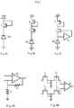
- Figs.3A to 3C show the structures of the light intensity detector 210.
- the light intensity detector 210 includes a photodiode PD 1 whose anode is grounded, and a first transistor T 1 , a source electrode of which is connected to a cathode of the photodiode PD 1 , and a drain electrode and a gate electrode of which are connected to a power source VDD.
- the photodiode PD 1 may generate a current I upon the receipt of the optical signal. Based on this, there is a linear relationship between lnI and a change in a voltage generated between the source electrode and the gate electrode of the first transistor T 1 .
- the first electric signal from the light intensity detector is in logarithmic relation with the intensity of the received optical signal.
- the light intensity detector 210 includes a photodiode PD 1 whose anode is grounded, a first transistor T 1 and a second transistor T 2 .
- a source electrode of the first transistor T 1 is connected to the power source VDD, a gate electrode and a drain electrode thereof are connected to a drain electrode of the second transistor T 2 , and a source electrode of the second transistor T 2 is connected to a cathode of the photodiode PD 1 .
- the light intensity detector 210 includes a photodiode PD 1 whose anode is grounded, N transistors connected to each other in series (N ⁇ 2), and a first amplifier A 1 .
- a source electrode of a first transistor is connected to a cathode of the photodiode PD 1
- a source electrode of an N th transistor is connected to the power source VDD
- a drain electrode of each of a second to the N th transistors is connected to a source electrode of a previous transistor
- a gate electrode of each of the second to the N th transistors is connected to a drain electrode of the previous transistor.
- the first amplifier A 1 is connected between the cathode of the photodiode PD 1 and a gate electrode of the first transistor. Through the first amplifier A 1 , it is able for the pixel collection circuit to detect the light intensity change in a more rapid manner.
- the light intensity detector may also be any well-known highly real-time photoelectric detector, which will not be particularly defined herein. It should be appreciated that, for a conventional photoelectric detection technology, usually a capacitor needs to be charged, then the light intensity detector needs to be exposed continuously (i.e., the capacitor needs to be discharged continuously), and then an accumulated light intensity may be determined in accordance with a remaining capacity of the capacitor. In the embodiments of the present disclosure, it is unnecessary to expose the light intensity detector 210 when the first electric signal representing the intensity of the optical signal has been generated by the light intensity detector 210, so it is able for the light intensity detector 210 to output the first electric signal without any delay.
- the light intensity change amplifier 260 is configured to preprocess the first electric signal so as to generate a second electric signal.
- the preprocessing may include the isolation of a direct current component and the amplification of an alternating current component, so as to amplify the first electric signal.
- the light intensity change amplifier 260 it is able to increase the light intensity detection sensitivity of the pixel collection circuit 200.
- the light intensity change amplifier 260 may be a switched-capacitor amplification circuit, which is configured to isolate the direct current component of an output voltage from the light intensity detector 210, and provide a gain for the alternating current component through setting a ratio between capacitances of two capacitors.
- the light intensity change amplifier 260 may be a resistance-feedback amplifier or a correlated double sampling circuit. Figs.4A to 4C show the structures of the light intensity change amplifier 260.
- the light intensity change amplifier 260 includes a second amplifier A 2 , a first resistor R 1 and a second resistor R 2 .
- a positive pole of the second amplifier A2 is connected to the output end of the light intensity detector 210, a negative pole thereof is connected to the first pull-down resistor R 1 , and the second resistor R 2 is connected between an output end and the negative pole of the second amplifier A 2 .
- the light intensity change amplifier 260 may be the correlated double sampling circuit, which may include: a third transistor T 3 , a drain electrode of which is connected to the output end of the light intensity detector 210; a fourth transistor T 4 , a drain electrode of which is connected to the output end of the light intensity detector 210; a first capacitor C 1 , a first end of which is connected to a source electrode of the third transistor T 3 , and a second end of which is grounded; a second capacitor C 2 , a first end of which is connected to a source electrode of the fourth transistor T 4 , and a second end of which is grounded; a fifth transistor T 5 , a drain electrode of which is connected to the first end of the first capacitor C 1 ; a sixth transistor T 6 , a gate electrode of which is connected to a gate electrode of the fifth transistor, and a drain electrode of which is connected to the first end of the second capacitor C 2 ; and a third amplifier A 3 , a positive pole of which is
- the transistors of the light intensity change amplifier 260 may be turned off.
- T 3 may be turned on, so as to sample a to-be-sampled voltage to the capacitor C 1 , and after a sampling time period, T 1 may be turned off.
- T 4 may be turned on, so as to sample a to-be-sampled voltage to the capacitor C 2 , and after the sampling time period, T 4 may be turned off.
- T 5 may be turned on, and the third amplifier A 3 may amplify a voltage difference between the positive and negative poles and output a voltage.
- the light intensity change amplifier 260 includes a fourth amplifier A 4 , a third capacitor C 3 , a fourth capacitor C 4 and a first switch K 1 .
- a first end of the third capacitor C 3 is connected to the output end of the light intensity detector 210, a negative pole of the fourth amplifier A 4 is configured to receive a fixed potential, a positive pole of the fourth amplifier A 4 is connected to a second end of the third capacitor C 3 , and the fourth capacitor C 4 and the first switch K 1 are connected in parallel between the positive pole and an output end of the fourth amplifier A 4 .
- the first switch K 1 may be switched on.
- the light intensity change amplifier 260 may also be any other known light intensity change amplifier, which also falls within the scope of the present disclosure and thus will not be particularly defined herein.
- the dual-threshold filter 270 is configured to determine whether a change of the first electric signal processed by the light intensity change amplifier 260 (i.e., the second electric signal) meets a predetermined condition.
- the dual-threshold filter 270 may be a continuous time comparator. Through setting a positive threshold and a negative threshold, it is able to determine whether the light intensity increases or decreases.
- the dual-threshold filter 270 may be configured to determine whether the second electric signal is smaller than the negative threshold or greater than the positive threshold through two voltage comparators, and when the second electric signal is smaller than the negative threshold or greater than the positive threshold, determine that the change of the second electric signal meets the predetermined condition.
- each pixel unit may be in one of the following states, i.e., the initiatively-activated state, the passively-activated state and the nonactivated state.
- the initiatively-activated state and the passively-activated state may be collectively called as an activated state.
- the first state storage module 220 is configured to store therein the initiatively-activated state and the nonactivated state of the pixel unit
- the second state storage module 230 is configured to store therein the passively-activated state and the nonactivated state of the pixel unit.
- the pixel unit When the change of the first electric signal processed by the dual-threshold filter 270 (i.e., the second electric signal) meets the predetermined condition, the pixel unit may be triggered to be in the initiatively-activated state, and at this time, the first state storage module 220 may store the initiatively-activated state.
- the pixel collection circuit may communicate with an adjacent pixel collection circuit through the first state storage module 220.
- the first state storage module 220 may transmit the row request signal to each row request line in the initiatively-activated state.
- the pixel row signal communication unit 120 of the optical flow sensor may randomly respond to one of the row request signals for the plurality of rows of pixel collection circuits.
- a second input end of the first state storage module 220 may be coupled to a row response line, and a third input end thereof may be coupled to a column response line.
- the activated state i.e., the initiatively-activated state or the passively-activated state
- the first state storage module 220 may transmit the column request signal to the column request line, notify the light intensity signal collection and storage module 240 to output the first electric signal as the light intensity signal, and notify the time information module 260 to output the corresponding time signal.
- the first state storage module 220 may transmit the pulse signal to at least one adjacent pixel collection circuit in the activated state, so as to enable the at least one adjacent pixel collection circuit to be in the passively-activated state.
- the first state storage module 220 in the activated state may transmit the pulse signal to four pixel units, i.e., an upper pixel unit, a lower pixel unit, a left pixel unit and a right pixel unit, so as to enable these pixel units to be in the passively-activated state.
- the first state storage module 220 may be configured to deactivate the pixel collection circuit, i.e., enable the pixel collection circuit to be in the nonactivated state, upon the receipt of the row response signal from the row response line and the column response signal from the column response line simultaneously.
- a third output end of the first state storage module 220 is coupled to the light intensity change amplifier 260, and when the pixel collection circuit is in the activated state or the nonactivated state, transmits a resetting signal to the light intensity change amplifier 260.
- the first state storage module 220 includes a first latch configured to store the activated state and the nonactivated state.
- the first latch When the second electric signal meets the predetermined condition, the first latch may be set, i.e., the pixel unit may be in the activated state. When both the row response signal and the column response signal have bene received simultaneously, the first latch may be reset, i.e., the pixel unit may be in the nonactivated state. Each time when the first latch is set or reset, the first state storage module may transmit the resetting signal to the light intensity change amplifier 260.
- the pixel unit may be in the passively-activated state, and at this time, the second state storage module 230 may store the passively-activated state.
- the pixel units may communicate with each other through the second state storage module 230.
- each pixel unit may communicate with four pixel units, i.e., an upper pixel unit, a lower pixel unit, a left pixel unit and a right pixel unit.
- the pixel unit may be in the passively-activated state, and may not transmit the pulse signal to the other pixel unit.
- the pixel unit in the passively-activated state may detect the light intensity change continuously, and prior to the reception of the row response signal, it may also be triggered to be in the initiatively-activated state.
- the second state storage module 230 may transmit a notification to the first state storage module 220, so as to enable the first state storage module in the activated state to transmit the row request signal to each row request line.
- the pixel row signal communication unit 120 of the optical flow sensor may randomly respond to one of the row request signals for the plurality of rows of pixel collection circuits.
- a second input end of the second state storage module 230 is coupled to the row response line, and a third input end thereof is coupled to the column response line (not shown in Fig.2 ).
- the first state storage module 220 may transmit the column request signal to the column request line, notify the light intensity signal collection and storage module 240 to output the first electric signal as the light intensity signal, and notify the time information module 260 to output the corresponding time signal.
- the second state storage module 230 may also be directly coupled to the first state storage module 220.
- the second state storage module 230 may receive, through the first state storage module 220, the row response signal from the row response line and the column response signal from the column response line.
- the modules may be directly connected to the row response line and/or the column response line so as to acquire the corresponding response signal, or the corresponding response signal may be cached in the first state storage module 220 and then transmitted to these modules (e.g., the second state storage module 230, the light intensity signal collection and storage module 240, and the time information storage module 250), which will not be particularly defined herein.
- the pixel unit when the second state storage module 230 has received the row response signal from the row response line and the column response signal from the column response line simultaneously, the pixel unit may be deactivated, and the second state storage module 230 may transmit, through the first state storage module 220, the resetting signal to the light intensity change amplifier 260.
- the second state storage module 230 may include a second latch configured to store the passively-activated state and the nonactivated state. Upon the receipt of the pulse signal from the at least one adjacent pixel collection circuit, the second latch may be set, and the pixel unit may be in the passively-activated state.
- the second latch may be reset, and the pixel unit may be in the nonactivated state.
- the second state storage module 230 may transmit the resetting signal to the light intensity change amplifier 260.
- the light intensity signal collection and storage module 240 may store and output the first electric signal as the light intensity signal in accordance with the state of the pixel collection circuit.
- the light intensity signal collection and storage module 240 may sample in real time the first electric signal.
- the light intensity signal collection and storage module 240 may store the sampled first electric signal, until it has received the row response signal from the first state storage module 220 or the second state storage module 230. Then, the light intensity signal collection and storage module 240 may output the stored first electric signal as the light intensity signal.
- the time information storage module 250 may store and output the corresponding time signal in accordance with the state of the pixel collection circuit.
- the time information storage module 250 may sample in real time the first time signal from the time signal line.
- the time information storage module 250 may store the sampled first time signal, until it has received the row response signal from the first state storage module 220 or the second state storage module 230. Then, the time information storage module 250 may output the stored first time signal as the time signal.
- each pixel collection circuit in the pixel collection circuit array of the optical flow sensor may detect in real time a light intensity change in a field of vision, and when the light intensity change meets the predetermined condition, the pixel collection circuit may be triggered to be in the initiatively-activated state.
- the pixel collection circuit in the initiatively-activated state may transmit the pulse signal to four or more pixel collection circuits surrounding the pixel collection circuit, so as to enable the adjacent pixel collection circuits in a deactivated state to be in the passively-activated state.
- light intensity information and time information about this pixel collection circuit and the passively-activated pixel collection circuits may be sampled, stored and output to an image collection system.
- the optical flow sensor in the embodiments of the present disclosure, it is able to collect a light intensity of a corresponding pixel point of a target object in the field of vision at a certain moment, light intensities of the pixel points surrounding the pixel point, and light intensities of the same pixel point at different moments, thereby to acquire parameters of an optical flow constraint equation for an optical flow algorithm, i.e., a time-domain gradient value and a space-domain gradient value of the pixel point.
- modules, units or components in the above examples may be arranged in the device described in the embodiments, or in one or more devices different from the device.
- the modules may be combined into one module, or each module may be divided into a plurality of submodules.
- the modules may be modified adaptively and arranged in one or more devices different from that mentioned hereinabove.
- the modules, units or components may be combined into one module, unit or component, or each module, unit or component may be divided into a plurality of submodules, subunits or subcomponents.
- all the features, processes or units involved in the specification may be combined in any form. Unless otherwise defined, each feature in the specification (including the appended claims, abstract and drawings) may be replaced with a same, equivalent or similar feature.
- A8 The pixel collection circuit according to A7, wherein the second state storage module includes a second latch configured to be set upon the receipt of the pulse signal from at least one adjacent pixel collection circuit, and reset upon the receipt of the row response signal and the column response signal simultaneously, wherein the second state storage module is further configured to transmit the resetting signal to the light intensity change amplifier when the second latch has been reset.
- the second state storage module includes a second latch configured to be set upon the receipt of the pulse signal from at least one adjacent pixel collection circuit, and reset upon the receipt of the row response signal and the column response signal simultaneously, wherein the second state storage module is further configured to transmit the resetting signal to the light intensity change amplifier when the second latch has been reset.
- A9 The pixel collection circuit according to any one of A2 to A8, wherein the preprocessing includes the isolation of the direct current component and the amplification of the alternating current component.
- the pixel collection circuit according to any one of A1 to A9, wherein the light intensity detector includes: a photodiode PD 1 whose anode is grounded; and a first transistor T 1 , a source electrode of which is connected to a cathode of the photodiode PD 1 , and a drain electrode and a gate electrode of which are connected to a power source VDD.
- the pixel collection circuit according to any one of A1 to A9, wherein the light intensity detector includes: a photodiode PD 1 whose anode is grounded; a first transistor T 1 , a source electrode of which is connected to a power source VDD; and a second transistor T 2 , a source electrode of which is connected to a cathode of the photodiode PD 1 , and a drain electrode of which is connected to a gate electrode and a drain electrode of the first transistor T 1 .
- the light intensity detector includes: a photodiode PD 1 whose anode is grounded; N transistors connected in series, N ⁇ 2, a source electrode of a first transistor being connected to a cathode of the photodiode PD 1 , a source electrode of an N th transistor being connected to a power source VDD, a drain electrode of each of a second to the N th transistors being connected to a source electrode of a previous transistor, a gate electrode of each of the second to the N th transistors being connected to a drain electrode of the previous transistor; and a first amplifier A 1 connected between the cathode of the photodiode PD 1 and a gate electrode of the first transistor.
- A13 The pixel collection circuit according to any one of A2 to A12, wherein the light intensity change amplifier includes a second amplifier A 2 , a positive pole of which is connected to an output end of the light intensity detector, and a negative pole of which is connected to a first pull-down resistor R 1 , wherein a second resistor R 2 is connected between an output end and the negative pole of the second amplifier, and the second amplifier is configured to preprocess the first electric signal from the light intensity detector.
- the light intensity change amplifier includes a second amplifier A 2 , a positive pole of which is connected to an output end of the light intensity detector, and a negative pole of which is connected to a first pull-down resistor R 1 , wherein a second resistor R 2 is connected between an output end and the negative pole of the second amplifier, and the second amplifier is configured to preprocess the first electric signal from the light intensity detector.
- the light intensity change amplifier includes: a third transistor T 3 , a drain electrode of which is connected to the output end of the light intensity detector; a fourth transistor T 4 , a drain electrode of which is connected to the output end of the light intensity detector; a first capacitor C 1 , a first end of which is connected to a source electrode of the third transistor T 3 , and a second end of which is grounded; a second capacitor C 2 , a first end of which is connected to a source electrode of the fourth transistor T 4 , and a second end of which is grounded; a fifth transistor T 5 , a drain electrode of which is connected to the first end of the first capacitor C 1 ; a sixth transistor T 6 , a gate electrode of which is connected to a gate electrode of the fifth transistor T 5 , and a drain electrode of which is connected to the first end of the second capacitor C 2 ; and a third amplifier A 3 , a positive pole of which is connected to a third transistor T 3 , a drain electrode of which is connected to the output end of
Landscapes
- Engineering & Computer Science (AREA)
- Multimedia (AREA)
- Signal Processing (AREA)
- Physics & Mathematics (AREA)
- General Physics & Mathematics (AREA)
- Spectroscopy & Molecular Physics (AREA)
- Transforming Light Signals Into Electric Signals (AREA)
- Photometry And Measurement Of Optical Pulse Characteristics (AREA)
Applications Claiming Priority (2)
| Application Number | Priority Date | Filing Date | Title |
|---|---|---|---|
| CN201810380023.8A CN108827461B (zh) | 2018-04-25 | 2018-04-25 | 像素采集电路及光流传感器 |
| PCT/CN2018/088260 WO2019205217A1 (zh) | 2018-04-25 | 2018-05-24 | 像素采集电路及光流传感器 |
Publications (3)
| Publication Number | Publication Date |
|---|---|
| EP3761631A1 true EP3761631A1 (de) | 2021-01-06 |
| EP3761631A4 EP3761631A4 (de) | 2022-01-05 |
| EP3761631B1 EP3761631B1 (de) | 2023-04-12 |
Family
ID=64154904
Family Applications (1)
| Application Number | Title | Priority Date | Filing Date |
|---|---|---|---|
| EP18916050.0A Active EP3761631B1 (de) | 2018-04-25 | 2018-05-24 | Pixelerfassungsschaltung und optischer flusssensor |
Country Status (6)
| Country | Link |
|---|---|
| US (1) | US11122232B2 (de) |
| EP (1) | EP3761631B1 (de) |
| JP (1) | JP7099783B2 (de) |
| CN (1) | CN108827461B (de) |
| SG (1) | SG11202009813XA (de) |
| WO (1) | WO2019205217A1 (de) |
Families Citing this family (10)
| Publication number | Priority date | Publication date | Assignee | Title |
|---|---|---|---|---|
| CN108449557B (zh) * | 2018-03-23 | 2019-02-15 | 上海芯仑光电科技有限公司 | 像素采集电路、光流传感器和光流及图像信息采集系统 |
| WO2020100663A1 (ja) | 2018-11-16 | 2020-05-22 | ソニーセミコンダクタソリューションズ株式会社 | 固体撮像装置及び撮像装置 |
| US11521998B2 (en) * | 2018-09-18 | 2022-12-06 | Sony Semiconductor Solutions Corporation | Solid-state imaging device and imaging device |
| JP2020088722A (ja) * | 2018-11-29 | 2020-06-04 | ソニーセミコンダクタソリューションズ株式会社 | 固体撮像素子、および、撮像装置 |
| CN109842767B (zh) * | 2019-01-09 | 2020-07-14 | 上海芯仑光电科技有限公司 | 一种防闪光电路组件及图像传感器 |
| CN109842768B (zh) * | 2019-01-29 | 2020-05-15 | 上海芯仑光电科技有限公司 | 一种像素采集电路及图像传感器 |
| KR102747641B1 (ko) | 2019-06-26 | 2024-12-27 | 삼성전자주식회사 | 비전 센서, 이를 포함하는 이미지 처리 장치 및 비전 센서의 동작 방법 |
| CN110536083B (zh) | 2019-08-30 | 2020-11-06 | 上海芯仑光电科技有限公司 | 一种图像传感器及图像采集系统 |
| CN111107287B (zh) * | 2019-11-29 | 2021-06-04 | 豪威芯仑传感器(上海)有限公司 | 一种像素采集电路及图像传感器 |
| US11516419B2 (en) | 2021-01-22 | 2022-11-29 | Omnivision Technologies, Inc. | Digital time stamping design for event driven pixel |
Family Cites Families (22)
| Publication number | Priority date | Publication date | Assignee | Title |
|---|---|---|---|---|
| US6253161B1 (en) * | 1997-07-10 | 2001-06-26 | Universite Laval | Integrated motion vision sensor |
| JP3449468B2 (ja) * | 1999-05-06 | 2003-09-22 | 日本電気株式会社 | 固体撮像装置およびその駆動方法 |
| US8553943B2 (en) * | 2011-06-14 | 2013-10-08 | Qualcomm Incorporated | Content-adaptive systems, methods and apparatus for determining optical flow |
| KR20140056986A (ko) * | 2012-11-02 | 2014-05-12 | 삼성전자주식회사 | 모션 센서 어레이 장치, 상기 모선 센서 어레이를 이용한 거리 센싱 시스템, 및 거리 센싱 방법 |
| US9852512B2 (en) * | 2013-03-13 | 2017-12-26 | Electronic Scripting Products, Inc. | Reduced homography based on structural redundancy of conditioned motion |
| KR102347249B1 (ko) * | 2014-10-21 | 2022-01-04 | 삼성전자주식회사 | 외부 물체의 움직임과 연관된 이벤트에 응답하여 화면을 디스플레이하는 장치 및 방법 |
| KR102248404B1 (ko) * | 2014-11-17 | 2021-05-07 | 삼성전자주식회사 | 움직임 분석 방법 및 움직임 분석 장치 |
| CN104535077A (zh) * | 2014-12-29 | 2015-04-22 | 上海交通大学 | 一种基于智能移动终端设备的行人步长估计方法 |
| WO2016164342A1 (en) * | 2015-04-06 | 2016-10-13 | Scope Technologies Us Inc. | Methods and apparatus for augmented reality applications |
| US9743024B2 (en) * | 2015-07-01 | 2017-08-22 | Massachusetts Institute Of Technology | Method and apparatus for on-chip per-pixel pseudo-random time coded exposure |
| FR3039319B1 (fr) * | 2015-07-24 | 2018-06-15 | Pyxalis | Capteur d'image a pixels actifs avec fonctionnement en mode d'obturateur global, soustraction du bruit de reinitialisation et lecture non destructive |
| KR102421141B1 (ko) * | 2015-10-30 | 2022-07-14 | 삼성전자주식회사 | 이벤트 신호 및 영상의 저장 방법 및 저장 장치, 저장 장치로 이벤트 신호를 전송하는 비전 센서의 동작 방법 |
| CN106027896A (zh) * | 2016-06-20 | 2016-10-12 | 零度智控(北京)智能科技有限公司 | 视频拍摄控制装置、方法及无人机 |
| CN106162000B (zh) * | 2016-07-08 | 2019-03-15 | 上海芯仑光电科技有限公司 | 像素采集电路、图像传感器及图像采集系统 |
| EP3267678B1 (de) * | 2016-07-08 | 2022-10-05 | OmniVision Sensor Solution (Shanghai) Co., Ltd | Pixelerfassungsschaltung, bildsensor und bilderfassungssystem |
| CN106097699B (zh) * | 2016-07-25 | 2022-05-20 | 深圳市冠旭电子股份有限公司 | 一种光控装置和光控系统 |
| KR102720734B1 (ko) * | 2016-08-02 | 2024-10-22 | 삼성전자주식회사 | 이벤트 신호 처리 방법 및 장치 |
| WO2018122798A1 (en) * | 2016-12-30 | 2018-07-05 | Insightness Ag | Dynamic vision sensor architecture |
| CN108700664A (zh) * | 2017-02-06 | 2018-10-23 | 松下知识产权经营株式会社 | 三维运动取得装置及三维运动取得方法 |
| CN108632546B (zh) * | 2017-03-17 | 2021-06-04 | 豪威芯仑传感器(上海)有限公司 | 像素采集电路、光流传感器及图像采集系统 |
| CN107147856B (zh) * | 2017-03-30 | 2019-11-22 | 深圳大学 | 一种像素单元及其去噪方法、动态视觉传感器、成像装置 |
| US10706564B2 (en) * | 2018-04-11 | 2020-07-07 | Wisconsin Alumni Research Foundation | Systems, methods, and media for determining object motion in three dimensions from light field image data |
-
2018
- 2018-04-25 CN CN201810380023.8A patent/CN108827461B/zh active Active
- 2018-05-24 WO PCT/CN2018/088260 patent/WO2019205217A1/zh not_active Ceased
- 2018-05-24 SG SG11202009813XA patent/SG11202009813XA/en unknown
- 2018-05-24 EP EP18916050.0A patent/EP3761631B1/de active Active
- 2018-05-24 JP JP2020552018A patent/JP7099783B2/ja active Active
-
2020
- 2020-09-24 US US17/030,864 patent/US11122232B2/en active Active
Also Published As
| Publication number | Publication date |
|---|---|
| EP3761631A4 (de) | 2022-01-05 |
| CN108827461A (zh) | 2018-11-16 |
| US20210037202A1 (en) | 2021-02-04 |
| JP7099783B2 (ja) | 2022-07-12 |
| CN108827461B (zh) | 2019-05-03 |
| US11122232B2 (en) | 2021-09-14 |
| SG11202009813XA (en) | 2020-11-27 |
| WO2019205217A1 (zh) | 2019-10-31 |
| JP2021520699A (ja) | 2021-08-19 |
| EP3761631B1 (de) | 2023-04-12 |
Similar Documents
| Publication | Publication Date | Title |
|---|---|---|
| US11122232B2 (en) | Pixel collection circuit and optical flow sensor | |
| US12022211B1 (en) | Pixel collection circuit, optical flow sensor, and optical flow and image information collection system | |
| US9635287B2 (en) | Method and apparatus for integrated sensor to provide higher resolution, lower frame rate and lower resolution, higher frame rate imagery simultaneously | |
| US11869273B2 (en) | Object recognition with removal of event as noise when the event is detected for a group of pixels exceeding a threshold | |
| US10181194B2 (en) | Pixel acquisition circuit, optical flow sensor, and image acquisition system | |
| US9128195B2 (en) | Increasing dynamic range for x-ray image sensor | |
| EP2728373A1 (de) | Verbesserungen bei Flugzeitpixelschaltungen | |
| US11815394B2 (en) | Photoelectric conversion device, method of controlling photoelectric conversion device, and information processing apparatus | |
| EP3267678B1 (de) | Pixelerfassungsschaltung, bildsensor und bilderfassungssystem | |
| EP3376754B1 (de) | Pixel-erfassungsschaltung, optischer durchfluss-sensor, und bildübernahmesystem | |
| CN112738365B (zh) | 成像设备和信息处理系统 | |
| US20130182075A1 (en) | Geospatial and image data collection system including image sensor for capturing 3d geospatial data and 2d image data and related methods | |
| WO2025026636A1 (en) | 2d tdc arrangement | |
| CN109584278B (zh) | 一种目标识别装置及方法 | |
| US10955551B2 (en) | Pixel output processing circuit with laser range finding (LRF) capability | |
| IL269841B1 (en) | Sensors for simultaneous passive imaging and range finding | |
| US20180227508A1 (en) | Event-triggered imaging pixels | |
| CN120937387A (zh) | 固体摄像装置 | |
| WO2023119934A1 (ja) | 閾値決定方法、閾値決定プログラム、閾値決定装置、光子数識別システム、光子数識別方法および光子数識別処理プログラム | |
| CN119618385A (zh) | 红外焦平面探测器的测试系统、方法、设备及存储介质 | |
| CN120428195A (zh) | 信号处理的装置、方法和系统 |
Legal Events
| Date | Code | Title | Description |
|---|---|---|---|
| STAA | Information on the status of an ep patent application or granted ep patent |
Free format text: STATUS: THE INTERNATIONAL PUBLICATION HAS BEEN MADE |
|
| PUAI | Public reference made under article 153(3) epc to a published international application that has entered the european phase |
Free format text: ORIGINAL CODE: 0009012 |
|
| STAA | Information on the status of an ep patent application or granted ep patent |
Free format text: STATUS: REQUEST FOR EXAMINATION WAS MADE |
|
| 17P | Request for examination filed |
Effective date: 20200929 |
|
| AK | Designated contracting states |
Kind code of ref document: A1 Designated state(s): AL AT BE BG CH CY CZ DE DK EE ES FI FR GB GR HR HU IE IS IT LI LT LU LV MC MK MT NL NO PL PT RO RS SE SI SK SM TR |
|
| AX | Request for extension of the european patent |
Extension state: BA ME |
|
| RAP3 | Party data changed (applicant data changed or rights of an application transferred) |
Owner name: OMNIVISION SENSOR SOLUTION (SHANGHAI) CO., LTD |
|
| DAV | Request for validation of the european patent (deleted) | ||
| DAX | Request for extension of the european patent (deleted) | ||
| REG | Reference to a national code |
Ref country code: DE Ref legal event code: R079 Ref document number: 602018048455 Country of ref document: DE Free format text: PREVIOUS MAIN CLASS: H04N0005345000 Ipc: H04N0005374500 |
|
| A4 | Supplementary search report drawn up and despatched |
Effective date: 20211207 |
|
| RIC1 | Information provided on ipc code assigned before grant |
Ipc: H04N 5/3745 20110101AFI20211201BHEP |
|
| GRAP | Despatch of communication of intention to grant a patent |
Free format text: ORIGINAL CODE: EPIDOSNIGR1 |
|
| STAA | Information on the status of an ep patent application or granted ep patent |
Free format text: STATUS: GRANT OF PATENT IS INTENDED |
|
| INTG | Intention to grant announced |
Effective date: 20221213 |
|
| GRAS | Grant fee paid |
Free format text: ORIGINAL CODE: EPIDOSNIGR3 |
|
| GRAA | (expected) grant |
Free format text: ORIGINAL CODE: 0009210 |
|
| STAA | Information on the status of an ep patent application or granted ep patent |
Free format text: STATUS: THE PATENT HAS BEEN GRANTED |
|
| AK | Designated contracting states |
Kind code of ref document: B1 Designated state(s): AL AT BE BG CH CY CZ DE DK EE ES FI FR GB GR HR HU IE IS IT LI LT LU LV MC MK MT NL NO PL PT RO RS SE SI SK SM TR |
|
| REG | Reference to a national code |
Ref country code: GB Ref legal event code: FG4D |
|
| REG | Reference to a national code |
Ref country code: CH Ref legal event code: EP |
|
| REG | Reference to a national code |
Ref country code: DE Ref legal event code: R096 Ref document number: 602018048455 Country of ref document: DE |
|
| REG | Reference to a national code |
Ref country code: IE Ref legal event code: FG4D |
|
| REG | Reference to a national code |
Ref country code: AT Ref legal event code: REF Ref document number: 1560432 Country of ref document: AT Kind code of ref document: T Effective date: 20230515 |
|
| REG | Reference to a national code |
Ref country code: LT Ref legal event code: MG9D |
|
| REG | Reference to a national code |
Ref country code: NL Ref legal event code: MP Effective date: 20230412 |
|
| REG | Reference to a national code |
Ref country code: AT Ref legal event code: MK05 Ref document number: 1560432 Country of ref document: AT Kind code of ref document: T Effective date: 20230412 |
|
| PG25 | Lapsed in a contracting state [announced via postgrant information from national office to epo] |
Ref country code: NL Free format text: LAPSE BECAUSE OF FAILURE TO SUBMIT A TRANSLATION OF THE DESCRIPTION OR TO PAY THE FEE WITHIN THE PRESCRIBED TIME-LIMIT Effective date: 20230412 |
|
| PG25 | Lapsed in a contracting state [announced via postgrant information from national office to epo] |
Ref country code: SE Free format text: LAPSE BECAUSE OF FAILURE TO SUBMIT A TRANSLATION OF THE DESCRIPTION OR TO PAY THE FEE WITHIN THE PRESCRIBED TIME-LIMIT Effective date: 20230412 Ref country code: PT Free format text: LAPSE BECAUSE OF FAILURE TO SUBMIT A TRANSLATION OF THE DESCRIPTION OR TO PAY THE FEE WITHIN THE PRESCRIBED TIME-LIMIT Effective date: 20230814 Ref country code: NO Free format text: LAPSE BECAUSE OF FAILURE TO SUBMIT A TRANSLATION OF THE DESCRIPTION OR TO PAY THE FEE WITHIN THE PRESCRIBED TIME-LIMIT Effective date: 20230712 Ref country code: ES Free format text: LAPSE BECAUSE OF FAILURE TO SUBMIT A TRANSLATION OF THE DESCRIPTION OR TO PAY THE FEE WITHIN THE PRESCRIBED TIME-LIMIT Effective date: 20230412 Ref country code: AT Free format text: LAPSE BECAUSE OF FAILURE TO SUBMIT A TRANSLATION OF THE DESCRIPTION OR TO PAY THE FEE WITHIN THE PRESCRIBED TIME-LIMIT Effective date: 20230412 |
|
| PG25 | Lapsed in a contracting state [announced via postgrant information from national office to epo] |
Ref country code: RS Free format text: LAPSE BECAUSE OF FAILURE TO SUBMIT A TRANSLATION OF THE DESCRIPTION OR TO PAY THE FEE WITHIN THE PRESCRIBED TIME-LIMIT Effective date: 20230412 Ref country code: PL Free format text: LAPSE BECAUSE OF FAILURE TO SUBMIT A TRANSLATION OF THE DESCRIPTION OR TO PAY THE FEE WITHIN THE PRESCRIBED TIME-LIMIT Effective date: 20230412 Ref country code: LV Free format text: LAPSE BECAUSE OF FAILURE TO SUBMIT A TRANSLATION OF THE DESCRIPTION OR TO PAY THE FEE WITHIN THE PRESCRIBED TIME-LIMIT Effective date: 20230412 Ref country code: LT Free format text: LAPSE BECAUSE OF FAILURE TO SUBMIT A TRANSLATION OF THE DESCRIPTION OR TO PAY THE FEE WITHIN THE PRESCRIBED TIME-LIMIT Effective date: 20230412 Ref country code: IS Free format text: LAPSE BECAUSE OF FAILURE TO SUBMIT A TRANSLATION OF THE DESCRIPTION OR TO PAY THE FEE WITHIN THE PRESCRIBED TIME-LIMIT Effective date: 20230812 Ref country code: HR Free format text: LAPSE BECAUSE OF FAILURE TO SUBMIT A TRANSLATION OF THE DESCRIPTION OR TO PAY THE FEE WITHIN THE PRESCRIBED TIME-LIMIT Effective date: 20230412 Ref country code: GR Free format text: LAPSE BECAUSE OF FAILURE TO SUBMIT A TRANSLATION OF THE DESCRIPTION OR TO PAY THE FEE WITHIN THE PRESCRIBED TIME-LIMIT Effective date: 20230713 Ref country code: AL Free format text: LAPSE BECAUSE OF FAILURE TO SUBMIT A TRANSLATION OF THE DESCRIPTION OR TO PAY THE FEE WITHIN THE PRESCRIBED TIME-LIMIT Effective date: 20230412 |
|
| PG25 | Lapsed in a contracting state [announced via postgrant information from national office to epo] |
Ref country code: FI Free format text: LAPSE BECAUSE OF FAILURE TO SUBMIT A TRANSLATION OF THE DESCRIPTION OR TO PAY THE FEE WITHIN THE PRESCRIBED TIME-LIMIT Effective date: 20230412 |
|
| REG | Reference to a national code |
Ref country code: DE Ref legal event code: R097 Ref document number: 602018048455 Country of ref document: DE |
|
| PG25 | Lapsed in a contracting state [announced via postgrant information from national office to epo] |
Ref country code: SK Free format text: LAPSE BECAUSE OF FAILURE TO SUBMIT A TRANSLATION OF THE DESCRIPTION OR TO PAY THE FEE WITHIN THE PRESCRIBED TIME-LIMIT Effective date: 20230412 |
|
| PG25 | Lapsed in a contracting state [announced via postgrant information from national office to epo] |
Ref country code: MC Free format text: LAPSE BECAUSE OF FAILURE TO SUBMIT A TRANSLATION OF THE DESCRIPTION OR TO PAY THE FEE WITHIN THE PRESCRIBED TIME-LIMIT Effective date: 20230412 |
|
| REG | Reference to a national code |
Ref country code: BE Ref legal event code: MM Effective date: 20230531 |
|
| PG25 | Lapsed in a contracting state [announced via postgrant information from national office to epo] |
Ref country code: SM Free format text: LAPSE BECAUSE OF FAILURE TO SUBMIT A TRANSLATION OF THE DESCRIPTION OR TO PAY THE FEE WITHIN THE PRESCRIBED TIME-LIMIT Effective date: 20230412 Ref country code: SK Free format text: LAPSE BECAUSE OF FAILURE TO SUBMIT A TRANSLATION OF THE DESCRIPTION OR TO PAY THE FEE WITHIN THE PRESCRIBED TIME-LIMIT Effective date: 20230412 Ref country code: RO Free format text: LAPSE BECAUSE OF FAILURE TO SUBMIT A TRANSLATION OF THE DESCRIPTION OR TO PAY THE FEE WITHIN THE PRESCRIBED TIME-LIMIT Effective date: 20230412 Ref country code: MC Free format text: LAPSE BECAUSE OF FAILURE TO SUBMIT A TRANSLATION OF THE DESCRIPTION OR TO PAY THE FEE WITHIN THE PRESCRIBED TIME-LIMIT Effective date: 20230412 Ref country code: LU Free format text: LAPSE BECAUSE OF NON-PAYMENT OF DUE FEES Effective date: 20230524 Ref country code: EE Free format text: LAPSE BECAUSE OF FAILURE TO SUBMIT A TRANSLATION OF THE DESCRIPTION OR TO PAY THE FEE WITHIN THE PRESCRIBED TIME-LIMIT Effective date: 20230412 Ref country code: DK Free format text: LAPSE BECAUSE OF FAILURE TO SUBMIT A TRANSLATION OF THE DESCRIPTION OR TO PAY THE FEE WITHIN THE PRESCRIBED TIME-LIMIT Effective date: 20230412 Ref country code: CZ Free format text: LAPSE BECAUSE OF FAILURE TO SUBMIT A TRANSLATION OF THE DESCRIPTION OR TO PAY THE FEE WITHIN THE PRESCRIBED TIME-LIMIT Effective date: 20230412 |
|
| PLBE | No opposition filed within time limit |
Free format text: ORIGINAL CODE: 0009261 |
|
| STAA | Information on the status of an ep patent application or granted ep patent |
Free format text: STATUS: NO OPPOSITION FILED WITHIN TIME LIMIT |
|
| REG | Reference to a national code |
Ref country code: IE Ref legal event code: MM4A |
|
| 26N | No opposition filed |
Effective date: 20240115 |
|
| PG25 | Lapsed in a contracting state [announced via postgrant information from national office to epo] |
Ref country code: IE Free format text: LAPSE BECAUSE OF NON-PAYMENT OF DUE FEES Effective date: 20230524 |
|
| PG25 | Lapsed in a contracting state [announced via postgrant information from national office to epo] |
Ref country code: IE Free format text: LAPSE BECAUSE OF NON-PAYMENT OF DUE FEES Effective date: 20230524 |
|
| PG25 | Lapsed in a contracting state [announced via postgrant information from national office to epo] |
Ref country code: SI Free format text: LAPSE BECAUSE OF FAILURE TO SUBMIT A TRANSLATION OF THE DESCRIPTION OR TO PAY THE FEE WITHIN THE PRESCRIBED TIME-LIMIT Effective date: 20230412 |
|
| PG25 | Lapsed in a contracting state [announced via postgrant information from national office to epo] |
Ref country code: SI Free format text: LAPSE BECAUSE OF FAILURE TO SUBMIT A TRANSLATION OF THE DESCRIPTION OR TO PAY THE FEE WITHIN THE PRESCRIBED TIME-LIMIT Effective date: 20230412 Ref country code: IT Free format text: LAPSE BECAUSE OF FAILURE TO SUBMIT A TRANSLATION OF THE DESCRIPTION OR TO PAY THE FEE WITHIN THE PRESCRIBED TIME-LIMIT Effective date: 20230412 Ref country code: BE Free format text: LAPSE BECAUSE OF NON-PAYMENT OF DUE FEES Effective date: 20230531 |
|
| PG25 | Lapsed in a contracting state [announced via postgrant information from national office to epo] |
Ref country code: BG Free format text: LAPSE BECAUSE OF FAILURE TO SUBMIT A TRANSLATION OF THE DESCRIPTION OR TO PAY THE FEE WITHIN THE PRESCRIBED TIME-LIMIT Effective date: 20230412 |
|
| PG25 | Lapsed in a contracting state [announced via postgrant information from national office to epo] |
Ref country code: BG Free format text: LAPSE BECAUSE OF FAILURE TO SUBMIT A TRANSLATION OF THE DESCRIPTION OR TO PAY THE FEE WITHIN THE PRESCRIBED TIME-LIMIT Effective date: 20230412 |
|
| PGFP | Annual fee paid to national office [announced via postgrant information from national office to epo] |
Ref country code: DE Payment date: 20250513 Year of fee payment: 8 |
|
| PGFP | Annual fee paid to national office [announced via postgrant information from national office to epo] |
Ref country code: GB Payment date: 20250521 Year of fee payment: 8 |
|
| PGFP | Annual fee paid to national office [announced via postgrant information from national office to epo] |
Ref country code: FR Payment date: 20250530 Year of fee payment: 8 |
|
| PGFP | Annual fee paid to national office [announced via postgrant information from national office to epo] |
Ref country code: CH Payment date: 20250601 Year of fee payment: 8 |
|
| PG25 | Lapsed in a contracting state [announced via postgrant information from national office to epo] |
Ref country code: CY Free format text: LAPSE BECAUSE OF FAILURE TO SUBMIT A TRANSLATION OF THE DESCRIPTION OR TO PAY THE FEE WITHIN THE PRESCRIBED TIME-LIMIT; INVALID AB INITIO Effective date: 20180524 |
|
| PG25 | Lapsed in a contracting state [announced via postgrant information from national office to epo] |
Ref country code: HU Free format text: LAPSE BECAUSE OF FAILURE TO SUBMIT A TRANSLATION OF THE DESCRIPTION OR TO PAY THE FEE WITHIN THE PRESCRIBED TIME-LIMIT; INVALID AB INITIO Effective date: 20180524 |
|
| PG25 | Lapsed in a contracting state [announced via postgrant information from national office to epo] |
Ref country code: TR Free format text: LAPSE BECAUSE OF FAILURE TO SUBMIT A TRANSLATION OF THE DESCRIPTION OR TO PAY THE FEE WITHIN THE PRESCRIBED TIME-LIMIT Effective date: 20230412 |