EP3761772A1 - Procédé d'inspection de l'état de montage d'un composant, appareil d'inspection de carte de circuit imprimé et support d'enregistrement lisible par ordinateur - Google Patents
Procédé d'inspection de l'état de montage d'un composant, appareil d'inspection de carte de circuit imprimé et support d'enregistrement lisible par ordinateur Download PDFInfo
- Publication number
- EP3761772A1 EP3761772A1 EP19756511.2A EP19756511A EP3761772A1 EP 3761772 A1 EP3761772 A1 EP 3761772A1 EP 19756511 A EP19756511 A EP 19756511A EP 3761772 A1 EP3761772 A1 EP 3761772A1
- Authority
- EP
- European Patent Office
- Prior art keywords
- depth information
- component
- learning
- machine
- based model
- Prior art date
- Legal status (The legal status is an assumption and is not a legal conclusion. Google has not performed a legal analysis and makes no representation as to the accuracy of the status listed.)
- Granted
Links
Images


Classifications
-
- G—PHYSICS
- G06—COMPUTING OR CALCULATING; COUNTING
- G06T—IMAGE DATA PROCESSING OR GENERATION, IN GENERAL
- G06T7/00—Image analysis
- G06T7/0002—Inspection of images, e.g. flaw detection
- G06T7/0004—Industrial image inspection
-
- H—ELECTRICITY
- H05—ELECTRIC TECHNIQUES NOT OTHERWISE PROVIDED FOR
- H05K—PRINTED CIRCUITS; CASINGS OR CONSTRUCTIONAL DETAILS OF ELECTRIC APPARATUS; MANUFACTURE OF ASSEMBLAGES OF ELECTRICAL COMPONENTS
- H05K13/00—Apparatus or processes specially adapted for manufacturing or adjusting assemblages of electric components
- H05K13/08—Monitoring manufacture of assemblages
- H05K13/081—Integration of optical monitoring devices in assembly lines; Processes using optical monitoring devices specially adapted for controlling devices or machines in assembly lines
- H05K13/0817—Monitoring of soldering processes
-
- G—PHYSICS
- G01—MEASURING; TESTING
- G01B—MEASURING LENGTH, THICKNESS OR SIMILAR LINEAR DIMENSIONS; MEASURING ANGLES; MEASURING AREAS; MEASURING IRREGULARITIES OF SURFACES OR CONTOURS
- G01B11/00—Measuring arrangements characterised by the use of optical techniques
- G01B11/22—Measuring arrangements characterised by the use of optical techniques for measuring depth
-
- G—PHYSICS
- G01—MEASURING; TESTING
- G01B—MEASURING LENGTH, THICKNESS OR SIMILAR LINEAR DIMENSIONS; MEASURING ANGLES; MEASURING AREAS; MEASURING IRREGULARITIES OF SURFACES OR CONTOURS
- G01B11/00—Measuring arrangements characterised by the use of optical techniques
- G01B11/24—Measuring arrangements characterised by the use of optical techniques for measuring contours or curvatures
-
- G—PHYSICS
- G01—MEASURING; TESTING
- G01B—MEASURING LENGTH, THICKNESS OR SIMILAR LINEAR DIMENSIONS; MEASURING ANGLES; MEASURING AREAS; MEASURING IRREGULARITIES OF SURFACES OR CONTOURS
- G01B11/00—Measuring arrangements characterised by the use of optical techniques
- G01B11/24—Measuring arrangements characterised by the use of optical techniques for measuring contours or curvatures
- G01B11/25—Measuring arrangements characterised by the use of optical techniques for measuring contours or curvatures by projecting a pattern, e.g. one or more lines, moiré fringes on the object
- G01B11/2509—Color coding
-
- G—PHYSICS
- G01—MEASURING; TESTING
- G01N—INVESTIGATING OR ANALYSING MATERIALS BY DETERMINING THEIR CHEMICAL OR PHYSICAL PROPERTIES
- G01N21/00—Investigating or analysing materials by the use of optical means, i.e. using sub-millimetre waves, infrared, visible or ultraviolet light
- G01N21/84—Systems specially adapted for particular applications
- G01N21/88—Investigating the presence of flaws or contamination
- G01N21/8851—Scan or image signal processing specially adapted therefor, e.g. for scan signal adjustment, for detecting different kinds of defects, for compensating for structures, markings, edges
-
- G—PHYSICS
- G01—MEASURING; TESTING
- G01N—INVESTIGATING OR ANALYSING MATERIALS BY DETERMINING THEIR CHEMICAL OR PHYSICAL PROPERTIES
- G01N21/00—Investigating or analysing materials by the use of optical means, i.e. using sub-millimetre waves, infrared, visible or ultraviolet light
- G01N21/84—Systems specially adapted for particular applications
- G01N21/88—Investigating the presence of flaws or contamination
- G01N21/95—Investigating the presence of flaws or contamination characterised by the material or shape of the object to be examined
- G01N21/956—Inspecting patterns on the surface of objects
-
- G—PHYSICS
- G01—MEASURING; TESTING
- G01N—INVESTIGATING OR ANALYSING MATERIALS BY DETERMINING THEIR CHEMICAL OR PHYSICAL PROPERTIES
- G01N21/00—Investigating or analysing materials by the use of optical means, i.e. using sub-millimetre waves, infrared, visible or ultraviolet light
- G01N21/84—Systems specially adapted for particular applications
- G01N21/88—Investigating the presence of flaws or contamination
- G01N21/95—Investigating the presence of flaws or contamination characterised by the material or shape of the object to be examined
- G01N21/956—Inspecting patterns on the surface of objects
- G01N21/95684—Patterns showing highly reflecting parts, e.g. metallic elements
-
- G—PHYSICS
- G06—COMPUTING OR CALCULATING; COUNTING
- G06N—COMPUTING ARRANGEMENTS BASED ON SPECIFIC COMPUTATIONAL MODELS
- G06N3/00—Computing arrangements based on biological models
- G06N3/02—Neural networks
- G06N3/04—Architecture, e.g. interconnection topology
- G06N3/0464—Convolutional networks [CNN, ConvNet]
-
- G—PHYSICS
- G06—COMPUTING OR CALCULATING; COUNTING
- G06N—COMPUTING ARRANGEMENTS BASED ON SPECIFIC COMPUTATIONAL MODELS
- G06N3/00—Computing arrangements based on biological models
- G06N3/02—Neural networks
- G06N3/04—Architecture, e.g. interconnection topology
- G06N3/0475—Generative networks
-
- G—PHYSICS
- G06—COMPUTING OR CALCULATING; COUNTING
- G06N—COMPUTING ARRANGEMENTS BASED ON SPECIFIC COMPUTATIONAL MODELS
- G06N3/00—Computing arrangements based on biological models
- G06N3/02—Neural networks
- G06N3/08—Learning methods
-
- G—PHYSICS
- G06—COMPUTING OR CALCULATING; COUNTING
- G06N—COMPUTING ARRANGEMENTS BASED ON SPECIFIC COMPUTATIONAL MODELS
- G06N3/00—Computing arrangements based on biological models
- G06N3/02—Neural networks
- G06N3/08—Learning methods
- G06N3/09—Supervised learning
-
- G—PHYSICS
- G06—COMPUTING OR CALCULATING; COUNTING
- G06N—COMPUTING ARRANGEMENTS BASED ON SPECIFIC COMPUTATIONAL MODELS
- G06N3/00—Computing arrangements based on biological models
- G06N3/02—Neural networks
- G06N3/08—Learning methods
- G06N3/094—Adversarial learning
-
- G—PHYSICS
- G06—COMPUTING OR CALCULATING; COUNTING
- G06T—IMAGE DATA PROCESSING OR GENERATION, IN GENERAL
- G06T5/00—Image enhancement or restoration
- G06T5/60—Image enhancement or restoration using machine learning, e.g. neural networks
-
- G—PHYSICS
- G06—COMPUTING OR CALCULATING; COUNTING
- G06T—IMAGE DATA PROCESSING OR GENERATION, IN GENERAL
- G06T5/00—Image enhancement or restoration
- G06T5/70—Denoising; Smoothing
-
- G—PHYSICS
- G06—COMPUTING OR CALCULATING; COUNTING
- G06T—IMAGE DATA PROCESSING OR GENERATION, IN GENERAL
- G06T7/00—Image analysis
- G06T7/50—Depth or shape recovery
- G06T7/521—Depth or shape recovery from laser ranging, e.g. using interferometry; from the projection of structured light
-
- G—PHYSICS
- G06—COMPUTING OR CALCULATING; COUNTING
- G06T—IMAGE DATA PROCESSING OR GENERATION, IN GENERAL
- G06T7/00—Image analysis
- G06T7/50—Depth or shape recovery
- G06T7/55—Depth or shape recovery from multiple images
- G06T7/586—Depth or shape recovery from multiple images from multiple light sources, e.g. photometric stereo
-
- H—ELECTRICITY
- H04—ELECTRIC COMMUNICATION TECHNIQUE
- H04N—PICTORIAL COMMUNICATION, e.g. TELEVISION
- H04N23/00—Cameras or camera modules comprising electronic image sensors; Control thereof
- H04N23/56—Cameras or camera modules comprising electronic image sensors; Control thereof provided with illuminating means
-
- H—ELECTRICITY
- H04—ELECTRIC COMMUNICATION TECHNIQUE
- H04N—PICTORIAL COMMUNICATION, e.g. TELEVISION
- H04N23/00—Cameras or camera modules comprising electronic image sensors; Control thereof
- H04N23/90—Arrangement of cameras or camera modules, e.g. multiple cameras in TV studios or sports stadiums
-
- H—ELECTRICITY
- H05—ELECTRIC TECHNIQUES NOT OTHERWISE PROVIDED FOR
- H05K—PRINTED CIRCUITS; CASINGS OR CONSTRUCTIONAL DETAILS OF ELECTRIC APPARATUS; MANUFACTURE OF ASSEMBLAGES OF ELECTRICAL COMPONENTS
- H05K13/00—Apparatus or processes specially adapted for manufacturing or adjusting assemblages of electric components
- H05K13/08—Monitoring manufacture of assemblages
-
- H—ELECTRICITY
- H05—ELECTRIC TECHNIQUES NOT OTHERWISE PROVIDED FOR
- H05K—PRINTED CIRCUITS; CASINGS OR CONSTRUCTIONAL DETAILS OF ELECTRIC APPARATUS; MANUFACTURE OF ASSEMBLAGES OF ELECTRICAL COMPONENTS
- H05K13/00—Apparatus or processes specially adapted for manufacturing or adjusting assemblages of electric components
- H05K13/08—Monitoring manufacture of assemblages
- H05K13/081—Integration of optical monitoring devices in assembly lines; Processes using optical monitoring devices specially adapted for controlling devices or machines in assembly lines
- H05K13/0815—Controlling of component placement on the substrate during or after manufacturing
-
- G—PHYSICS
- G01—MEASURING; TESTING
- G01N—INVESTIGATING OR ANALYSING MATERIALS BY DETERMINING THEIR CHEMICAL OR PHYSICAL PROPERTIES
- G01N21/00—Investigating or analysing materials by the use of optical means, i.e. using sub-millimetre waves, infrared, visible or ultraviolet light
- G01N21/84—Systems specially adapted for particular applications
- G01N21/88—Investigating the presence of flaws or contamination
- G01N21/95—Investigating the presence of flaws or contamination characterised by the material or shape of the object to be examined
- G01N21/956—Inspecting patterns on the surface of objects
- G01N2021/95638—Inspecting patterns on the surface of objects for PCB's
-
- G—PHYSICS
- G06—COMPUTING OR CALCULATING; COUNTING
- G06N—COMPUTING ARRANGEMENTS BASED ON SPECIFIC COMPUTATIONAL MODELS
- G06N3/00—Computing arrangements based on biological models
- G06N3/02—Neural networks
- G06N3/04—Architecture, e.g. interconnection topology
- G06N3/045—Combinations of networks
-
- G—PHYSICS
- G06—COMPUTING OR CALCULATING; COUNTING
- G06N—COMPUTING ARRANGEMENTS BASED ON SPECIFIC COMPUTATIONAL MODELS
- G06N3/00—Computing arrangements based on biological models
- G06N3/02—Neural networks
- G06N3/04—Architecture, e.g. interconnection topology
- G06N3/047—Probabilistic or stochastic networks
-
- G—PHYSICS
- G06—COMPUTING OR CALCULATING; COUNTING
- G06T—IMAGE DATA PROCESSING OR GENERATION, IN GENERAL
- G06T2207/00—Indexing scheme for image analysis or image enhancement
- G06T2207/10—Image acquisition modality
- G06T2207/10024—Color image
-
- G—PHYSICS
- G06—COMPUTING OR CALCULATING; COUNTING
- G06T—IMAGE DATA PROCESSING OR GENERATION, IN GENERAL
- G06T2207/00—Indexing scheme for image analysis or image enhancement
- G06T2207/10—Image acquisition modality
- G06T2207/10028—Range image; Depth image; 3D point clouds
-
- G—PHYSICS
- G06—COMPUTING OR CALCULATING; COUNTING
- G06T—IMAGE DATA PROCESSING OR GENERATION, IN GENERAL
- G06T2207/00—Indexing scheme for image analysis or image enhancement
- G06T2207/10—Image acquisition modality
- G06T2207/10141—Special mode during image acquisition
- G06T2207/10152—Varying illumination
-
- G—PHYSICS
- G06—COMPUTING OR CALCULATING; COUNTING
- G06T—IMAGE DATA PROCESSING OR GENERATION, IN GENERAL
- G06T2207/00—Indexing scheme for image analysis or image enhancement
- G06T2207/20—Special algorithmic details
- G06T2207/20081—Training; Learning
-
- G—PHYSICS
- G06—COMPUTING OR CALCULATING; COUNTING
- G06T—IMAGE DATA PROCESSING OR GENERATION, IN GENERAL
- G06T2207/00—Indexing scheme for image analysis or image enhancement
- G06T2207/20—Special algorithmic details
- G06T2207/20084—Artificial neural networks [ANN]
-
- G—PHYSICS
- G06—COMPUTING OR CALCULATING; COUNTING
- G06T—IMAGE DATA PROCESSING OR GENERATION, IN GENERAL
- G06T2207/00—Indexing scheme for image analysis or image enhancement
- G06T2207/30—Subject of image; Context of image processing
- G06T2207/30108—Industrial image inspection
- G06T2207/30141—Printed circuit board [PCB]
-
- H—ELECTRICITY
- H05—ELECTRIC TECHNIQUES NOT OTHERWISE PROVIDED FOR
- H05K—PRINTED CIRCUITS; CASINGS OR CONSTRUCTIONAL DETAILS OF ELECTRIC APPARATUS; MANUFACTURE OF ASSEMBLAGES OF ELECTRICAL COMPONENTS
- H05K13/00—Apparatus or processes specially adapted for manufacturing or adjusting assemblages of electric components
- H05K13/08—Monitoring manufacture of assemblages
- H05K13/081—Integration of optical monitoring devices in assembly lines; Processes using optical monitoring devices specially adapted for controlling devices or machines in assembly lines
Definitions
- the present disclosure relates to a method for inspecting a mounting state of a component, a printed circuit board inspection apparatus, and a computer-readable recording medium.
- a screen printer prints solder paste on the printed circuit board, and a mounter mounts components on the printed circuit board printed with the solder paste.
- an automated optical inspection (AOI) device is used to inspect the mounting state of the components mounted on the printed circuit board.
- the AOI device inspects whether the components are normally mounted on the printed circuit board without displacement, lifting, or tilting by using a captured image of the printed circuit board.
- noise may occur in multiple reflections of light irradiated on the printed circuit board or in the process of processing received light by an image sensor. That is, optical noise and signal noise may variously occur, and if the noise occurring in this manner is not reduced, the quality of the captured image of the printed circuit board generated by the AOI device may deteriorate.
- inspection of the mounting state of the components mounted on the printed circuit board using the captured image of the printed circuit board may not be accurately performed.
- the present disclosure may provide a printed circuit board inspection apparatus that inspects a mounting state of a component by using depth information with reduced noise on the component obtained based on depth information on the component.
- the present disclosure may provide a computer-readable recording medium that records a program including executable instructions for inspecting a mounting state of a component by using depth information with reduced noise on the component obtained based on depth information on the component.
- the present disclosure may provide a method of inspecting a mounting state of a component by using depth information with reduced noise obtained based on depth information on the component.
- a printed circuit board inspection apparatus may inspect a mounting state of a component mounted on a printed circuit board, and the printed circuit board inspection apparatus may include: a plurality of first light sources configured to irradiate the component with a pattern of light; an image sensor configured to receive a pattern of light reflected from the component; a memory configured to store a machine-learning-based , wherein when first depth information on a first object generated using a pattern of light reflected from the first object among patterns of light irradiated from a plurality of second light sources is input into the machine-learning-based model, the machine-learning-based model outputs the first depth information with reduced noise; and a processor, wherein the processor generates second depth information on the component by using the pattern of light reflected from the component and received by the image sensor, inputs the second depth information into the machine-learning-based model, obtains the second depth information with reduced noise from the machine-learning-based model, and inspects the mounting state of the component by using the second depth information with reduced
- the machine-learning-based model may be trained to output third depth information with reduced noise by using the third depth information on a second object generated using a pattern of light reflected from the second object among the patterns of light irradiated from the plurality of second light sources and fourth depth information on the second object generated using a pattern of light reflected from the second object among patterns of light irradiated from a plurality of third light sources, and may output the first depth information with reduced noise when the first depth information is input based on a training result.
- the number of the plurality of second light sources may be the same as the number of the plurality of first light sources, and the number of the plurality of third light sources may be larger than the number of the plurality of first light sources.
- the machine-learning-based model may include a convolutional neural network (CNN) or a generative adversarial network (GAN).
- CNN convolutional neural network
- GAN generative adversarial network
- the processor may generate a three-dimensional image of the second component by using the second depth information with reduced noise, and may inspect the mounting state of the component by using the three-dimensional image of the second component.
- the machine-learning-based model may output the first depth information with reduced noise by using the visibility information.
- the machine-learning-based model may be trained to output third depth information with reduced noise using third depth information on a second object, which is generated using a pattern of light reflected from the second object among the pattern of light radiated from the plurality of second light sources, visibility information on the second object, which is generated using the pattern of light reflected from the second object among the patterns of light radiated from the plurality of second light sources, and fourth depth information on the second object, which is generated using a pattern of light reflected from the second object among patterns of light radiated from a plurality of third light sources, and may output the first depth information with reduced noise based on a training result when the first depth information and visibility information on the component are input.
- the processor may generate visibility information on the component by using the pattern of light reflected from the component and received by the image sensor, and may further input the visibility information on the component into the machine-learning-based model.
- the machine-learning-based model may be trained to generate and output third depth information with reduced noise using third depth information, which is generated using a plurality of pieces of depth information on the second object generated using a pattern of light reflected from the second object among the patterns of light emitted from the plurality of second light sources, and fourth depth information on the second object, wherein the machine-learning-based model is generated using a pattern of light reflected from the second object among patterns of light radiated from a plurality of third light sources, and wherein the machine-learning-based model generates the first depth information and outputs the first depth information with reduced noise based on a training result when the plurality of pieces of depth information on the first object is input.
- the plurality of second light sources may be the same in number as the plurality of first light sources, and the plurality of third light sources may be greater in number than the plurality of first light sources.
- a non-transitory computer-readable recording medium may record a program to be performed on a computer, wherein the program includes executable instructions that causes, when executed by a processor, the processor to perform operations of: controlling a plurality of first light sources to irradiate a component mounted on a printed circuit board with a pattern of light; generating first depth information on the component by using the pattern of light reflected from the component and received by an image sensor; inputting the first depth information into a machine-learning-based model; obtaining first depth information with reduced noise on the component from the machine-learning-based model; and inspecting the mounting state of the component by using the first depth information with reduced noise on the component, and wherein, when first depth information on the first object generated using a pattern of light reflected from the first object among patterns of light irradiated from a plurality of second light sources is input, the machine-learning-based model outputs the first depth information with reduced noise.
- the machine-learning-based model may be trained to output third depth information with reduced noise by using the third depth information on the second object generated using the pattern of light reflected from a second object among the patterns of light irradiated from the plurality of second light sources and fourth depth information on the second object generated using a pattern of light reflected from the second object among patterns of light irradiated from a plurality of third light sources, and may output the first depth information with reduced noise when the first depth information is input based on a training result.
- the number of the plurality of second light sources may be the same as the number of the plurality of first light sources, and the number of the plurality of third light sources may be larger than the number of the plurality of first light sources.
- the machine-learning-based model may include a convolutional neural network (CNN) or a generative adversarial network (GAN).
- CNN convolutional neural network
- GAN generative adversarial network
- the executable instructions may cause the processor to further perform operations of: generating a three-dimensional image of a second component by using second depth information with reduced noise; and inspecting the mounting state of the component by using the three-dimensional image of the second component.
- the machine-learning-based model may output the first depth information with reduced noise by using the visibility information.
- the executable instructions may cause the processor to further perform operations of: generating visibility information on the component by using the pattern of light reflected from the component and received by the image sensor, and further inputting the visibility information into the machine-learning-based model.
- a method of inspecting a mounting state of a component by a printed circuit board inspection apparatus may include: controlling a plurality of first light sources to irradiate a component mounted on a printed circuit board with a pattern of light; generating first depth information on the component by using the pattern of light reflected from the component and received by an image sensor; inputting the first depth information into a machine-learning-based model; obtaining the first depth information with reduced noise on the component from the machine-learning-based model; and inspecting the mounting state of the component by using the first depth information with reduced noise on the component, and wherein, when first depth information on the first object generated using a pattern of light reflected from the first object among patterns of light irradiated from a plurality of second light sources is input, the machine-learning-based model outputs the first depth information with reduced noise.
- the machine-learning-based model may be trained to output third depth information with reduced noise by using the third depth information on the second object generated using the pattern of light reflected from a second object among the patterns of light irradiated from the plurality of second light sources and fourth depth information on the second object generated using a pattern of light reflected from the second object among patterns of light irradiated from a plurality of third light sources, and may output the first depth information with reduced noise when the first depth information is input based on a training result.
- the printed circuit board inspection apparatus may process the depth information on the component through the machine-learning-based model, thereby reducing noise from the depth information on the component and inspecting the mounting state of the component mounted on the printed circuit board by using the depth information with reduced noise on the component.
- the printed circuit board inspection apparatus may remove noise such as an unreceived signal or a peak signal from the depth information on the component by using the machine-learning-based model even though a relatively small number of pieces of image data are obtained to generate the depth information, and may generate the depth information on the component so that the lost shape can be restored using the machine-learning-based model even though a relatively small number of pieces of image data are obtained so that information for generating the depth information is insufficient.
- the printed circuit board inspection apparatus may not perform error restoration of the joint shape of the component while correcting the three-dimensional (3D) sharpness of the edges of the component as much as possible, and may detect the shape of an additionally measured foreign material without deteriorating the same.
- Embodiments of the present disclosure are illustrated for describing the technical spirit of the present disclosure.
- the scope of the claims according to the present disclosure is not limited to the embodiments described below or to the detailed descriptions of these embodiments.
- first used herein are used to identify a plurality of components from one another, and are not intended to limit the order or importance of the relevant components.
- unit used in these embodiments means a software component or hardware component, such as a field-programmable gate array (FPGA) and an application specific integrated circuit (ASIC).
- a “unit” is not limited to software and hardware, it may be configured to be an addressable storage medium or may be configured to run on one or more processors.
- a “unit” may include components, such as software components, object-oriented software components, class components, and task components, as well as processors, functions, attributes, procedures, subroutines, segments of program codes, drivers, firmware, micro-codes, circuits, data, databases, data structures, tables, arrays, and variables. Functions provided in components and "units” may be combined into a smaller number of components and “units” or further subdivided into additional components and "units.”
- the expression "based on” used herein is used to describe one or more factors that influence a decision, an action of judgment or an operation described in a phrase or sentence including the relevant expression, and this expression does not exclude additional factor influencing the decision, the action of judgment or the operation.
- FIG. 1 illustrates a printed circuit board inspection apparatus according to various embodiments of the present disclosure.
- a printed circuit board inspection apparatus 100 may inspect the mounting state of at least one component mounted on a printed circuit board 110.
- a transport unit 120 may move the printed circuit board 110 to a predetermined position in order to inspect the mounting state of the components.
- the transport unit 120 may move the printed circuit board 110, which has been inspected, to deviate from the predetermined position, and may move another printed circuit board 111 to a predetermined printed circuit board.
- the printed circuit board inspection apparatus 100 may include a first light source 101, an image sensor 102, and a frame 103.
- the first light source 101 and the image sensor 102 may be fixed to the frame 103.
- the number and arrangement of each of the first light source 101, the image sensor 102, and the frame 103 shown in FIG. 1 are for the purpose of explanation, but are not limited thereto.
- one first light source 101 may be arranged in the position of the image sensor 102 shown in FIG. 1
- a plurality of image sensors may be arranged in the position of the first light source 101 shown in FIG. 1 .
- the first light source 101 and the image sensor 102 may be arranged in various directions and angles through the plurality of frames 103.
- the first light source 101 may irradiate, with a pattern of light, the printed circuit board 110 moved to a predetermined position to inspect the mounting state of the component.
- the first light source 101 may be arranged to have different irradiation directions, different irradiation angles, and the like.
- pitch intervals of the pattern of light irradiated from the first light sources 101 may be different from each other.
- the pattern of light may be light having a pattern having a certain period, which is irradiated to measure a three-dimensional (3D) shape of the printed circuit board 110.
- the first light source 101 may irradiate a pattern of light in which the brightness of the stripes has a sine wave shape, a pattern of light in an on-off form in which bright and dark parts are repeatedly displayed, or a triangular wave-pattern of light having a triangular waveform with a change in brightness.
- this is for illustrative purposes only, and the present disclosure is not limited thereto, and the first light source 101 may irradiate light including various types of patterns in which a change in brightness is repeated at a constant period.
- the image sensor 102 may receive a pattern of light reflected from the printed circuit board 110 and the component mounted on the printed circuit board 110.
- the image sensor 102 may generate image data using the received pattern of light.
- FIG. 2 is a block diagram illustrating a printed circuit board inspection apparatus according to various embodiments of the present disclosure.
- the printed circuit board inspection apparatus 100 may include a first light source 210, an image sensor 220, a memory 230, and a processor 240.
- the printed circuit board inspection apparatus 100 may further include a communication circuit 250.
- Each component included in the printed circuit board inspection apparatus 100 may be electrically connected to each other to transmit and receive signals and data.
- the printed circuit board inspection apparatus 100 may include a plurality of first light sources 210.
- the first light source 210 may irradiate an inspection object (e.g., a printed circuit board) with a pattern of light.
- the first light source 210 may irradiate the entire inspection object with a pattern of light or may irradiate an object (e.g., a component mounted on a printed circuit board) included in the inspection object with a pattern of light.
- an object e.g., a component mounted on a printed circuit board
- the present disclosure is not limited thereto.
- the first light source 210 may irradiate, with a pattern of light, the entire printed circuit board to be inspected or one region of the printed circuit board including at least one component mounted on the printed circuit board.
- the first light source 210 may include a light source (not shown), a grating (not shown), a grating transport device (not shown), and a projection lens unit (not shown).
- the grating can convert light irradiated from the light source into a pattern of light.
- the grating can be transported through a grating transport mechanism, for example a piezo actuator (PZT), to generate phase-shifted pattern of light.
- the projection lens unit may allow the pattern of light generated by the grating to be irradiated to the component mounted on the printed circuit board, which is an object included in the inspection object.
- the first light source 210 may form a pattern of light through various methods such as liquid crystal display (LCD), digital light processing (DLP), and liquid crystal on silicon (LCOS), and may allow the formed pattern of light to be irradiated to the component mounted on the printed circuit board which is an object included in the inspection object.
- LCD liquid crystal display
- DLP digital light processing
- LCOS liquid crystal on silicon
- the image sensor 220 may receive a pattern of light reflected from the component.
- the image sensor 220 may receive the pattern of light reflected from the component to generate image data on the component.
- the first image sensor 220 may transmit the generated image data on the component to the processor 240.
- the memory 230 may store instructions or data related to at least one other component of the printed circuit board inspection apparatus 100. Also, the memory 230 may store software and/or programs.
- the memory 230 may include an internal memory or an external memory.
- the internal memory may include at least one of volatile memory (e.g., DRAM, SRAM or SDRAM), and nonvolatile memory (e.g., flash memory, hard drive, or solid state drive (SSD)).
- volatile memory e.g., DRAM, SRAM or SDRAM
- nonvolatile memory e.g., flash memory, hard drive, or solid state drive (SSD)
- the external memory may be functionally or physically connected to the printed circuit board inspection apparatus 100 through various interfaces.
- the memory 230 may store instructions for operating the processor 240.
- the memory 230 may store instructions that cause the processor 240 to control other components of the printed circuit board inspection apparatus 100 and to interwork with an external electronic device or a server.
- the processor 240 may control the other components of the printed circuit board inspection apparatus 100 based on the instructions stored in the memory 230 and may interwork with the external electronic device or the server.
- the operation of the printed circuit board inspection apparatus 100 will be described mainly with each component of the printed circuit board inspection apparatus 100.
- instructions for performing an operation by each component may be stored in the memory 230.
- the memory 230 may store a machine-learning-based model.
- the machine-learning-based model may receive first depth information on a first object using a pattern of light reflected from the first object among patterns of light irradiated from a plurality of second light sources.
- the first depth information may include at least one of a shape, color information for each pixel, brightness information, and a height value.
- the plurality of second light sources and the plurality of first light sources 210 may be the same or different.
- the plurality of second light sources are different from the plurality of first light sources 210, the number of the plurality of second light sources may be the same as the number of the plurality of first light sources 210.
- the arrangement positions of the plurality of second light sources in the other printed circuit board inspection apparatus may correspond to the arrangement positions of the plurality of first light sources in the printed circuit board inspection apparatus 100.
- first depth information with reduced noise may be output.
- the first depth information generated using a pattern of light reflected from the first object may generate noise in multiple reflections of the pattern of light irradiated on the first object or in the process of processing the received light by the image sensor.
- the noise may be a portion of the first depth information that does not correspond to the shape of the first object or that is determined not to be related to the first object.
- the machine-learning-based model may be trained to output the first depth information with reduced noise. Examples of the machine-learning-based model may include a convolutional neural network (CNN), a generative adversarial network (GAN), and the like.
- CNN convolutional neural network
- GAN generative adversarial network
- the machine-learning-based model may be stored in a memory of an external electronic device or server interworking with the printed circuit board inspection apparatus 100 by wire or wirelessly.
- the printed circuit board inspection apparatus 100 may transmit and receive information to and from the external electronic device or server interworked by wire or wirelessly to reduce the noise of the first depth information.
- the processor 240 may drive an operating system or an application program to control at least one other component of the printed circuit board inspection apparatus 100, and may perform a variety of data processing, calculation, and the like.
- the processor 240 may include a central processing unit or the like, or may be implemented as a system on chip (SoC).
- SoC system on chip
- the communication circuit 250 may communicate with an external electronic device or an external server.
- the communication circuit 250 may establish communication between the printed circuit board inspection apparatus 100 and an external electronic device.
- the communication circuit 250 may be connected to a network through wireless communication or wired communication to communicate with an external electronic device or external server.
- the communication circuit 250 may be connected to an external electronic device in a wired manner to perform communication.
- the wireless communication may include, for example, cellular communication (e.g., LTE, LTE advance (LTE-A), code division multiple access (CDMA), wideband CDMA (WCDMA), universal mobile telecommunications system (UMTS), wireless broadband (WiBro), etc.). Further, the wireless communication may include short-range wireless communication (e.g., Wi-Fi, light fidelity (Li-Fi), Bluetooth, Bluetooth low power (BLE), Zigbee, near field communication (NFC), etc.).
- LTE LTE advance
- CDMA code division multiple access
- WCDMA wideband CDMA
- UMTS universal mobile telecommunications system
- WiBro wireless broadband
- short-range wireless communication e.g., Wi-Fi, light fidelity (Li-Fi), Bluetooth, Bluetooth low power (BLE), Zigbee, near field communication (NFC), etc.
- the processor 240 may generate second depth information on the component by using the pattern of light reflected from the component mounted on the printed circuit board received by the image sensor 220.
- the processor 240 may generate second depth information on the component by using an image of the component generated using the pattern of light reflected from the component generated by the image sensor 220.
- the image sensor 220 may transmit the received information on the pattern of light to the processor 240, and the processor 240 may generate an image of the component and may use the image of the component to generate the second depth information on the component.
- the processor 240 may generate the second depth information on the component by applying an optical triangulation method or a bucket algorithm to the image of the component.
- this is for illustrative purposes only, and the present disclosure is not limited thereto, and the second depth information on the component may be generated through various methods.
- the processor 240 may input the second depth information to the machine-learning-based model.
- the processor 240 may directly input the second depth information to the machine-learning-based model.
- the processor 240 may control the communication circuit 250 to transmit the second depth information to the external electronic device or the external server.
- the processor 240 may obtain the second depth information with reduced noise from the machine-learning based model. For example, when the machine-learning-based model is stored in the memory 230, the processor 240 may input the second depth information with reduced noise directly from the machine-learning-based model. As another example, when the machine-learning based model is stored in the external electronic device or the external server, the processor 240 may obtain the second depth information with reduced noise from the external electronic device or the external server through the communication circuit 250.
- the processor 240 may inspect the mounting state of the component mounted on the printed circuit board by using the second depth information with reduced noise. For example, the processor 240 may generate a 3D image of the component using the second depth information with reduced noise. In addition, the processor 240 may inspect the mounting state of the component using the generated 3D image of the component. For example, the processor 240 may use the 3D image of the component to inspect whether the component is mounted at a predetermined position, whether the component is mounted in a predetermined direction, whether at least a portion of the component is tilted and mounted, whether there is a foreign object in the component, or the like, thereby inspecting the mounting state of the component.
- the machine-learning-based model may output first depth information with reduced noise using the visibility information.
- the visibility information is information indicating the degree of noise, and the machine-learning-based model may use the visibility information to effectively reduce the noise in the first depth information.
- the processor 240 may generate visibility information about a component using a pattern of light which is reflected from the component and is received by the image sensor 220.
- invisibility information represents the ratio of the amplitude (Bi(x, y)) of a brightness signal of image data to an average brightness (Ai(x, y)) and tends to generally increase as reflectivity increases.
- the visibility information (Vi(x, y)) may be represented by Equation 1.
- V i x y B i x y / A i x y
- patterns of light may be emitted respective from the plurality of first light sources 210 to the printed circuit board in various directions, thereby generating a plurality of pieces of image data of a component by the image sensor 220 or the processor 240.
- the processor 240 may extract N brightness degrees (Ii1, Ii2, ..., and IiN) at individual positions (i(x, y)) in an X-Y coordinate system from the plurality of pieces of generated image data and may calculate an average brightness (Ai(x, y)) using an amplitude (Bi(x, y)) and an N-bucket algorithm.
- the processor 240 may generate visibility information (Vi(x,y)) using the calculated amplitude (Bi(x, y)) and average brightness (Ai(x, y)). In addition, the processor 240 may further input the generated visibility information about the component into the machine-learning-based model.
- the machine-learning-based model may receive a plurality of pieces of depth information about a first object generated using a pattern of light reflected from the first object among patterns of light emitted from the plurality of second light sources. Since each of the plurality of second light sources emits a pattern of light to the first object and the pattern of light emitted by each of the plurality of second light sources is reflected from the first object and is received by the image sensor, a plurality of pieces of depth information about the first object may be generated.
- the machine-learning-based model may generate and output first depth information with reduced noise.
- a specific method for training the machine-learning-based model to generate and output the first depth information with reduced noise when the plurality of pieces of depth information is input to the machine-learning-based model will be described later.
- the first depth information is representative depth information about the first object and may be generated based on the plurality of pieces of depth information about the first object.
- the processor 240 may generate a plurality of pieces of depth information about a component using a pattern of light which is reflected from the component and is received by the image sensor 220. Since each of the plurality of first light sources emits a pattern of light to the component and the pattern of light emitted by each of the plurality of first light sources is reflected from the component and is received by the image sensor 220, a plurality of pieces of depth information about the component may be generated.
- the processor 240 may input the plurality of pieces of depth information about the component into the machine-learning-based model. For example, each of the plurality of first light sources 210 emits a pattern of light to the component mounted on the printed circuit board, and the image sensor 220 may generate a plurality of pieces of image data about the component using the pattern of light reflected from the component. The image sensor 220 may transmit the plurality of pieces of image data to the processor 240. The processor 240 may generate a plurality of pieces of depth information about the component using the plurality of pieces of image data.
- the processor 240 may obtain second depth information with reduced noise from the machine-learning-based model.
- the second depth information may be generated by the machine-learning-based model based on the plurality of pieces of depth information about the component.
- the second depth information is representative depth information about the component and may be generated based on the plurality of pieces of depth information about the component.
- the machine-learning-based model may receive a plurality of pieces of image data about a first object generated using a pattern of light reflected from the first object among patterns of light emitted from the plurality of second light sources.
- the machine-learning-based model may generate and output first depth information with reduced noise.
- a specific method for training the machine-learning-based model to generate and output the first depth information with reduced noise when the plurality of pieces of image data about the first object is input to the machine-learning-based model will be described later.
- the processor 240 may input a plurality of pieces of image data about a component generated using a pattern of light which is reflected from the component and is received by the image sensor 220 into the machine-learning-based model.
- the processor 240 may generate a plurality of pieces of image data about a component using information about a pattern of light which is reflected from the component and is received by the image sensor 220 and may input the plurality of pieces of generated image data into the machine-learning-based model.
- the processor 240 may obtain first depth information with reduced noise from the machine-learning-based model. Second depth information may be generated by the machine-learning-based model based on the plurality of pieces of image data.
- FIG. 3 is a flowchart illustrating a method of inspecting a mounting state of a component by a printed circuit board inspection apparatus according to various embodiments of the present disclosure.
- the printed circuit board inspection apparatus 100 may irradiate a component mounted on a printed circuit board with a pattern of light.
- the processor of the printed circuit board inspection apparatus 100 may control a plurality of first light sources such that the pattern of light is irradiated to each of a plurality of components mounted on the printed circuit board to be inspected.
- the printed circuit board inspection apparatus 100 may receive the pattern of light reflected from the component and may generate second depth information on the component using the pattern of light.
- the first image sensor may generate an image of the component using the pattern of light reflected from the component, and may transmit the generated image of the component to the processor.
- the processor may generate the second depth information on the component using the image of the component and received from the first image sensor.
- the printed circuit board inspection apparatus 100 may input the second depth information to a machine-learning-based model.
- the processor may directly input the second depth information to the machine-learning-based model.
- the processor may control a communication circuit to transmit the second depth information to the external electronic device or the external server.
- the printed circuit board inspection apparatus 100 may obtain the second depth information with reduced noise from the machine-learning based model.
- the processor may obtain the second depth information with reduced noise directly from the machine-learning-based model.
- the processor may obtain the second depth information with reduced noise from the external electronic device or the external server through the communication circuit.
- the printed circuit board inspection apparatus may inspect the mounting state of the component using the second depth information with reduced noise.
- the processor may generate a 3D image of the component using the second depth information with reduced noise.
- the processor may inspect the mounting state of the component using the generated 3D image of the component.
- FIGS. 4A to 4C are conceptual diagrams illustrating a learning method of a machine-learning-based model according to various embodiments of the present disclosure.
- a machine-learning-based model 410 may be trained to output third depth information with reduced noise 413, using third depth information 411 on a second object generated using a pattern of light reflected from the second object among patterns of light irradiated from a plurality of third light sources and fourth depth information 412 on the second object generated using the pattern of light reflected from the second object among the patterns of light irradiated from a plurality of third light sources.
- the machine-learning-based model 410 may output first depth information with reduced noise even when the first depth information on the first object different from the second object used for learning is input.
- the third depth information 411and the fourth depth information 412 may be input to the machine-learning-based model 410 for learning.
- the number of the plurality of third light sources irradiating the pattern of light used to generate the fourth depth information 412 may be larger than the number of a plurality of first light sources and larger than the number of a plurality of second light sources having the same number as the number of the plurality of first light sources. Since the number of the plurality of third light sources is larger than the number of the plurality of second light sources, the number of a plurality of images of the second object used in generating the fourth depth information 412 may be larger than the number of a plurality of images of the second object used in generating the third depth information 411.
- all of the plurality of images of the second object used in generating the fourth depth information 412 may be images of the second object, but they may be different images from each other.
- all of the plurality of images of the second object used in generating the third depth information 411 may be images of the second object, but they may be different images from each other.
- the plurality of fourth light sources may irradiate the second object with light while having at least one irradiation direction, at least one irradiation angle, and at least one pitch interval which are different from those of the plurality of third light sources. Accordingly, the number of the plurality of images of the second object used in generating the fourth depth information 412 may be larger than the number of the plurality of images of the second object used in generating the third depth information 411. As a result, the generated fourth depth information 412 may generate relatively less noise than the third depth information 411. Accordingly, the shape of the object measured through depth information generated using a large number of light sources may be closer to the actual shape of the object compared to the shape of the object measured through depth information generated using a small number of light sources.
- the fourth depth information 412 since the fourth depth information 412 generates relatively less noise than the third depth information 411, the fourth depth information 412 may be used as depth information that is a reference in a process in which the machine-learning-based model 410 transforms the third depth information 411 to reduce noise from the third depth information 411 or a process in which the machine-learning-based model 410 is trained to output noise from the third depth information 411.
- the machine-learning-based model 410 may be trained to transform the third depth information 411 to converge to the fourth depth information 412.
- the third depth information 411 transformed to converge to the fourth depth information 412 is referred to as transformation depth information.
- the machine-learning-based model 410 may compare the transformation depth information and the fourth depth information 412.
- the machine-learning-based model 410 may adjust a parameter for transformation of the third depth information 411 based on the comparison result.
- the machine-learning-based model 410 may determine the parameter for transformation of the third depth information 411 such that the third depth information 411 converges to the fourth depth information 412.
- the machine-learning-based model 410 may be trained to transform the third depth information 411 to converge to the fourth depth information 412.
- the machine-learning-based model 410 may be trained to output the transformation depth information as the third depth information with reduced noise 414.
- the machine-learning-based model 410 may be trained to transform the third depth information 411 to converge to the fourth depth information 412, so that the shape of the object can be measured more accurately even when the number of images of an object available in generating depth information is relatively insufficient.
- the machine-learning-based model 410 may be trained to detect noise from the third depth information 411.
- the machine-learning-based model 410 may be trained to detect noise from the third depth information 411 and to output the third depth information with reduced noise 414 by reducing the detected noise.
- the machine-learning-based model 410 may be trained to detect a first portion which is determined to be noise from the third depth information 411, by comparing the transformation depth information and the third depth information 411.
- the machine-learning-based model 410 may be trained to detect a portion in which the difference between the transformation depth information and the third depth information 411 is equal to or larger than a predetermined threshold, as a first portion.
- the machine-learning-based model 410 may be trained to output the third depth information with reduced noise 413 by reducing the noise detected from the third depth information 411.
- the machine-learning-based model 420 may be trained to output the third depth information with reduced noise 422, using the third depth information 411, the fourth depth information 412, and visibility information 421 on the second object generated using a pattern of light reflected from the second object among patterns of light irradiated from the plurality of second light sources.
- the machine-learning-based model 420 may output the first depth information with reduced noise even if the first depth information on the first object different from the second object used in learning and visibility information on the first object are input, based on results trained to output the third depth information with reduced noise 413.
- the third depth information 411, the fourth depth information 412, and the visibility information 421 may be further input to the machine-learning-based model 420.
- the machine-learning-based model 420 may be trained to adjust the transformation depth information by using the visibility information 421 to more accurately represent the shape of the second object.
- the visibility information 421 is information indicating the degree of noise occurring in the third depth information 411, which is depth information about the second object, and may indicate whether the third depth information 411 is a quality measurement value.
- the machine-learning-based model 420 may be trained to determine whether there is a second portion having a preset threshold or greater in the visibility information 421.
- the machine-learning-based model 420 may be trained to determine a portion of the transformation depth information corresponding to the second portion and to adjust the part corresponding to the second portion based on the visibility information 421.
- the machine-learning-based model 421 may be trained to output the adjusted transformation depth information as the third depth information with reduced noise 422.
- the machine-learning-based model 420 may be trained to determine not to adjust the transformation depth information and to output the transformation depth information as the third depth information with reduced noise 422.
- the machine-learning-based model 420 may be trained to detect a third portion that is determined to be noise although it is not actually noise from the first part determined to be noise, using the visibility information 421.
- the machine-learning-based model 420 may be trained to exclude the third portion from the first portion and to determine the first portion from which the third portion is excluded to be the noise from the third depth information 411.
- the machine-learning-based model 420 may be trained to output the third depth information with reduced noise 422 by determining the first portion to be the noise in the third depth information 411 and reducing the noise determined in the third depth information 411.
- a machine-learning-based model 430 may be trained to generate the third depth information 411 about the second object using a plurality of pieces of depth information 431, 432, 433, and 434 about the second object generated using a pattern of light reflected from the second object among patterns of light emitted from a plurality of second light sources.
- the machine-learning-based model 430 may be trained to output third depth information with reduced noise 411 using the generated third depth information 411 and fourth depth information 412.
- a specific method for training the machine-learning-based model 430 to output the third depth information with reduced noise 411 using the third depth information 411 and the fourth depth information 412 is the same as that illustrated FIG. 4A , and thus a description thereof is omitted.
- the plurality of pieces of depth information 431, 432, 433, and 434 about the second object generated using the pattern of light reflected from the second object among the patterns of light emitted from the plurality of second light sources may be input to the machine-learning-based model 430.
- the machine-learning-based model 430 may be trained to generate the third depth information 411, which is representative depth information about the second object, using the plurality of pieces of depth information 431, 432, 433, and 434.
- a plurality of pieces of image data about the second object generated using the pattern of light reflected from the second object among the patterns of light emitted from the plurality of second light sources may be input to the machine-learning-based model 430.
- the machine-learning-based model 430 may be trained to generate the third depth information 411 about the second object using the plurality of pieces of image data about the second object.
- a plurality of pieces of image data about the second object generated using the pattern of light reflected from the second object among the patterns of light emitted from the plurality of second light sources may be input to the machine-learning-based model 430.
- the machine-learning-based model 430 may be trained to generate the third depth information 411 using the plurality of pieces of image data.
- the fourth depth information 413 generated using a pattern of light irradiated from a plurality of fourth light sources may be generated by the printed circuit board inspection apparatus including the number of plurality of fourth light sources larger than the number of plurality of third light sources.
- the fourth depth information 412 may be generated by the printed circuit board inspection apparatus including the number of plurality of third light sources smaller than the number of plurality of fourth light sources. In this case, a detailed method of generating the fourth depth information 412 will be described in FIG. 7 .
- FIGS. 5A to 5C are conceptual diagrams illustrating the operation of a machine-learning-based model according to various embodiments of the present disclosure.
- first depth information 511 on a first object generated using a pattern of light reflected from the first object among patterns of light irradiated from a plurality of second light sources may be input to the machine-learning-based model 510.
- the machine-learning-based model 510 may output first depth information with reduced noise 512.
- reference depth information depth information generated using light irradiated from a plurality of fourth light sources greater than the number of the plurality of third light sources
- transformation depth information first depth information 511 transformed to converge to the reference depth information by the machine-learning-based model 510
- the machine-learning-based model 510 may transform the first depth information 511 to converge to the reference depth information. In this case, the machine-learning-based model 510 may output the transformation depth information as the first depth information with reduced noise 512.
- the machine-learning-based model 510 may detect noise from the first depth information 511.
- the machine-learning based model 510 may detect noise from the first depth information 511 and may output the first depth information with reduced noise 512 by reducing the detected noise.
- the machine-learning-based model 510 may detect a first portion determined to be noise by comparing the transformation depth information and the first depth information 511. For example, the machine-learning-based model 510 may detect a portion in which the difference between the transformation depth information and the first depth information 511 is equal to or larger than a predetermined threshold, as the first portion. The machine-learning-based model 510 may output the first depth information with reduced noise 512 by reducing the noise detected from the first depth information 511.
- the first depth information 511 and visibility information 521 about a second object generated using a pattern of light reflected from the second object among the patterns of light emitted from the plurality of second light sources may be input to a machine-learning-based model 520.
- the machine-learning-based model 520 may output first depth information with reduced noise 513 using the visibility information 521.
- the machine-learning-based model 520 may determine whether there is a second part having a preset threshold or greater in the visibility information 521. For example, when the second part exists, the machine-learning-based model 520 may determine a part of transformation depth information corresponding to the second part and may adjust the part corresponding to the second part based on the visibility information. The machine-learning-based model 520 may output the adjusted transformation depth information as third depth information with reduced noise 522.
- the machine-learning-based model 520 may be trained to determine not to adjust the transformation depth information and to output the transformation depth information as the third depth information with reduced noise 522.
- the machine-learning-based model 520 may detect a third portion that is determined to be noise although it is not actually noise from the first portion determined to be noise, by using the visibility information 421.
- the machine-learning-based model 520 may exclude the third portion from the first portion and may determine the first portion from which the third portion is excluded to be noise in the third depth information 511.
- the machine-learning-based model 520 may determine the first portion to be the noise in the third depth information 511.
- the machine-learning-based model 520 may output the third depth information with reduced noise 522 by reducing the noise that is determined in the third depth information 511.
- a plurality of pieces of depth information 531, 532, 533, and 534 about the first object generated using the pattern of light reflected from the second object among the pattern lights emitted from the plurality of second light sources may be input to a machine-learning-based model 530.
- the machine-learning-based model 530 may generate the first depth information 511, which is representative depth information about the first object, using the plurality of pieces of depth information 531, 532, 533, and 534.
- the machine-learning-based model 511 may output the first depth information with reduced noise 511 as described in FIG. 5A .
- a plurality of pieces of image data about the first object generated using the pattern of light reflected from the second object among the patterns of light emitted from the plurality of second light sources may be input to the machine-learning-based model 530.
- the machine-learning-based model 530 may generate the first depth information 511, which is representative depth information about the first object, using the plurality of pieces of image data. After generating the first depth information 511, the machine-learning-based model 511 may output the first depth information with reduced noise 511 as described in FIG. 5A .
- the printed circuit board inspection apparatus 100 may remove noise, such as an unreceived signal or a peak signal, from the depth information on the component by using machine-learning-based models 510, 520, and 530. Also, the printed circuit board inspection apparatus 100 may generate the depth information on the component so that the lost shape can be restored using the machine-learning-based models 510, 520, and 530 even if a relatively small number of pieces of image data are obtained and thus information for generating the depth information is insufficient. In addition, the printed circuit board inspection apparatus 100 may not perform error restoration of the joint shape of the component while correcting the 3D sharpness of the edges of the component as much as possible, and may detect the shape of an additionally measured foreign material without deteriorating the same.
- noise such as an unreceived signal or a peak signal
- FIG. 6 is a conceptual diagram illustrating a learning method of a machine-learning-based model according to various embodiments of the present disclosure.
- a machine-learning-based model 620 may include CNN, GAN, and the like. Hereinafter, a learning method of a machine-learning-based model will be described, focusing on GAN, which can perform image transformation using U-net.
- the machine-learning-based model 620 may include a generator 621 and a separator 622.
- third depth information 611 on a second object generated using a pattern of light reflected from the second object among patterns of light irradiated from a plurality of third light sources is input to the generator 621.
- Fourth depth information 612 on the second object generated using the pattern of light reflected from the second object among the patterns of light irradiated from a plurality of fourth light sources may be input to the separator 622.
- the generator 621 may generate transformed third depth information by transforming the third depth information 611 to converge to the fourth depth information 612.
- the separator 622 may separate the transformed third depth information and the fourth depth information 612 by comparing the transformed third depth information and the fourth depth information 612.
- the separator 622 may transmit results obtained by separating the transformed third depth information and the fourth depth information 612 to the generator 621.
- the generator 621 may adjust a parameter for transformation of the third depth information 611 according to the result received from the separator 622. This process is repeated until the separator 622 cannot separate the transformed third depth information and the fourth depth information 612, so that the generator 621 may be trained to generate transformed third depth information by transforming the third depth information 611 to converge to the fourth depth information 612.
- the third depth information 611 and the fourth depth information 612 on any specific component form a pair.
- the generator 621 may additionally perform a refinement operation to exclude the corresponding component data from learning data.
- FIG. 7 is a diagram illustrating a method of acquiring depth information used in training a machine-learning-based model according to various embodiments of the present disclosure.
- the fourth depth information 412 may be generated in the printed circuit board inspection apparatus in which the third depth information 411 is generated.
- the processor of the printed circuit board inspection apparatus 100 may control the plurality of third light sources 710 to irradiate the component mounted on the printed circuit board with a pattern of light, may generate the third depth information 411 by using the pattern of light reflected from the component, and may then move the plurality of third light sources 710 clockwise or counterclockwise.
- the processor may control the plurality of third light sources 710 moved clockwise or counterclockwise so as to irradiate the component mounted on the printed circuit board with the pattern of light, and may generate the fourth depth information 412 by using the pattern of light reflected from the component and the third depth information 411.
- the number of the plurality of third light sources 710 is 4, but this is for illustrative purposes only, and is not limited thereto.
- the number of the third light sources 710 may be one rather than plural.
- the fourth depth information 412 may be generated in the printed circuit board inspection apparatus including the plurality of third light sources having a smaller number than the number of the plurality of fourth light sources.
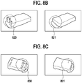
- FIG. 8 illustrates an image of a component generated using depth information with reduced noise by a printed circuit board inspection apparatus according to various embodiments of the present disclosure.
- the printed circuit board inspection apparatus 100 may generate depth information on a component by using a pattern of light reflected from the component among patterns of light irradiated on the component mounted on the printed circuit board, from a plurality of first light sources.
- the printed circuit board inspection apparatus 100 may generate a 3D image of the component by using the generated depth information.
- noise may occur in multiple reflections of light irradiated on the printed circuit board or in the process of processing the received light by the image sensor. If the generated noise is not reduced, the quality of the 3D image of the component generated by the printed circuit board inspection apparatus 100 may be deteriorated, and accurate inspection of the mounting state of the component may not be performed.
- the printed circuit board inspection apparatus 100 may reduce noise from the depth information on the component by using a machine-learning-based model, and may generate the 3D image of the component by using the depth information with reduced noise. Since the 3D image generated using the depth information with reduced noise may more accurately display the shape of the component, more accurate inspection of the mounting state of the component can be performed.
- a shape of a connection portion 810 (e.g., solder paste or the like) between the component and the printed circuit board may be displayed as an abnormal shape in the 3D image or displayed as having a hole, due to the noise.
- a shape of a connection portion 811 (e.g., solder paste or the like) between the component and the printed circuit board may be more accurately displayed in the 3D image.
- a shape of an edge 820 of the component may be displayed as an abnormal shape in the 3D image due to the noise.
- the printed circuit board inspection apparatus 100 reduces noise in the depth information on the component by using the machine-learning-based model and generates the 3D image of the component by using the depth information with reduced noise, a shape of the edge 821 of the component may be more accurately displayed in the 3D image.
- an internal shape 830 of the component may be displayed as an abnormal shape in the 3D image such as having a hole in the component due to the noise.
- an internal shape 831 of the component may be more accurately displayed in the 3D image.
- the printed circuit board inspection apparatus 100 may display the shape of the component more accurately through the 3D image generated using the depth information with reduced noise, thereby performing more accurate inspection of the mounting state of the component.
- the computer-readable recoding medium includes any kind of data storage devices that can be read by a computer system. Examples of the computer-readable recording medium includes ROM, RAM, CD-ROM, magnetic tape, floppy disk, optical data storage device and the like. Also, the computer-readable recoding medium can be distributed to the computer systems which are connected through a network so that the computer-readable codes can be stored and executed in a distribution manner. Further, the functional programs, codes and code segments for implementing the foregoing embodiments can easily be inferred by programmers in the art to which the present disclosure pertains.
Landscapes
- Engineering & Computer Science (AREA)
- Physics & Mathematics (AREA)
- General Physics & Mathematics (AREA)
- Theoretical Computer Science (AREA)
- General Health & Medical Sciences (AREA)
- Health & Medical Sciences (AREA)
- Life Sciences & Earth Sciences (AREA)
- Computer Vision & Pattern Recognition (AREA)
- Software Systems (AREA)
- Artificial Intelligence (AREA)
- Data Mining & Analysis (AREA)
- Evolutionary Computation (AREA)
- Mathematical Physics (AREA)
- General Engineering & Computer Science (AREA)
- Computing Systems (AREA)
- Biophysics (AREA)
- Computational Linguistics (AREA)
- Biomedical Technology (AREA)
- Molecular Biology (AREA)
- Analytical Chemistry (AREA)
- Pathology (AREA)
- Immunology (AREA)
- Biochemistry (AREA)
- Chemical & Material Sciences (AREA)
- Operations Research (AREA)
- Microelectronics & Electronic Packaging (AREA)
- Manufacturing & Machinery (AREA)
- Signal Processing (AREA)
- Optics & Photonics (AREA)
- Multimedia (AREA)
- Quality & Reliability (AREA)
- Length Measuring Devices By Optical Means (AREA)
- Investigating Materials By The Use Of Optical Means Adapted For Particular Applications (AREA)
- Supply And Installment Of Electrical Components (AREA)
- Medical Informatics (AREA)
Applications Claiming Priority (2)
| Application Number | Priority Date | Filing Date | Title |
|---|---|---|---|
| US201862635022P | 2018-02-26 | 2018-02-26 | |
| PCT/KR2019/002330 WO2019164382A1 (fr) | 2018-02-26 | 2019-02-26 | Procédé d'inspection de l'état de montage d'un composant, appareil d'inspection de carte de circuit imprimé et support d'enregistrement lisible par ordinateur |
Publications (4)
| Publication Number | Publication Date |
|---|---|
| EP3761772A1 true EP3761772A1 (fr) | 2021-01-06 |
| EP3761772A4 EP3761772A4 (fr) | 2021-04-28 |
| EP3761772B1 EP3761772B1 (fr) | 2025-07-23 |
| EP3761772C0 EP3761772C0 (fr) | 2025-07-23 |
Family
ID=67687308
Family Applications (2)
| Application Number | Title | Priority Date | Filing Date |
|---|---|---|---|
| EP19756511.2A Active EP3761772B1 (fr) | 2018-02-26 | 2019-02-26 | Procédé d'inspection de l'état de montage d'un composant, appareil d'inspection de carte de circuit imprimé et support d'enregistrement lisible par ordinateur |
| EP19756876.9A Pending EP3761013A4 (fr) | 2018-02-26 | 2019-02-26 | Procédé d'inspection de l'état de montage d'un composant, appareil d'inspection de carte de circuit imprimé et support d'enregistrement lisible par ordinateur |
Family Applications After (1)
| Application Number | Title | Priority Date | Filing Date |
|---|---|---|---|
| EP19756876.9A Pending EP3761013A4 (fr) | 2018-02-26 | 2019-02-26 | Procédé d'inspection de l'état de montage d'un composant, appareil d'inspection de carte de circuit imprimé et support d'enregistrement lisible par ordinateur |
Country Status (5)
| Country | Link |
|---|---|
| US (2) | US11328407B2 (fr) |
| EP (2) | EP3761772B1 (fr) |
| KR (4) | KR102473547B1 (fr) |
| CN (2) | CN111788883B (fr) |
| WO (2) | WO2019164382A1 (fr) |
Families Citing this family (21)
| Publication number | Priority date | Publication date | Assignee | Title |
|---|---|---|---|---|
| US11650164B2 (en) | 2019-05-15 | 2023-05-16 | Getac Technology Corporation | Artificial neural network-based method for selecting surface type of object |
| CN114073175B (zh) * | 2019-07-04 | 2023-09-22 | 株式会社富士 | 元件安装系统 |
| CN111126433A (zh) * | 2019-11-19 | 2020-05-08 | 佛山市南海区广工大数控装备协同创新研究院 | 一种工厂pcb板缺陷检测中正负样本数据平衡方法 |
| US12063745B2 (en) * | 2020-05-05 | 2024-08-13 | Integrated Dynamics Engineering Gmbh | Method for processing substrates, in particular wafers, masks or flat panel displays, with a semi-conductor industry machine |
| KR102459695B1 (ko) | 2020-11-03 | 2022-10-28 | 주식회사 고영테크놀러지 | 실장 정보를 결정하기 위한 장치, 방법 및 명령을 기록한 기록 매체 |
| EP4253943A4 (fr) * | 2020-11-30 | 2024-05-01 | Konica Minolta, Inc. | Dispositif d'analyse, système d'analyse, et dispositif d'apprentissage |
| CN113032919B (zh) | 2021-03-12 | 2022-03-04 | 奥特斯科技(重庆)有限公司 | 部件承载件制造方法、处理系统、计算机程序和系统架构 |
| DE102021114568A1 (de) | 2021-06-07 | 2022-12-08 | Göpel electronic GmbH | Inspektionsvorrichtung zum prüfen von elektronischen bauteilen |
| DE112021008199T5 (de) * | 2021-09-07 | 2024-07-11 | Yamaha Hatsudoki Kabushiki Kaisha | Bauelementmontagesystem |
| CN114018934B (zh) * | 2021-11-03 | 2023-11-03 | 四川启睿克科技有限公司 | 一种用于弧形金属表面缺陷检测的成像系统 |
| KR102455733B1 (ko) * | 2022-02-11 | 2022-10-18 | 주식회사 지오스테크놀러지 | 트랜지스터 아웃라인 패키지 제조 장치 및 이의 제조 방법 |
| KR102770142B1 (ko) * | 2022-02-24 | 2025-02-20 | (주)아이피에스오토 | Ai 비전인식을 이용한 볼트 검사장치 |
| WO2023159298A1 (fr) * | 2022-02-28 | 2023-08-31 | National Research Council Of Canada | Prédiction basée sur l'apprentissage profond de variations structurales induites par un processus de fabrication dans des dispositifs nanophotoniques |
| JP2023177552A (ja) * | 2022-06-02 | 2023-12-14 | キヤノン株式会社 | 記録装置、制御方法、およびプログラム |
| WO2024049199A1 (fr) * | 2022-08-31 | 2024-03-07 | 주식회사 엘지에너지솔루션 | Dispositif et procédé de mesure de dimension basée sur un modèle d'apprentissage |
| CN116448758A (zh) * | 2023-02-10 | 2023-07-18 | 苏州德创测控科技有限公司 | 基于机器视觉的焊点缺陷检测方法、电子设备、存储介质 |
| JP2024135247A (ja) * | 2023-03-22 | 2024-10-04 | 株式会社東芝 | 光学検査方法及びプログラム、並びにそれを用いた光学検査装置 |
| CN116007526B (zh) * | 2023-03-27 | 2023-06-23 | 西安航天动力研究所 | 一种膜片刻痕深度自动测量系统及测量方法 |
| DE102023113821A1 (de) * | 2023-05-25 | 2024-11-28 | ibea Ingenieurbüro für Elektronik und Automatisation GmbH | Inspektionsvorrichtung für Baustoffe und Verfahren zur Inspektion von Baustoffen |
| TWI912687B (zh) * | 2024-01-23 | 2026-01-21 | 撼訊科技股份有限公司 | 顯示卡的自動檢驗方法及系統 |
| KR102801231B1 (ko) * | 2024-08-27 | 2025-04-30 | 주식회사 아이브 | 광을 활용하여 제품의 결함 검사를 수행하는 방법 |
Family Cites Families (35)
| Publication number | Priority date | Publication date | Assignee | Title |
|---|---|---|---|---|
| JPH0989797A (ja) * | 1995-09-25 | 1997-04-04 | Omron Corp | 実装基板検査装置 |
| KR20020046636A (ko) * | 2000-12-15 | 2002-06-21 | 송재인 | 인쇄회로기판의 납땜검사 시스템 및 방법 |
| US7352892B2 (en) * | 2003-03-20 | 2008-04-01 | Micron Technology, Inc. | System and method for shape reconstruction from optical images |
| KR100834113B1 (ko) | 2006-11-10 | 2008-06-02 | 아주하이텍(주) | 자동 광학 검사 시스템 |
| KR101190122B1 (ko) | 2008-10-13 | 2012-10-11 | 주식회사 고영테크놀러지 | 다중파장을 이용한 3차원형상 측정장치 및 측정방법 |
| DE102010029091B4 (de) * | 2009-05-21 | 2015-08-20 | Koh Young Technology Inc. | Formmessgerät und -verfahren |
| US8878929B2 (en) | 2009-05-27 | 2014-11-04 | Koh Young Technology Inc. | Three dimensional shape measurement apparatus and method |
| DE102010030883B4 (de) * | 2009-07-03 | 2018-11-08 | Koh Young Technology Inc. | Vorrichtung zur Prüfung einer Platte und Verfahren dazu |
| DE102010064635B4 (de) | 2009-07-03 | 2024-03-14 | Koh Young Technology Inc. | Verfahren zum Untersuchen eines Messobjektes |
| KR101144749B1 (ko) * | 2010-01-29 | 2012-05-24 | 주식회사 고영테크놀러지 | 소자의 불량 검사방법 |
| KR101078781B1 (ko) | 2010-02-01 | 2011-11-01 | 주식회사 고영테크놀러지 | 3차원 형상 검사방법 |
| US8855403B2 (en) * | 2010-04-16 | 2014-10-07 | Koh Young Technology Inc. | Method of discriminating between an object region and a ground region and method of measuring three dimensional shape by using the same |
| KR101311215B1 (ko) | 2010-11-19 | 2013-09-25 | 경북대학교 산학협력단 | 기판 검사방법 |
| US8755043B2 (en) | 2010-11-19 | 2014-06-17 | Koh Young Technology Inc. | Method of inspecting a substrate |
| KR101684244B1 (ko) * | 2011-03-02 | 2016-12-09 | 주식회사 고영테크놀러지 | 기판 검사방법 |
| US9819879B2 (en) * | 2011-07-12 | 2017-11-14 | Samsung Electronics Co., Ltd. | Image filtering apparatus and method based on noise prediction using infrared ray (IR) intensity |
| US8971612B2 (en) * | 2011-12-15 | 2015-03-03 | Microsoft Corporation | Learning image processing tasks from scene reconstructions |
| KR101215083B1 (ko) * | 2011-12-27 | 2012-12-24 | 경북대학교 산학협력단 | 기판 검사장치의 높이정보 생성 방법 |
| JP5863547B2 (ja) * | 2012-04-20 | 2016-02-16 | ヤマハ発動機株式会社 | プリント基板の検査装置 |
| EP2853855B1 (fr) * | 2012-05-22 | 2016-12-07 | Koh Young Technology Inc. | Procédé de mesure de la hauteur pour un dispositif de mesure de formes tridimensionnelles |
| US20140198185A1 (en) * | 2013-01-17 | 2014-07-17 | Cyberoptics Corporation | Multi-camera sensor for three-dimensional imaging of a circuit board |
| JP2014157086A (ja) | 2013-02-15 | 2014-08-28 | Dainippon Screen Mfg Co Ltd | パターン検査装置 |
| JP2016518747A (ja) * | 2013-03-15 | 2016-06-23 | イェール ユニバーシティーYale University | センサー依存性ノイズを有する画像化データを処理するための技術 |
| KR20150022158A (ko) * | 2013-08-22 | 2015-03-04 | (주)토탈소프트뱅크 | 기계제도 학습장치 및 학습방법 |
| KR20150023205A (ko) * | 2013-08-23 | 2015-03-05 | 주식회사 고영테크놀러지 | 기판 검사방법 및 이를 이용한 기판 검사시스템 |
| JP6296499B2 (ja) * | 2014-08-11 | 2018-03-20 | 株式会社 東京ウエルズ | 透明基板の外観検査装置および外観検査方法 |
| US10533952B2 (en) | 2014-12-08 | 2020-01-14 | Koh Young Technology Inc. | Method of inspecting a terminal of a component mounted on a substrate and substrate inspection apparatus |
| KR101622628B1 (ko) | 2014-12-16 | 2016-05-20 | 주식회사 고영테크놀러지 | 부품이 실장된 기판 검사방법 및 검사장치 |
| US20160321523A1 (en) * | 2015-04-30 | 2016-11-03 | The Regents Of The University Of California | Using machine learning to filter monte carlo noise from images |
| TWI737659B (zh) | 2015-12-22 | 2021-09-01 | 以色列商應用材料以色列公司 | 半導體試樣的基於深度學習之檢查的方法及其系統 |
| CN105891215B (zh) * | 2016-03-31 | 2019-01-29 | 浙江工业大学 | 基于卷积神经网络的焊接视觉检测方法及装置 |
| CN105913427B (zh) * | 2016-04-12 | 2017-05-10 | 福州大学 | 一种基于机器学习的噪声图像显著性检测方法 |
| KR101688458B1 (ko) * | 2016-04-27 | 2016-12-23 | 디아이티 주식회사 | 깊은 신경망 학습 방법을 이용한 제조품용 영상 검사 장치 및 이를 이용한 제조품용 영상 검사 방법 |
| US10346740B2 (en) * | 2016-06-01 | 2019-07-09 | Kla-Tencor Corp. | Systems and methods incorporating a neural network and a forward physical model for semiconductor applications |
| WO2018188466A1 (fr) | 2017-04-12 | 2018-10-18 | Bio-Medical Engineering (HK) Limited | Systèmes et procédés de direction automatisée pour un endoscope robotique |
-
2019
- 2019-02-26 EP EP19756511.2A patent/EP3761772B1/fr active Active
- 2019-02-26 KR KR1020207024788A patent/KR102473547B1/ko active Active
- 2019-02-26 KR KR1020207024783A patent/KR102427381B1/ko active Active
- 2019-02-26 KR KR1020237035082A patent/KR102716521B1/ko active Active
- 2019-02-26 WO PCT/KR2019/002330 patent/WO2019164382A1/fr not_active Ceased
- 2019-02-26 US US16/976,006 patent/US11328407B2/en active Active
- 2019-02-26 CN CN201980015619.0A patent/CN111788883B/zh active Active
- 2019-02-26 US US16/976,008 patent/US11244436B2/en active Active
- 2019-02-26 WO PCT/KR2019/002328 patent/WO2019164381A1/fr not_active Ceased
- 2019-02-26 KR KR1020227041178A patent/KR20220163513A/ko not_active Ceased
- 2019-02-26 CN CN201980015610.XA patent/CN111788476B/zh active Active
- 2019-02-26 EP EP19756876.9A patent/EP3761013A4/fr active Pending
Also Published As
| Publication number | Publication date |
|---|---|
| KR102716521B1 (ko) | 2024-10-16 |
| US20210042910A1 (en) | 2021-02-11 |
| US11244436B2 (en) | 2022-02-08 |
| EP3761013A4 (fr) | 2021-05-12 |
| KR20220163513A (ko) | 2022-12-09 |
| CN111788883B (zh) | 2021-11-05 |
| EP3761772A4 (fr) | 2021-04-28 |
| EP3761772B1 (fr) | 2025-07-23 |
| CN111788476A (zh) | 2020-10-16 |
| CN111788476B (zh) | 2023-07-07 |
| KR20230150886A (ko) | 2023-10-31 |
| KR102473547B1 (ko) | 2022-12-05 |
| KR20200108483A (ko) | 2020-09-18 |
| WO2019164381A1 (fr) | 2019-08-29 |
| WO2019164382A1 (fr) | 2019-08-29 |
| EP3761013A1 (fr) | 2021-01-06 |
| EP3761772C0 (fr) | 2025-07-23 |
| CN111788883A (zh) | 2020-10-16 |
| KR20200108905A (ko) | 2020-09-21 |
| US20210049753A1 (en) | 2021-02-18 |
| US11328407B2 (en) | 2022-05-10 |
| KR102427381B1 (ko) | 2022-08-02 |
Similar Documents
| Publication | Publication Date | Title |
|---|---|---|
| EP3761772B1 (fr) | Procédé d'inspection de l'état de montage d'un composant, appareil d'inspection de carte de circuit imprimé et support d'enregistrement lisible par ordinateur | |
| JP7082715B2 (ja) | 深層畳み込みニューラルネットワークを用いたレーザ加工システムの加工誤差の検出 | |
| CN112505056A (zh) | 缺陷检测方法和装置 | |
| CN113781434B (zh) | 一种缺陷检测方法、装置、智能终端及计算机可读存储介质 | |
| JP6519265B2 (ja) | 画像処理方法 | |
| JP6444233B2 (ja) | 距離計測装置、距離計測方法、およびプログラム | |
| JP2016130663A (ja) | 検査装置及び検査装置の制御方法 | |
| CN113014816A (zh) | 飞拍拍摄触发点的确定方法和装置 | |
| CN113379837B (zh) | 检测设备的角度校正方法、设备及计算机可读存储介质 | |
| US10697765B2 (en) | Image processing apparatus, image processing system, and program therefor | |
| US20110199491A1 (en) | Calibration index determination device, calibration device, calibration performance evaluation device, system, method, and program | |
| US10520424B2 (en) | Adaptive method for a light source for inspecting an article | |
| KR101729862B1 (ko) | 데이터 보정 장치, 묘화 장치, 검사 장치, 데이터 보정 방법, 묘화 방법, 검사 방법 및 기록 매체 | |
| KR101689964B1 (ko) | 데이터 보정 장치, 묘화 장치, 검사 장치, 데이터 보정 방법, 묘화 방법, 검사 방법 및 프로그램을 기록한 기록 매체 | |
| JP2021012043A (ja) | 機械学習用情報処理装置、機械学習用情報処理方法、および機械学習用情報処理プログラム | |
| US20240242330A1 (en) | Image processing apparatus, processing system, image display method, and program | |
| CN113706508A (zh) | 光束质量分析方法、设备、光束分析系统及存储介质 | |
| JP2017026880A (ja) | データ補正装置、描画装置、検査装置、データ補正方法、描画方法、検査方法およびプログラム | |
| KR20220101654A (ko) | 자동화된 육안 검사 스테이션을 위한 오프라인 문제해결 및 개발 | |
| CN119380169B (zh) | 一种视觉检测配置方法、装置及视觉检测系统 | |
| CN116797563A (zh) | 一种基于三维重建的屏幕检测方法、装置及相关介质 | |
| KR20240121072A (ko) | 전자 장치 및 동적 지오메트리 보정 방법 | |
| US20210051303A1 (en) | Information processing apparatus, information processing method, and program | |
| KR20260070926A (ko) | 다중 z축 이동격자패턴 기반 다중카메라 3d 보정 장치 및 방법 | |
| WO2023243430A1 (fr) | Procédé de traitement d'informations, dispositif de traitement d'informations et programme |
Legal Events
| Date | Code | Title | Description |
|---|---|---|---|
| STAA | Information on the status of an ep patent application or granted ep patent |
Free format text: STATUS: THE INTERNATIONAL PUBLICATION HAS BEEN MADE |
|
| PUAI | Public reference made under article 153(3) epc to a published international application that has entered the european phase |
Free format text: ORIGINAL CODE: 0009012 |
|
| STAA | Information on the status of an ep patent application or granted ep patent |
Free format text: STATUS: REQUEST FOR EXAMINATION WAS MADE |
|
| 17P | Request for examination filed |
Effective date: 20200921 |
|
| AK | Designated contracting states |
Kind code of ref document: A1 Designated state(s): AL AT BE BG CH CY CZ DE DK EE ES FI FR GB GR HR HU IE IS IT LI LT LU LV MC MK MT NL NO PL PT RO RS SE SI SK SM TR |
|
| AX | Request for extension of the european patent |
Extension state: BA ME |
|
| REG | Reference to a national code |
Ipc: G06T0005000000 Ref country code: DE Ref legal event code: R079 Ref document number: 602019072918 Country of ref document: DE Free format text: PREVIOUS MAIN CLASS: H05K0013080000 |
|
| A4 | Supplementary search report drawn up and despatched |
Effective date: 20210325 |
|
| RIC1 | Information provided on ipc code assigned before grant |
Ipc: G06T 5/00 20060101AFI20210319BHEP Ipc: G06T 7/521 20170101ALI20210319BHEP Ipc: H05K 13/08 20060101ALI20210319BHEP Ipc: G01N 21/88 20060101ALI20210319BHEP Ipc: G06N 3/04 20060101ALI20210319BHEP Ipc: G01B 11/22 20060101ALI20210319BHEP |
|
| DAV | Request for validation of the european patent (deleted) | ||
| DAX | Request for extension of the european patent (deleted) | ||
| STAA | Information on the status of an ep patent application or granted ep patent |
Free format text: STATUS: EXAMINATION IS IN PROGRESS |
|
| 17Q | First examination report despatched |
Effective date: 20220125 |
|
| REG | Reference to a national code |
Free format text: PREVIOUS MAIN CLASS: G06T0005000000 Ipc: G06T0005600000 Ref country code: DE Ref legal event code: R079 Ref document number: 602019072918 Country of ref document: DE |
|
| GRAP | Despatch of communication of intention to grant a patent |
Free format text: ORIGINAL CODE: EPIDOSNIGR1 |
|
| STAA | Information on the status of an ep patent application or granted ep patent |
Free format text: STATUS: GRANT OF PATENT IS INTENDED |
|
| RIC1 | Information provided on ipc code assigned before grant |
Ipc: G01B 11/22 20060101ALI20240902BHEP Ipc: G06N 3/04 20060101ALI20240902BHEP Ipc: G01N 21/88 20060101ALI20240902BHEP Ipc: H05K 13/08 20060101ALI20240902BHEP Ipc: G06T 7/586 20170101ALI20240902BHEP Ipc: G06T 7/521 20170101ALI20240902BHEP Ipc: G06T 5/70 20240101ALI20240902BHEP Ipc: G06T 5/60 20240101AFI20240902BHEP |
|
| INTG | Intention to grant announced |
Effective date: 20240917 |
|
| GRAJ | Information related to disapproval of communication of intention to grant by the applicant or resumption of examination proceedings by the epo deleted |
Free format text: ORIGINAL CODE: EPIDOSDIGR1 |
|
| STAA | Information on the status of an ep patent application or granted ep patent |
Free format text: STATUS: EXAMINATION IS IN PROGRESS |
|
| INTC | Intention to grant announced (deleted) | ||
| GRAP | Despatch of communication of intention to grant a patent |
Free format text: ORIGINAL CODE: EPIDOSNIGR1 |
|
| STAA | Information on the status of an ep patent application or granted ep patent |
Free format text: STATUS: GRANT OF PATENT IS INTENDED |
|
| INTG | Intention to grant announced |
Effective date: 20250319 |
|
| GRAS | Grant fee paid |
Free format text: ORIGINAL CODE: EPIDOSNIGR3 |
|
| GRAA | (expected) grant |
Free format text: ORIGINAL CODE: 0009210 |
|
| STAA | Information on the status of an ep patent application or granted ep patent |
Free format text: STATUS: THE PATENT HAS BEEN GRANTED |
|
| AK | Designated contracting states |
Kind code of ref document: B1 Designated state(s): AL AT BE BG CH CY CZ DE DK EE ES FI FR GB GR HR HU IE IS IT LI LT LU LV MC MK MT NL NO PL PT RO RS SE SI SK SM TR |
|
| REG | Reference to a national code |
Ref country code: GB Ref legal event code: FG4D |
|
| REG | Reference to a national code |
Ref country code: CH Ref legal event code: EP |
|
| REG | Reference to a national code |
Ref country code: IE Ref legal event code: FG4D |
|
| REG | Reference to a national code |
Ref country code: DE Ref legal event code: R096 Ref document number: 602019072918 Country of ref document: DE |
|
| U01 | Request for unitary effect filed |
Effective date: 20250731 |
|
| U07 | Unitary effect registered |
Designated state(s): AT BE BG DE DK EE FI FR IT LT LU LV MT NL PT RO SE SI Effective date: 20250808 |
|
| PG25 | Lapsed in a contracting state [announced via postgrant information from national office to epo] |
Ref country code: IS Free format text: LAPSE BECAUSE OF FAILURE TO SUBMIT A TRANSLATION OF THE DESCRIPTION OR TO PAY THE FEE WITHIN THE PRESCRIBED TIME-LIMIT Effective date: 20251123 |
|
| PG25 | Lapsed in a contracting state [announced via postgrant information from national office to epo] |
Ref country code: NO Free format text: LAPSE BECAUSE OF FAILURE TO SUBMIT A TRANSLATION OF THE DESCRIPTION OR TO PAY THE FEE WITHIN THE PRESCRIBED TIME-LIMIT Effective date: 20251023 |
|
| PG25 | Lapsed in a contracting state [announced via postgrant information from national office to epo] |
Ref country code: HR Free format text: LAPSE BECAUSE OF FAILURE TO SUBMIT A TRANSLATION OF THE DESCRIPTION OR TO PAY THE FEE WITHIN THE PRESCRIBED TIME-LIMIT Effective date: 20250723 |
|
| PG25 | Lapsed in a contracting state [announced via postgrant information from national office to epo] |
Ref country code: GR Free format text: LAPSE BECAUSE OF FAILURE TO SUBMIT A TRANSLATION OF THE DESCRIPTION OR TO PAY THE FEE WITHIN THE PRESCRIBED TIME-LIMIT Effective date: 20251024 |
|
| PG25 | Lapsed in a contracting state [announced via postgrant information from national office to epo] |
Ref country code: PL Free format text: LAPSE BECAUSE OF FAILURE TO SUBMIT A TRANSLATION OF THE DESCRIPTION OR TO PAY THE FEE WITHIN THE PRESCRIBED TIME-LIMIT Effective date: 20250723 |
|
| PG25 | Lapsed in a contracting state [announced via postgrant information from national office to epo] |
Ref country code: RS Free format text: LAPSE BECAUSE OF FAILURE TO SUBMIT A TRANSLATION OF THE DESCRIPTION OR TO PAY THE FEE WITHIN THE PRESCRIBED TIME-LIMIT Effective date: 20251023 |
|
| PG25 | Lapsed in a contracting state [announced via postgrant information from national office to epo] |
Ref country code: ES Free format text: LAPSE BECAUSE OF FAILURE TO SUBMIT A TRANSLATION OF THE DESCRIPTION OR TO PAY THE FEE WITHIN THE PRESCRIBED TIME-LIMIT Effective date: 20250723 |
|
| U20 | Renewal fee for the european patent with unitary effect paid |
Year of fee payment: 8 Effective date: 20260106 |
|
| PG25 | Lapsed in a contracting state [announced via postgrant information from national office to epo] |
Ref country code: SM Free format text: LAPSE BECAUSE OF FAILURE TO SUBMIT A TRANSLATION OF THE DESCRIPTION OR TO PAY THE FEE WITHIN THE PRESCRIBED TIME-LIMIT Effective date: 20250723 |
|
| PG25 | Lapsed in a contracting state [announced via postgrant information from national office to epo] |
Ref country code: CZ Free format text: LAPSE BECAUSE OF FAILURE TO SUBMIT A TRANSLATION OF THE DESCRIPTION OR TO PAY THE FEE WITHIN THE PRESCRIBED TIME-LIMIT Effective date: 20250723 |
|
| PG25 | Lapsed in a contracting state [announced via postgrant information from national office to epo] |
Ref country code: SK Free format text: LAPSE BECAUSE OF FAILURE TO SUBMIT A TRANSLATION OF THE DESCRIPTION OR TO PAY THE FEE WITHIN THE PRESCRIBED TIME-LIMIT Effective date: 20250723 |