EP3762777B1 - Système de positionnement pour un appareil lithographique - Google Patents
Système de positionnement pour un appareil lithographique Download PDFInfo
- Publication number
- EP3762777B1 EP3762777B1 EP19703749.2A EP19703749A EP3762777B1 EP 3762777 B1 EP3762777 B1 EP 3762777B1 EP 19703749 A EP19703749 A EP 19703749A EP 3762777 B1 EP3762777 B1 EP 3762777B1
- Authority
- EP
- European Patent Office
- Prior art keywords
- coil
- actuator
- magnet
- assembly
- electric conductor
- Prior art date
- Legal status (The legal status is an assumption and is not a legal conclusion. Google has not performed a legal analysis and makes no representation as to the accuracy of the status listed.)
- Active
Links
Images


Classifications
-
- G—PHYSICS
- G03—PHOTOGRAPHY; CINEMATOGRAPHY; ANALOGOUS TECHNIQUES USING WAVES OTHER THAN OPTICAL WAVES; ELECTROGRAPHY; HOLOGRAPHY
- G03F—PHOTOMECHANICAL PRODUCTION OF TEXTURED OR PATTERNED SURFACES, e.g. FOR PRINTING, FOR PROCESSING OF SEMICONDUCTOR DEVICES; MATERIALS THEREFOR; ORIGINALS THEREFOR; APPARATUS SPECIALLY ADAPTED THEREFOR
- G03F7/00—Photomechanical, e.g. photolithographic, production of textured or patterned surfaces, e.g. printing surfaces; Materials therefor, e.g. comprising photoresists; Apparatus specially adapted therefor
- G03F7/70—Microphotolithographic exposure; Apparatus therefor
- G03F7/70691—Handling of masks or workpieces
- G03F7/70758—Drive means, e.g. actuators, motors for long- or short-stroke modules or fine or coarse driving
-
- G—PHYSICS
- G03—PHOTOGRAPHY; CINEMATOGRAPHY; ANALOGOUS TECHNIQUES USING WAVES OTHER THAN OPTICAL WAVES; ELECTROGRAPHY; HOLOGRAPHY
- G03F—PHOTOMECHANICAL PRODUCTION OF TEXTURED OR PATTERNED SURFACES, e.g. FOR PRINTING, FOR PROCESSING OF SEMICONDUCTOR DEVICES; MATERIALS THEREFOR; ORIGINALS THEREFOR; APPARATUS SPECIALLY ADAPTED THEREFOR
- G03F7/00—Photomechanical, e.g. photolithographic, production of textured or patterned surfaces, e.g. printing surfaces; Materials therefor, e.g. comprising photoresists; Apparatus specially adapted therefor
- G03F7/70—Microphotolithographic exposure; Apparatus therefor
- G03F7/70483—Information management; Active and passive control; Testing; Wafer monitoring, e.g. pattern monitoring
-
- G—PHYSICS
- G03—PHOTOGRAPHY; CINEMATOGRAPHY; ANALOGOUS TECHNIQUES USING WAVES OTHER THAN OPTICAL WAVES; ELECTROGRAPHY; HOLOGRAPHY
- G03F—PHOTOMECHANICAL PRODUCTION OF TEXTURED OR PATTERNED SURFACES, e.g. FOR PRINTING, FOR PROCESSING OF SEMICONDUCTOR DEVICES; MATERIALS THEREFOR; ORIGINALS THEREFOR; APPARATUS SPECIALLY ADAPTED THEREFOR
- G03F7/00—Photomechanical, e.g. photolithographic, production of textured or patterned surfaces, e.g. printing surfaces; Materials therefor, e.g. comprising photoresists; Apparatus specially adapted therefor
- G03F7/70—Microphotolithographic exposure; Apparatus therefor
- G03F7/708—Construction of apparatus, e.g. environment aspects, hygiene aspects or materials
- G03F7/70808—Construction details, e.g. housing, load-lock, seals or windows for passing light in or out of apparatus
- G03F7/70825—Mounting of individual elements, e.g. mounts, holders or supports
-
- G—PHYSICS
- G03—PHOTOGRAPHY; CINEMATOGRAPHY; ANALOGOUS TECHNIQUES USING WAVES OTHER THAN OPTICAL WAVES; ELECTROGRAPHY; HOLOGRAPHY
- G03F—PHOTOMECHANICAL PRODUCTION OF TEXTURED OR PATTERNED SURFACES, e.g. FOR PRINTING, FOR PROCESSING OF SEMICONDUCTOR DEVICES; MATERIALS THEREFOR; ORIGINALS THEREFOR; APPARATUS SPECIALLY ADAPTED THEREFOR
- G03F7/00—Photomechanical, e.g. photolithographic, production of textured or patterned surfaces, e.g. printing surfaces; Materials therefor, e.g. comprising photoresists; Apparatus specially adapted therefor
- G03F7/70—Microphotolithographic exposure; Apparatus therefor
- G03F7/708—Construction of apparatus, e.g. environment aspects, hygiene aspects or materials
- G03F7/7095—Materials, e.g. materials for housing, stage or other support having particular properties, e.g. weight, strength, conductivity, thermal expansion coefficient
-
- H—ELECTRICITY
- H02—GENERATION; CONVERSION OR DISTRIBUTION OF ELECTRIC POWER
- H02K—DYNAMO-ELECTRIC MACHINES
- H02K11/00—Structural association of dynamo-electric machines with electric components or with devices for shielding, monitoring or protection
- H02K11/20—Structural association of dynamo-electric machines with electric components or with devices for shielding, monitoring or protection for measuring, monitoring, testing, protecting or switching
- H02K11/21—Devices for sensing speed or position, or actuated thereby
-
- H—ELECTRICITY
- H02—GENERATION; CONVERSION OR DISTRIBUTION OF ELECTRIC POWER
- H02K—DYNAMO-ELECTRIC MACHINES
- H02K41/00—Propulsion systems in which a rigid body is moved along a path due to dynamo-electric interaction between the body and a magnetic field travelling along the path
- H02K41/02—Linear motors; Sectional motors
- H02K41/035—DC motors; Unipolar motors
- H02K41/0352—Unipolar motors
- H02K41/0354—Lorentz force motors, e.g. voice coil motors
- H02K41/0356—Lorentz force motors, e.g. voice coil motors moving along a straight path
-
- G—PHYSICS
- G03—PHOTOGRAPHY; CINEMATOGRAPHY; ANALOGOUS TECHNIQUES USING WAVES OTHER THAN OPTICAL WAVES; ELECTROGRAPHY; HOLOGRAPHY
- G03F—PHOTOMECHANICAL PRODUCTION OF TEXTURED OR PATTERNED SURFACES, e.g. FOR PRINTING, FOR PROCESSING OF SEMICONDUCTOR DEVICES; MATERIALS THEREFOR; ORIGINALS THEREFOR; APPARATUS SPECIALLY ADAPTED THEREFOR
- G03F7/00—Photomechanical, e.g. photolithographic, production of textured or patterned surfaces, e.g. printing surfaces; Materials therefor, e.g. comprising photoresists; Apparatus specially adapted therefor
- G03F7/70—Microphotolithographic exposure; Apparatus therefor
- G03F7/70008—Production of exposure light, i.e. light sources
- G03F7/70033—Production of exposure light, i.e. light sources by plasma extreme ultraviolet [EUV] sources
Definitions
- the present invention relates to a positioning system, a lithographic apparatus comprising such positioning system, a projection system for a lithographic apparatus comprising such a positioning system, a stage apparatus for a lithographic apparatus comprising such a positioning system, an electron beam inspection apparatus comprising such a positioning system, and a method of positioning a structure.
- a lithographic apparatus is a machine that applies a desired pattern onto a substrate, usually onto a target portion of the substrate.
- a lithographic apparatus can be used, for example, in the manufacture of integrated circuits (ICs).
- a patterning device which is alternatively referred to as a mask or a reticle, may be used to generate a circuit pattern to be formed on an individual layer of the IC.
- This pattern can be transferred onto a target portion (e.g. comprising part of, one, or several dies) on a substrate (e.g. a silicon wafer). Transfer of the pattern is typically via imaging onto a layer of radiation-sensitive material (resist) provided on the substrate.
- resist radiation-sensitive material
- a single substrate will contain a network of adjacent target portions that are successively patterned.
- lithographic apparatus include so-called steppers, in which each target portion is irradiated by exposing an entire pattern onto the target portion at one time, and so-called scanners, in which each target portion is irradiated by scanning the pattern through a radiation beam in a given direction (the "scanning"-direction) while synchronously scanning the substrate parallel or anti-parallel to this direction. It is also possible to transfer the pattern from the patterning device to the substrate by imprinting the pattern onto the substrate.
- a lithographic apparatus comprises one or more positioning devices or positioning systems for positioning or displacing components or objects of the apparatus or inside the apparatus.
- Such a positioning system may e.g. comprise an actuator such as an electromagnetic actuator which comprises a coil assembly and a magnet assembly.
- Positioning devices comprising a coil assembly and a magnet assembly are e.g. known from US 2004/239911 , US 2007/205674 and US 4439699 .
- the coil assembly when driven by a drive current, generates a magnetic field, the drive current interacts with a magnetic field provided by the magnet assembly, as may result in a force between the coil assembly and the magnet assembly.
- the magnet assembly and the coil assembly may be movable in respect of each other, allowing one of the magnet assembly and the coil assembly to move, when subjected to the force, in respect of the other one of the magnet assembly and the coil assembly.
- phase lag tends to occur in a motor constant, providing a delay in force as a function of current with increasing frequency.
- a positioning system to position a structure according to claim 1.
- a lithographic apparatus comprising the positioning system according to the invention to position a structure of the lithographic apparatus.
- a stage apparatus for a lithographic apparatus comprising an object table and the positioning system according to the invention for positioning the object table.
- an electron beam inspection apparatus comprising the positioning system according to the invention.
- Figure 1 schematically depicts a lithographic apparatus according to one embodiment of the invention.
- the apparatus comprises an illumination system IL, a support structure MT, a substrate table WT and a projection system PS.
- the illumination system IL is configured to condition a radiation beam B.
- the support structure MT e.g. a mask table
- the substrate table WT e.g. a wafer table
- the projection system PS is configured to project a pattern imparted to the radiation beam B by patterning device MA onto a target portion C (e.g. comprising one or more dies) of the substrate W.
- the illumination system IL may include various types of optical components, such as refractive, reflective, magnetic, electromagnetic, electrostatic or other types of optical components, or any combination thereof, for directing, shaping, or controlling radiation.
- optical components such as refractive, reflective, magnetic, electromagnetic, electrostatic or other types of optical components, or any combination thereof, for directing, shaping, or controlling radiation.
- UV radiation e.g. having a wavelength of or about 365, 355, 248, 193, 157 or 126 nm
- EUV radiation e.g. having a wavelength in the range of 5-20 nm
- particle beams such as ion beams or electron beams.
- the support structure MT supports, i.e. bears the weight of, the patterning device MA.
- the support structure MT holds the patterning device MA in a manner that depends on the orientation of the patterning device MA, the design of the lithographic apparatus, and other conditions, such as for example whether or not the patterning device MA is held in a vacuum environment.
- the support structure MT can use mechanical, vacuum, electrostatic or other clamping techniques to hold the patterning device MA.
- the support structure MT may be a frame or a table, for example, which may be fixed or movable as required.
- the support structure MT may ensure that the patterning device MA is at a desired position, for example with respect to the projection system PS.
- patterning device used herein should be broadly interpreted as referring to any device that can be used to impart a radiation beam B with a pattern in its cross-section such as to create a pattern in a target portion C of the substrate W. It should be noted that the pattern imparted to the radiation beam B may not exactly correspond to the desired pattern in the target portion C of the substrate W, for example if the pattern includes phase-shifting features or so called assist features. Generally, the pattern imparted to the radiation beam will correspond to a particular functional layer in a device being created in the target portion C, such as an integrated circuit.
- the patterning device MA may be transmissive or reflective.
- Examples of patterning devices include masks, programmable mirror arrays, and programmable LCD panels.
- Masks are well known in lithography, and include mask types such as binary, alternating phase-shift, and attenuated phase-shift, as well as various hybrid mask types.
- An example of a programmable mirror array employs a matrix arrangement of small mirrors, each of which can be individually tilted so as to reflect an incoming radiation beam B in different directions. The tilted mirrors impart a pattern in a radiation beam B which is reflected by the mirror matrix.
- projection system used herein should be broadly interpreted as encompassing any type of projection system, including refractive, reflective, catadioptric, magnetic, electromagnetic and electrostatic optical systems, or any combination thereof, as appropriate for the exposure radiation being used, or for other factors such as the use of an immersion liquid or the use of a vacuum.
- the apparatus is of a transmissive type (e.g. employing a transmissive mask).
- the apparatus may be of a reflective type (e.g. employing a programmable mirror array of a type as referred to above, or employing a reflective mask).
- the lithographic apparatus may be of a type having two (dual stage) or more substrate tables WT (and/or two or more mask tables). In such "multiple stage" machines the additional tables may be used in parallel, or preparatory steps may be carried out on one or more tables while one or more other tables are being used for exposure.
- the lithographic apparatus may have a measurement stage that is arranged to be at a position beneath the projection system PS when the substrate table WT is away from that position.
- the measurement stage may be provided with sensors to measure properties of the lithographic apparatus.
- the projection system may project an image on a sensor on the measurement stage to determine an image quality.
- the lithographic apparatus may also be of a type wherein at least a portion of the substrate W may be covered by a liquid having a relatively high refractive index, e.g. water, so as to fill a space between the projection system and the substrate.
- a liquid having a relatively high refractive index e.g. water
- An immersion liquid may also be applied to other spaces in the lithographic apparatus, for example, between the patterning device MA and the projection system PS. Immersion techniques are well known in the art for increasing the numerical aperture of projection systems.
- immersion as used herein does not mean that a structure, such as a substrate W, must be submerged in liquid, but rather only means that liquid is located between the projection system PS and the substrate W during exposure.
- the illumination system IL receives a radiation beam B from a radiation source SO.
- the radiation source SO and the lithographic apparatus may be separate entities, for example when the radiation source SO is an excimer laser. In such cases, the source is not considered to form part of the lithographic apparatus and the radiation beam B is passed from the radiation source SO to the illumination system IL with the aid of a beam delivery system BD comprising, for example, suitable directing mirrors and/or a beam expander.
- the radiation source SO may be an integral part of the lithographic apparatus, for example when the radiation source SO is a mercury lamp.
- the radiation source SO and the illuminator IL, together with the beam delivery system BD if required, may be referred to as a radiation system.
- the illumination system IL may comprise an adjuster AD for adjusting the angular intensity distribution of the radiation beam B.
- an adjuster AD for adjusting the angular intensity distribution of the radiation beam B.
- the illumination system IL may comprise various other components, such as an integrator IN and a condenser CO.
- the illumination system IL may be used to condition the radiation beam B, to have a desired uniformity and intensity distribution in its cross-section.
- the radiation beam B is incident on the patterning device MT, which is held on the support structure MT, and is patterned by the patterning device MA. Having traversed the patterning device MA, the radiation beam B passes through the projection system PS, which focuses the beam onto a target portion C of the substrate W.
- the substrate table WT can be moved accurately, e.g. so as to position different target portions C in the path of the radiation beam B.
- the first positioner PM and another position sensor can be used to accurately position the patterning device MA with respect to the path of the radiation beam B, e.g. after mechanical retrieval from a mask library, or during a scan.
- movement of the support structure MT may be realized with the aid of a long-stroke module and a short-stroke module, which form part of the first positioner PM.
- the long-stroke module may provide coarse positioning of the short-stroke module over a large range of movement.
- the short-stroke module may provide fine positioning of the support structure MT relative to the long-stroke module over a small range of movement.
- movement of the substrate table WT may be realized using a long-stroke module and a short-stroke module, which form part of the second positioner PW.
- the long-stroke module may provide coarse positioning of the short-stroke module over a large range of movement.
- the short-stroke module may provide fine positioning of the substrate table WT relative to the long-stroke module over a small range of movement.
- the support structure MT may be connected to a short-stroke actuator only, or may be fixed.
- Patterning device MA and substrate W may be aligned using mask alignment marks M1, M2 and substrate alignment marks P1, P2.
- the substrate alignment marks P1, P2 as illustrated occupy dedicated target portions, they may be located in spaces between target portions C (these are known as scribe-lane alignment marks). Similarly, in situations in which more than one die is provided on the patterning device MA, the mask alignment marks M1, M2 may be located between the dies.
- the depicted apparatus could be used in at least one of the following modes:
- a first mode the so-called step mode
- the support structure MT and the substrate table WT are kept essentially stationary, while an entire pattern imparted to the radiation beam B is projected onto a target portion C at one time (i.e. a single static exposure).
- the substrate table WT is then shifted in the X and/or Y direction so that a different target portion C can be exposed.
- the maximum size of the exposure field limits the size of the target portion C imaged in a single static exposure.
- a second mode the so-called scan mode
- the support structure MT and the substrate table WT are scanned synchronously while a pattern imparted to the radiation beam B is projected onto a target portion C (i.e. a single dynamic exposure).
- the velocity and direction of the substrate table WT relative to the support structure MT may be determined by the (de-)magnification and image reversal characteristics of the projection system PS.
- scan mode the maximum size of the exposure field limits the width (in the non-scanning direction) of the target portion in a single dynamic exposure, whereas the length of the scanning motion determines the height (in the scanning direction) of the target portion.
- the support structure MT is kept essentially stationary holding a programmable patterning device, and the substrate table WT is moved or scanned while a pattern imparted to the radiation beam B is projected onto a target portion C.
- a pulsed radiation source is employed and the programmable patterning device is updated as required after each movement of the substrate table WT or in between successive radiation pulses during a scan.
- This mode of operation can be readily applied to maskless lithography that utilizes programmable patterning device, such as a programmable mirror array of a type as referred to above.
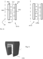
- Figure 2A depicts a cross sectional view of a part of an actuator ACT according to the prior art, the cross sectional view along the lines A-A of the top view of the actuator as depicted in Figure 2B .
- the actuator comprises a coil assembly CA and a magnet assembly MA.
- the coil assembly and magnet assembly are movable in respect of each other.
- the coil assembly may be movable, the magnet assembly may be movable, or both the coil assembly and the magnet assembly may be movable.
- a positioning system POS for positioning a structure STR comprises the actuator ACT and a control unit CU.
- the structure may be any object.
- the control unit comprises a setpoint input for receiving a setpoint SET, i.e.
- the control unit drives the actuator based on the setpoint.
- an amplifier AMP may be provided that drives the actuator, i.e. drives the coil of the coil assembly, in response to an output signal provided by the control unit and input to the amplifier.
- the positioning system may further comprise a position sensing system PMS to measure a position of the structure and comprising one or more position sensors (interferometers, encoders, capacitive sensors or any other suitable position sensors), a position signal representing the position of the structure being provided by the position sensing system to the control unit in order to provide a feedback control loop.
- the magnet assembly comprises a magnet MG, such as a permanent magnet. Alternatively, an electromagnet could be applied. Furthermore, the magnet assembly may comprise a back-iron BA. The back-iron conducts a magnetic flux as provided by the magnet towards the coil assembly so as to concentrate a magnetic flux at the coil assembly.
- the back-iron may comprise iron or any other suitable (ferromagnetic) material capable of conducting magnetic flux.
- the coil assembly comprises windings forming an electric coil CL provided in a coil housing CH.
- the coil housing may hold the coil, provide a packaging of windings of the coil, may comprise a metal (e.g. a non-ferromagnetic conductor) and may provide for heat sinking to conduct dissipated heat away from the coil windings.
- the actuator may position any structure, i.e. any object.
- the structure may be connected to one of the magnet assemble and the coil assembly.
- the other one of the magnet assembly and the coil assembly may for example be connected to a reference frame, force frame, base frame, balance mass or other reference structure.
- the positioning system comprising the actuator ACT as depicted in Figure 2A may be circular symmetric.
- the cross sectional view as depicted in Figure 2A may circularly repeat to form a ring shaped actuator as depicted in Figure 2B .
- the coil, of which in Figure 2A a part is shown may be ring shaped (annular).
- the magnet and the back-iron(s) may be ring shaped.
- the back-iron depicted at the left side in Figure 2A may form an inner, annular back-iron and the back-iron depicted at the right side in Figure 2A may form an outer, annular back-iron.
- windings of the coil of the coil assembly may extend annularly.
- Figure 7A depicts a bode diagram of an impedance response of the actuator in accordance with Figure 2A .
- the impedance of the coil is generally resistive as a result of a resistance of the coil windings.
- the impedance increases due to the inductive properties of the coil.
- the phase of the impedance follows a similar behavior.
- Figure 7B depicts a bode diagram of a motor constant of the actuator in accordance with Figure 2A .
- the motor constant is understood as an actuator force as a function of the coil drive current. At low frequency, the motor constant is substantially independent of frequency. At higher frequencies, the motor constant decreases. As also shown in Figure 7B , the phase of the motor constant follows a similar behavior. The roll off in the motor constant provides for a delay in the response of the actuator, i.e. a delay in force as a function of drive current.
- Figure 4A depicts a cut out view of a part of an actuator as may be employed in a positioning system.
- the actuator comprises a coil assembly and a magnet assembly generally as described above in relation to the actuator of Figure 2A . Accordingly, reference is made to Figure 2A and the corresponding description for the constituent parts and functions thereof. A general setup of a remainder of the positioning system as described with reference to Figure 3 .
- the magnet assembly of the actuator further comprises a further electric conductor CON.
- the further electric conductor comprises a non-ferromagnetic electric conductor, preferably the further electric conductor being a non-ferromagnetic electric conductor, such as copper or aluminum.
- the further electric conductor is magnetically coupled to the coil of the coil assembly.
- an actuator current flowing in the coil of the coil assembly will induce, by the magnetic coupling, an inductive current in the further electric conductor.
- the current in the coil of the coil assembly will generate a coil magnetic field.
- a current will be induced in the further electric conductor.
- the further electric conductor provides for a short circuit path (e.g. a low electrical resistance path).
- the induced current is short circuited by the short circuit path.
- short circuit path is to be understood as a low resistance closed electrically conductive path.
- the further electric conductor comprises a ferromagnetic material
- magnetic permeability will substantially be unaltered by the presence of the further electric conductor hence, the magnetic field by the actuator current in the coil will be substantially unaltered by the presence of the further electric conductor.
- the further electric conductor may exhibit an electric conductivity that exceeds an electric conductivity of the magnet and/or the back iron to provide a low resistance, hence to effectively reduce the coil impedance as explained below.
- the coil when driven by a drive current, generates a coil magnetic field.
- inductive currents will be induced in the further electric conductor.
- the inductive currents will, to some extent, provide for a, generally weaker, counter magnetic field that opposes the coil magnetic field to some extent.
- the coil magnetic field will be kept intact up to higher frequencies, providing for a reduction of the impedance of the actuator at higher frequencies. Illustrated in a different way: due to the magnetic coupling between the further electric conductor and the coil, and the low impedance electrical path in the further electric conductor, at higher frequencies, an effective impedance of the coil is reduced, in a similar way as a short circuited secondary winding of a transformer (compare: the low impedance path in the further electric conductor) would reduce an impedance of the primary winding of the transformer (compare the impedance of coil in the coil assembly). A dynamic performance of the positioning system may be improved and high frequency amplifier dissipation may be reduced. Furthermore, delay reduction may be provided as explained in more detail further below.
- the further electric conductor may have any suitable shape.
- the further electric conductor faces the coil assembly, i.e. is provided on a surface of the magnet and/or the back-iron which surface faces the coil assembly, so as to have the inductive currents at relative short distance of the coil assembly.
- the short circuit path formed by the further electric conductor may be coaxial with the windings of the coil, thus providing a good magnetic coupling hence an effective reduction in impedance at higher frequencies.
- the actuator may be ring shaped.
- the further electric conductor as depicted in Figures 4A and 4B may be ring shaped.
- the further electric conductor will form a closed winding that is able to short circuit the inductive currents, thus providing for a low resistance conductive path for the inductive currents.
- a relatively thin layer of the further electric conductor between the coil assembly and the magnet respectively the back-iron may be sufficient to provide a low resistance conductive path.
- the relatively thin layer of further electric conductor allows a gap between the coil assembly and the magnet assembly to remain small, thus avoiding to sacrifice actuator performance (e.g. motor steepness) to a large extent.
- the ring shape of the further electric conductor may be co-axial with the ring shape of the magnet assembly and the ring shape of the coil assembly.
- the low resistance conductive path of the ring shape of the further electric conductor may be combined with the ring shape of the coil assembly and magnet assembly to provide a uniform effect by the inductive currents along a circumference of the magnet assembly and the coil assembly.
- Figure 4C depicts a cut out view of a part of another actuator ACT2 as may be employed in a positioning system. Similar to the actuator ACT as described above, the actuator ACT2 is a rotational symmetrical actuator, symmetrically about the axis SA.
- the actuator ACT2 comprises a coil assembly CA2 and a magnet assembly MA2.
- the magnet assembly MA2 comprises a back-iron BA2 onto which three cylindrical magnets MG2 are mounted, the magnets MG2 having a magnetization direction as indicated by the arrows.
- the coil assembly CA2 comprises two coils CL2 mounted to a back-iron BC2.
- the actuator ACT2 may also be provided with a further electrical conductor CON2 having the same or similar functionality as the further electrical conductor CON described above.
- Figure 5 depicts a detailed view of a part of the magnet and back iron of the actuator in accordance with Figure 4B .
- Figure 5 likewise depicts the further conductor.
- the inductive currents as induced in the further conductor are schematically indicated by the lines on the further conductor, the lines extending annularly to represent the ring shaped short circuited inductive currents.
- the further electric conductor may form a layer on the magnet, the back-iron or both.
- a thickness of the further electric conductor may be in a range of e.g. micrometers to millimeters.
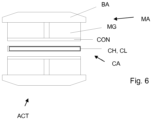
- Such a flat actuator may for example comprise a linear motor such as a short stroke motor of a stage, e.g. an actuator which exerts a force in a direction along a plane parallel to a gap between the coil assembly and the magnet assembly.
- a linear motor such as a short stroke motor of a stage
- an actuator which exerts a force in a direction along a plane parallel to a gap between the coil assembly and the magnet assembly.
- An example is depicted in Figure 6 .
- the further electric conductor CON may be arranged on the magnet assembly MA, for example the further electric conductor may form a conductive plate, such as a copper plate on the magnet assembly.
- the actuator may provide for a force and positioning in a direction parallel to the plate (or perpendicular to the plate).
- Figure 8A depicts a bode diagram of an impedance response of the actuator in accordance with Figure 4A resp. 4B. Also, for comparison, the curves of Figure 7A are copied into Figure 8A . Comparing a magnitude of the impedance response of the actuator according to Fig. 4A and 4B with the actuator according to Figure 2A , an impedance at higher frequencies is lower. As also shown in Figure 8A , the phase change of the impedance at higher frequencies is less in the embodiment in accordance with Figure 4A and 4B as compared to the actuator in accordance with Figure 2A . Thus, as the inductive currents keep the coil field intact at higher frequencies, the impedance of the actuator is reduced. Hence the control unit and the amplifier may drive the actuator at higher frequencies, thus enabling to increase a bandwidth of the positioning system.
- Figure 8B depicts a bode diagram of a motor constant of the actuator in accordance with Figure 4A resp. 4B.
- the motor constant is understood as an actuator force as a result of the coil drive current.
- the curves of Figure 7B are copied into Figure 8B .
- the high frequency roll off of the motor constant is less in the embodiments in accordance with Figures 4A and 4B as compared to the actuator of Figure 2A .
- the phase of the motor constant follows a corresponding behavior.
- the further electric conductor provides for less high frequency roll-off in the motor constant, and less high frequency phase change of the motor constant.
- the coil assembly may further comprise a coil housing in which the coil is arranged.
- the coil housing may comprise a metal, thereby on the one hand mechanically protecting the windings of the coil and on the other hand guiding heat away from the windings.
- inductive currents may be generated in the coil housing also.
- the inductive currents in the coil housing are reduced.
- the delay in the motor constant may be reduced. Therefore, a delay of the feedback loop of the positioning system may be reduced, providing a faster response of the positioning system to dynamics in the setpoint.
- the positioning system comprising the actuator having the further electric conductor may be applied in a lithographic apparatus, i.e. may form a positioning system in a lithographic apparatus.
- the positions system according to the invention may be comprised in a stage apparatus for a lithographic apparatus.
- the actuator having the further electric conductor may for example form a short stroke actuator or vertical actuator of the stage, hence enabling a fast positioning by the enhanced bandwidth capabilities as explained above.
- the stage may comprise a substrate stage (wafer table) or a mask stage (patterning device).
- the actuator comprising the further electric conductor may form an actuator of an optical element of the projection system.
- the optical element may for example be a mirror of a projection optical box in a reflective projection system for Extreme Ultra Violet radiation, or a lens in a transmissive projection system, hence enabling a fast positioning of the optical element, as may for example be applied when driving the optical element position to e.g. adapt according to a substrate height map.
- the invention may further encompass a method of positioning a structure, by a positioning system,
- lithographic apparatus in the manufacture of ICs
- the lithographic apparatus described herein may have other applications, such as the manufacture of integrated optical systems, guidance and detection patterns for magnetic domain memories, flat-panel displays, liquid-crystal displays (LCDs), thin-film magnetic heads, etc.
- LCDs liquid-crystal displays
- any use of the terms “wafer” or “die” herein may be considered as synonymous with the more general terms “substrate” or "target portion”, respectively.
- the substrate referred to herein may be processed, before or after exposure, in for example a track (a tool that typically applies a layer of resist to a substrate and develops the exposed resist), a metrology tool and/or an inspection tool. Where applicable, the disclosure herein may be applied to such and other substrate processing tools. Further, the substrate may be processed more than once, for example in order to create a multi-layer IC, so that the term substrate used herein may also refer to a substrate that already contains multiple processed layers.
- imprint lithography a topography in a patterning device defines the pattern created on a substrate.
- the topography of the patterning device may be pressed into a layer of resist supplied to the substrate whereupon the resist is cured by applying electromagnetic radiation, heat, pressure or a combination thereof.
- the patterning device is moved out of the resist leaving a pattern in it after the resist is cured.
- the invention may take the form of a computer program containing one or more sequences of machine-readable instructions describing a method as disclosed above, or a data storage medium (e.g. semiconductor memory, magnetic or optical disk) having such a computer program stored therein.
- a data storage medium e.g. semiconductor memory, magnetic or optical disk
Landscapes
- Engineering & Computer Science (AREA)
- Physics & Mathematics (AREA)
- General Physics & Mathematics (AREA)
- Power Engineering (AREA)
- Environmental & Geological Engineering (AREA)
- Electromagnetism (AREA)
- Combustion & Propulsion (AREA)
- Health & Medical Sciences (AREA)
- Chemical & Material Sciences (AREA)
- Epidemiology (AREA)
- Public Health (AREA)
- Microelectronics & Electronic Packaging (AREA)
- Exposure And Positioning Against Photoresist Photosensitive Materials (AREA)
- Container, Conveyance, Adherence, Positioning, Of Wafer (AREA)
- Reciprocating, Oscillating Or Vibrating Motors (AREA)
- Linear Motors (AREA)
- Exposure Of Semiconductors, Excluding Electron Or Ion Beam Exposure (AREA)
Claims (10)
- Un système de positionnement (POS) pour positionner une structure (STR), le système de positionnement (POS) comprenant un actionneur (ACT) et une unité de commande (CU) pour commander l'actionneur (ACT) en réponse à un point de consigne de position reçu par l'unité de commande (CU), l'actionneur (ACT) comprenant :un ensemble à aimant (MA) qui comprend un aimant (MG) configuré pour fournir un flux magnétique, et un ensemble à bobine (CA), où l'ensemble à bobine (CA) et l'ensemble à aimant (MA) sont déplaçables l'un relativement à l'autre, l'ensemble à bobine (CA) comprenant une bobine (CL), un actionnement de la bobine (CL) par un courant d'excitation fournissant une force entre l'ensemble à aimant (MA) et l'ensemble à bobine (CA),où l'ensemble à aimant (MA) comprend un conducteur électrique supplémentaire (CON), le conducteur électrique supplémentaire (CON) comprenant un matériau électroconducteur non ferromagnétique, où le conducteur électrique supplémentaire (CON) est couplé magnétiquement à la bobine (CL) de l'ensemble à bobine (CA) et forme un chemin de court-circuit pour un courant électrique inductif induit dans le conducteur électrique supplémentaire (CON) en conséquence d'un courant d'actionneur dans la bobine (CL), caractérisé en ce que l'actionneur (ACT) forme un actionneur linéaire plat, configuré pour exercer une force dans une direction suivant un plan parallèle à un entrefer entre l'ensemble à bobine (CA) et l'ensemble à aimant (MA), le conducteur électrique supplémentaire (CON) formant une plaque conductrice sur l'ensemble à aimant (MA) s'étendant suivant le plan.
- Le système de positionnement (POS) selon la revendication 1, où l'ensemble à aimant (MA) comprend un premier ensemble à aimant substantiellement plat comprenant un premier contrefer et un premier aimant, et un deuxième ensemble à aimant substantiellement plat comprenant un deuxième contrefer et un deuxième aimant, où le premier aimant fait face au deuxième aimant, où l'ensemble à bobine (CA) est agencé dans un entrefer entre le premier ensemble à aimant et le deuxième ensemble à aimant, et où le conducteur électrique supplémentaire (CON) comprend une première plaque conductrice montée sur le premier aimant et une deuxième plaque conductrice montée sur le deuxième aimant.
- Le système de positionnement (POS) selon la revendication 1 ou la revendication 2, où une conductivité électrique du conducteur électrique supplémentaire (CON) dépasse une conductivité électrique de l'aimant (MG).
- Le système de positionnement (POS) selon n'importe lesquelles des revendications précédentes, où le chemin de court-circuit formé par le conducteur électrique supplémentaire (CON) est coaxial avec des spires de la bobine (CL).
- Le système de positionnement (POS) selon n'importe lesquelles des revendications précédentes, où l'actionneur (ACT) comprend un stator et une pièce mobile qui est déplaçable par rapport au stator, le stator comprenant l'ensemble à aimant (MA) et la pièce mobile comprenant l'ensemble à bobine (CA).
- Le système de positionnement (POS) selon n'importe lesquelles des revendications précédentes, comprenant en sus un système de mesure de position pour mesurer une position de la structure, et un amplificateur raccordé à l'actionneur (ACT) pour exciter la bobine (CL), où l'unité de commande (CU) comprend une entrée captant la position, la position telle que mesurée par le système de mesure de position étant fournie à l'entrée captant la position, et où l'unité de commande (CU) comprend une sortie raccordée à une entrée de l'amplificateur, l'unité de commande (CU) étant configurée pour exciter l'amplificateur sur la base du point de consigne de position et de la position telle que mesurée par le système de mesure de position.
- Un appareil lithographique comprenant le système de positionnement selon n'importe lesquelles des revendications précédentes pour positionner une structure de l'appareil lithographique.
- Un appareil à platine pour un appareil lithographique, l'appareil à platine comprenant une table porte-objet et le système de positionnement selon n'importe lesquelles des revendications 1 à 6 pour positionner la table porte-objet.
- Un appareil d'inspection à faisceau d'électrons comprenant le système de positionnement selon n'importe lesquelles des revendications 1 à 6.
- Un procédé de positionnement d'une structure par un système de positionnement,
le système de positionnement comprenant un actionneur et une unité de commande pour commander l'actionneur en réponse à un point de consigne de position reçu par l'unité de commande, l'actionneur comprenant :un ensemble à aimant qui comprend un aimant configuré pour fournir un flux magnétique, et un ensemble à bobine, où l'ensemble à bobine et l'ensemble à aimant sont déplaçables l'un relativement à l'autre, l'ensemble à bobine comprenant une bobine, un actionnement de la bobine par un courant d'excitation fournissant une force entre l'ensemble à aimant et l'ensemble à bobine,où l'ensemble à aimant comprend un conducteur électrique supplémentaire, le conducteur électrique supplémentaire comprenant un matériau électroconducteur non ferromagnétique, où le conducteur électrique supplémentaire est couplé magnétiquement à la bobine de l'ensemble à bobine et forme un chemin de court-circuit pour un courant électrique inductif induit dans le conducteur électrique supplémentaire en conséquence d'un courant d'actionneur dans la bobine,l'actionneur forme un actionneur linéaire plat, configuré pour exercer une force dans une direction suivant un plan parallèle à un entrefer entre l'ensemble à bobine et l'ensemble à aimant, le conducteur électrique supplémentaire formant une plaque conductrice sur l'ensemble à aimant s'étendant suivant le plan, le procédé comprenant :
l'excitation, au moyen de l'unité de commande, d'un courant d'actionneur dans l'ensemble à bobine, induisant de ce fait le courant inductif dans le conducteur électrique supplémentaire, le courant inductif étant court-circuité par le chemin de court-circuit.
Applications Claiming Priority (2)
| Application Number | Priority Date | Filing Date | Title |
|---|---|---|---|
| EP18160934 | 2018-03-09 | ||
| PCT/EP2019/053613 WO2019170379A1 (fr) | 2018-03-09 | 2019-02-14 | Système de positionnement pour un appareil lithographique |
Publications (2)
| Publication Number | Publication Date |
|---|---|
| EP3762777A1 EP3762777A1 (fr) | 2021-01-13 |
| EP3762777B1 true EP3762777B1 (fr) | 2023-11-08 |
Family
ID=61616932
Family Applications (1)
| Application Number | Title | Priority Date | Filing Date |
|---|---|---|---|
| EP19703749.2A Active EP3762777B1 (fr) | 2018-03-09 | 2019-02-14 | Système de positionnement pour un appareil lithographique |
Country Status (7)
| Country | Link |
|---|---|
| US (1) | US11156925B2 (fr) |
| EP (1) | EP3762777B1 (fr) |
| JP (1) | JP7051261B2 (fr) |
| CN (1) | CN111868631A (fr) |
| NL (1) | NL2022570A (fr) |
| TW (1) | TWI688839B (fr) |
| WO (1) | WO2019170379A1 (fr) |
Families Citing this family (2)
| Publication number | Priority date | Publication date | Assignee | Title |
|---|---|---|---|---|
| US12360058B2 (en) * | 2020-12-21 | 2025-07-15 | Kla Corporation | Integration of an optical height sensor in mask inspection tools |
| DE102024204660A1 (de) * | 2024-05-21 | 2025-11-27 | Carl Zeiss Smt Gmbh | Optische Baugruppe, Verfahren zur Integration der optischen Baugruppe und Projektionsbelichtungsanlage |
Citations (4)
| Publication number | Priority date | Publication date | Assignee | Title |
|---|---|---|---|---|
| US4439699A (en) * | 1982-01-18 | 1984-03-27 | International Business Machines Corporation | Linear moving coil actuator |
| US20010023927A1 (en) * | 1998-08-14 | 2001-09-27 | Hazelton Andrew J. | Reaction force isolation system for a planar motor |
| US20050099069A1 (en) * | 2003-11-06 | 2005-05-12 | Koorneef Lucas F. | Hermetically sealed elements of an actuator |
| EP1882983A1 (fr) * | 2006-07-25 | 2008-01-30 | Carl Zeiss SMT AG | Support de compensation de la gravité pour élément optique |
Family Cites Families (21)
| Publication number | Priority date | Publication date | Assignee | Title |
|---|---|---|---|---|
| US4717874A (en) * | 1984-02-10 | 1988-01-05 | Kabushiki Kaisha Sg | Reluctance type linear position detection device |
| JPS63242160A (ja) | 1987-03-27 | 1988-10-07 | Yaskawa Electric Mfg Co Ltd | リニア同期電動機 |
| US5420468A (en) * | 1990-12-27 | 1995-05-30 | Eastman Kodak Company | Shorted turn for moving coil motors |
| JPH0723554A (ja) | 1993-06-15 | 1995-01-24 | Hitachi Ltd | 直線型アクチュエータ |
| AU2852899A (en) * | 1998-03-19 | 1999-10-11 | Nikon Corporation | Flat motor, stage, exposure apparatus and method of producing the same, and device and method for manufacturing the same |
| JP3540311B2 (ja) * | 2002-05-31 | 2004-07-07 | 松下電器産業株式会社 | モータ駆動制御装置 |
| US6822368B2 (en) | 2002-06-04 | 2004-11-23 | Wavecrest Laboratories, Llc | Rotary permanent magnet electric motor having stator pole shoes of varying dimensions |
| JP4008314B2 (ja) | 2002-08-30 | 2007-11-14 | 三菱重工業株式会社 | 高速誘導電動機 |
| US6906789B2 (en) | 2003-06-02 | 2005-06-14 | Asml Holding N.V. | Magnetically levitated and driven reticle-masking blade stage mechanism having six degrees freedom of motion |
| US7279812B2 (en) * | 2005-01-18 | 2007-10-09 | Hewlett-Packard Development Company, L.P. | Light direction assembly shorted turn |
| US7456935B2 (en) | 2005-04-05 | 2008-11-25 | Asml Netherlands B.V. | Lithographic apparatus and device manufacturing method utilizing a positioning device for positioning an object table |
| TW200709536A (en) * | 2006-03-02 | 2007-03-01 | Magtronics Technology Inc | A voice coil motor and method of using magnetic restoring force achieving displacement control |
| CN101657956B (zh) | 2007-06-13 | 2013-01-16 | 株式会社安川电机 | 密封直线电动机电枢以及密封直线电动机 |
| JP5019451B2 (ja) | 2007-11-15 | 2012-09-05 | 東芝産業機器製造株式会社 | 回転子 |
| EP2073352B1 (fr) | 2007-12-17 | 2016-03-16 | Siemens Aktiengesellschaft | Machine synchrone à excitation permanente dotée d'aimants à coque |
| CN102265219B (zh) * | 2008-12-11 | 2014-07-16 | 卡尔蔡司Smt有限责任公司 | 投射曝光设备中的光学元件的重力补偿 |
| JP6192305B2 (ja) | 2013-02-05 | 2017-09-06 | 株式会社サンエス | 永久磁石型電磁駆動装置 |
| EP2916032B1 (fr) * | 2014-03-05 | 2019-08-14 | Goodrich Actuation Systems SAS | Ensembles d'amortissement débrayable pour des surfaces aérodynamiques mobiles |
| WO2017024409A1 (fr) | 2015-08-11 | 2017-02-16 | Genesis Robotics Llp | Machine électrique |
| US10158313B2 (en) * | 2015-10-15 | 2018-12-18 | Nikon Corporation | Current controller for cryogenically cooled motor |
| JP6659951B2 (ja) * | 2016-03-31 | 2020-03-04 | ミツミ電機株式会社 | アクチュエータ及び電動理美容器具 |
-
2019
- 2019-02-14 WO PCT/EP2019/053613 patent/WO2019170379A1/fr not_active Ceased
- 2019-02-14 JP JP2020542312A patent/JP7051261B2/ja active Active
- 2019-02-14 NL NL2022570A patent/NL2022570A/nl unknown
- 2019-02-14 US US16/976,326 patent/US11156925B2/en active Active
- 2019-02-14 EP EP19703749.2A patent/EP3762777B1/fr active Active
- 2019-02-14 CN CN201980017703.6A patent/CN111868631A/zh active Pending
- 2019-03-05 TW TW108107198A patent/TWI688839B/zh active
Patent Citations (4)
| Publication number | Priority date | Publication date | Assignee | Title |
|---|---|---|---|---|
| US4439699A (en) * | 1982-01-18 | 1984-03-27 | International Business Machines Corporation | Linear moving coil actuator |
| US20010023927A1 (en) * | 1998-08-14 | 2001-09-27 | Hazelton Andrew J. | Reaction force isolation system for a planar motor |
| US20050099069A1 (en) * | 2003-11-06 | 2005-05-12 | Koorneef Lucas F. | Hermetically sealed elements of an actuator |
| EP1882983A1 (fr) * | 2006-07-25 | 2008-01-30 | Carl Zeiss SMT AG | Support de compensation de la gravité pour élément optique |
Also Published As
| Publication number | Publication date |
|---|---|
| US11156925B2 (en) | 2021-10-26 |
| WO2019170379A1 (fr) | 2019-09-12 |
| JP2021516357A (ja) | 2021-07-01 |
| US20210041793A1 (en) | 2021-02-11 |
| JP7051261B2 (ja) | 2022-04-11 |
| EP3762777A1 (fr) | 2021-01-13 |
| TWI688839B (zh) | 2020-03-21 |
| NL2022570A (en) | 2019-09-12 |
| CN111868631A (zh) | 2020-10-30 |
| TW201945868A (zh) | 2019-12-01 |
Similar Documents
| Publication | Publication Date | Title |
|---|---|---|
| US8687171B2 (en) | Electromagnetic actuator, stage apparatus and lithographic apparatus | |
| KR101325619B1 (ko) | 가변 릴럭턴스 디바이스, 스테이지 장치, 리소그래피 장치 및 디바이스 제조방법 | |
| JP5192064B2 (ja) | 変位デバイス、リソグラフィ装置および位置決め方法 | |
| US8373848B2 (en) | Lithographic apparatus and lorentz actuator | |
| US7348752B1 (en) | Stage apparatus and lithographic apparatus | |
| JP5635847B2 (ja) | アクチュエータ、位置決めシステム、およびリソグラフィ装置 | |
| US9811005B2 (en) | Lithographic apparatus and device manufacturing method | |
| US7259832B2 (en) | Lithographic apparatus and device manufacturing method | |
| US7459808B2 (en) | Lithographic apparatus and motor | |
| EP3762777B1 (fr) | Système de positionnement pour un appareil lithographique | |
| US7696652B2 (en) | Electromagnetic actuator, method of manufacturing a part of an electromagnetic actuator, and lithographic apparatus comprising and electromagnetic actuator | |
| US10955759B2 (en) | Lithographic apparatus and device manufacturing method | |
| US20190074756A1 (en) | Magnet array, electric coil device, displacement system, lithographic apparatus and device manufacturing method | |
| NL2012966A (en) | Stage apparatus, lithographic apparatus and device manufacturing method. |
Legal Events
| Date | Code | Title | Description |
|---|---|---|---|
| STAA | Information on the status of an ep patent application or granted ep patent |
Free format text: STATUS: UNKNOWN |
|
| STAA | Information on the status of an ep patent application or granted ep patent |
Free format text: STATUS: THE INTERNATIONAL PUBLICATION HAS BEEN MADE |
|
| PUAI | Public reference made under article 153(3) epc to a published international application that has entered the european phase |
Free format text: ORIGINAL CODE: 0009012 |
|
| STAA | Information on the status of an ep patent application or granted ep patent |
Free format text: STATUS: REQUEST FOR EXAMINATION WAS MADE |
|
| 17P | Request for examination filed |
Effective date: 20200730 |
|
| AK | Designated contracting states |
Kind code of ref document: A1 Designated state(s): AL AT BE BG CH CY CZ DE DK EE ES FI FR GB GR HR HU IE IS IT LI LT LU LV MC MK MT NL NO PL PT RO RS SE SI SK SM TR |
|
| AX | Request for extension of the european patent |
Extension state: BA ME |
|
| DAV | Request for validation of the european patent (deleted) | ||
| DAX | Request for extension of the european patent (deleted) | ||
| STAA | Information on the status of an ep patent application or granted ep patent |
Free format text: STATUS: EXAMINATION IS IN PROGRESS |
|
| 17Q | First examination report despatched |
Effective date: 20211112 |
|
| P01 | Opt-out of the competence of the unified patent court (upc) registered |
Effective date: 20230414 |
|
| GRAP | Despatch of communication of intention to grant a patent |
Free format text: ORIGINAL CODE: EPIDOSNIGR1 |
|
| STAA | Information on the status of an ep patent application or granted ep patent |
Free format text: STATUS: GRANT OF PATENT IS INTENDED |
|
| INTG | Intention to grant announced |
Effective date: 20230703 |
|
| GRAS | Grant fee paid |
Free format text: ORIGINAL CODE: EPIDOSNIGR3 |
|
| GRAA | (expected) grant |
Free format text: ORIGINAL CODE: 0009210 |
|
| STAA | Information on the status of an ep patent application or granted ep patent |
Free format text: STATUS: THE PATENT HAS BEEN GRANTED |
|
| AK | Designated contracting states |
Kind code of ref document: B1 Designated state(s): AL AT BE BG CH CY CZ DE DK EE ES FI FR GB GR HR HU IE IS IT LI LT LU LV MC MK MT NL NO PL PT RO RS SE SI SK SM TR |
|
| REG | Reference to a national code |
Ref country code: GB Ref legal event code: FG4D |
|
| REG | Reference to a national code |
Ref country code: CH Ref legal event code: EP |
|
| REG | Reference to a national code |
Ref country code: DE Ref legal event code: R096 Ref document number: 602019040998 Country of ref document: DE |
|
| REG | Reference to a national code |
Ref country code: IE Ref legal event code: FG4D |
|
| REG | Reference to a national code |
Ref country code: NL Ref legal event code: FP |
|
| REG | Reference to a national code |
Ref country code: LT Ref legal event code: MG9D |
|
| PG25 | Lapsed in a contracting state [announced via postgrant information from national office to epo] |
Ref country code: GR Free format text: LAPSE BECAUSE OF FAILURE TO SUBMIT A TRANSLATION OF THE DESCRIPTION OR TO PAY THE FEE WITHIN THE PRESCRIBED TIME-LIMIT Effective date: 20240209 |
|
| PG25 | Lapsed in a contracting state [announced via postgrant information from national office to epo] |
Ref country code: IS Free format text: LAPSE BECAUSE OF FAILURE TO SUBMIT A TRANSLATION OF THE DESCRIPTION OR TO PAY THE FEE WITHIN THE PRESCRIBED TIME-LIMIT Effective date: 20240308 |
|
| PG25 | Lapsed in a contracting state [announced via postgrant information from national office to epo] |
Ref country code: LT Free format text: LAPSE BECAUSE OF FAILURE TO SUBMIT A TRANSLATION OF THE DESCRIPTION OR TO PAY THE FEE WITHIN THE PRESCRIBED TIME-LIMIT Effective date: 20231108 |
|
| REG | Reference to a national code |
Ref country code: AT Ref legal event code: MK05 Ref document number: 1630163 Country of ref document: AT Kind code of ref document: T Effective date: 20231108 |
|
| PG25 | Lapsed in a contracting state [announced via postgrant information from national office to epo] |
Ref country code: AT Free format text: LAPSE BECAUSE OF FAILURE TO SUBMIT A TRANSLATION OF THE DESCRIPTION OR TO PAY THE FEE WITHIN THE PRESCRIBED TIME-LIMIT Effective date: 20231108 |
|
| PG25 | Lapsed in a contracting state [announced via postgrant information from national office to epo] |
Ref country code: ES Free format text: LAPSE BECAUSE OF FAILURE TO SUBMIT A TRANSLATION OF THE DESCRIPTION OR TO PAY THE FEE WITHIN THE PRESCRIBED TIME-LIMIT Effective date: 20231108 |
|
| PG25 | Lapsed in a contracting state [announced via postgrant information from national office to epo] |
Ref country code: LT Free format text: LAPSE BECAUSE OF FAILURE TO SUBMIT A TRANSLATION OF THE DESCRIPTION OR TO PAY THE FEE WITHIN THE PRESCRIBED TIME-LIMIT Effective date: 20231108 Ref country code: IS Free format text: LAPSE BECAUSE OF FAILURE TO SUBMIT A TRANSLATION OF THE DESCRIPTION OR TO PAY THE FEE WITHIN THE PRESCRIBED TIME-LIMIT Effective date: 20240308 Ref country code: GR Free format text: LAPSE BECAUSE OF FAILURE TO SUBMIT A TRANSLATION OF THE DESCRIPTION OR TO PAY THE FEE WITHIN THE PRESCRIBED TIME-LIMIT Effective date: 20240209 Ref country code: ES Free format text: LAPSE BECAUSE OF FAILURE TO SUBMIT A TRANSLATION OF THE DESCRIPTION OR TO PAY THE FEE WITHIN THE PRESCRIBED TIME-LIMIT Effective date: 20231108 Ref country code: BG Free format text: LAPSE BECAUSE OF FAILURE TO SUBMIT A TRANSLATION OF THE DESCRIPTION OR TO PAY THE FEE WITHIN THE PRESCRIBED TIME-LIMIT Effective date: 20240208 Ref country code: AT Free format text: LAPSE BECAUSE OF FAILURE TO SUBMIT A TRANSLATION OF THE DESCRIPTION OR TO PAY THE FEE WITHIN THE PRESCRIBED TIME-LIMIT Effective date: 20231108 Ref country code: PT Free format text: LAPSE BECAUSE OF FAILURE TO SUBMIT A TRANSLATION OF THE DESCRIPTION OR TO PAY THE FEE WITHIN THE PRESCRIBED TIME-LIMIT Effective date: 20240308 |
|
| PG25 | Lapsed in a contracting state [announced via postgrant information from national office to epo] |
Ref country code: SE Free format text: LAPSE BECAUSE OF FAILURE TO SUBMIT A TRANSLATION OF THE DESCRIPTION OR TO PAY THE FEE WITHIN THE PRESCRIBED TIME-LIMIT Effective date: 20231108 Ref country code: RS Free format text: LAPSE BECAUSE OF FAILURE TO SUBMIT A TRANSLATION OF THE DESCRIPTION OR TO PAY THE FEE WITHIN THE PRESCRIBED TIME-LIMIT Effective date: 20231108 Ref country code: PL Free format text: LAPSE BECAUSE OF FAILURE TO SUBMIT A TRANSLATION OF THE DESCRIPTION OR TO PAY THE FEE WITHIN THE PRESCRIBED TIME-LIMIT Effective date: 20231108 Ref country code: NO Free format text: LAPSE BECAUSE OF FAILURE TO SUBMIT A TRANSLATION OF THE DESCRIPTION OR TO PAY THE FEE WITHIN THE PRESCRIBED TIME-LIMIT Effective date: 20240208 Ref country code: LV Free format text: LAPSE BECAUSE OF FAILURE TO SUBMIT A TRANSLATION OF THE DESCRIPTION OR TO PAY THE FEE WITHIN THE PRESCRIBED TIME-LIMIT Effective date: 20231108 Ref country code: HR Free format text: LAPSE BECAUSE OF FAILURE TO SUBMIT A TRANSLATION OF THE DESCRIPTION OR TO PAY THE FEE WITHIN THE PRESCRIBED TIME-LIMIT Effective date: 20231108 |
|
| PG25 | Lapsed in a contracting state [announced via postgrant information from national office to epo] |
Ref country code: DK Free format text: LAPSE BECAUSE OF FAILURE TO SUBMIT A TRANSLATION OF THE DESCRIPTION OR TO PAY THE FEE WITHIN THE PRESCRIBED TIME-LIMIT Effective date: 20231108 |
|
| PG25 | Lapsed in a contracting state [announced via postgrant information from national office to epo] |
Ref country code: CZ Free format text: LAPSE BECAUSE OF FAILURE TO SUBMIT A TRANSLATION OF THE DESCRIPTION OR TO PAY THE FEE WITHIN THE PRESCRIBED TIME-LIMIT Effective date: 20231108 |
|
| PG25 | Lapsed in a contracting state [announced via postgrant information from national office to epo] |
Ref country code: SK Free format text: LAPSE BECAUSE OF FAILURE TO SUBMIT A TRANSLATION OF THE DESCRIPTION OR TO PAY THE FEE WITHIN THE PRESCRIBED TIME-LIMIT Effective date: 20231108 |
|
| PG25 | Lapsed in a contracting state [announced via postgrant information from national office to epo] |
Ref country code: SM Free format text: LAPSE BECAUSE OF FAILURE TO SUBMIT A TRANSLATION OF THE DESCRIPTION OR TO PAY THE FEE WITHIN THE PRESCRIBED TIME-LIMIT Effective date: 20231108 Ref country code: SK Free format text: LAPSE BECAUSE OF FAILURE TO SUBMIT A TRANSLATION OF THE DESCRIPTION OR TO PAY THE FEE WITHIN THE PRESCRIBED TIME-LIMIT Effective date: 20231108 Ref country code: RO Free format text: LAPSE BECAUSE OF FAILURE TO SUBMIT A TRANSLATION OF THE DESCRIPTION OR TO PAY THE FEE WITHIN THE PRESCRIBED TIME-LIMIT Effective date: 20231108 Ref country code: IT Free format text: LAPSE BECAUSE OF FAILURE TO SUBMIT A TRANSLATION OF THE DESCRIPTION OR TO PAY THE FEE WITHIN THE PRESCRIBED TIME-LIMIT Effective date: 20231108 Ref country code: EE Free format text: LAPSE BECAUSE OF FAILURE TO SUBMIT A TRANSLATION OF THE DESCRIPTION OR TO PAY THE FEE WITHIN THE PRESCRIBED TIME-LIMIT Effective date: 20231108 Ref country code: DK Free format text: LAPSE BECAUSE OF FAILURE TO SUBMIT A TRANSLATION OF THE DESCRIPTION OR TO PAY THE FEE WITHIN THE PRESCRIBED TIME-LIMIT Effective date: 20231108 Ref country code: CZ Free format text: LAPSE BECAUSE OF FAILURE TO SUBMIT A TRANSLATION OF THE DESCRIPTION OR TO PAY THE FEE WITHIN THE PRESCRIBED TIME-LIMIT Effective date: 20231108 |
|
| REG | Reference to a national code |
Ref country code: DE Ref legal event code: R097 Ref document number: 602019040998 Country of ref document: DE |
|
| PLBE | No opposition filed within time limit |
Free format text: ORIGINAL CODE: 0009261 |
|
| STAA | Information on the status of an ep patent application or granted ep patent |
Free format text: STATUS: NO OPPOSITION FILED WITHIN TIME LIMIT |
|
| PG25 | Lapsed in a contracting state [announced via postgrant information from national office to epo] |
Ref country code: MC Free format text: LAPSE BECAUSE OF FAILURE TO SUBMIT A TRANSLATION OF THE DESCRIPTION OR TO PAY THE FEE WITHIN THE PRESCRIBED TIME-LIMIT Effective date: 20231108 |
|
| REG | Reference to a national code |
Ref country code: CH Ref legal event code: PL |
|
| PG25 | Lapsed in a contracting state [announced via postgrant information from national office to epo] |
Ref country code: LU Free format text: LAPSE BECAUSE OF NON-PAYMENT OF DUE FEES Effective date: 20240214 |
|
| 26N | No opposition filed |
Effective date: 20240809 |
|
| PG25 | Lapsed in a contracting state [announced via postgrant information from national office to epo] |
Ref country code: CH Free format text: LAPSE BECAUSE OF NON-PAYMENT OF DUE FEES Effective date: 20240229 |
|
| GBPC | Gb: european patent ceased through non-payment of renewal fee |
Effective date: 20240214 |
|
| PG25 | Lapsed in a contracting state [announced via postgrant information from national office to epo] |
Ref country code: SI Free format text: LAPSE BECAUSE OF FAILURE TO SUBMIT A TRANSLATION OF THE DESCRIPTION OR TO PAY THE FEE WITHIN THE PRESCRIBED TIME-LIMIT Effective date: 20231108 |
|
| PG25 | Lapsed in a contracting state [announced via postgrant information from national office to epo] |
Ref country code: SI Free format text: LAPSE BECAUSE OF FAILURE TO SUBMIT A TRANSLATION OF THE DESCRIPTION OR TO PAY THE FEE WITHIN THE PRESCRIBED TIME-LIMIT Effective date: 20231108 Ref country code: LU Free format text: LAPSE BECAUSE OF NON-PAYMENT OF DUE FEES Effective date: 20240214 Ref country code: CH Free format text: LAPSE BECAUSE OF NON-PAYMENT OF DUE FEES Effective date: 20240229 |
|
| REG | Reference to a national code |
Ref country code: BE Ref legal event code: MM Effective date: 20240229 |
|
| PG25 | Lapsed in a contracting state [announced via postgrant information from national office to epo] |
Ref country code: BE Free format text: LAPSE BECAUSE OF NON-PAYMENT OF DUE FEES Effective date: 20240229 |
|
| PG25 | Lapsed in a contracting state [announced via postgrant information from national office to epo] |
Ref country code: GB Free format text: LAPSE BECAUSE OF NON-PAYMENT OF DUE FEES Effective date: 20240214 |
|
| PG25 | Lapsed in a contracting state [announced via postgrant information from national office to epo] |
Ref country code: FR Free format text: LAPSE BECAUSE OF NON-PAYMENT OF DUE FEES Effective date: 20240229 |
|
| PG25 | Lapsed in a contracting state [announced via postgrant information from national office to epo] |
Ref country code: IE Free format text: LAPSE BECAUSE OF NON-PAYMENT OF DUE FEES Effective date: 20240214 |
|
| PG25 | Lapsed in a contracting state [announced via postgrant information from national office to epo] |
Ref country code: IE Free format text: LAPSE BECAUSE OF NON-PAYMENT OF DUE FEES Effective date: 20240214 Ref country code: GB Free format text: LAPSE BECAUSE OF NON-PAYMENT OF DUE FEES Effective date: 20240214 Ref country code: FR Free format text: LAPSE BECAUSE OF NON-PAYMENT OF DUE FEES Effective date: 20240229 Ref country code: BE Free format text: LAPSE BECAUSE OF NON-PAYMENT OF DUE FEES Effective date: 20240229 |
|
| PG25 | Lapsed in a contracting state [announced via postgrant information from national office to epo] |
Ref country code: CY Free format text: LAPSE BECAUSE OF FAILURE TO SUBMIT A TRANSLATION OF THE DESCRIPTION OR TO PAY THE FEE WITHIN THE PRESCRIBED TIME-LIMIT; INVALID AB INITIO Effective date: 20190214 |
|
| PG25 | Lapsed in a contracting state [announced via postgrant information from national office to epo] |
Ref country code: HU Free format text: LAPSE BECAUSE OF FAILURE TO SUBMIT A TRANSLATION OF THE DESCRIPTION OR TO PAY THE FEE WITHIN THE PRESCRIBED TIME-LIMIT; INVALID AB INITIO Effective date: 20190214 |
|
| PG25 | Lapsed in a contracting state [announced via postgrant information from national office to epo] |
Ref country code: FI Free format text: LAPSE BECAUSE OF FAILURE TO SUBMIT A TRANSLATION OF THE DESCRIPTION OR TO PAY THE FEE WITHIN THE PRESCRIBED TIME-LIMIT Effective date: 20231108 |
|
| PG25 | Lapsed in a contracting state [announced via postgrant information from national office to epo] |
Ref country code: TR Free format text: LAPSE BECAUSE OF FAILURE TO SUBMIT A TRANSLATION OF THE DESCRIPTION OR TO PAY THE FEE WITHIN THE PRESCRIBED TIME-LIMIT Effective date: 20231108 |
|
| PGFP | Annual fee paid to national office [announced via postgrant information from national office to epo] |
Ref country code: NL Payment date: 20260220 Year of fee payment: 8 |
|
| PGFP | Annual fee paid to national office [announced via postgrant information from national office to epo] |
Ref country code: DE Payment date: 20260220 Year of fee payment: 8 |