EP3762778B1 - Procédé de construction d'une structure d'empilement de matériau optique fonctionnel 3d - Google Patents
Procédé de construction d'une structure d'empilement de matériau optique fonctionnel 3d Download PDFInfo
- Publication number
- EP3762778B1 EP3762778B1 EP19763340.7A EP19763340A EP3762778B1 EP 3762778 B1 EP3762778 B1 EP 3762778B1 EP 19763340 A EP19763340 A EP 19763340A EP 3762778 B1 EP3762778 B1 EP 3762778B1
- Authority
- EP
- European Patent Office
- Prior art keywords
- layer
- fml
- optical
- level
- substrate
- Prior art date
- Legal status (The legal status is an assumption and is not a legal conclusion. Google has not performed a legal analysis and makes no representation as to the accuracy of the status listed.)
- Active
Links
Images








Classifications
-
- H—ELECTRICITY
- H10—SEMICONDUCTOR DEVICES; ELECTRIC SOLID-STATE DEVICES NOT OTHERWISE PROVIDED FOR
- H10P—GENERIC PROCESSES OR APPARATUS FOR THE MANUFACTURE OR TREATMENT OF DEVICES COVERED BY CLASS H10
- H10P76/00—Manufacture or treatment of masks on semiconductor bodies, e.g. by lithography or photolithography
-
- B—PERFORMING OPERATIONS; TRANSPORTING
- B29—WORKING OF PLASTICS; WORKING OF SUBSTANCES IN A PLASTIC STATE IN GENERAL
- B29C—SHAPING OR JOINING OF PLASTICS; SHAPING OF MATERIAL IN A PLASTIC STATE, NOT OTHERWISE PROVIDED FOR; AFTER-TREATMENT OF THE SHAPED PRODUCTS, e.g. REPAIRING
- B29C64/00—Additive manufacturing, i.e. manufacturing of three-dimensional [3D] objects by additive deposition, additive agglomeration or additive layering, e.g. by 3D printing, stereolithography or selective laser sintering
- B29C64/10—Processes of additive manufacturing
- B29C64/106—Processes of additive manufacturing using only liquids or viscous materials, e.g. depositing a continuous bead of viscous material
- B29C64/124—Processes of additive manufacturing using only liquids or viscous materials, e.g. depositing a continuous bead of viscous material using layers of liquid which are selectively solidified
-
- B—PERFORMING OPERATIONS; TRANSPORTING
- B29—WORKING OF PLASTICS; WORKING OF SUBSTANCES IN A PLASTIC STATE IN GENERAL
- B29C—SHAPING OR JOINING OF PLASTICS; SHAPING OF MATERIAL IN A PLASTIC STATE, NOT OTHERWISE PROVIDED FOR; AFTER-TREATMENT OF THE SHAPED PRODUCTS, e.g. REPAIRING
- B29C64/00—Additive manufacturing, i.e. manufacturing of three-dimensional [3D] objects by additive deposition, additive agglomeration or additive layering, e.g. by 3D printing, stereolithography or selective laser sintering
- B29C64/10—Processes of additive manufacturing
- B29C64/188—Processes of additive manufacturing involving additional operations performed on the added layers, e.g. smoothing, grinding or thickness control
-
- B—PERFORMING OPERATIONS; TRANSPORTING
- B29—WORKING OF PLASTICS; WORKING OF SUBSTANCES IN A PLASTIC STATE IN GENERAL
- B29C—SHAPING OR JOINING OF PLASTICS; SHAPING OF MATERIAL IN A PLASTIC STATE, NOT OTHERWISE PROVIDED FOR; AFTER-TREATMENT OF THE SHAPED PRODUCTS, e.g. REPAIRING
- B29C64/00—Additive manufacturing, i.e. manufacturing of three-dimensional [3D] objects by additive deposition, additive agglomeration or additive layering, e.g. by 3D printing, stereolithography or selective laser sintering
- B29C64/20—Apparatus for additive manufacturing; Details thereof or accessories therefor
- B29C64/245—Platforms or substrates
-
- B—PERFORMING OPERATIONS; TRANSPORTING
- B29—WORKING OF PLASTICS; WORKING OF SUBSTANCES IN A PLASTIC STATE IN GENERAL
- B29C—SHAPING OR JOINING OF PLASTICS; SHAPING OF MATERIAL IN A PLASTIC STATE, NOT OTHERWISE PROVIDED FOR; AFTER-TREATMENT OF THE SHAPED PRODUCTS, e.g. REPAIRING
- B29C64/00—Additive manufacturing, i.e. manufacturing of three-dimensional [3D] objects by additive deposition, additive agglomeration or additive layering, e.g. by 3D printing, stereolithography or selective laser sintering
- B29C64/30—Auxiliary operations or equipment
- B29C64/307—Handling of material to be used in additive manufacturing
- B29C64/314—Preparation
-
- B—PERFORMING OPERATIONS; TRANSPORTING
- B33—ADDITIVE MANUFACTURING TECHNOLOGY
- B33Y—ADDITIVE MANUFACTURING, i.e. MANUFACTURING OF THREE-DIMENSIONAL [3D] OBJECTS BY ADDITIVE DEPOSITION, ADDITIVE AGGLOMERATION OR ADDITIVE LAYERING, e.g. BY 3D PRINTING, STEREOLITHOGRAPHY OR SELECTIVE LASER SINTERING
- B33Y10/00—Processes of additive manufacturing
-
- G—PHYSICS
- G02—OPTICS
- G02B—OPTICAL ELEMENTS, SYSTEMS OR APPARATUS
- G02B26/00—Optical devices or arrangements for the control of light using movable or deformable optical elements
- G02B26/08—Optical devices or arrangements for the control of light using movable or deformable optical elements for controlling the direction of light
- G02B26/0808—Optical devices or arrangements for the control of light using movable or deformable optical elements for controlling the direction of light by means of one or more diffracting elements
-
- G—PHYSICS
- G02—OPTICS
- G02B—OPTICAL ELEMENTS, SYSTEMS OR APPARATUS
- G02B30/00—Optical systems or apparatus for producing three-dimensional [3D] effects, e.g. stereoscopic images
- G02B30/20—Optical systems or apparatus for producing three-dimensional [3D] effects, e.g. stereoscopic images by providing first and second parallax images to an observer's left and right eyes
- G02B30/26—Optical systems or apparatus for producing three-dimensional [3D] effects, e.g. stereoscopic images by providing first and second parallax images to an observer's left and right eyes of the autostereoscopic type
-
- G—PHYSICS
- G02—OPTICS
- G02B—OPTICAL ELEMENTS, SYSTEMS OR APPARATUS
- G02B5/00—Optical elements other than lenses
- G02B5/18—Diffraction gratings
- G02B5/1842—Gratings for image generation
-
- G—PHYSICS
- G02—OPTICS
- G02B—OPTICAL ELEMENTS, SYSTEMS OR APPARATUS
- G02B5/00—Optical elements other than lenses
- G02B5/18—Diffraction gratings
- G02B5/1847—Manufacturing methods
- G02B5/1857—Manufacturing methods using exposure or etching means, e.g. holography, photolithography, exposure to electron or ion beams
-
- G—PHYSICS
- G02—OPTICS
- G02B—OPTICAL ELEMENTS, SYSTEMS OR APPARATUS
- G02B5/00—Optical elements other than lenses
- G02B5/18—Diffraction gratings
- G02B5/1861—Reflection gratings characterised by their structure, e.g. step profile, contours of substrate or grooves, pitch variations, materials
-
- G—PHYSICS
- G02—OPTICS
- G02B—OPTICAL ELEMENTS, SYSTEMS OR APPARATUS
- G02B5/00—Optical elements other than lenses
- G02B5/18—Diffraction gratings
- G02B5/1866—Transmission gratings characterised by their structure, e.g. step profile, contours of substrate or grooves, pitch variations, materials
-
- G—PHYSICS
- G02—OPTICS
- G02B—OPTICAL ELEMENTS, SYSTEMS OR APPARATUS
- G02B5/00—Optical elements other than lenses
- G02B5/18—Diffraction gratings
- G02B5/1876—Diffractive Fresnel lenses; Zone plates; Kinoforms
-
- G—PHYSICS
- G03—PHOTOGRAPHY; CINEMATOGRAPHY; ANALOGOUS TECHNIQUES USING WAVES OTHER THAN OPTICAL WAVES; ELECTROGRAPHY; HOLOGRAPHY
- G03F—PHOTOMECHANICAL PRODUCTION OF TEXTURED OR PATTERNED SURFACES, e.g. FOR PRINTING, FOR PROCESSING OF SEMICONDUCTOR DEVICES; MATERIALS THEREFOR; ORIGINALS THEREFOR; APPARATUS SPECIALLY ADAPTED THEREFOR
- G03F7/00—Photomechanical, e.g. photolithographic, production of textured or patterned surfaces, e.g. printing surfaces; Materials therefor, e.g. comprising photoresists; Apparatus specially adapted therefor
- G03F7/0002—Lithographic processes using patterning methods other than those involving the exposure to radiation, e.g. by stamping
-
- G—PHYSICS
- G03—PHOTOGRAPHY; CINEMATOGRAPHY; ANALOGOUS TECHNIQUES USING WAVES OTHER THAN OPTICAL WAVES; ELECTROGRAPHY; HOLOGRAPHY
- G03F—PHOTOMECHANICAL PRODUCTION OF TEXTURED OR PATTERNED SURFACES, e.g. FOR PRINTING, FOR PROCESSING OF SEMICONDUCTOR DEVICES; MATERIALS THEREFOR; ORIGINALS THEREFOR; APPARATUS SPECIALLY ADAPTED THEREFOR
- G03F7/00—Photomechanical, e.g. photolithographic, production of textured or patterned surfaces, e.g. printing surfaces; Materials therefor, e.g. comprising photoresists; Apparatus specially adapted therefor
- G03F7/0005—Production of optical devices or components in so far as characterised by the lithographic processes or materials used therefor
- G03F7/0007—Filters, e.g. additive colour filters; Components for display devices
-
- G—PHYSICS
- G03—PHOTOGRAPHY; CINEMATOGRAPHY; ANALOGOUS TECHNIQUES USING WAVES OTHER THAN OPTICAL WAVES; ELECTROGRAPHY; HOLOGRAPHY
- G03F—PHOTOMECHANICAL PRODUCTION OF TEXTURED OR PATTERNED SURFACES, e.g. FOR PRINTING, FOR PROCESSING OF SEMICONDUCTOR DEVICES; MATERIALS THEREFOR; ORIGINALS THEREFOR; APPARATUS SPECIALLY ADAPTED THEREFOR
- G03F7/00—Photomechanical, e.g. photolithographic, production of textured or patterned surfaces, e.g. printing surfaces; Materials therefor, e.g. comprising photoresists; Apparatus specially adapted therefor
- G03F7/0035—Multiple processes, e.g. applying a further resist layer on an already in a previously step, processed pattern or textured surface
-
- G—PHYSICS
- G03—PHOTOGRAPHY; CINEMATOGRAPHY; ANALOGOUS TECHNIQUES USING WAVES OTHER THAN OPTICAL WAVES; ELECTROGRAPHY; HOLOGRAPHY
- G03F—PHOTOMECHANICAL PRODUCTION OF TEXTURED OR PATTERNED SURFACES, e.g. FOR PRINTING, FOR PROCESSING OF SEMICONDUCTOR DEVICES; MATERIALS THEREFOR; ORIGINALS THEREFOR; APPARATUS SPECIALLY ADAPTED THEREFOR
- G03F7/00—Photomechanical, e.g. photolithographic, production of textured or patterned surfaces, e.g. printing surfaces; Materials therefor, e.g. comprising photoresists; Apparatus specially adapted therefor
- G03F7/16—Coating processes; Apparatus therefor
-
- G—PHYSICS
- G03—PHOTOGRAPHY; CINEMATOGRAPHY; ANALOGOUS TECHNIQUES USING WAVES OTHER THAN OPTICAL WAVES; ELECTROGRAPHY; HOLOGRAPHY
- G03F—PHOTOMECHANICAL PRODUCTION OF TEXTURED OR PATTERNED SURFACES, e.g. FOR PRINTING, FOR PROCESSING OF SEMICONDUCTOR DEVICES; MATERIALS THEREFOR; ORIGINALS THEREFOR; APPARATUS SPECIALLY ADAPTED THEREFOR
- G03F7/00—Photomechanical, e.g. photolithographic, production of textured or patterned surfaces, e.g. printing surfaces; Materials therefor, e.g. comprising photoresists; Apparatus specially adapted therefor
- G03F7/20—Exposure; Apparatus therefor
-
- G—PHYSICS
- G03—PHOTOGRAPHY; CINEMATOGRAPHY; ANALOGOUS TECHNIQUES USING WAVES OTHER THAN OPTICAL WAVES; ELECTROGRAPHY; HOLOGRAPHY
- G03F—PHOTOMECHANICAL PRODUCTION OF TEXTURED OR PATTERNED SURFACES, e.g. FOR PRINTING, FOR PROCESSING OF SEMICONDUCTOR DEVICES; MATERIALS THEREFOR; ORIGINALS THEREFOR; APPARATUS SPECIALLY ADAPTED THEREFOR
- G03F7/00—Photomechanical, e.g. photolithographic, production of textured or patterned surfaces, e.g. printing surfaces; Materials therefor, e.g. comprising photoresists; Apparatus specially adapted therefor
- G03F7/70—Microphotolithographic exposure; Apparatus therefor
- G03F7/70416—2.5D lithography
-
- G—PHYSICS
- G03—PHOTOGRAPHY; CINEMATOGRAPHY; ANALOGOUS TECHNIQUES USING WAVES OTHER THAN OPTICAL WAVES; ELECTROGRAPHY; HOLOGRAPHY
- G03H—HOLOGRAPHIC PROCESSES OR APPARATUS
- G03H1/00—Holographic processes or apparatus using light, infrared or ultraviolet waves for obtaining holograms or for obtaining an image from them; Details peculiar thereto
- G03H1/02—Details of features involved during the holographic process; Replication of holograms without interference recording
- G03H1/024—Hologram nature or properties
- G03H1/0244—Surface relief holograms
-
- H—ELECTRICITY
- H10—SEMICONDUCTOR DEVICES; ELECTRIC SOLID-STATE DEVICES NOT OTHERWISE PROVIDED FOR
- H10P—GENERIC PROCESSES OR APPARATUS FOR THE MANUFACTURE OR TREATMENT OF DEVICES COVERED BY CLASS H10
- H10P14/00—Formation of materials, e.g. in the shape of layers or pillars
- H10P14/60—Formation of materials, e.g. in the shape of layers or pillars of insulating materials
- H10P14/69—Inorganic materials
- H10P14/692—Inorganic materials composed of oxides, glassy oxides or oxide-based glasses
- H10P14/6921—Inorganic materials composed of oxides, glassy oxides or oxide-based glasses containing silicon
- H10P14/69215—Inorganic materials composed of oxides, glassy oxides or oxide-based glasses containing silicon the material being a silicon oxide, e.g. SiO2
-
- H—ELECTRICITY
- H10—SEMICONDUCTOR DEVICES; ELECTRIC SOLID-STATE DEVICES NOT OTHERWISE PROVIDED FOR
- H10P—GENERIC PROCESSES OR APPARATUS FOR THE MANUFACTURE OR TREATMENT OF DEVICES COVERED BY CLASS H10
- H10P95/00—Generic processes or apparatus for manufacture or treatments not covered by the other groups of this subclass
- H10P95/90—Thermal treatments, e.g. annealing or sintering
-
- G—PHYSICS
- G03—PHOTOGRAPHY; CINEMATOGRAPHY; ANALOGOUS TECHNIQUES USING WAVES OTHER THAN OPTICAL WAVES; ELECTROGRAPHY; HOLOGRAPHY
- G03F—PHOTOMECHANICAL PRODUCTION OF TEXTURED OR PATTERNED SURFACES, e.g. FOR PRINTING, FOR PROCESSING OF SEMICONDUCTOR DEVICES; MATERIALS THEREFOR; ORIGINALS THEREFOR; APPARATUS SPECIALLY ADAPTED THEREFOR
- G03F7/00—Photomechanical, e.g. photolithographic, production of textured or patterned surfaces, e.g. printing surfaces; Materials therefor, e.g. comprising photoresists; Apparatus specially adapted therefor
- G03F7/0037—Production of three-dimensional images
-
- G—PHYSICS
- G03—PHOTOGRAPHY; CINEMATOGRAPHY; ANALOGOUS TECHNIQUES USING WAVES OTHER THAN OPTICAL WAVES; ELECTROGRAPHY; HOLOGRAPHY
- G03H—HOLOGRAPHIC PROCESSES OR APPARATUS
- G03H1/00—Holographic processes or apparatus using light, infrared or ultraviolet waves for obtaining holograms or for obtaining an image from them; Details peculiar thereto
- G03H1/02—Details of features involved during the holographic process; Replication of holograms without interference recording
- G03H1/0276—Replicating a master hologram without interference recording
- G03H2001/0292—Replicating a master hologram without interference recording by masking
-
- G—PHYSICS
- G03—PHOTOGRAPHY; CINEMATOGRAPHY; ANALOGOUS TECHNIQUES USING WAVES OTHER THAN OPTICAL WAVES; ELECTROGRAPHY; HOLOGRAPHY
- G03H—HOLOGRAPHIC PROCESSES OR APPARATUS
- G03H2260/00—Recording materials or recording processes
- G03H2260/50—Reactivity or recording processes
- G03H2260/63—Indirect etching, e.g. lithography
Definitions
- the 3D optical structures are used to produce complex optical devices.
- the 3D optical structures may be used to generate 3D holograms with light.
- the quality of the 3D optics is highly dependent on increasing the density, and reducing the size of the 3D patterns on a stackable layer structure used for 3D optics.
- Creating a conventional 3D optical structure involves the formation of a 3-dimensional (3D) patternable and stackable layer structure with resist over a substrate.
- the substrate has a first layer of material deposited thereon and a resist is patterned for a first layer.
- the structure is then filled with a metal prior to planarizing with a chemical mechanical polisher. These operations are repeated over and over again for each layer to produce a plurality of different vertical heights in the structure.
- US 2016/0099187 A1 describes methods for forming stair-like structures in manufacturing three dimensional (3D) stacking of semiconductor chips.
- the current structures still yield structures of greater than a micron scale which results in a resolution that is undesirable for some 3D optical applications such as holograms.
- Embodiments herein describe methods for forming a sub-micron 3D optical material structure.
- a method for forming a sub-micron 3D optical material structure on a substrate without planarization, the method begins by depositing a material stack to be patterned on a substrate; depositing and patterning a thick mask material on a portion of the material stack, etching the material stack down one level; trimming a side portion of the thick mask material; etching the material stack down one more level, repeating trim and etch operations above 'n' times, and stripping the thick mask material from the material stack.
- a method for forming a sub-micron 3D optical material structure on a substrate without planarization begins by coating a substrate with a first layer of a material, exposing the specified material with a lithography method to produce a first pattern, curing the exposed specified material if needed, coating the substrate with a second layer of the material, exposing the specified material with a lithography method to produce a second pattern, curing the exposed specified material if needed, repeating the operations for coating, exposing and curing above 'n' times for n layers of the material having n patterns exposed therein, and developing the exposed and cured regions of n patterns on n layers simultaneously.
- a sub-micron asymmetrical 3D optical material structure has a substrate having a top surface, a first functional material level formed on the top surface of the substrate.
- the first function material level further has a plurality of first unit pieces of material, each first unit piece of material having a height, a width and a length, all of which are less than about a micron.
- the asymmetrical 3D optical material structure further has a second functional material level formed on the first top surface of the first functional material level.
- a method for fabricating a sub-micron 3D diffractive optics element.
- the method begins by depositing an optical material stack to be patterned into a diffractive optics element on a substrate.
- the method then deposits and patterns a mask material on a portion of the material stack.
- the method continues by etching the material stack down one level.
- the method then directionally etch one or more side portions of the mask material laterally by a desired distance and etches vertically the material stack down vertically a 2 nd level.
- the method finishes by stripping the mask material.
- a second surface treatment (ST) 241 is performed on the second outer surface 233 of the second FML 231.
- the second ST 241 extends over the second top surface 232 but not the second bottom surface 235.
- the second ST 241 is substantially similar to first ST 221.
- the first ST 221 and second ST 241 may utilize different techniques to change the composition of the first outer surface 213 and the second outer surface 223.
- one or more third functional material levels (FML) 251 are formed on one or more of the second top surface 232 of the second FML 231 wherein the second top surface 232 has the second ST 241.
- Each third FML 251 is always disposed on one, but not necessarily all, of the second FML 231.
- the third FML 251 would not be directly formed on either the substrate 201 or the first FML 211.
- each second FML 231 may not necessarily have one of the third FML 251 formed thereon.
- the third FML 251 has a third outer surface 253, a third top surface 252 and a third bottom surface 255.
- the third bottom surface 255 is disposed on the second top surface 232 of the second ST 241.
- a third surface treatment (ST) 261 is performed on the third outer surface 253 of the third FML 251.
- the third ST 261 extends over the third top surface 252 but not the third bottom surface 255.
- the third ST 261 is substantially similar to the first ST 221 and the second ST 241. Alternately, the third ST 261 may utilize a technique different than either the first ST 221 or the second ST 241.
- the layers may continue to be stacked well beyond three layers. Each layer merely needs to be chemically compatible with the surface treatment provided at the lower layer.
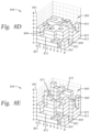
- the operations outlines above may be repeated any number of times to produce a complex and highly sophisticated 3D optical structure as illustrated in Figures 8A through 8E which will be discussed further below.
- the highly sophisticated 3D optical structures may be created by yet another technique.
- Figures 3A through 3F illustrate the second method 300 for building a 3D functional optical material level structure on a substrate using a material impregnation technique.
- the embodiment depicts the 3D stacking of optical material levels resulting in pillars of various heights on a substrate 301.
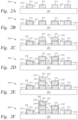
- first functional material levels (FML) 311 are formed on a top surface 302 of the substrate 301.
- the first FML 311, and each FML further described with respect to Figures 3A through 3F has a thickness, or height, of between about 20 nm to about 1 micron, such as about 200 nm.
- the first FML 311 has an outer surface 313, a first top surface 312 and a first bottom surface 315.
- the first top surface 312 of the first FML 311 is provided opposite the first bottom surface 315.
- the first bottom surface 315 being disposed on the top surface 302 of the substrate 301.
- a treatment is performed on the first FML 311 to form a first treated FML 321.
- the first treated FML 321 is a changed composition for the material of the first FML 311.
- the treatment may be performed by baking or electron volt implantation to alter the structure of the first FML 311 to yield the first treated FML 321, a more robust material suitable for stacking and substantially chemically inert to subsequent layers which may be disposed thereon.
- one or more second functional material levels (FML) 331 are formed on one or more of the first top surface 312 of the first treated FML 321.
- the second FML 331 is compatible with the first treated FML 321 such that a solvent or other chemical will not attack the underlying layer, i.e., the first treated FML 321.
- Each second FML 331 is disposed on one, but not necessarily all, of the first treated FML 321.
- the second FML 331 would not be formed on the substrate 301.
- each first treated FML 321 may not necessarily have one of the second FML 331 formed thereon, such as the first treated FML 321 provided with item number 339.
- the second FML 331 has a second outer surface 333, a second top surface 332 and a second bottom surface 335. The second bottom surface 335 being disposed on the first top surface 312 of the first treated FML 321.
- a treatment is performed on the second FML 331 to form a second treated FML 341.
- the second treated FML 341 is a changed composition for the material of the second FML 331.
- the treatment alters the structure of the second FML 331 to yield the second treated FML 341, a more robust material suitable for stacking similar, though not necessarily the same, to the first treated FML 321.
- one or more third functional material levels (FML) 351 are formed on one or more of the second top surface 332 of the second treated FML 341.
- the third FML 351 is compatible with the second treated FML 341 such that a solvent or other chemical will not attack the previous layer, i.e., the second treated FML 341.
- Each third FML 351 is disposed on one, but not necessarily all, of the second treated FML 341.
- the third FML 351 would not be formed on the substrate 301 or even the first treated FML 321.
- each second treated FML 341 may not necessarily have one of the third FML 351 formed thereon.
- a treatment is performed on the third FML 351 to form a third treated FML 361.
- the third treated FML 361 is a changed composition for the material of the third FML 351.
- the treatment alters the structure of the third FML 351 to yield the third treated FML 361, a more robust material suitable for stacking and substantially chemically inert to subsequent layers which may be disposed thereon.
- the third treated FML 361 is substantially similar to the first treated FML 321 and the second treated 341. Alternately, the third treated FML 361 may utilize a different treatment technique than either the first treated FML 321 or the second treated FML 341.
- the layers may continue to be stacked well beyond three layers. Each layer merely needs to be chemically compatible with an adjacent layer with the treatment changing the material composition to facilitate the compatibility.
- the operations outlined above may be repeated any number of times to produce a complex and highly sophisticated 3D optical structure as illustrated in Figures 8A through 8E .
- the highly sophisticated 3D optical structures may be created by yet another technique.
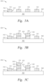
- Figures 4A through 4C illustrate the third method 400 for building 3D functional optical material level structures on a substrate using a technique of alternating pairs of materials.
- a first level may be formed from a material A and a second level may be formed from a material B, where material A after formation is compatible with material B as it is formed thereon.
- material A may be a sol-gel base material and material B can be a polymer based material.
- a solvent of material B would not dissolve or interact negatively with material A.
- Each 3D functional optical material level structure further described here in Figures 4A through 4C has a thickness, or height, of between about 20 nm to about 1 micron, such as about 200 nm.
- first functional material levels (FML) 411 are formed on a top surface 402 of the substrate 401.
- the first FML 411 has an outer surface 413, a first top surface 412 and a first bottom surface 415.
- the first top surface 412 of the first FML 411 is provided opposite the first bottom surface 415.
- the first bottom surface 415 being disposed on the top surface 402 of the substrate 401.
- the first FML 411 being formed from a first material A.
- one or more second functional material levels (FML) 421 are formed on one or more of the first top surface 412 of the first FML 411.
- Each second FML 421 is disposed on one, but not necessarily all, of the first FML 411.
- the second FML 421 has an outer surface 423, a second top surface 422 and a second bottom surface 425.
- the second FML 421 is formed from a second material B.
- the material B of the second FML 421 is compatible with the material A of the first FML 411 such that the second FML 421 does not chemically or otherwise attack the first FML 411.
- one or more third functional material levels (FML) 431 are formed on top of the one or more of the second top surface 422 of the second FML 421.
- Each third FML 431 is disposed on one, but not necessarily all, of the second FML 421.
- the third FML 431 is formed from material A.
- the third FML 431 is of the same material A as that of the first FML 411.
- the material A of the third FML 431 is compatible with the material B of the second FML 421 such that the third FML 431 does not chemically or otherwise attack the second FML 421.
- N may be equal to 4 corresponding to 4 layers of resist.
- a third resist layer 731 is formed on to the second layer having the second resist layer 721 and the second cured materials level 726.
- the third resist layer 731 may utilize a spin coating technique for applying the third resist layer 731 to the underlying layers, i.e., the second cured materials level 726 and the second resist layer 721.
- the third resist layer 731 may be applied to the underlying layers without planarization of the underlying layers.
- the material of the third resist layer 731 is substantially the same as the material of the first resist layer 711 and the second resist layer 721.
- a first layer 811 of a material 808 is provided on the substrate 801.
- the first layer 811 may be formed from a plurality of unit pieces, such as unit piece 893.
- the unit piece 893 may have a length, height and width of each between about 20 nm to about 1 micron, such as about 200 nm.
- the material 808 of the unit pieces 893 may be formed from a material compatible with the methodology utilized from above.
- the unit pieces 893 are formed from a resist material.
- the first layer 811 has a plurality of vias or voids 802 therein, i.e., absent the unit pieces 893, and may form a layer in a complicated and customized 3D structure.
- a second layer 821 of material 828 is provided on top of the material 808 of the first layer 811.
- the material 828 is available only on the top of the material 808 of the first layer 811 and not provided in the voids 802. Additionally, one or more new voids 822 are formed in the second layer 821.
- a third layer 831 of material 838 is provided on top of the material 828 of the second layer 821.
- the material 838 is available only on the top of the material 828 of the second layer 821 and not provided in the voids 802, or the material 808 of the first layer 811. Additionally, one or more new voids 832 are formed in the third layer 831.
- 3D structure 800 having four (4), eight (8), sixteen (16), thirty two (32) or more layers of material. Each layer having structures at a sub-micron scale.
- a seventh layer 871 of material is provided on the substrate 801 to form the 3D structure 800.
- 3D structure 800 may be formed with unit pieces 893 at a scale of between about 20 nm to about 1 micron, such as about 200 nm.
- the methodologies described above may advantageously form fully customizable 3D optical structure at the sub-micron level suitable for forming 3D optical operations such as holograms.
- Figure 9 shows a method 900 for forming a sub-micron 3D optical material structure on a substrate without planarization.
- Figures 10A through 10G illustrates the method 900 of Figure 9 for making symmetric 3D optical structure.
- the symmetric 3D optical structure 1000 is symmetric about a center of the symmetric 3D optical structure 1000.
- a mask material 1080 is deposited and patterned on a portion of the film stack 1008.
- step 1010 shows the mask material 1080 placed on a top surface 1011 of the film stack 1008.
- the mask material 1080 has an upper surface 1088, a bottom surface 1089, and side surfaces 1081.
- the mask material 1080 may be a photo resist or other suitable mask material.
- the formation of the mask material 1080 may be performed in a series of steps which deposit, expose, and remove unwanted mask material 1080.
- the film stack 1008 is etched down one level.
- the film stack 1008 is shown in Figure 10B at step 1020 etched one layer down. It should be appreciated that the layer, and each layer subsequently described with respect to method 1000, has a thickness, or height, of between about 20 nm to about 1 micron, such as about 200 nm.
- the mask material 1080 prevents a first layer portion 1026 of the film stack 1008 from being etched.
- the top surface 1011 of the film stack 1008 is preserved under the mask material 1080 while areas of the film stack 1008 is etched down to expose a new, i.e., second top surface 1021 one layer down.
- a side portion of the mask material 1080 is trim etched laterally by a desired distance.
- the desired distance for the trim etch may correspond to a lateral step size, for example, first layer top portion 1027.
- Figure 10C show the mask material 1080 trimmed on the side surfaces 1081 to reveal a plurality of new, i.e., second sides 1082 at step 1030.
- the trimming of the mask material 1080 makes the width thereof smaller, i.e., the distance between second sides 1082 is less than the distance between side surfaces 1081 original to the mask material 1080 prior to trimming.
- the second sides 1082 expose a first layer top portion 1027 which is no longer covered by the mask material 1080.
- a second vertical etch is performed on the mask material 1080 and optical material, i.e., film stack 1008, vertically down a 2 nd level.
- Figure 10D illustrates the film stack 1008 etched one layer further down to expose a second layer portion 1036 at step 1040.
- the mask material 1080 prevents the film stack 1008 directly thereunder, i.e., the first layer portion 1026 covered by the mask material 1080 and the second layer portion 1036 covered by the first layer portion 1026, from being etched.
- the top surface 1011 of the film stack 1008 is preserved under the mask material 1080 while areas of the film stack 1008 is etched down to expose a new, i.e., third top surface 1031, and the second layer portion 1036. Additionally, a second layer top portion 1037 is exposed while etching through the first layer top portion 1027.
- a second trim etching is performed to form a desired second lateral step size.
- the sequence of steps may be repeated.
- the trim operation (block 940) and etch operation (block 950) are repeated 'N' times to form the desired stair-step structure where not optionally blocked by the blocking layer at block 915.
- N is an integer corresponding to the number of levels for the sub-micron 3D optical structure.
- the sub-micron 3D optical structure may have N equal to the number of levels for the sub-micron 3D optical structure.
- the sub-micron 3D optical structure may have 4, 8, 16 32 or more levels.
- N is equal to 3 corresponding to 3 levels of etch and trim.
- the mask material 1080 is trimmed on the second sides 1082 to reveal a plurality of new, i.e., third sides 1083, further shrinking a width of the mask material 1080.
- the third sides 1083 again exposes the first layer top portion 1027 which is no longer covered by the mask material 1080.
- the mask material 1080 is stripped from the film stack 1008.
- the optional blocking material is stripped as well if it is present.
- the mask material 1080 is stripped off to reveal the 3D optical structure 1099.
- a profile for the third layer portion 1046, the second layer portion 1036, and the first layer portion 1026 is symmetric about a center of the 3D optical structure 1099. It should be appreciated that the preceding steps of etching and trimming can be repeated any number of times to produce symmetrical 3D structures having a multitude of layers prior to stripping the mask material 1080 wherein each layer has a thickness, or height, of between about 20 nm to about 1 micron, such as about 200 nm. It should also be appreciated that the trimming of the sides for the mask material 1080 may optionally be skipped for one or more layers where a straight vertical wall is desired over a stepped wall.
- a mask material may optionally be added to cover selected stepped regions, and etching down the originally blocked area to a lower step level. This operation is described with respect to block 1140 shown in Figure 11D below.
- the 3D optical structure 1099 may optionally be used as a master for imprinting the inverse shape in an optical material or stack.
- the 3D optical structure 1000 is shown symmetrical but may incorporate a stepped structure through the use of the optional blocked material. It should be appreciated that the steps may be irregular as will be further discussed below with respect to Figures 12A through 13C .
- Figures 11A through 11E illustrate a method 1100 for making a one or more stepped sided 3D optical structure 1199.
- a film stack 1108 disposed on a substrate 1101 is provided for method 1100.
- a hardmask 1171 is disposed on a portion of a top surface 1102 of the film stack 1108.
- a mask material 1180 is placed on a portion of the hardmask 1171 and the top surface 1102 of the film stack 1108.
- the hardmask 1171 extends halfway along a bottom surface of the mask material 1180.
- the hardmask 1171 barely extends under the mask material 1180.
- the mask material 1180 may be a photoresist and operate similarly to mask material 1080 disclosed with respect to the method 1000 above in Figures 10A through 10G .
- the mask material 1180 is stripped off to reveal a 3D step structure 1181.
- the film stack 1108 was etched and the mask material 1180 was trimmed prior to block 1120 over a series of steps as illustrated in Figures 10A to 10G .
- the hardmask 1171 prevents any etching of the underlying film stack 1108.
- the top surface 1102 is etched down 3 layers to a fourth top surface 1105.
- the steps illustrated in method 1000 only produces a portion, i.e., the 3D step structure 1181, in which the etch process was blocked or prevented by the hardmask 1171.
- the 3D step structure 1181 has a first step 1126, a second step 1136 and a third step 1146.
- Each of the first step 1126, the second step 1136 and the third step 1146 has a thickness, or height, of between about 20 nm to about 1 micron, such as about 200 nm.
- the first step 1126 may extend from the second step 1136 and the second step 1136 may extend from the third step 1146 by a distance of between about 20 nm to about 1 micron, such as about 200 nm.
- the hardmask 1171 is stripped from the film stack 1108.
- the hardmask 1171 may be selectively removed leaving the top surface 1102, the 3D step structure 1181 and the fourth top surface 1105, i.e., the film stack 1108.
- a second mask material 1190 is disposed on the 3D step structure 1181 and the fourth top surface 1105.
- the second mask material covers a top of the 3D step structure 1181.
- the top may be of any suitable length. In one embodiment, the top has a single unit length of between about 20 nm to about 1 micron, such as about 200 nm.
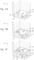
- Figure 13B illustrates a square frustum 1320 having at least one substantially flat side.
- the square frustum 1320 is a three dimensional solid that has four congruent trapezoids for its front side 1322, a far side (not visible), a first side 1321 and a second side 1323.
- the square frustum 1320 has substantially planar a top 1324 and a bottom (not visible) each connecting the corresponding sides of the front side 1322, the far side, the first side 1321 and the second side 1323.
- Each of the first side 1321, the second side 1323, the front side 1322 and the far side may be angled from the bottom to the top 1324 such that the plan area of the bottom is larger than the plan area of the top 1324.
- One, two or three of the first side 1321, the second side 1323, the front side 1322 and the far side may have grating corresponding to sub-micron steps in the formation thereof. Additionally, one, two or three of the first side 1321, the second side 1323, the front side 1322 and the far side may be substantially flat without grating, i.e., structures formed therein. For example, a callout portion 1328 shows grating 1327 thereon the first side and far side while the front side 1322 and the second side 1323 are substantially vertical and without grating.
- the front side 1322 and second side 1323 may have been formed with a blocking material preventing etching and the formation of grating, i.e., the steps.
- Figure 13C illustrates a triangular pyramid 1330 having at least one substantially flat side.
- the triangular pyramid 1330 is a three dimensional solid that has three congruent triangles for its front side 1332, a far side 1333, and a first side 1331.
- the triangular pyramid 1330 has an apex at a top 1381 and a substantially planar bottom (not visible) each connecting the corresponding sides of the front side 1332 the far side 1333, and the first side 1331.
- Each of the first side 1331, the far side 1333, and the front side 1332 may be angled from the bottom to the top 1334 forming the apex at the top 1334.
- first side 1331, the far side 1333 and the front side 1332 may have grating corresponding to sub-micron steps in the formation thereof. Additionally, one or two of the first side 1331, the far side 1333 and the front side 1332 may be substantially flat without grating, i.e., structures formed therein. For example, a callout 1338 shows grating 1337 thereon the first side 1312 and the far side 1333 while the front side 1332 is substantially vertical and without grating.
- the front side 1332 may have been formed with a blocking material preventing etching and the formation of grating, i.e., the steps.
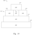
- Figure 14 illustrates another embodiment for the 3D optical material level structure 1400 formed on a diffractive optics element formed using the repetitive coating and exposure technique, the 3D optical material level structure 1400 having a gap therein.
- the 3D functional optical material level structure 1400 may have a first level 1410 disposed on the substrate 1401.
- the first level 1410 may be patterned and exposed in a lithography operation.
- a plurality of second level features 1420 may be formed on a top surface 1411 of the first level feature 1410.
- a resist material may be spun onto the first level features 1410.
- the second level features 1420 may be exposed in a lithography operation to form a first exposed portion 1422, a non-exposed resist portion 1423 and a second exposed portion 1422.
- a third level 1430 may be spun on top the second level features 1420.
- the third level features may be patterned and exposed to form exposed features 1431 therein.
- the 3D functional optical material level structure 1400 may then be developed to remove all resist that was not patterned and exposed in the lithography operation, for example, non-exposed resist portion 1423.
- the resultant structure may generate features of varying width and void therebetween. For example, a void (no material) now exists where non-exposed resist portion 1423 and the third level feature 1431 is disposed on top, or suspended, by a first upper surface 1426 of the first exposed portion 1422 and a second upper surface 1425 of the second exposed portion 1422.
- each portion forming the final 3D functional optical material level structure 1400 is fully customizable and merely a function of the thickness of material spun on to a lower level and the feature size in the pattern used in one or more lithography operations.
- fully customizable 3D functional optical material level structure 1400 can be formed on a diffractive optics element at a sub-micron scale.
- Figure 15A through 15I illustrates a method for building fully customizable 3D functional optical material level structure 1500 on a substrate 1501 using the trim etch technique discussed above.
- the method starts at block 1510, as shown in Figure 15A , wherein an optical material stack, i.e., film stack 1508, to be patterned into a diffractive optics element is deposited on a substrate 1501.
- the substrate 1501 may be a single optical material or diffractive optics element.
- the depositing material may be used to make a master for forming a 3D optical structure wherein the master is transposed from the final 3D optical structure.
- the film stack 1508 may be a resist material for forming features in the substrate below or the film stack 1508 may be a plurality of optical materials suitable to form the 3D functional optical material level structure 1500.
- the film stack 1508 is etched down one level.
- the layer, and each layer subsequently described with respect to the method described above may have a thickness, or height, of between about 20 nm to about 1 micron, such as about 200 nm.
- the mask material 1509 prevents a first layer portion 1526 of the film stack 1508 from being etched.
- the top surface 1511 of the film stack 1508 is preserved under the mask material 1509 while other areas of the film stack 1508 is etched down to expose a new, i.e., second top surface 1521 one layer down.
- the right side surface 1581 and the left side surface 1582 of the mask material 1509 is trimmed, i.e., etched laterally, by a desired distance.
- the desired distance for the trim may correspond to a lateral step size, for example, a first layer top portion 1527.
- the right side surface 1581 and the left side surface 1582 are trimmed away to reveal a plurality of new, i.e., a second left sides 1584 and a second right side 1583.
- the trimming of the mask material 1509 makes the width thereof smaller, i.e., the distance between the right side surface 1581 and the left side surface 1582 is greater than the distance between the second right side surface 1583 and the second left side surface 1584 of the mask material 1509 prior to trimming.
- the second right side surface 1583 and the second left side surface 1584 expose a first layer top portion 1527 which is no longer covered by the mask material 1509.
- the mask material 1509 may be trimmed along each of the sides between about 20 nm to about 1 micron, such as about 200 nm. Thus making the first layer top portion 1527 between about 20 nm to about 1 micron from a respective side of the mask material 1509. Alternately, the mask material 1509 is selectively trimmed etched, for example by directional etching.
- a second vertical etch is performed on the optical material, i.e., film stack 1508, vertically down a 2 nd level.
- the film stack 1508 is etched one layer further down to expose a second layer portion 1536 and a second layer top portion 1537 while etching through the first layer top portion 1527.
- the mask material 1509 prevents the film stack 1508 directly thereunder, i.e., the first layer portion 1526 covered by the mask material 1509 and the second layer portion 1536 covered by the first layer portion 1526, from being etched.
- the top surface 1511 of the film stack 1508 is preserved under the mask material 1509 while other areas of the film stack 1508 is etched down to expose a new, i.e., third top surface 1531, the second layer top portion 1537, and the second layer portion 1536.
- the sequence of steps above may be repeated any number of times to produce the desired structure.
- the trim operation at block 1530 and etch operation at block 1540 are repeated 'N' times to form the desired stair-step structure having optional flat sections disposed throughout the structure.
- N is an integer corresponding to the number of levels for the sub-micron 3D optical structure.
- the sub-micron 3D optical structure may have N equal to the number of levels for the sub-micron 3D optical structure.
- the sub-micron 3D optical structure may have 4, 8, 16 32 or more levels.
- N is equal to 3 corresponding to 3 levels of etch and trim.
- a third trim etching is performed to form a desired third lateral step size.
- the third trim operation may be a directional etch operation targeting one or more particular sides of the mask material 1509.
- the directional etch may trim the second right side 1583 to reveal a third right side 1585 while leaving second left sides 1584 intact.
- the trim operation may reveal the first layer top portion 1527 yet again on the right side 1591 while leaving the mask material 1509 covering the first layer 1526 on the left side 1592.
- the film stack 1508 is etched further one layer down to expose a third layer portion 1546.
- the mask material 1509 prevents the film stack 1508 directly thereunder from being etched.
- the top surface 1511 of the film stack 1508 is preserved under the mask material 1509 while areas of the film stack 1508 is etched down to expose a new, i.e., fourth top surface 1541 and a third layer top portion 1547 of the third layer portion 1546.
- the left side 1592 is substantially vertical up from the third top layer portion 1547 while the rights side 1591 has a series of steps corresponding to the third layer portion 1546, the second layer portion 1536 and the first layer portion 1526.
- the film stack 1508 is etched further one layer down to expose a fourth layer portion 1556.
- the mask material 1509 prevents the film stack 1508 directly thereunder from being etched.
- the top surface 1511 of the film stack 1508 is preserved under the mask material 1509 while areas of the film stack 1508 is etched down to expose a new fifth top surface 1551 and a fourth layer top portion 1557 of the fourth layer portion 1556.
- the left side 1592 now has a single step from the second top layer portion 1537 while the right side 1591 has a series of steps corresponding to the fourth layer portion 1556, the third layer portion 1546, the second layer portion 1536 and the first layer portion 1526.
- the mask material 1509 is stripped from the film stack 1508 to reveal the 3D optical structure 1500.
- a profile for the fourth layer portion 1556, the third layer portion 1546, the second layer portion 1536, and the first layer portion 1526 is asymmetric about a center of the 3D optical structure 1500. It should be appreciated that the preceding steps of etching and trimming can be repeated any number of times to produce symmetrical 3D structures having a multitude of layers prior to stripping the mask material 1509 wherein each layer has a thickness, or height, of between about 20 nm to about 1 micron, such as about 200 nm. It should also be appreciated that the trimming of the sides for the mask material 1509 may optionally be skipped for one or more layers where a straight vertical wall is desired over a stepped wall.
- the stackable optical material 711 is optionally baked.
- the exposure and baking process 719 results in the stackable optical material 711 forming a plurality of first cured materials 716 in the locations which were exposed through the mask and then baked.
- a second layer of optical material 721 is deposited on the stackable optical material 711, inclusive of the first cured materials 716.
- the second layer of optical material 721 may be spin coated onto the stackable optical material 711 or formed by other suitable techniques.
- the second layer of optical material 721 is exposed to form a pattern therein.
- the pattern is designed to produce the second level of the multi-level optical structure, or in the case of imprint, provide the second level in construction of the inverse pattern for the master to be used in the manufacture of multiple optical structures.
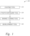
- the step 1625 for depositing optical material on an underlying layer, the step 1630 for exposing the optical material to form a pattern therein, and the step 1635 for optionally baking the patterned optical material are repeating for N levels to produce a multi-level 3D functional optical material level structure.
- the 3D functional optical material level structure has N levels such as 4 levels, 8 levels, 16 levels, 32 levels, or maybe more.
- the exposed and cured regions of the N patterns on N layers are simultaneously developed.
- the development removes the un-patterned material from the 3D functional optical material level structure, or master.
- the developed 3D structure, or master is formed from the cured materials layers left behind on the substrate 701.
- the master left behind from the development step above is used for imprinting the inverse shape in an optical material or stack.
- the optical material may be repeatedly and accurately used to form a plurality of 3D functional optical material level structures.
- the methods described above provide techniques having reduced steps for building sub-micron devices.
- the techniques require fewer operations (such as planarization) saving raw materials, machine operational costs, and time.
- the 3D optical devices may be symmetrical or asymmetrical and are formed from units having dimensions between about 20 nm to about 1 micron, such as about 200 nm in each of the coordinate directions, such as in an X, Y and Z direction.
- the 3D optical devices therefore can be made small enough to be utilized for creating high resolution holographic images from small devices.
Landscapes
- Physics & Mathematics (AREA)
- General Physics & Mathematics (AREA)
- Optics & Photonics (AREA)
- Engineering & Computer Science (AREA)
- Chemical & Material Sciences (AREA)
- Materials Engineering (AREA)
- Manufacturing & Machinery (AREA)
- Mechanical Engineering (AREA)
- Diffracting Gratings Or Hologram Optical Elements (AREA)
- Photosensitive Polymer And Photoresist Processing (AREA)
- Exposure And Positioning Against Photoresist Photosensitive Materials (AREA)
- Holo Graphy (AREA)
Claims (5)
- Procédé de formation d'une structure de matériau optique 3D submicronique (1000) sur un élément d'optique diffractive sans planarisation, le procédé comprenant :A) le dépôt d'un empilement de matériaux à modeler sur un substrat (1001) ;B) le dépôt et le modelage d'un matériau de masque (1080) sur une partie de l'empilement de matériaux ;C) la gravure de l'empilement de matériaux d'un niveau vers le bas ;D) le rognage d'une partie latérale du matériau de masque (1080) ;E) la gravure de l'empilement de matériaux d'un niveau supplémentaire vers le bas ;F) la répétition de D et E 'N' fois ;G) l'enlèvement du matériau de masque (1080) de l'empilement de matériaux ; etH) le fait de sauter le rognage des côtés du matériau de masque (1080) pour une ou plusieurs opérations de gravure.
- Procédé selon la revendication 1, comprenant en outre :
le dépôt et le modelage par lithographie d'une couche de blocage conçue pour résister à une gravure de l'empilement de matériaux. - Procédé selon la revendication 2, dans lequel, en réponse au modelage de la couche de blocage, le procédé comprend en outre :
le développement de la couche de blocage et le retrait du matériau non modelé. - Procédé selon la revendication 3, comprenant en outre :
l'enlèvement de la couche de blocage. - Procédé selon la revendication 1, comprenant en outre :
l'utilisation de l'empilement de matériaux gravés comme matrice pour imprimer une forme inverse de l'empilement de matériaux gravés dans un matériau ou un empilement optique.
Priority Applications (1)
| Application Number | Priority Date | Filing Date | Title |
|---|---|---|---|
| EP25186974.9A EP4606560A3 (fr) | 2018-03-06 | 2019-03-05 | Procédé de construction d'une structure d'empilement de matériau optique fonctionnel 3d |
Applications Claiming Priority (2)
| Application Number | Priority Date | Filing Date | Title |
|---|---|---|---|
| US201862639475P | 2018-03-06 | 2018-03-06 | |
| PCT/US2019/020813 WO2019173383A1 (fr) | 2018-03-06 | 2019-03-05 | Procédé de construction d'une structure d'empilement de matériau optique fonctionnel 3d |
Related Child Applications (1)
| Application Number | Title | Priority Date | Filing Date |
|---|---|---|---|
| EP25186974.9A Division EP4606560A3 (fr) | 2018-03-06 | 2019-03-05 | Procédé de construction d'une structure d'empilement de matériau optique fonctionnel 3d |
Publications (3)
| Publication Number | Publication Date |
|---|---|
| EP3762778A1 EP3762778A1 (fr) | 2021-01-13 |
| EP3762778A4 EP3762778A4 (fr) | 2022-03-09 |
| EP3762778B1 true EP3762778B1 (fr) | 2025-07-09 |
Family
ID=67842516
Family Applications (2)
| Application Number | Title | Priority Date | Filing Date |
|---|---|---|---|
| EP25186974.9A Pending EP4606560A3 (fr) | 2018-03-06 | 2019-03-05 | Procédé de construction d'une structure d'empilement de matériau optique fonctionnel 3d |
| EP19763340.7A Active EP3762778B1 (fr) | 2018-03-06 | 2019-03-05 | Procédé de construction d'une structure d'empilement de matériau optique fonctionnel 3d |
Family Applications Before (1)
| Application Number | Title | Priority Date | Filing Date |
|---|---|---|---|
| EP25186974.9A Pending EP4606560A3 (fr) | 2018-03-06 | 2019-03-05 | Procédé de construction d'une structure d'empilement de matériau optique fonctionnel 3d |
Country Status (7)
| Country | Link |
|---|---|
| US (3) | US11187836B2 (fr) |
| EP (2) | EP4606560A3 (fr) |
| JP (1) | JP7225256B2 (fr) |
| KR (1) | KR102585150B1 (fr) |
| CN (2) | CN111819497B (fr) |
| TW (3) | TWI749299B (fr) |
| WO (1) | WO2019173383A1 (fr) |
Families Citing this family (9)
| Publication number | Priority date | Publication date | Assignee | Title |
|---|---|---|---|---|
| US11662524B2 (en) * | 2020-03-13 | 2023-05-30 | Applied Materials, Inc. | Forming variable depth structures with laser ablation |
| CN116097132A (zh) | 2020-09-03 | 2023-05-09 | 尼尔技术有限公司 | 衍射光学元件及用于生产衍射光学元件的样板工具 |
| EP4266092A4 (fr) * | 2020-12-18 | 2024-04-17 | Fujikura Ltd. | Système de calcul optique |
| EP4296770A4 (fr) * | 2021-02-19 | 2025-01-08 | Fujikura Ltd. | Dispositif de calcul optique et procédé de calcul optique |
| EP4099092B1 (fr) * | 2021-06-02 | 2023-03-15 | Joanneum Research Forschungsgesellschaft mbH | Procédé lithographique destiné à l'estampage des microstructures tridimensionnelles à des hauteurs de structure surdimensionnées dans un matériau porteur |
| CN113985700B (zh) * | 2021-11-18 | 2023-08-29 | 业成科技(成都)有限公司 | 光波导与显示装置的制作方法及其使用的光罩 |
| US20250117561A1 (en) * | 2023-10-06 | 2025-04-10 | Applied Materials, Inc. | Structure and technique of photo-defined semiconductor device with selective dielectric constant reduction |
| US20250244531A1 (en) * | 2023-12-22 | 2025-07-31 | Snap Inc. | Zoned depth structures |
| US20250306276A1 (en) * | 2024-03-29 | 2025-10-02 | Applied Materials, Inc. | Process integration flow for staircase gratings |
Family Cites Families (42)
| Publication number | Priority date | Publication date | Assignee | Title |
|---|---|---|---|---|
| US4985374A (en) * | 1989-06-30 | 1991-01-15 | Kabushiki Kaisha Toshiba | Making a semiconductor device with ammonia treatment of photoresist |
| JPH0827407B2 (ja) | 1993-06-02 | 1996-03-21 | 日本電気株式会社 | 微細グレーティング形成方法 |
| US5631762A (en) * | 1993-06-04 | 1997-05-20 | Hitachi Koki Co., Ltd. | Multi-beam generating element and optical printing apparatus therewith |
| US5566024A (en) * | 1993-12-23 | 1996-10-15 | Xerox Corporation | Beam separation control and beam splitting by single blazed binary diffraction optical element |
| US5487962A (en) * | 1994-05-11 | 1996-01-30 | Rolfson; J. Brett | Method of chromeless phase shift mask fabrication suitable for auto-cad layout |
| JPH11237503A (ja) * | 1997-12-03 | 1999-08-31 | Canon Inc | 回折光学素子及びそれを有する光学系 |
| JP2000206321A (ja) * | 1999-01-19 | 2000-07-28 | Canon Inc | 回折光学素子、回折光学素子を備えた光学系、回折光学素子の製造方法、回折光学素子を備えた光学系を含む露光装置、及び露光装置を用いたデバイスの製造方法 |
| JP4390119B2 (ja) * | 2000-04-14 | 2009-12-24 | キヤノン株式会社 | 回折光学素子の製造方法 |
| US6653244B2 (en) * | 2001-09-19 | 2003-11-25 | Binoptics Corporation | Monolithic three-dimensional structures |
| US6905618B2 (en) * | 2002-07-30 | 2005-06-14 | Agilent Technologies, Inc. | Diffractive optical elements and methods of making the same |
| WO2005093466A1 (fr) * | 2004-03-26 | 2005-10-06 | Sony Corporation | Substrat de matrice a microlentilles et procede de fabrication de celui-ci |
| US20060050391A1 (en) * | 2004-08-10 | 2006-03-09 | Johan Backlund | Structured-groove diffraction granting and method for control and optimization of spectral efficiency |
| WO2006120720A1 (fr) * | 2005-05-02 | 2006-11-16 | Oki Electric Industry Co., Ltd. | Procédé de fabrication d’un élément optique à diffraction |
| JP5048930B2 (ja) * | 2005-06-08 | 2012-10-17 | ラピスセミコンダクタ株式会社 | 回折光学素子,および,回折光学素子の製造方法 |
| JP5046565B2 (ja) * | 2005-06-10 | 2012-10-10 | 株式会社半導体エネルギー研究所 | 半導体装置の作製方法 |
| EP1880830B1 (fr) * | 2006-07-19 | 2011-12-21 | Envisiontec GmbH | Procédé et dispositif pour la fabrication d'un article tridimensionel, un ordinateur et un support d'information associés |
| WO2008115600A1 (fr) * | 2007-03-21 | 2008-09-25 | Olambda, Inc. | Couche de masque dur multi-matière ou à motifs préformés à utiliser avec une photolithographie multi-motifs |
| US8709951B2 (en) * | 2007-07-19 | 2014-04-29 | Texas Instruments Incorporated | Implementing state-of-the-art gate transistor, sidewall profile/angle control by tuning gate etch process recipe parameters |
| JP5339975B2 (ja) * | 2008-03-13 | 2013-11-13 | キヤノン株式会社 | X線位相イメージングに用いられる位相格子、該位相格子を用いたx線位相コントラスト像の撮像装置、x線コンピューター断層撮影システム |
| US8636496B2 (en) * | 2008-05-05 | 2014-01-28 | Georgia Tech Research Corporation | Systems and methods for fabricating three-dimensional objects |
| CN102017791B (zh) * | 2009-05-12 | 2013-03-06 | 松下电器产业株式会社 | 板、发光装置及板的制造方法 |
| JP5274393B2 (ja) * | 2009-06-30 | 2013-08-28 | アルバック成膜株式会社 | ハーフトーンマスクの製造方法 |
| US7786020B1 (en) * | 2009-07-30 | 2010-08-31 | Hynix Semiconductor Inc. | Method for fabricating nonvolatile memory device |
| JP2011129874A (ja) * | 2009-11-19 | 2011-06-30 | Toshiba Corp | パターン形成方法及びパターン形成装置 |
| TWI461833B (zh) * | 2010-03-15 | 2014-11-21 | Hoya股份有限公司 | 多調式光罩、多調式光罩之製造方法及圖案轉印方法 |
| JP2013077665A (ja) * | 2011-09-30 | 2013-04-25 | Toppan Printing Co Ltd | パターン形成方法及びパターン形成体 |
| FR2981460B1 (fr) * | 2011-10-18 | 2016-06-24 | Commissariat Energie Atomique | Procede de realisation d'un dispositif optique refractif ou diffractif |
| KR101890781B1 (ko) | 2012-03-30 | 2018-08-22 | 어플라이드 머티어리얼스, 인코포레이티드 | 터치 패널에서 이용하기 위한 투명 바디 및 그 제조 방법 및 장치 |
| US20140087016A1 (en) * | 2012-09-26 | 2014-03-27 | HGST Netherlands B.V. | Nanoimprinting master template and method for making |
| TWI497690B (zh) | 2013-01-11 | 2015-08-21 | Macronix Int Co Ltd | 三維堆疊半導體裝置及其製造方法 |
| US9240359B2 (en) * | 2013-07-08 | 2016-01-19 | Applied Materials, Inc. | 3D NAND staircase CD control by using interferometric endpoint detection |
| EP3078482B1 (fr) * | 2013-12-03 | 2019-05-22 | Prismlab China Ltd. | Dispositif d'impression 3d à photodurcissement et son système d'imagerie |
| JP6313591B2 (ja) * | 2013-12-20 | 2018-04-18 | キヤノン株式会社 | インプリント装置、異物除去方法及び物品の製造方法 |
| US10046589B2 (en) * | 2014-05-16 | 2018-08-14 | Ccl Secure Pty Ltd | Hybrid security device for security document or token |
| CN103969724B (zh) * | 2014-05-23 | 2016-08-17 | 厦门大学 | 一种衍射光学元件的制作方法 |
| KR20160045340A (ko) | 2014-10-17 | 2016-04-27 | 에스케이하이닉스 주식회사 | 3차원 비휘발성 메모리 장치 |
| JP2018508835A (ja) | 2015-01-05 | 2018-03-29 | マーシュピアル ホールディングス エルエルシー | マルチトーンレベルフォトマスク{multi−tone amplitude photomask} |
| CN107250965A (zh) | 2015-02-12 | 2017-10-13 | 应用材料公司 | 适于用于光电装置中的层堆叠、光电装置、以及适于用于光电装置中的层堆叠的制造方法 |
| JP6823374B2 (ja) * | 2016-03-10 | 2021-02-03 | キヤノン株式会社 | パターンの欠陥の分析を行う方法、インプリント装置、及び物品の製造方法 |
| US9997555B2 (en) * | 2016-08-02 | 2018-06-12 | The Government Of The United States Of America, As Represented By The Secretary Of The Navy | Fabrication method for digital etching of nanometer-scale level structures |
| US10473834B2 (en) * | 2016-11-21 | 2019-11-12 | Stmicroelectronics (Research & Development) Limited | Wafer level microstructures for an optical lens |
| US10802185B2 (en) * | 2017-08-16 | 2020-10-13 | Lumentum Operations Llc | Multi-level diffractive optical element thin film coating |
-
2019
- 2019-03-05 CN CN201980017035.7A patent/CN111819497B/zh active Active
- 2019-03-05 CN CN202410176783.2A patent/CN118091808A/zh active Pending
- 2019-03-05 WO PCT/US2019/020813 patent/WO2019173383A1/fr not_active Ceased
- 2019-03-05 US US16/293,354 patent/US11187836B2/en active Active
- 2019-03-05 EP EP25186974.9A patent/EP4606560A3/fr active Pending
- 2019-03-05 EP EP19763340.7A patent/EP3762778B1/fr active Active
- 2019-03-05 KR KR1020207028554A patent/KR102585150B1/ko active Active
- 2019-03-05 JP JP2020546129A patent/JP7225256B2/ja active Active
- 2019-03-06 TW TW108107422A patent/TWI749299B/zh active
- 2019-03-06 TW TW110121640A patent/TWI809421B/zh active
- 2019-03-06 TW TW110141747A patent/TWI809558B/zh active
-
2021
- 2021-11-24 US US17/456,507 patent/US20220082738A1/en active Pending
-
2024
- 2024-02-12 US US18/439,434 patent/US20240184024A1/en active Pending
Also Published As
| Publication number | Publication date |
|---|---|
| KR20200119345A (ko) | 2020-10-19 |
| TW202210939A (zh) | 2022-03-16 |
| TWI809558B (zh) | 2023-07-21 |
| JP2021516367A (ja) | 2021-07-01 |
| EP4606560A2 (fr) | 2025-08-27 |
| EP4606560A3 (fr) | 2025-11-26 |
| TWI749299B (zh) | 2021-12-11 |
| US20220082738A1 (en) | 2022-03-17 |
| CN111819497A (zh) | 2020-10-23 |
| KR102585150B1 (ko) | 2023-10-06 |
| CN111819497B (zh) | 2024-02-27 |
| CN118091808A (zh) | 2024-05-28 |
| TW201945842A (zh) | 2019-12-01 |
| US20190278005A1 (en) | 2019-09-12 |
| US20240184024A1 (en) | 2024-06-06 |
| JP7225256B2 (ja) | 2023-02-20 |
| TW202142954A (zh) | 2021-11-16 |
| WO2019173383A1 (fr) | 2019-09-12 |
| TWI809421B (zh) | 2023-07-21 |
| US11187836B2 (en) | 2021-11-30 |
| EP3762778A1 (fr) | 2021-01-13 |
| EP3762778A4 (fr) | 2022-03-09 |
Similar Documents
| Publication | Publication Date | Title |
|---|---|---|
| US20240184024A1 (en) | Method of building a 3d functional optical material stacking structure | |
| US11347145B2 (en) | Pre-patterned lithography templates | |
| TWI608292B (zh) | 使用接枝聚合物材料以便基板圖案化 | |
| RU2462412C2 (ru) | Способ формирования наноразмерного рисунка на подложке (варианты) и структура с рисунком, состоящая из наноразмерных самособранных самовыстроенных структур | |
| US6749997B2 (en) | Method for providing an arbitrary three-dimensional microstructure in silicon using an anisotropic deep etch | |
| TWI486705B (zh) | 使用自組聚合物之微影技術 | |
| JP5758363B2 (ja) | パターン形成方法 | |
| WO2014152435A1 (fr) | Nanostructures programmables à motif dense à facteur de forme élevé utilisant une attaque chimique assistée par métal | |
| JP2016513594A (ja) | ブロック共重合体の自己組織化によって基板上にリソグラフィフィーチャを提供する方法 | |
| US6841339B2 (en) | Silicon micro-mold and method for fabrication | |
| US6798862B2 (en) | X-ray mask and method for providing same | |
| WO2018222915A1 (fr) | Formation de motif bidimensionnel de couche de circuit intégré par implantation ionique inclinée | |
| Morales | Silicon micro-mold and method for fabrication |
Legal Events
| Date | Code | Title | Description |
|---|---|---|---|
| STAA | Information on the status of an ep patent application or granted ep patent |
Free format text: STATUS: THE INTERNATIONAL PUBLICATION HAS BEEN MADE |
|
| PUAI | Public reference made under article 153(3) epc to a published international application that has entered the european phase |
Free format text: ORIGINAL CODE: 0009012 |
|
| STAA | Information on the status of an ep patent application or granted ep patent |
Free format text: STATUS: REQUEST FOR EXAMINATION WAS MADE |
|
| 17P | Request for examination filed |
Effective date: 20201001 |
|
| AK | Designated contracting states |
Kind code of ref document: A1 Designated state(s): AL AT BE BG CH CY CZ DE DK EE ES FI FR GB GR HR HU IE IS IT LI LT LU LV MC MK MT NL NO PL PT RO RS SE SI SK SM TR |
|
| AX | Request for extension of the european patent |
Extension state: BA ME |
|
| DAV | Request for validation of the european patent (deleted) | ||
| DAX | Request for extension of the european patent (deleted) | ||
| RIC1 | Information provided on ipc code assigned before grant |
Ipc: G02B 5/18 20060101ALI20211021BHEP Ipc: H01L 21/324 20060101ALI20211021BHEP Ipc: H01L 21/02 20060101ALI20211021BHEP Ipc: H01L 21/027 20060101ALI20211021BHEP Ipc: G03F 7/16 20060101ALI20211021BHEP Ipc: G03F 7/00 20060101ALI20211021BHEP Ipc: G03F 7/20 20060101AFI20211021BHEP |
|
| A4 | Supplementary search report drawn up and despatched |
Effective date: 20220207 |
|
| RIC1 | Information provided on ipc code assigned before grant |
Ipc: B29C 64/124 20170101ALI20220201BHEP Ipc: G02B 5/18 20060101ALI20220201BHEP Ipc: H01L 21/324 20060101ALI20220201BHEP Ipc: H01L 21/02 20060101ALI20220201BHEP Ipc: H01L 21/027 20060101ALI20220201BHEP Ipc: G03F 7/16 20060101ALI20220201BHEP Ipc: G03F 7/00 20060101ALI20220201BHEP Ipc: G03F 7/20 20060101AFI20220201BHEP |
|
| GRAP | Despatch of communication of intention to grant a patent |
Free format text: ORIGINAL CODE: EPIDOSNIGR1 |
|
| STAA | Information on the status of an ep patent application or granted ep patent |
Free format text: STATUS: GRANT OF PATENT IS INTENDED |
|
| RIC1 | Information provided on ipc code assigned before grant |
Ipc: B29C 64/124 20170101ALI20240829BHEP Ipc: G02B 5/18 20060101ALI20240829BHEP Ipc: H01L 21/324 20060101ALI20240829BHEP Ipc: H01L 21/02 20060101ALI20240829BHEP Ipc: H01L 21/027 20060101ALI20240829BHEP Ipc: G03F 7/16 20060101ALI20240829BHEP Ipc: G03F 7/00 20060101ALI20240829BHEP Ipc: G03F 7/20 20060101AFI20240829BHEP |
|
| INTG | Intention to grant announced |
Effective date: 20240925 |
|
| GRAJ | Information related to disapproval of communication of intention to grant by the applicant or resumption of examination proceedings by the epo deleted |
Free format text: ORIGINAL CODE: EPIDOSDIGR1 |
|
| STAA | Information on the status of an ep patent application or granted ep patent |
Free format text: STATUS: REQUEST FOR EXAMINATION WAS MADE |
|
| GRAP | Despatch of communication of intention to grant a patent |
Free format text: ORIGINAL CODE: EPIDOSNIGR1 |
|
| STAA | Information on the status of an ep patent application or granted ep patent |
Free format text: STATUS: GRANT OF PATENT IS INTENDED |
|
| INTC | Intention to grant announced (deleted) | ||
| INTG | Intention to grant announced |
Effective date: 20250206 |
|
| GRAS | Grant fee paid |
Free format text: ORIGINAL CODE: EPIDOSNIGR3 |
|
| GRAA | (expected) grant |
Free format text: ORIGINAL CODE: 0009210 |
|
| STAA | Information on the status of an ep patent application or granted ep patent |
Free format text: STATUS: THE PATENT HAS BEEN GRANTED |
|
| AK | Designated contracting states |
Kind code of ref document: B1 Designated state(s): AL AT BE BG CH CY CZ DE DK EE ES FI FR GB GR HR HU IE IS IT LI LT LU LV MC MK MT NL NO PL PT RO RS SE SI SK SM TR |
|
| REG | Reference to a national code |
Ref country code: GB Ref legal event code: FG4D |
|
| REG | Reference to a national code |
Ref country code: CH Ref legal event code: EP |
|
| REG | Reference to a national code |
Ref country code: IE Ref legal event code: FG4D |
|
| REG | Reference to a national code |
Ref country code: DE Ref legal event code: R096 Ref document number: 602019072306 Country of ref document: DE |
|
| REG | Reference to a national code |
Ref country code: NL Ref legal event code: MP Effective date: 20250709 |
|
| PG25 | Lapsed in a contracting state [announced via postgrant information from national office to epo] |
Ref country code: PT Free format text: LAPSE BECAUSE OF FAILURE TO SUBMIT A TRANSLATION OF THE DESCRIPTION OR TO PAY THE FEE WITHIN THE PRESCRIBED TIME-LIMIT Effective date: 20251110 |
|
| PG25 | Lapsed in a contracting state [announced via postgrant information from national office to epo] |
Ref country code: NL Free format text: LAPSE BECAUSE OF FAILURE TO SUBMIT A TRANSLATION OF THE DESCRIPTION OR TO PAY THE FEE WITHIN THE PRESCRIBED TIME-LIMIT Effective date: 20250709 |
|
| REG | Reference to a national code |
Ref country code: AT Ref legal event code: MK05 Ref document number: 1812373 Country of ref document: AT Kind code of ref document: T Effective date: 20250709 |
|
| PG25 | Lapsed in a contracting state [announced via postgrant information from national office to epo] |
Ref country code: IS Free format text: LAPSE BECAUSE OF FAILURE TO SUBMIT A TRANSLATION OF THE DESCRIPTION OR TO PAY THE FEE WITHIN THE PRESCRIBED TIME-LIMIT Effective date: 20251109 |
|
| PG25 | Lapsed in a contracting state [announced via postgrant information from national office to epo] |
Ref country code: NO Free format text: LAPSE BECAUSE OF FAILURE TO SUBMIT A TRANSLATION OF THE DESCRIPTION OR TO PAY THE FEE WITHIN THE PRESCRIBED TIME-LIMIT Effective date: 20251009 |
|
| REG | Reference to a national code |
Ref country code: LT Ref legal event code: MG9D |
|
| PG25 | Lapsed in a contracting state [announced via postgrant information from national office to epo] |
Ref country code: AT Free format text: LAPSE BECAUSE OF FAILURE TO SUBMIT A TRANSLATION OF THE DESCRIPTION OR TO PAY THE FEE WITHIN THE PRESCRIBED TIME-LIMIT Effective date: 20250709 |
|
| PG25 | Lapsed in a contracting state [announced via postgrant information from national office to epo] |
Ref country code: FI Free format text: LAPSE BECAUSE OF FAILURE TO SUBMIT A TRANSLATION OF THE DESCRIPTION OR TO PAY THE FEE WITHIN THE PRESCRIBED TIME-LIMIT Effective date: 20250709 |
|
| PG25 | Lapsed in a contracting state [announced via postgrant information from national office to epo] |
Ref country code: HR Free format text: LAPSE BECAUSE OF FAILURE TO SUBMIT A TRANSLATION OF THE DESCRIPTION OR TO PAY THE FEE WITHIN THE PRESCRIBED TIME-LIMIT Effective date: 20250709 |
|
| PG25 | Lapsed in a contracting state [announced via postgrant information from national office to epo] |
Ref country code: GR Free format text: LAPSE BECAUSE OF FAILURE TO SUBMIT A TRANSLATION OF THE DESCRIPTION OR TO PAY THE FEE WITHIN THE PRESCRIBED TIME-LIMIT Effective date: 20251010 |
|
| PG25 | Lapsed in a contracting state [announced via postgrant information from national office to epo] |
Ref country code: SE Free format text: LAPSE BECAUSE OF FAILURE TO SUBMIT A TRANSLATION OF THE DESCRIPTION OR TO PAY THE FEE WITHIN THE PRESCRIBED TIME-LIMIT Effective date: 20250709 |
|
| PG25 | Lapsed in a contracting state [announced via postgrant information from national office to epo] |
Ref country code: LV Free format text: LAPSE BECAUSE OF FAILURE TO SUBMIT A TRANSLATION OF THE DESCRIPTION OR TO PAY THE FEE WITHIN THE PRESCRIBED TIME-LIMIT Effective date: 20250709 |
|
| PG25 | Lapsed in a contracting state [announced via postgrant information from national office to epo] |
Ref country code: PL Free format text: LAPSE BECAUSE OF FAILURE TO SUBMIT A TRANSLATION OF THE DESCRIPTION OR TO PAY THE FEE WITHIN THE PRESCRIBED TIME-LIMIT Effective date: 20250709 Ref country code: BG Free format text: LAPSE BECAUSE OF FAILURE TO SUBMIT A TRANSLATION OF THE DESCRIPTION OR TO PAY THE FEE WITHIN THE PRESCRIBED TIME-LIMIT Effective date: 20250709 |
|
| PG25 | Lapsed in a contracting state [announced via postgrant information from national office to epo] |
Ref country code: RS Free format text: LAPSE BECAUSE OF FAILURE TO SUBMIT A TRANSLATION OF THE DESCRIPTION OR TO PAY THE FEE WITHIN THE PRESCRIBED TIME-LIMIT Effective date: 20251009 |
|
| PG25 | Lapsed in a contracting state [announced via postgrant information from national office to epo] |
Ref country code: ES Free format text: LAPSE BECAUSE OF FAILURE TO SUBMIT A TRANSLATION OF THE DESCRIPTION OR TO PAY THE FEE WITHIN THE PRESCRIBED TIME-LIMIT Effective date: 20250709 |
|
| PG25 | Lapsed in a contracting state [announced via postgrant information from national office to epo] |
Ref country code: SM Free format text: LAPSE BECAUSE OF FAILURE TO SUBMIT A TRANSLATION OF THE DESCRIPTION OR TO PAY THE FEE WITHIN THE PRESCRIBED TIME-LIMIT Effective date: 20250709 |
|
| PG25 | Lapsed in a contracting state [announced via postgrant information from national office to epo] |
Ref country code: DK Free format text: LAPSE BECAUSE OF FAILURE TO SUBMIT A TRANSLATION OF THE DESCRIPTION OR TO PAY THE FEE WITHIN THE PRESCRIBED TIME-LIMIT Effective date: 20250709 |
|
| PGFP | Annual fee paid to national office [announced via postgrant information from national office to epo] |
Ref country code: DE Payment date: 20251015 Year of fee payment: 8 |
|
| PG25 | Lapsed in a contracting state [announced via postgrant information from national office to epo] |
Ref country code: IT Free format text: LAPSE BECAUSE OF FAILURE TO SUBMIT A TRANSLATION OF THE DESCRIPTION OR TO PAY THE FEE WITHIN THE PRESCRIBED TIME-LIMIT Effective date: 20250709 |
|
| PG25 | Lapsed in a contracting state [announced via postgrant information from national office to epo] |
Ref country code: CZ Free format text: LAPSE BECAUSE OF FAILURE TO SUBMIT A TRANSLATION OF THE DESCRIPTION OR TO PAY THE FEE WITHIN THE PRESCRIBED TIME-LIMIT Effective date: 20250709 |
|
| PG25 | Lapsed in a contracting state [announced via postgrant information from national office to epo] |
Ref country code: EE Free format text: LAPSE BECAUSE OF FAILURE TO SUBMIT A TRANSLATION OF THE DESCRIPTION OR TO PAY THE FEE WITHIN THE PRESCRIBED TIME-LIMIT Effective date: 20250709 Ref country code: SK Free format text: LAPSE BECAUSE OF FAILURE TO SUBMIT A TRANSLATION OF THE DESCRIPTION OR TO PAY THE FEE WITHIN THE PRESCRIBED TIME-LIMIT Effective date: 20250709 |