EP3762871B1 - Carte métallique - Google Patents
Carte métallique Download PDFInfo
- Publication number
- EP3762871B1 EP3762871B1 EP19763342.3A EP19763342A EP3762871B1 EP 3762871 B1 EP3762871 B1 EP 3762871B1 EP 19763342 A EP19763342 A EP 19763342A EP 3762871 B1 EP3762871 B1 EP 3762871B1
- Authority
- EP
- European Patent Office
- Prior art keywords
- cutout
- card
- circuit element
- card core
- core
- Prior art date
- Legal status (The legal status is an assumption and is not a legal conclusion. Google has not performed a legal analysis and makes no representation as to the accuracy of the status listed.)
- Active
Links
Images


Classifications
-
- G—PHYSICS
- G06—COMPUTING OR CALCULATING; COUNTING
- G06K—GRAPHICAL DATA READING; PRESENTATION OF DATA; RECORD CARRIERS; HANDLING RECORD CARRIERS
- G06K19/00—Record carriers for use with machines and with at least a part designed to carry digital markings
- G06K19/02—Record carriers for use with machines and with at least a part designed to carry digital markings characterised by the selection of materials, e.g. to avoid wear during transport through the machine
-
- G—PHYSICS
- G06—COMPUTING OR CALCULATING; COUNTING
- G06K—GRAPHICAL DATA READING; PRESENTATION OF DATA; RECORD CARRIERS; HANDLING RECORD CARRIERS
- G06K19/00—Record carriers for use with machines and with at least a part designed to carry digital markings
- G06K19/06—Record carriers for use with machines and with at least a part designed to carry digital markings characterised by the kind of the digital marking, e.g. shape, nature, code
- G06K19/067—Record carriers with conductive marks, printed circuits or semiconductor circuit elements, e.g. credit or identity cards also with resonating or responding marks without active components
- G06K19/07—Record carriers with conductive marks, printed circuits or semiconductor circuit elements, e.g. credit or identity cards also with resonating or responding marks without active components with integrated circuit chips
- G06K19/077—Constructional details, e.g. mounting of circuits in the carrier
- G06K19/0772—Physical layout of the record carrier
- G06K19/07728—Physical layout of the record carrier the record carrier comprising means for protection against impact or bending, e.g. protective shells or stress-absorbing layers around the integrated circuit
-
- G—PHYSICS
- G06—COMPUTING OR CALCULATING; COUNTING
- G06K—GRAPHICAL DATA READING; PRESENTATION OF DATA; RECORD CARRIERS; HANDLING RECORD CARRIERS
- G06K19/00—Record carriers for use with machines and with at least a part designed to carry digital markings
- G06K19/06—Record carriers for use with machines and with at least a part designed to carry digital markings characterised by the kind of the digital marking, e.g. shape, nature, code
- G06K19/067—Record carriers with conductive marks, printed circuits or semiconductor circuit elements, e.g. credit or identity cards also with resonating or responding marks without active components
- G06K19/07—Record carriers with conductive marks, printed circuits or semiconductor circuit elements, e.g. credit or identity cards also with resonating or responding marks without active components with integrated circuit chips
- G06K19/077—Constructional details, e.g. mounting of circuits in the carrier
- G06K19/07745—Mounting details of integrated circuit chips
-
- G—PHYSICS
- G06—COMPUTING OR CALCULATING; COUNTING
- G06K—GRAPHICAL DATA READING; PRESENTATION OF DATA; RECORD CARRIERS; HANDLING RECORD CARRIERS
- G06K19/00—Record carriers for use with machines and with at least a part designed to carry digital markings
- G06K19/06—Record carriers for use with machines and with at least a part designed to carry digital markings characterised by the kind of the digital marking, e.g. shape, nature, code
- G06K19/067—Record carriers with conductive marks, printed circuits or semiconductor circuit elements, e.g. credit or identity cards also with resonating or responding marks without active components
- G06K19/07—Record carriers with conductive marks, printed circuits or semiconductor circuit elements, e.g. credit or identity cards also with resonating or responding marks without active components with integrated circuit chips
- G06K19/077—Constructional details, e.g. mounting of circuits in the carrier
- G06K19/07749—Constructional details, e.g. mounting of circuits in the carrier the record carrier being capable of non-contact communication, e.g. constructional details of the antenna of a non-contact smart card
- G06K19/07771—Constructional details, e.g. mounting of circuits in the carrier the record carrier being capable of non-contact communication, e.g. constructional details of the antenna of a non-contact smart card the record carrier comprising means for minimising adverse effects on the data communication capability of the record carrier, e.g. minimising Eddy currents induced in a proximate metal or otherwise electromagnetically interfering object
-
- G—PHYSICS
- G06—COMPUTING OR CALCULATING; COUNTING
- G06K—GRAPHICAL DATA READING; PRESENTATION OF DATA; RECORD CARRIERS; HANDLING RECORD CARRIERS
- G06K19/00—Record carriers for use with machines and with at least a part designed to carry digital markings
- G06K19/06—Record carriers for use with machines and with at least a part designed to carry digital markings characterised by the kind of the digital marking, e.g. shape, nature, code
- G06K19/067—Record carriers with conductive marks, printed circuits or semiconductor circuit elements, e.g. credit or identity cards also with resonating or responding marks without active components
- G06K19/07—Record carriers with conductive marks, printed circuits or semiconductor circuit elements, e.g. credit or identity cards also with resonating or responding marks without active components with integrated circuit chips
- G06K19/077—Constructional details, e.g. mounting of circuits in the carrier
- G06K19/07749—Constructional details, e.g. mounting of circuits in the carrier the record carrier being capable of non-contact communication, e.g. constructional details of the antenna of a non-contact smart card
- G06K19/07766—Constructional details, e.g. mounting of circuits in the carrier the record carrier being capable of non-contact communication, e.g. constructional details of the antenna of a non-contact smart card comprising at least a second communication arrangement in addition to a first non-contact communication arrangement
- G06K19/07769—Constructional details, e.g. mounting of circuits in the carrier the record carrier being capable of non-contact communication, e.g. constructional details of the antenna of a non-contact smart card comprising at least a second communication arrangement in addition to a first non-contact communication arrangement the further communication means being a galvanic interface, e.g. hybrid or mixed smart cards having a contact and a non-contact interface
Definitions
- This application relates to a metal card core to be used in a credential card. It also relates to a credential card comprising such a metal card core. It further relates to a method of forming such a credential card.
- Information carrying cards provide identification, authentication, data storage and application processing.
- Such cards or parts include key cards, identification cards, telephone cards, credit cards, bankcards, tags, bar code strips, other smart cards and the like.
- US2015/021403 discloses a conductive coupling frame having two ends, forming an open loop having two ends and disposed surrounding and closely adjacent a transponder chip module, with an antenna structure in the transponder chip module.
- a metal card body with a discontinuous metal layer has a straight slit extending from a module opening, in which a transponder chip module is positioned, to a periphery of the card body to function such as a coupling frame.
- the previously mentioned slit may have a zigzag geometry.
- US2016/365644 discloses a similar teaching.
- An object of the invention is a metal card core according to claim 1.
- Another object of the invention is a credential card according to claim 12.
- Another object of the invention is a method according to claim 15.
- the present disclosure generally relates to a dual interface metal card having a current notch formed therein to reduce eddy currents generated in a metal card core.
- the dual interface metal card has a circuit core positioned between a first metal portion and a second metal portion.
- the first and second metal portions each define a cutout, such as an antenna cutout.
- the first and second metal portions further define a discontinuity extending from the cutout to a first edge of the metal card core.
- FIG. 1 illustrates a card core 2 of a dual interface card, in accordance with some embodiments.
- the card core 2 includes a body 4.
- the body 4 includes a generally rectangular shape defined by a plurality of short edges 12a, 12b and a plurality of long edges 14a, 14b, although it will be appreciated that the metal core 2 can include any suitable shape, such as any suitable regular or irregular geometric shape (e.g., square, rectangle, circle, trapezoid, rhombus, triangle, etc.).
- the body 4 may include any suitable material, such as a metal material, a partially metal material, a conductive non-metal material, a non-conductive non-metal material, and/or any other suitable material.
- the body material may be selected to provide one or more predetermined features, such as a feel, strength, resiliency, harmonic, and/or other feature, to a card formed using the card core 2.
- Example materials include, but are not limited to, stainless steel, tungsten, spring steel, etc.
- the body 4 may include a combination of conductive and non-conductive materials.
- Example non-conductive materials include, but are not limited to, wood, ceramics, non-conductive plastics, etc.
- the body 4 defines a void or cutout 8.
- the cutout 8 may include multiple portions each having separate geometries.
- the cutout 8 includes a first portion 8a defined by a circular opening in the body 4 and a second portion 8b defined by a square opening in the body 4, although it will be appreciated that each of the cutout portions 8a, 8b may have any suitable geometry.
- two or more cutout portions 8a, 8b may overlap such that the first cutout portion 8a is continuous with the second portion 8b.
- the cutout 8 is positioned adjacent to a first short edge 12a of the card core 2.
- the body 4 may define a plurality of cutouts 8 each having one or more portions.
- the plurality of cutouts 8 may be spaced about the body 4 such that each of the cutouts is separated by a portion of the body 4.
- the body 4 may define a first cutout 8 as illustrated in FIG. 1 and a second cutout (not shown) located adjacent to a second short edge 12b of the body 4.
- the card core embodiments discussed herein include a single cutout 8 defining multiple portions, it will be appreciated that the various structures, systems, and methods disclosed herein apply equally to card cores having multiple cutouts and are within the scope of this disclosure and the appended claims.
- Each portion 8a, 8b of the cutout 8 may be sized and configured to receive a circuit element therein.
- Each portion 8a, 8b of the cutout 8 defines an opening such that the circuit element positioned within the cutout 8 can be effectively electromagnetically isolated from the surrounding material of the body 4.
- the effective spacing or gap 26 (see FIG. 2 ) between a circuit element and the edge 9 of the cutout 8 may vary based on the circuit element positioned within the cutout 8 (or a portion 8a, 8b thereof).
- each circuit element positioned within the cutout 8 may be spaced at least 300 microns, at least 500 microns, at least 700 microns, and/or any other suitable spacing from the edge 9 of the cutout 8 to effectively isolate a circuit element positioned within the cutout 8 from the material of the body 4. It will be appreciated that the spacing may be larger and/or smaller based on the circuit element positioned within the cutout 8 and/or properties of the card core 2 (for example, based on the material of the card core 2).
- the body 4 defines a sinuous line discontinuity 10 extending from an outer edge (such as first short edge 12a) of the body 4 to an inner edge of the cutout 8.
- the sinuous line discontinuity 10 includes a break or channel in the body 4 such that a continuous circular path does not exist within the body 4 that extends around the cutout 8.
- the sinuous line discontinuity 10 can include any suitable gap within the body 4 sufficient to effectively prevent electromagnetic coupling between a first edge 20a and a second edge 20b of the body 4 defining the sinuous line discontinuity 10.
- the sinuous line discontinuity 10 includes a channel having a width of about 300-900 microns, at least 300 microns, at least 500 microns, at least 700 microns, up to 1000 microns, up to 2000 microns, etc., although it will be appreciated that discontinuities of greater and/or lesser size can be used and are within the scope of this disclosure.
- the sinuous line discontinuity 10 defines a plurality of flexible fingers 22a, 22b, for example, a first flexible finger 22a and a second flexible finger 22b.
- the flexible fingers 22a, 22b may be arranged in a parallel relationship and are configured to provide a flex profile similar to the continuous portion of the body 4 when a force is applied to a card including the card core 2.
- the card core 2 may be incorporated into a credential card, such as a credit card, biometric card, etc.
- the credential card may include a plurality of additional layers and/or materials, such as, for example, thermoplastic layers, adhesive layers, polymer layers, etc.
- each of the flexible fingers 22a, 22b may be selected such that the portion of the credential card containing the sinuous line discontinuity 10 provides a flex profile similar to the solid portions of a finished credential card.
- the flexible fingers 22a, 22b are configured to prevent cracking, breaking, and/or deformation of the card core and/or additional material layers formed on and/or around the sinuous line discontinuity 10.
- the sinuous line discontinuity 10 and the flexible fingers 22a, 22b are configured to distribute pressure applied to a finished credential card incorporating the card core 2 to allow bending in the finished credential card.
- the sinuous line discontinuity 10 and the flexible fingers 22a, 22b are selected so as to provide a flex profile similar to the remainder of the finished credential card (i.e., the portion of the credential card incorporating the solid sections of the body 4) to prevent cracking of any layer of the finished credential card when bending pressure is applied.
- the sinuous line discontinuity 10 prevents card stress and breakage by distributing the surface area and torque pressure of an applied force evenly across the finished credential card (and the card core 2), avoiding cracking and/or breakage in a finished credential card or similar card containing the card core 2.
- the flexible fingers 22a, 22b are sized and configured such that each flexible finger 22a, 22b is configured to flex out-of-plane at a maximum predetermined angle with respect to the an adjacent portion of the body 4.
- the each flexible finger 22a, 22b is configured to provide a flex profile that allows an out-of-plane flex of up to 120° with respect to an adjacent planar portion of the body 4.
- the flex profile of each of the flexible fingers 22a, 22b is selected to prevent cracking, marking, and/or permanent bending of a finished credential card that incorporates the card core 2 therein.
- the flex profile is selected such that each flexible finger 22a, 22b provides a similar response in the area of the sinuous line discontinuity 10 as would be provided by a solid portion of the body 4 positioned in the same location, although it will be appreciated that each flexible finger 22a, 22b can provide a greater or lesser flex if necessary to provide a proper flex response of a finished credential card.
- the sinuous line discontinuity is configured to reduce and/or eliminate eddy currents generated in the body 4 during operation.
- exposure of a card core 2 comprising a metallic, semi-metallic, or other conductive material to one or more electromagnetic signals typically generates one or more eddy currents in the conductive body 4.
- Eddy currents flow in a closed loop within the conductor (e.g., body 4).
- the sinuous line discontinuity eliminates any conductive loop around the cutout 8 and effectively reduces the area available for eddy currents.
- the sinuous line discontinuity effectively reduces and/or eliminates eddy currents (and other signals) generated in and/or by the body 4.
- a card core 2 can include a plurality of cutouts 8 each having one or more discontinuities 10 extending from an outer edge 12a, 12b, 14a, 14b of the body 4.
- the sinuous line discontinuity 10 includes a plurality of curved portions 34a-34d coupled by a plurality of substantially straight portions 36a-36c.
- the plurality of substantially straight portions 36a-36c each extend substantially parallel to each other over a predetermine length of the card core 2.
- the sinuous line discontinuity 10 defines a smooth, repetitive oscillating curve (e.g., a sinusoidal curve), although it will be appreciated that the discontinuity 10 can include sharp (e.g., non-smooth) curved portions and/or non-parallel portions and such sinuous line discontinuity 10 is within the scope of this disclosure.
- the card core 2 can include a plurality of cutouts 8 each having at least one sinuous line discontinuity 10 extending from an inner edge of the cutout 9 to an outer edge 12a, 12b 14a, 14b of the body 4.
- the sinuous line discontinuity 10 includes a first portion 38 extending from the cutout 8, a plurality of substantially straight portions 34a-34c extending at a non-parallel angle with respect to the first portion 38, a plurality of curved portions 32a-32d coupling the substantially straight portions 34a-34cm each having a predetermined curvature over a predetermined area, and an second portion 40 extending at a predetermined angle with respect to the substantially straight portions 36a-36c to a first edge 12a of the card core 2.
- the curved portions 32a-32d can include any suitable curvature, such as, for example, any curvature between 45°-315°, 135°-225°, 160°-200°, 90°-270° and/or any other suitable curvature.
- the a card core 2 can include additional and/or different discontinuities, for example, as illustrated in FIGS. 5-6 .
- the cutout 8 and/or the sinuous line discontinuity 10 may be formed using any suitable method.
- the cutout 8 and/or the sinuous line discontinuity 10 may be formed using one or more of a milling technique, an etching technique, a molding technique, and/or any other suitable technique. It will be appreciated that the cutout 8 and the sinuous line discontinuity 10 may be formed using the same and/or different techniques.
- the sinuous line discontinuity 10 is formed in the card core 2 prior to the card core 2 receiving any circuit elements within the cutouts 8.
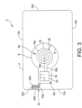
- FIGS. 2 and 3 illustrate the card core 2 of FIG. 1 having a plurality of circuit elements positioned within the cutout 8, in accordance with some embodiments.
- a first circuit element 16a such as an antenna 18, may be positioned within a first portion 8a of a cutout 8.
- the antenna 18 includes a plurality of concentric wire coils.
- the antenna 18 can include any suitable antenna, such as a printed antenna including one or more circular coils. Although a generally circular antenna is illustrated, it will be appreciated by those skilled in the art that the antenna 18 can have any suitable shape and/or any suitable number of windings (or coils).
- the first circuit element 16a can include a minimum thickness, such as, for example, a thickness between 50 and 100 microns, between 75 and 90 microns, and/or any other suitable thickness.
- the thickness of the first circuit element 16a may be less than, greater than, and/or equal to the thickness of the card core 2.
- the first circuit element 16a is positioned within the first cutout portion 8a such that a gap 26 is maintained between the edge 9 of the cutout 8 and the outer edge of the first circuit element 16a.
- the antenna 8 is positioned to ensure a gap 26 suitable gap, such as at least 300 microns, at least 500 microns, at least 700 microns, 300-900 microns, up to 1000 microns, up to 2000 microns, and/or any other suitable gap is maintained between an outer coil of the antenna 18 and the edge 9.
- the gap 26 can include any gap sufficient to electromagnetically isolate the first circuit element 16a from the material of the body 4.
- the gap 26 is selected based on one or more dimensions of the card core 2 and/or a credential card formed from the card core 2. For example, in some embodiments, the gap 26 is a distance equal to at least the width of a finished credential card formed using the card core 2.
- a finished credential card may have any thickness sufficient to contain the card core 2, one or more circuit elements positioned within the cutout 8, and/or any additional layers formed around the card core 2.
- a finished credential card may have a thickness of at least 700 microns, at least 750 microns, at least 800 microns, etc.
- the first circuit element 16a is coupled to a plurality of contact pads 24a, 24b positioned within the second cutout portion 8b of the cutout by a plurality of leads 28a, 28b.
- the contact pads 24a, 24b are sized and configured to couple a second circuit element 16b (see FIG. 3 ), positioned within the second cutout portion 8b, to the first circuit element 16a.
- the contact pads 24a, 24b are positioned within the second cutout portion 8b to allow the second circuit element 16b to be coupled to the contact pads 24a, 24b while maintaining at least a second predetermined gap 30 (see FIG. 3 ) between the edge 9 of the cutout 8 and the second circuit element 16b.
- the contact pads 24a, 24b are omitted and the second circuit element 16b may be directly coupled or not coupled to the first circuit element 16a.
- the first circuit element 16a, the contact pads 24a, 24b, and the leads 28a, 28b are formed integrally on a supporting film 17 (see FIG. 5 ).
- the supporting film 17 is sized and configured to be received within the cutout 8 while maintain the predetermined gaps 26, 30 between the circuit elements 16a, 16b and the edge 9 of the cutout 8.
- the first circuit element 16a, the contact pads 24a, 24b, and/or the leads 28a, 28b may be formed integrally on the supporting film 17 using any suitable formation method.
- the first circuit element 16a, the contact pads 24a, 24b and/or the leads 28a, 28b are printed circuit elements that are printed onto the supporting film 17 using a process to print conductive traces and/or other materials.
- FIG. 3 illustrates the card core 2 of FIG. 2 having a second circuit element 16b positioned within a second portion 8b of the cutout 8.
- the second circuit element 16b can include any suitable circuit element, such as, for example, an active circuit element(e.g., a direct contact System-on-Chip (SoC) element) 32.
- SoC System-on-Chip
- the second circuit element 16b may be positioned over and coupled to the contact pads 24a, 24b positioned within the second cutout 8b.
- the second circuit element 16b is electromagnetically isolated from the body 4 of the card core 2.
- the direct contact SoC element 32 is limited to direct contact coupling between the SoC element 32 and the antenna 18 and does not include any inductive coupling elements, effectively isolating the SoC element 32 from the material of the body 4.
- the second circuit element 16b may be positioned a predetermined distance from the edge 9 of the cutout 8 such that a second circuit element 16b capable of inductive, conductive, or other contactless coupling is effectively isolated from the material of the body 4.
- the contact pads 24a, 24b and the first circuit element 16a are maintained in a co-planar relationship (i.e., are parallel with respect to a plane defined by the body 4).
- a second circuit element 16b coupled to the contact pads 24a, 24b will be positioned out-of-plane (i.e., above or below) the first circuit element 16a.
- the second circuit element 16b is coupled to the first circuit element 16a only through the leads 28a, 28b and does not include any additional coupling (i.e., inductive, conductive, etc.) between the second circuit element 16b and the first circuit element 16a.
- the second circuit element 16b includes a second antenna (not shown).
- the second antenna can have a different configuration as compared to the antenna 16 (e.g., greater and/or lesser antenna area, larger/smaller material, different shape, etc.) such that the second antenna produce different responses as compared to the antenna 16 when each is simultaneously exposed to the same electromagnetic signal.
- the card core 2 and the plurality of circuit elements 16a, 16b positioned within the cutout 8 can be coupled between one or more additional layers, materials, and/or surfaces to form a credential core and/or a finished credential card (e.g., a credit/debit card, and ATM or bank card, an identification card, a state issued license or identification (e.g., driver's license), a security badge, a loyalty card, biometric card, etc.).
- the additional layers can include any suitable materials, such as, for example, metal, plastic, vinyl, and/or other materials.
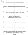
- FIG. 4 is a flowchart illustrating a method 100 of forming a credential card including a card core 2, in accordance with some embodiments.
- a card core 2 including a body 4 defining at least one cutout 8 is formed.
- the card core 2 can be formed using any suitable technique, such as, for example, pressing, stamping, milling, molding, etc.
- the body 4 is formed defining the cutout 8.
- a solid body is formed and the cutout 8 is subsequently formed in the solid body using any suitable technique, such as, for example, milling, drilling, etching, cutting, etc.
- a sinuous line discontinuity 10 is formed in the body 4 extending from a first edge 12a of the body 4 to the cutout 8.
- the sinuous line discontinuity 10 can be formed using any suitable technique, such as, for example, etching, stamping, laser cutting, mechanical cutting (milling or other mechanical/contact cutting), water-jet cutting, etc.
- the sinuous line discontinuity 10 includes one or more curves 34a, 34b and one or more straight line segments 36a-36c.
- the straight line segments 36a-36c are parallel and define a plurality of fingers 22a, 22b configured to provide a flex profile substantially similar to the flex profile of the body 4.
- a surface 5 of the body 4 may be treated to form one or more patterns and/or images on the surface.
- the surface of the body 4 may be etched, milled, and/or otherwise processed to form a predetermined pattern, images, pictures, symbols, trademarks, words, pictograms, or other visual indicators.
- at least a portion of the surface 5 may be colorized using any suitable colorization process, such as, for example, inking, printing, sintering, etc. The colorization may be in combination with and/or alternative to the formation of one or more patterns or images through surface treatment.
- steps 102-106 are illustrated as separate steps, it will be appreciated that steps 102-106 may be integrated into and/or performed simultaneously one or more of steps 102-106, and each combination is within the scope of this disclosure.
- one or more circuit elements are positioned within the cutout 8 defined in the card core 2.
- a first circuit element 16a, a plurality of contact pads 24a, 24b, and a plurality of leads 28a, 28b are formed on a circuit core using any suitable method.
- the first circuit element 16a, a plurality of contact pads 24a, 24b, and a plurality of leads 28a, 28b may include printed circuit elements formed on the circuit core.
- the circuit core is positioned within the cutout 8 such that a first gap 26 is defined between the first circuit element 16a and the edge 9 of the cutout 8 to effectively electromagnetically isolate the first circuit element 16a from the material of the body 4.
- the circuit core and/or the individual circuit elements may be positioned using any suitable method, such as, for example, by hand, by a pick-and-place method, and/or using any other suitable method.
- a second circuit element 16b may be positioned within the cutout 8, for example, within a second portion 8b of the cutout 8 simultaneous with the placement of the first circuit element 16a and/or the contact pads 24a, 24b.
- a credential core 200 including the card core 2 is formed.
- the credential core may be formed by coupling a thermoplastic layer 80 on a first side of the card core 2, as illustrated in FIG. 5 .
- the thermoplastic layer 80 may be simultaneously coupled to the card core 2 and/or the circuit elements 16a positioned therein so as to form a credential core 200.
- the thermoplastic layer 80 is coupled to the card core 2 at a predetermined pressure and/or at a predetermined temperature.
- the thermoplastic layer 80 may include any suitable material, such as, for example, a moly-based material (e.g., molybendum), polyvinyl chloride (PVC), a copolymer of vinyl chloride, polyolefin, polycarbonate, polyester, polyamide, acrylonitrile butadiene styrene copolymer (ABS), and the like.
- a moly-based material e.g., molybendum
- PVC polyvinyl chloride
- ABS acrylonitrile butadiene styrene copolymer
- a material layer 82 may be positioned between the thermoplastic layer 80 and the card core 2.
- the material layer 82 may include any suitable material, such as, for example, a cross-linkable polymer, an adhesive, and/or any other suitable material. Examples of cross-linkable polymers are disclosed in U.S. Patent 9,275,321, granted on March 1, 2016 , and entitled "Information Carrying Card Comprising a Cross-Linked Polymer Composition, and Method of Making the Same".
- a credential card may be formed by positioning one or more additional layers above and/or below the credential core formed at step 210.
- the additional layers may include any suitable materials or layers, such as, for example, image layers, sealing layers, thermoplastic layers, metal layers, conductive layers, non-conductive layers, and/or any other suitable layers.
- image layers such as, for example, image layers, sealing layers, thermoplastic layers, metal layers, conductive layers, non-conductive layers, and/or any other suitable layers.
- a credential card including a card core, such as a card core 2, disclosed herein can be formed using any suitable method.
- a credential card including a card core 2 may be formed using a cold laminate process, injection molding, milling, laser cutting, water-jet processes, etc.
- each layer positioned above the contact pads 24a, 24b may be removed to expose the contact pads and a second circuit element 16b may be coupled to the contact pads 24a, 24b.
- the contact pads 24a, 24b may be exposed using any suitable process, such as, for example, etching, drilling, milling, etc.
- a portion of the credential card or card core may be removed around the contact pads 24a, 24b sufficient to allow a second circuit element 16b, such as a direct contact SoC element 32, to be positioned with a surface parallel to a plane defined by a surface of the credential card and/or the card core (as illustrated in FIG. 3 ).
- FIG. 6 illustrates a card core 2a having a sinuous line discontinuity 10a including a first straight line segment 36a and a second straight line segment 36b defining a single flexible finger 22, in accordance with some embodiments.
- the card core 2a is similar to the card core 2 discussed above, and similar description is not repeated herein.
- the sinuous line discontinuity 10a generally defines a curved path (e.g., a notch or channel) extending from an inner edge of the cutout 8 to an outer edge 12a of the core card 2a
- FIG. 7 illustrates a card core 2b having a sinuous line discontinuity 10b including an extended straight line portion 42a and a truncated straight line portion 42b, in accordance with some embodiments.
- the card core 2b is similar to the metal card core 2 discussed above in conjunction with FIG. 5 , and similar description is not repeated herein.
- the card core 2b includes a sinuous line discontinuity 10b coupled to a lower portion of the second portion 8b of the cutout 8.
- a first substantially straight portion 42a of the discontinuity 10b has a longer length as compared to a first substantially straight portion 36a of the sinuous line discontinuity 10a of the card core 2 and a second straight portion 42b has a substantially shorter length.
- the sinuous line discontinuity 10b further includes a first portion 38a extending from the cutout 8 and a second portion 38b extending from the first edge 12a, each disposed at a non-parallel and non-perpendicular angle with respect to each of the edges 12a, 12b, 14a, 14b of the card core 2b.
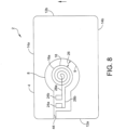
- FIG. 8 illustrates an object that is not part of the invention, namely a card core 2c including a straight line discontinuity 44.
- the card core 2c is similar to the card cores 2-2b described above, and similar description is not repeated herein.
- the card core 2c replaces the sinuous line discontinuity 10 with a straight line discontinuity 44 extending from an edge 9 of the cutout 8 to an edge 12a of the card core 2c.
- the straight line discontinuity 44 includes a thickness selected to effectively isolate a first side 20a of the discontinuity 44 from a second side 20b without substantially weakening the structure of the card core 2.
- the straight line discontinuity 44 includes a width (e.g., distance from first side 20a to second side 20b) of at least 300 microns, at least 500 microns, at least 700 microns, 300-900 microns, and/or any other suitable width.
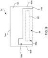
- FIG. 9 illustrates an object that is not part of the invention, namely a card core 2d including a cutout 58 extending to an edge 14a of the card core 2d.
- the card core 2d is substantially similar to the card core 2 described above, and similar description is not repeated herein.
- the card core 2d includes a body 52 defining a cutout 58 including a first portion 58a and a second portion 58b.
- the body 52 extends substantially defined by a first short edge 12a, a second short edge 12b, a first long edge 14a, and a second long edge 14b.
- the cutout 58 extends from the first long edge 14a into the body 52 such that the cutout 58 defines a portion of the first long edge 14a of the card.
- one or more circuit elements may be positioned within any portion of the cutout 58 such that a gap (see FIGS. 2-3 ) sufficient to electrically isolate the circuit element from the card core 2d is maintained.
- the cutout 58 includes a first portion 58a having a first rectangular geometry extending between a first edge portion 60a of the card core 2d and a second edge portion 60b and a second portion 58b having a second rectangular geometry continuous with the first portion 58a.
- the cutout 58 can include any number of portions defining any number of geometries, and such embodiments are within the scope of this disclosure.
- a portion of the cutout 58 defines an embossable area 62.
- the embossable area 62 includes a portion of a card core 2d and/or a finished credential card including the card core 2d that may be subjected to known embossing techniques.
- FIG. 10 illustrates a finished credential card 70 (i.e., a credit card) including an overlay layer 72 and an embossing 74 disposed within the embossable area 62.
- FIG. 10 further illustrates a circuit element 76, such as a direct contact SoC element, disposed within the second portion 58b of the cutout 58.
- the finished credential card 70 may be formed using any known technique, such as, for example, the method 100 discussed above in conjunction with FIG. 4 .
Landscapes
- Engineering & Computer Science (AREA)
- Physics & Mathematics (AREA)
- Computer Hardware Design (AREA)
- Microelectronics & Electronic Packaging (AREA)
- General Physics & Mathematics (AREA)
- Theoretical Computer Science (AREA)
- Electromagnetism (AREA)
- Credit Cards Or The Like (AREA)
Claims (15)
- Noyau de carte métallique (2 ; 2a ; 2b) destiné à être utilisé dans une carte de créance, comprenant :un corps (4) composé d'un matériau métallique, le corps définissant :une découpe (8) qui comprend une ouverture dans le corps, etune discontinuité (10 ; 10a ; 10b) qui comprend un canal défini par le corps et s'étendant d'une surface extérieure (12a, 12b, 14a, 14b) du corps à la découpe ; etau moins un élément de circuit (16a, 16b) positionné à l'intérieur de la découpe (8),caractérisé par le fait que la discontinuité comprend une ligne sinueuse (10 ; 10a ; 10b) qui comprend au moins une partie courbe (34a-34d) et au moins une partie droite (36a-36c ; 42a, 42b),et en ce que la découpe (8) définit une taille et une géométrie telles qu'un espace (26) entre l'au moins un élément de circuit (16a, 16b) et un bord (9) de la découpe présente un espacement efficace pour isoler électromagnétiquement l'au moins un élément de circuit (16a, 16b) du matériau métallique du corps (4).
- Noyau de carte métallique selon la revendication 1, dans lequel la discontinuité de ligne sinueuse (10) définit une pluralité de doigts flexibles (22a, 22b) configurés pour fournir un profil de flexion similaire à une partie continue du corps (4) lorsqu'une force est appliquée au noyau de carte métallique (2).
- Noyau de carte métallique selon la revendication 1, dans lequel la discontinuité de ligne sinueuse (10a ; 10b) comprend un premier segment de ligne droite (36a) et un second segment de ligne droite (36b) définissant un unique doigt flexible (22).
- Noyau de carte métallique selon la revendication 1, dans lequel l'au moins une partie incurvée (34a-34d) définit une courbe de 180°.
- Noyau de carte métallique selon la revendication 4, dans lequel la discontinuité de ligne sinueuse (10 ; 10a; 10b) définit une courbe oscillante répétitive lisse.
- Noyau de carte métallique selon la revendication 1, dans lequel la découpe (8) comprend une première partie (8a) dotée d'une première géométrie définie par le bord (9) de la découpe et une deuxième partie (8b) dotée d'une deuxième géométrie définie par le bord de la découpe, et dans lequel la première et la deuxième partie (8a, 8b) de la découpe (8) se chevauchent de telle sorte que la première partie est continue avec la deuxième partie.
- Noyau de carte métallique selon la revendication 6, dans lequel la première géométrie est circulaire et la seconde géométrie est carrée.
- Noyau de carte métallique selon la revendication 6, dans lequel un premier élément de circuit (16a) est positionné dans la première partie (8a) de la découpe (8) et un second élément de circuit (16b) est positionné dans la seconde partie (8b) de la découpe.
- Noyau de carte métallique selon la revendication 8, dans lequel le premier élément de circuit (16a) est couplé à une pluralité de plots de contact (24a, 24b) positionnés dans la seconde partie (8b) de la découpe (8), et dans lequel le second élément de circuit (16b) est couplé au premier élément de circuit (16a) par les plots de contact (24a, 24b).
- Noyau de carte métallique selon la revendication 9, dans lequel le premier élément de circuit (16a) est une antenne et le second élément de circuit (16b) est un élément de système sur puce (SoC) à contact direct.
- Noyau de carte métallique selon la revendication 1, dans lequel le corps (4) comprend un matériau non métallique conducteur.
- Carte de créance comprenant :un noyau de carte métallique (2 ; 2a ; 2b) selon l'une quelconque des revendications 1 à 11 ;une première couche de matériau (80, 82) disposée sur une première face du noyau de la carte métallique ; etune seconde couche de matériau disposée sur une seconde face du noyau de la carte métallique, dans laquelle la première couche de matériau et la seconde couche de matériau sont chacune couplées au corps (4) du noyau de la carte métallique dans une première région de la carte de créance, dans laquelle la première couche de matériau est couplée à la seconde couche de matériau dans une seconde région de la carte de créance, et dans laquelle la seconde région est sensiblement alignée sur la découpe (8) du noyau de la carte métallique.
- Carte de créance selon la revendication 12, dans laquelle la discontinuité de la ligne sinueuse (10 ; 10a ; 10b) définit une pluralité de doigts flexibles (22a, 22b) configurés pour distribuer une pression de couple afin de fournir un profil de flexion similaire au reste de la carte de créance, incorporant des sections solides du corps (4), afin d'éviter la fissuration ou la rupture de toute couche de la carte de créance lorsqu'une pression de flexion est appliquée à ladite carte de créance.
- Noyau de carte métallique selon la revendication 12, dans lequel la découpe (8) comprend une première partie (8a) dotée d'une première géométrie définie par le bord et une deuxième partie (8b) dotée d'une deuxième géométrie définie par le bord, dans lequel la première et la deuxième partie (8a, 8b) de la découpe (8) se chevauchent de telle sorte que la première partie est continue avec la deuxième partie, et dans lequel la seconde région est sensiblement alignée avec la première et la deuxième parties (8a, 8b) de la découpe (8).
- Procédé de formation d'une carte de créance, comprenant :la formation d'une découpe (8) dans un corps (4) d'un noyau de carte métallique (2 ; 2a ; 2b), dans lequel le corps comprend un matériau métallique, et dans lequel la découpe comprend une ouverture dans le corps ;la formation d'une discontinuité de ligne sinueuse (10 ; 10a ; 10b) dans le corps, dans lequel la discontinuité de ligne sinueuse comprend un canal défini par le corps et s'étendant d'une surface extérieure (12a, 12b, 14a, 14b) du corps à la découpe, et dans lequel la discontinuité de ligne sinueuse comprend au moins une partie incurvée (34a-34d) et au moins une partie droite (36a-36c ; 42a, 42b) ;le positionnement d'au moins un élément de circuit (16a, 16b) dans la découpe, dans lequel la découpe définit une taille et une géométrie telles qu'un espace (26) entre l'au moins un élément de circuit et un bord (9) de la découpe présente un espacement efficace pour isoler électromagnétiquement l'au moins un élément de circuit du matériau métallique du corps ;le positionnement d'une couche de matériau thermoplastique (80, 82) sur une première face du noyau de la carte métallique ; etle couplage de la couche de matériau thermoplastique au corps du noyau de la carte dans une première région et de la couche de matériau thermoplastique à l'au moins un élément de circuit dans une seconde région, la seconde région étant sensiblement alignée sur la découpe.
Applications Claiming Priority (2)
| Application Number | Priority Date | Filing Date | Title |
|---|---|---|---|
| US201862639535P | 2018-03-07 | 2018-03-07 | |
| PCT/US2019/020919 WO2019173455A1 (fr) | 2018-03-07 | 2019-03-06 | Carte métallique |
Publications (3)
| Publication Number | Publication Date |
|---|---|
| EP3762871A1 EP3762871A1 (fr) | 2021-01-13 |
| EP3762871A4 EP3762871A4 (fr) | 2021-11-10 |
| EP3762871B1 true EP3762871B1 (fr) | 2024-08-07 |
Family
ID=67846808
Family Applications (1)
| Application Number | Title | Priority Date | Filing Date |
|---|---|---|---|
| EP19763342.3A Active EP3762871B1 (fr) | 2018-03-07 | 2019-03-06 | Carte métallique |
Country Status (4)
| Country | Link |
|---|---|
| US (5) | US11361204B2 (fr) |
| EP (1) | EP3762871B1 (fr) |
| CN (1) | CN111819577B (fr) |
| WO (1) | WO2019173455A1 (fr) |
Families Citing this family (14)
| Publication number | Priority date | Publication date | Assignee | Title |
|---|---|---|---|---|
| US11347993B2 (en) | 2019-08-12 | 2022-05-31 | Federal Card Services, LLC | Dual interface metal cards and methods of manufacturing |
| US12277462B2 (en) | 2019-08-14 | 2025-04-15 | Federal Card Services, LLC | Metal-containing dual interface smartcards |
| US11113593B2 (en) | 2019-08-15 | 2021-09-07 | Federal Card Services; LLC | Contactless metal cards with fingerprint sensor and display |
| US11416728B2 (en) | 2019-08-15 | 2022-08-16 | Federal Card Services, LLC | Durable dual interface metal transaction cards |
| US11455507B2 (en) | 2019-10-13 | 2022-09-27 | Federal Card Services, LLC | Metal transaction cards containing ceramic having selected coloring and texture |
| WO2021097208A1 (fr) * | 2019-11-16 | 2021-05-20 | Federal Card Services, LLC | Carte métallique de transactions activées par rfid dotée d'une ouverture façonnée et d'une fente façonnée |
| US11341385B2 (en) | 2019-11-16 | 2022-05-24 | Federal Card Services, LLC | RFID enabled metal transaction card with shaped opening and shaped slit |
| FR3105856B1 (fr) * | 2019-12-31 | 2022-05-06 | Idemia France | Carte à puce métallique apte à fonctionner en sans contact |
| USD1032613S1 (en) | 2020-02-02 | 2024-06-25 | Federal Card Services, LLC | Smart card |
| EP4002210A1 (fr) | 2020-11-12 | 2022-05-25 | AdvanIDe Holdings Pte. Ltd. | Incrustation de carte pour connexion directe ou technologie de couplage inductif |
| US11551050B2 (en) | 2020-11-12 | 2023-01-10 | Advanide Holdings Pte. Ltd. | Card inlay for direct connection or inductive coupling technology |
| US12159180B1 (en) | 2021-11-29 | 2024-12-03 | Metaland Llc | RFID enabled metal transaction cards with coupler coil couplings and related methods |
| WO2024128418A1 (fr) * | 2022-12-15 | 2024-06-20 | (주)바이오스마트 | Carte métallique ayant un corps en verre, et son procédé de fabrication |
| US12430531B2 (en) * | 2023-01-03 | 2025-09-30 | Giesecke+Devrient ePayments GmbH | Method of manufacturing a card-shaped data carrier and lamination plate therefor |
Family Cites Families (301)
| Publication number | Priority date | Publication date | Assignee | Title |
|---|---|---|---|---|
| US2890202A (en) | 1953-07-20 | 1959-06-09 | Pittsburgh Plate Glass Co | Method of preparing acrylate esters of epoxy resins |
| US3024216A (en) | 1958-07-28 | 1962-03-06 | Union Carbide Corp | Compositions of partially hydrolyzed vinyl chloride-vinyl acetate copolymers and polyurethane resins, polyethylene coated with same and process for making coated article |
| US3191788A (en) | 1963-03-26 | 1965-06-29 | Grand Specialties Company | Load tilting mechanism for industrial truck |
| US3847654A (en) | 1970-06-08 | 1974-11-12 | M & T Chemicals Inc | Substrate bonded with vinyl dispersion textured coating |
| JPS5271590A (en) | 1975-12-01 | 1977-06-15 | Bridgestone Corp | Production of novel high polymer |
| US4115479A (en) | 1976-08-11 | 1978-09-19 | Vynacron Dental Co. | Casting resins by polymerizing liquid monomer in mixture of particulated vinyl halide resins |
| DE2837435B2 (de) | 1978-08-28 | 1981-06-25 | Friedrich Horst 5840 Schwerte Papenmeier | Verfahren und Vorrichtung zum Aufbereiten von PVC-Pulver |
| DE2920012C2 (de) * | 1979-05-17 | 1988-09-29 | GAO Gesellschaft für Automation und Organisation mbH, 8000 München | Ausweiskarte mit IC-Baustein und Verfahren zur Herstellung einer derartigen Ausweiskarte |
| US4310451A (en) | 1979-10-25 | 1982-01-12 | Diamond Shamrock Plastics Corporation | Free flowing rigid PVC resin powder compositions |
| DE3153769C2 (de) * | 1981-04-14 | 1995-10-26 | Gao Ges Automation Org | Trägerelement zum Einbau in Ausweiskarten |
| US4382201A (en) | 1981-04-27 | 1983-05-03 | General Electric Company | Ultrasonic transducer and process to obtain high acoustic attenuation in the backing |
| US4480079A (en) | 1982-04-12 | 1984-10-30 | Imperial Chemical Industries Plc | Copolymerization of unsaturated urethane monomers |
| US4399061A (en) | 1981-10-14 | 1983-08-16 | Rca Corporation | Preparation of video disc molding composition |
| DE3248385A1 (de) | 1982-12-28 | 1984-06-28 | GAO Gesellschaft für Automation und Organisation mbH, 8000 München | Ausweiskarte mit integriertem schaltkreis |
| US4463128A (en) | 1983-05-09 | 1984-07-31 | W. R. Grace & Co. | Reactive plastisol dispersion |
| JPS60252992A (ja) | 1984-05-30 | 1985-12-13 | Toshiba Corp | Icカ−ド |
| FR2570101B1 (fr) | 1984-09-07 | 1987-09-25 | Sotimag | Procede antifraude pour document de valeur |
| DE3575965D1 (de) | 1984-12-19 | 1990-03-15 | Soil Machine Dynamics Ltd | Verfahren und vorrichtung zum ausheben von boden. |
| DE3685033D1 (de) | 1985-01-25 | 1992-06-04 | Ici Plc | Polymerisierbare urethanzusammensetzungen. |
| DE8504263U1 (de) | 1985-02-15 | 1986-06-12 | Schwan-Stabilo Schwanhäußer GmbH & Co, 8500 Nürnberg | Pudermine für Kosmetikstifte |
| DE3519053A1 (de) | 1985-05-28 | 1986-12-18 | W.R. Grace & Co., Cambridge, Mass. | Dichtungsmasse |
| JPH0686177B2 (ja) | 1986-09-29 | 1994-11-02 | 河西工業株式会社 | 自動車用内装部品 |
| GB8624082D0 (en) | 1986-10-08 | 1986-11-12 | Dunlop Cct Sa | Vinyl chloride polymer products |
| JPS63141790A (ja) * | 1986-12-03 | 1988-06-14 | 菱電化成株式会社 | 識別カ−ド |
| JPS63185630A (ja) | 1987-01-29 | 1988-08-01 | 東洋鋼板株式会社 | 高硬度塩化ビニル被覆鋼板の製造方法 |
| US4742085A (en) | 1987-04-14 | 1988-05-03 | The B. F. Goodrich Company | Crosslinked porous skinless particles of PVC resin and process for producing same |
| US4775701A (en) | 1987-04-14 | 1988-10-04 | The B. F. Goodrich Company | Mass process for producing porous friable particles of crosslinked PVC resin |
| US4775702A (en) | 1987-04-14 | 1988-10-04 | The B. F. Goodrich Company | Inversion process for producing low-skin porous friable particles of crosslinked PVC resin |
| US4775700A (en) | 1987-04-14 | 1988-10-04 | The B. F. Goodrich Company | Process for producing porous skinless particles of crosslinked PVC resin |
| US4775698A (en) | 1987-04-14 | 1988-10-04 | The B. F. Goodrich Company | Process for producing porous substantially skinless particles of crosslinked PVC resin |
| US4775699A (en) | 1987-04-14 | 1988-10-04 | The B. F. Goodrich Company | Crosslinked porous skinless particles of PVC resin |
| KR900702481A (ko) | 1988-06-21 | 1990-12-07 | 원본미기재 | 휴대용 전자 토큰 제조방법 |
| KR970005475B1 (ko) | 1988-07-15 | 1997-04-16 | 클레리언트 파이넌스(비브이아이) 리미티드 | 폴리-[α-히드록시-(아크릴,크로톤,또는 아크릴+크로톤)산]의 폴리락톤류 및 상응하는 염류의 제조방법 |
| US5084501A (en) | 1988-11-07 | 1992-01-28 | Armstrong World Industries, Inc. | Highly filled resin powder |
| US5324506A (en) | 1988-11-23 | 1994-06-28 | Estee Lauder, Inc. | Colored cosmetic compositions |
| US5143723A (en) | 1988-11-23 | 1992-09-01 | Estee Lauder, Inc. | Colored cosmetic compositions |
| US4954195A (en) | 1989-02-13 | 1990-09-04 | Lockheed Corporation | Production of thermoset composites containing thermoplastic fillers |
| US5084699A (en) | 1989-05-26 | 1992-01-28 | Trovan Limited | Impedance matching coil assembly for an inductively coupled transponder |
| EP0441047B1 (fr) | 1990-01-19 | 1996-06-05 | Minnesota Mining And Manufacturing Company | Composition thermodurcissable |
| JPH03239595A (ja) | 1990-02-16 | 1991-10-25 | Dainippon Printing Co Ltd | カード製造方法 |
| NL9000840A (nl) | 1990-04-10 | 1991-11-01 | Wavin Bv | Werkwijze en installatie voor het vervaardigen van kunststofvoortbrengsels met behulp van een warm mengsel van pvc-poeder en additieven, alsmede een voor toepassing bij deze werkwijze geschikte warmmenger. |
| US5198501A (en) | 1990-08-20 | 1993-03-30 | Air Products And Chemicals, Inc. | In-situ polymerized blends of vinyl acetate/ethylene copolymar and poly(vinyl chloride) |
| JPH04216850A (ja) | 1990-12-17 | 1992-08-06 | Nippon Zeon Co Ltd | 塩化ビニル系プラスチゾル組成物 |
| USD341092S (en) | 1991-04-08 | 1993-11-09 | Manufacture Jaeger-Le Coultre, S.A. | Wrist watch |
| US5281855A (en) | 1991-06-05 | 1994-01-25 | Trovan Limited | Integrated circuit device including means for facilitating connection of antenna lead wires to an integrated circuit die |
| DE4135937C2 (de) | 1991-10-31 | 1997-07-03 | Pegulan Tarkett Ag | Verfahren zu Herstellen von Latex-, PVC-, und Weichmacher-freien Textil- oder Kunststoff-Boden- und Wandbelägen |
| US5233022A (en) | 1991-08-26 | 1993-08-03 | United Technologies Automotive, Inc. | Flow property shelf life of PVC dry blend powders |
| US5198170A (en) | 1991-09-19 | 1993-03-30 | The B. F. Goodrich Company | Method for extrusion of powered PVC compounds |
| JP3049894B2 (ja) | 1991-11-27 | 2000-06-05 | 日本ゼオン株式会社 | アクリル酸エステル系共重合体プラスチゾル組成物 |
| US5255430A (en) | 1992-10-08 | 1993-10-26 | Atmel Corporation | Method of assembling a module for a smart card |
| FR2701268B1 (fr) | 1993-02-05 | 1995-04-14 | Atochem Elf Sa | Peintures à base de poudres de polyamide destinées au revêtement de profilés PVC. |
| US5407893A (en) | 1993-08-19 | 1995-04-18 | Konica Corporation | Material for making identification cards |
| JPH0793817A (ja) | 1993-09-24 | 1995-04-07 | Canon Inc | 情報記録媒体 |
| FR2713648B1 (fr) | 1993-12-15 | 1996-03-01 | Rhone Poulenc Chimie | Composition stabilisante pour polymère chloré comportant des béta-dicétones. |
| FR2716555B1 (fr) | 1994-02-24 | 1996-05-15 | Gemplus Card Int | Procédé de fabrication d'une carte sans contact. |
| DE69530922T2 (de) | 1994-03-31 | 2003-12-24 | Ibiden Co. Ltd., Ogaki | Vorrichtung mit elektronischem bauteil |
| JPH0817288A (ja) | 1994-07-04 | 1996-01-19 | Matsushita Electric Ind Co Ltd | 透明タッチパネル |
| FR2724477B1 (fr) | 1994-09-13 | 1997-01-10 | Gemplus Card Int | Procede de fabrication de cartes sans contact |
| US5975420A (en) | 1995-04-13 | 1999-11-02 | Dai Nippon Printing Co., Ltd. | Apparatus and method of manufacturing an integrated circuit (IC) card with a protective IC module |
| USD378064S (en) | 1995-05-11 | 1997-02-18 | Manufacture Jaeger-Le Coultre Sa | Wristwatch |
| US6611199B1 (en) | 1995-10-11 | 2003-08-26 | Motorola, Inc. | Capacitively powered portable communication device and associated exciter/reader and related method |
| CA2245775C (fr) | 1996-02-12 | 2004-04-06 | David Finn | Procede et dispositif pour la connexion d'un conducteur electrique |
| DE59701709C5 (de) | 1996-02-12 | 2014-01-09 | Smartrac Ip B.V. | Verfahren und vorrichtung zur kontaktierung eines drahtleiters |
| FR2761497B1 (fr) | 1997-03-27 | 1999-06-18 | Gemplus Card Int | Procede de fabrication d'une carte a puce ou analogue |
| FR2762115B1 (fr) | 1997-04-10 | 1999-12-03 | Schlumberger Ind Sa | Procede d'insertion d'un module electronique dans un corps de carte a memoire electronique |
| US5955021A (en) | 1997-05-19 | 1999-09-21 | Cardxx, Llc | Method of making smart cards |
| NO310365B1 (no) | 1997-07-18 | 2001-06-25 | Norsk Hydro As | PVC-blanding, anvendelse av denne og metode for dens fremstilling |
| US6052062A (en) | 1997-08-20 | 2000-04-18 | Micron Technology, Inc. | Cards, communication devices, and methods of forming and encoding visibly perceptible information on the same |
| FR2769110B1 (fr) | 1997-09-26 | 1999-12-03 | Gemplus Card Int | Procede de fabrication d'un module ou etiquette electronique, module ou etiquette obtenue et support comportant un tel module ou etiquette |
| US6037879A (en) | 1997-10-02 | 2000-03-14 | Micron Technology, Inc. | Wireless identification device, RFID device, and method of manufacturing wireless identification device |
| US7012504B2 (en) | 2002-04-01 | 2006-03-14 | Micron Technology, Inc. | Wireless identification device, RFID device with push-on/push off switch, and method of manufacturing wireless identification device |
| US6768415B1 (en) | 1997-10-03 | 2004-07-27 | Micron Technology, Inc. | Wireless identification device, RFID device with push-on/push-off switch, method of manufacturing wireless identification device |
| WO1999026195A1 (fr) | 1997-11-14 | 1999-05-27 | Toppan Printing Co., Ltd. | Module ci composite et carte ci composite |
| USD404319S (en) | 1997-12-24 | 1999-01-19 | Manufacture Jaeger-Le Coultre Sa | Wristwatch |
| HU224551B1 (hu) | 1998-02-17 | 2005-10-28 | E.I.Du Pont De Nemours And Company, Inc. | Eljárás porbevonatok előállítására |
| US6241153B1 (en) | 1998-03-17 | 2001-06-05 | Cardxx, Inc. | Method for making tamper-preventing, contact-type, smart cards |
| US6353242B1 (en) | 1998-03-30 | 2002-03-05 | Kabushiki Kaisha Toshiba | Nonvolatile semiconductor memory |
| US6191382B1 (en) | 1998-04-02 | 2001-02-20 | Avery Dennison Corporation | Dynamic laser cutting apparatus |
| US6018299A (en) | 1998-06-09 | 2000-01-25 | Motorola, Inc. | Radio frequency identification tag having a printed antenna and method |
| US6107920A (en) | 1998-06-09 | 2000-08-22 | Motorola, Inc. | Radio frequency identification tag having an article integrated antenna |
| FR2779851B1 (fr) | 1998-06-12 | 2002-11-29 | Gemplus Card Int | Procede de fabrication d'une carte a circuit integre et carte obtenue |
| JP4689825B2 (ja) | 1998-08-26 | 2011-05-25 | センサーズ・フォー・メデセン・アンド・サイエンス・インコーポレーテッド | 光学式検知装置 |
| US6147605A (en) | 1998-09-11 | 2000-11-14 | Motorola, Inc. | Method and apparatus for an optimized circuit for an electrostatic radio frequency identification tag |
| DE69938929D1 (de) | 1998-09-11 | 2008-07-31 | Motorola Inc | Rfid-etikettenvorrichtung und verfahren |
| US6100804A (en) | 1998-10-29 | 2000-08-08 | Intecmec Ip Corp. | Radio frequency identification system |
| JP2000148959A (ja) | 1998-11-13 | 2000-05-30 | Henkel Japan Ltd | Icカードの製造法 |
| DE19855125A1 (de) | 1998-11-30 | 2000-05-31 | Basf Coatings Ag | Aus mindestens drei Komponenten bestehendes Beschichtungsmittel, Verfahren zu seiner Herstellung sowie seine Verwendung |
| DE19855146A1 (de) | 1998-11-30 | 2000-05-31 | Basf Coatings Ag | Aus mindestens drei Komponenten bestehendes Beschichtungsmittel, Verfahren zu seiner Herstellung sowie seine Verwendung |
| DE19855167A1 (de) | 1998-11-30 | 2000-05-31 | Basf Coatings Ag | Aus mindestens drei Komponenten bestehendes Beschichtungsmittel, Verfahren zu seiner Herstellung sowie seine Verwendung |
| US6730734B1 (en) | 1998-12-08 | 2004-05-04 | Rohm And Haas Company | Impact modifier compositions which enhance the impact strength properties and lower the viscosity of melt processed plastics resins and methods of making said compositions |
| SE521714C2 (sv) | 1999-01-20 | 2003-12-02 | Bozena Olsson | Nagellacksbortagande medel |
| US8636648B2 (en) | 1999-03-01 | 2014-01-28 | West View Research, Llc | Endoscopic smart probe |
| DE19915765C2 (de) | 1999-04-08 | 2001-06-21 | Cubit Electronics Gmbh | Kontaktloser Transponder und Verfahren zu seiner Herstellung |
| USD423374S (en) | 1999-04-21 | 2000-04-25 | Manufacture Jaeger-Le Coultre Sa | Wristwatch |
| US6376769B1 (en) | 1999-05-18 | 2002-04-23 | Amerasia International Technology, Inc. | High-density electronic package, and method for making same |
| FR2794266B1 (fr) | 1999-05-25 | 2002-01-25 | Gemplus Card Int | Procede de fabrication de dispositif electronique portable a circuit integre comportant un dielectrique bas cout |
| AU7084300A (en) | 1999-08-27 | 2001-03-26 | Cohesion Technologies, Inc. | Compositions that form interpenetrating polymer networks for use as high strength medical sealants |
| US8066190B2 (en) | 1999-09-07 | 2011-11-29 | American Express Travel Related Services Company, Inc. | Transaction card |
| US7093767B2 (en) | 1999-09-07 | 2006-08-22 | American Express Travel Related Services Company, Inc. | System and method for manufacturing a punch-out RFID transaction device |
| US7837116B2 (en) | 1999-09-07 | 2010-11-23 | American Express Travel Related Services Company, Inc. | Transaction card |
| US6764014B2 (en) | 1999-09-07 | 2004-07-20 | American Express Travel Related Services Company, Inc. | Transaction card |
| US7306158B2 (en) | 2001-07-10 | 2007-12-11 | American Express Travel Related Services Company, Inc. | Clear contactless card |
| US6581839B1 (en) | 1999-09-07 | 2003-06-24 | American Express Travel Related Services Company, Inc. | Transaction card |
| US6749123B2 (en) | 1999-09-07 | 2004-06-15 | American Express Travel Related Services Company, Inc. | Transaction card |
| NL1013028C2 (nl) | 1999-09-10 | 2001-03-13 | Dsm Nv | Informatiedragend vormdeel. |
| US6784230B1 (en) | 1999-09-23 | 2004-08-31 | Rohm And Haas Company | Chlorinated vinyl resin/cellulosic blends: compositions, processes, composites, and articles therefrom |
| US6296188B1 (en) | 1999-10-01 | 2001-10-02 | Perfect Plastic Printing Corporation | Transparent/translucent financial transaction card including an infrared light filter |
| DE19947521A1 (de) | 1999-10-02 | 2001-04-05 | Basf Coatings Ag | Mit aktinischer Strahlung aktivierbare Bindungen enthaltendes festes Stoffgemisch und seine Verwendung |
| ES2280244T3 (es) | 1999-12-03 | 2007-09-16 | China Petro-Chemical Corporation | Caucho en polvo totalmente vulcanizado con diametro de particula controlable, procedimiento de preparacion y uso del mismo. |
| US7592394B2 (en) | 1999-12-15 | 2009-09-22 | Arkema France | Plastic compositions having mineral-like appearance |
| EP1111001B1 (fr) | 1999-12-23 | 2006-06-14 | Rohm And Haas Company | Additives pour plastics, la préparation et les mélanges |
| DE10014399A1 (de) | 2000-03-23 | 2001-10-04 | Wacker Polymer Systems Gmbh | Vernetzbare Polymerzusammensetzung |
| US6805998B2 (en) | 2000-03-24 | 2004-10-19 | Cymbet Corporation | Method and apparatus for integrated-battery devices |
| US6611050B1 (en) | 2000-03-30 | 2003-08-26 | International Business Machines Corporation | Chip edge interconnect apparatus and method |
| ITMI20010807A1 (it) | 2000-04-14 | 2002-10-13 | Saint Gobain | Procedimento per la fabbricazione di piste elettroconduttorici sunun substrato trasparente e substrato ottenuto |
| US7893435B2 (en) | 2000-04-18 | 2011-02-22 | E Ink Corporation | Flexible electronic circuits and displays including a backplane comprising a patterned metal foil having a plurality of apertures extending therethrough |
| JP2002033296A (ja) | 2000-04-26 | 2002-01-31 | Lintec Corp | シリコンウエハ用の補強材および該補強材を用いたicチップの製造方法 |
| EP1158601A1 (fr) | 2000-05-15 | 2001-11-28 | Häni Prolectron Ag | Dispositif de support avec antenne à sensibilité réduite |
| US6380272B1 (en) | 2000-08-23 | 2002-04-30 | Kuei Yung Wang Chen | Manufacturing method for structural members from foamed plastic composites containing wood flour |
| US6477926B1 (en) | 2000-09-15 | 2002-11-12 | Ppg Industries Ohio, Inc. | Polishing pad |
| JP2004517980A (ja) | 2000-09-21 | 2004-06-17 | ローム アンド ハース カンパニー | 極性モノマーと多価カチオンとに関わる方法および組成物 |
| US6599993B1 (en) | 2000-10-11 | 2003-07-29 | Basf Corporation | Low gloss textured powder coating |
| US6634564B2 (en) | 2000-10-24 | 2003-10-21 | Dai Nippon Printing Co., Ltd. | Contact/noncontact type data carrier module |
| US20020091178A1 (en) | 2001-01-05 | 2002-07-11 | Hossein Amin-Javaheri | Polyvinyl chloride composition |
| US20020119294A1 (en) | 2001-02-28 | 2002-08-29 | Jason Monkarsh | Light-emitting, light-rechargeable labels for containers |
| JP3916405B2 (ja) | 2001-03-06 | 2007-05-16 | 松下電器産業株式会社 | 電子部品実装済部品の製造方法、電子部品実装済完成品の製造方法、及び半導体部品実装済完成品 |
| US6551537B2 (en) | 2001-03-08 | 2003-04-22 | Nan Ya Plastics Corporation | Manufacturing method for structural members from foamed plastic composites containing wood flour |
| US20020125431A1 (en) | 2001-03-12 | 2002-09-12 | Peter Hwang | Infrared radiation detection device |
| US6462273B1 (en) | 2001-03-16 | 2002-10-08 | Micron Technology, Inc. | Semiconductor card and method of fabrication |
| US20020132086A1 (en) | 2001-03-19 | 2002-09-19 | Hsu Tang Su-Tuan | Sweat-absorbing and non-slip pad |
| FR2824939B1 (fr) | 2001-05-16 | 2003-10-10 | A S K | Procede de fabrication d'une carte a puce sans contact a l'aide de papier transfert et carte a puce obtenue a partir de ce procede |
| US6790893B2 (en) | 2001-11-30 | 2004-09-14 | Pyrophobic Systems Ltd. | Compound of intumescent powder and thermoplastic material |
| US7097549B2 (en) | 2001-12-20 | 2006-08-29 | Ppg Industries Ohio, Inc. | Polishing pad |
| DE10163825A1 (de) | 2001-12-22 | 2003-07-03 | Degussa | Pulverlackzusammensetzungen aus kristallinen Urethanacrylaten und deren Verwendung |
| US6639309B2 (en) | 2002-03-28 | 2003-10-28 | Sandisk Corporation | Memory package with a controller on one side of a printed circuit board and memory on another side of the circuit board |
| US7112625B2 (en) | 2002-03-29 | 2006-09-26 | Sanyo Chemical Industries, Ltd. | Thermocrosslinkable resin dispersion |
| US20040002559A1 (en) | 2002-04-10 | 2004-01-01 | Malisa Troutman | Flame retardant coatings |
| EP1502763A4 (fr) | 2002-04-23 | 2008-03-26 | Ricoh Kk | Carte d'enregistrement/affichage de donnees, procede de traitement d'image utilisant celle-ci et processeur d'image |
| US20030216701A1 (en) | 2002-05-15 | 2003-11-20 | Gentho Sumarta | Synthetic glove and process for making |
| FR2840459B1 (fr) | 2002-05-28 | 2004-07-16 | Itt Mfg Enterprises Inc | Connecteur electrique pour une carte a puce comportant un commutateur perfectionne |
| US6918984B2 (en) | 2002-06-24 | 2005-07-19 | Loctite (R&D) Limited | Photocurable adhesive compositions, reaction products of which have low halide ion content |
| US6786415B2 (en) | 2002-08-06 | 2004-09-07 | Jung-Hua Yiu | Memory card connector |
| JP3866178B2 (ja) | 2002-10-08 | 2007-01-10 | 株式会社ルネサステクノロジ | Icカード |
| US6861475B2 (en) | 2002-10-16 | 2005-03-01 | Rohm And Haas Company | Smooth, flexible powder coatings |
| US7137148B2 (en) | 2002-10-31 | 2006-11-21 | Microflex Corporation | PVC based medical gloves and formulations therefor |
| JP2004185208A (ja) | 2002-12-02 | 2004-07-02 | Sony Corp | Icカード |
| GB0229747D0 (en) | 2002-12-20 | 2003-01-29 | Axis Shield Asa | Assay |
| US8033457B2 (en) | 2003-01-03 | 2011-10-11 | American Express Travel Related Services Company, Inc. | Metal-containing transaction card and method of making the same |
| US7823777B2 (en) | 2003-01-03 | 2010-11-02 | American Express Travel Related Services Company, Inc. | Metal-containing transaction card and method of making same |
| US7588184B2 (en) | 2003-01-03 | 2009-09-15 | American Express Travel Related Services Company, Inc. | Metal-containing transaction card and method of making the same |
| CA2512086C (fr) | 2003-01-03 | 2012-04-10 | American Express Travel Related Services Company, Inc. | Carte de service contenant du metal et son procede de fabrication |
| KR20050097502A (ko) | 2003-01-08 | 2005-10-07 | 쉬드-케미아크티엔게젤샤프트 | 미리-박리된 나노클레이 기초 조성물 및 이들의 용도 |
| US7440771B2 (en) | 2003-02-28 | 2008-10-21 | American Express Travel Related Services Company, Inc. | Transaction card providing displayed information |
| DE10311639A1 (de) | 2003-03-14 | 2004-09-23 | Röhm GmbH & Co. KG | Antistatisch beschichteter Formkörper und Verfahren zu seiner Herstellung |
| FR2853115B1 (fr) | 2003-03-28 | 2005-05-06 | A S K | Procede de fabrication d'antenne de carte a puce sur un support thermoplastique et carte a puce obtenue par ledit procede |
| CN1239587C (zh) | 2003-04-03 | 2006-02-01 | 中国石油化工股份有限公司 | 一种复合粉末及其制备方法和用途 |
| US7917298B1 (en) | 2003-04-17 | 2011-03-29 | Nanosys, Inc. | Nanocrystal taggants |
| US20040216658A1 (en) | 2003-04-30 | 2004-11-04 | Wu-Chueh Lin | Pool float and method of making the same |
| JP4235042B2 (ja) | 2003-06-11 | 2009-03-04 | 共同印刷株式会社 | 非接触icカード、icモジュール及び非接触icカードの製造方法 |
| DE602004028250D1 (de) | 2003-06-17 | 2010-09-02 | Cognis Ip Man Gmbh | Setzungen für hautstraffung |
| US7230047B2 (en) | 2003-06-25 | 2007-06-12 | Henkel Corporation | Reformable compositions |
| US7147625B2 (en) | 2003-07-01 | 2006-12-12 | Icet, Inc. | Leg bag accessory |
| EP1502922A1 (fr) | 2003-07-30 | 2005-02-02 | Loctite (R & D) Limited | Compositions d'encapsulation réticulables |
| US7566001B2 (en) | 2003-08-29 | 2009-07-28 | Semiconductor Energy Laboratory Co., Ltd. | IC card |
| US6946628B2 (en) | 2003-09-09 | 2005-09-20 | Klai Enterprises, Inc. | Heating elements deposited on a substrate and related method |
| DE10350556A1 (de) | 2003-10-29 | 2005-06-02 | Clariant Gmbh | Wasserbasierende Pigmentpräparationen |
| US7721956B2 (en) | 2003-12-10 | 2010-05-25 | American Express Travel Related Services Company, Inc. | Foldable transaction card systems |
| EP1691988B1 (fr) | 2003-12-10 | 2008-05-21 | Landqart | Carte d'identification et son procede de production |
| GB2410308B (en) | 2004-01-20 | 2008-06-25 | Uponor Innovation Ab | Multilayer pipe |
| US20050182156A1 (en) | 2004-02-18 | 2005-08-18 | Guixi Liu | Glove made with non-toxic plasticizer ATBC |
| US20050218551A1 (en) | 2004-04-01 | 2005-10-06 | Izhar Halahmi | Process for producing polar polyolefines and modified polyolefines thereof |
| IL161473A0 (en) | 2004-04-18 | 2004-09-27 | Polyram Ram On Ind Lp | Star-like polyolefin having high propylene content and polar derivatives thereof and method for its production |
| US7544266B2 (en) | 2004-05-21 | 2009-06-09 | Illinois Tool Works Inc. | Process of making laminated sheet and product made by the process |
| US20060042827A1 (en) | 2004-09-02 | 2006-03-02 | Chou Wai P | SD/MMC cards |
| CN1772802A (zh) | 2004-11-11 | 2006-05-17 | 东莞强发制鞋有限公司 | 一种止滑耐油鞋底的成型材料 |
| US7297370B2 (en) | 2004-12-22 | 2007-11-20 | General Electric Company | Curable encapsulant composition, device including same, and associated method |
| US20060192674A1 (en) | 2005-02-11 | 2006-08-31 | George Roberta | Matched RFID enabled illuminating jewelry/personal articles |
| WO2006087087A1 (fr) | 2005-02-17 | 2006-08-24 | Tritron Gmbh & Co. Kg | Pretraitement et/ou pre-enduction de substrats non absorbants et/ou de supports non absorbants |
| WO2006087662A2 (fr) | 2005-02-17 | 2006-08-24 | Nxp B.V. | Dispositif de communication mobile |
| DE102005013439A1 (de) | 2005-03-21 | 2006-09-28 | Basf Ag | Verfahren zur Herstellung von Polymerisatpulvern |
| WO2006101493A1 (fr) | 2005-03-23 | 2006-09-28 | Cardxx, Inc. | Procede de fabrication de cartes a puce perfectionnees comprenant des composants electroniques integres consistant a utiliser des materiaux adhesifs thermodurcis isotropes presentant des surfaces exterieures de haute qualite |
| US20080148394A1 (en) | 2005-03-26 | 2008-06-19 | Mark Poidomani | Electronic financial transaction cards and methods |
| US7237724B2 (en) | 2005-04-06 | 2007-07-03 | Robert Singleton | Smart card and method for manufacturing a smart card |
| CN1305618C (zh) | 2005-04-26 | 2007-03-21 | 黄德欢 | 电沉积制备纳米铜粉的方法 |
| KR20080003006A (ko) | 2005-04-27 | 2008-01-04 | 프라이베이시스, 인크. | 전자 카드 및 그의 제조방법 |
| US7766063B2 (en) | 2005-04-28 | 2010-08-03 | The Boeing Company | Machine assisted laminator and method |
| US7757957B2 (en) | 2005-05-11 | 2010-07-20 | American Express Travel Related Services Company, Inc. | Textured transaction cards and methods of making the same |
| JP2006339757A (ja) | 2005-05-31 | 2006-12-14 | Denso Corp | アンテナコイル、通信基板モジュールの製造方法及びカード型無線機 |
| US7601563B2 (en) | 2005-06-10 | 2009-10-13 | Kingston Technology Corporation | Small form factor molded memory card and a method thereof |
| DE102005037611A1 (de) | 2005-08-05 | 2007-02-15 | Eckart Gmbh & Co. Kg | Metalleffektpigmente mit anorganisch/organischer Mischschicht, Verfahren zur Herstellung solcher Metalleffektpigmente und deren Verwendung |
| FR2890212B1 (fr) | 2005-08-30 | 2009-08-21 | Smart Packaging Solutions Sps | Module electronique a double interface de communication, notamment pour carte a puce |
| GB0519608D0 (en) | 2005-09-26 | 2005-11-02 | Sec Dep For The Home Departmen | Document and method of manufacuring same |
| DE102005049916A1 (de) | 2005-10-17 | 2007-04-19 | Degussa Gmbh | Lagerstabile, reaktive Pulverlackzusammensetzungen mit kristallinen Bestandteilen |
| WO2007048819A1 (fr) | 2005-10-27 | 2007-05-03 | Huntsman Advanced Materials (Switzerland) Gmbh | G03f 7/00 title: composition de resine photodurcissable ne contenant pas d’antimoine et article tridimensionnel |
| US7511371B2 (en) | 2005-11-01 | 2009-03-31 | Sandisk Corporation | Multiple die integrated circuit package |
| US20070104938A1 (en) | 2005-11-09 | 2007-05-10 | Union Looper Co., Ltd. | Foam cushion with a high water-absorption ability |
| DE102005062027A1 (de) | 2005-12-22 | 2007-06-28 | Basf Ag | Wässrige Dispersionen von Polymeren, die einen Fluoreszenzfarbstoff enthalten, Verfahren zu ihrer Herstellung und ihre Verwendung zum Markieren von Materialien |
| US8034153B2 (en) | 2005-12-22 | 2011-10-11 | Momentive Performances Materials, Inc. | Wear resistant low friction coating composition, coated components, and method for coating thereof |
| ATE473247T1 (de) | 2006-01-19 | 2010-07-15 | Basf Se | Polymerisatpulver mit hohem kautschukanteil und deren herstellung |
| PT1984442E (pt) | 2006-02-14 | 2010-06-28 | Arkema France | Modificadores híbridos do comportamento ao impacto e método para a sua preparação |
| US20090020615A1 (en) | 2006-02-21 | 2009-01-22 | Patel Gordhanbhai N | Method of making smart cards with an excapsulant |
| DE102006009130A1 (de) | 2006-02-24 | 2007-08-30 | Eckart Gmbh & Co. Kg | Wetterstabile Perlglanzpigmente auf Basis dünner Glasplättchen und Verfahren zu deren Herstellung |
| DE102006009131A1 (de) | 2006-02-24 | 2007-09-06 | Eckart Gmbh & Co.Kg | Mit anorganisch/organischen Mischschichten beschichtete Perlglanzpigmente und Verfahren zu deren Herstellung |
| US8200320B2 (en) | 2006-03-03 | 2012-06-12 | PhysioWave, Inc. | Integrated physiologic monitoring systems and methods |
| US7668588B2 (en) | 2006-03-03 | 2010-02-23 | PhysioWave, Inc. | Dual-mode physiologic monitoring systems and methods |
| DE102006012302A1 (de) | 2006-03-15 | 2007-09-27 | Seaquist Perfect Dispensing Gmbh | Abgabevorrichtung |
| FR2900484B3 (fr) | 2006-04-28 | 2008-08-08 | Ask Sa | Support de dispositif d'identification radiofrequence et son procede de fabrication |
| WO2007147629A1 (fr) * | 2006-06-23 | 2007-12-27 | Fractus, S.A. | Module de puce, carte sim, dispositif sans fil et procédé de communication sans fil |
| JPWO2008020574A1 (ja) | 2006-08-14 | 2010-01-07 | タイコ エレクトロニクス レイケム株式会社 | アンテナ素子およびその製造方法 |
| US8138591B2 (en) | 2006-09-23 | 2012-03-20 | Stats Chippac Ltd | Integrated circuit package system with stacked die |
| US8608080B2 (en) | 2006-09-26 | 2013-12-17 | Feinics Amatech Teoranta | Inlays for security documents |
| CZ307210B6 (cs) | 2006-10-27 | 2018-03-28 | Austin Detonator S.R.O. | Izolace, obklopující vodič elektrického proudu, pro zlepšení separovatelnosti od zpracovávané rubaniny |
| CN101573242B (zh) | 2006-11-06 | 2013-05-22 | 约瑟夫·费尔德曼 | 层压式标识证件及在该证件上记录预定识别图像的方法 |
| JP4860436B2 (ja) | 2006-11-07 | 2012-01-25 | トッパン・フォームズ株式会社 | Icカードおよびその製造方法 |
| FR2909029B1 (fr) | 2006-11-27 | 2011-10-21 | Solvay | Procede de fabrication d'une plaque composite a base de pvc et structure incluant une telle plaque |
| US8017147B2 (en) | 2008-04-07 | 2011-09-13 | Mazed Mohammad A | Nutritional supplement for the prevention of cardiovascular disease, alzheimer's disease, diabetes, and regulation and reduction of blood sugar and insulin resistance |
| ATE483591T1 (de) | 2006-12-07 | 2010-10-15 | Agfa Gevaert Nv | Verfahren zur herstellung eines informationsträgers |
| WO2008081224A1 (fr) | 2006-12-28 | 2008-07-10 | Fci | Substrats plats pour cartes d'identification et procédés de fabrication de ceux-ci |
| US20080194736A1 (en) | 2007-02-13 | 2008-08-14 | Minqiu Lu | PVC nanocomposite manufacturing technology and applications |
| US20100078329A1 (en) | 2007-02-25 | 2010-04-01 | Uri Mirsky | Optically monitoring an alox fabrication process |
| KR20090117829A (ko) | 2007-03-02 | 2009-11-12 | 미쓰이 가가쿠 가부시키가이샤 | 부직포 적층체 |
| US7868441B2 (en) | 2007-04-13 | 2011-01-11 | Maxim Integrated Products, Inc. | Package on-package secure module having BGA mesh cap |
| TW200845236A (en) | 2007-05-04 | 2008-11-16 | Utac Taiwan | Memory card and method for fabricating the same |
| US20080282540A1 (en) | 2007-05-14 | 2008-11-20 | Innovatier, Inc. | Method for making advanced smart cards with integrated electronics using isotropic thermoset adhesive materials with high quality exterior surfaces |
| SI1995231T1 (sl) | 2007-05-25 | 2014-03-31 | Evonik Roehm Gmbh | Postopek za pripravo metil metakrilata z uporabo recikliranega metanola |
| DE102007041027A1 (de) | 2007-08-29 | 2009-03-05 | Eckart Gmbh | Effektpigmente auf Basis von aus anorganisch-organischen Mischphasen gebildeten Substraten, deren Herstellung und Verwendung |
| US7845839B2 (en) | 2007-11-13 | 2010-12-07 | Intematix Corporation | Light emitting display |
| KR20100110782A (ko) | 2007-11-16 | 2010-10-13 | 이 아이 듀폰 디 네모아 앤드 캄파니 | 바이모달 이오노머 조성물을 함유하는 용품 |
| US7879922B2 (en) | 2007-11-20 | 2011-02-01 | PolyuMAC Inc. | Rigid, closed-cell, graft-polymer foam; rigid flexible cellular foam; rigid flexible cellular foam mixtures; and method for manufacturing a rigid, closed-cell, graft-polymer foam |
| US20090142981A1 (en) | 2007-12-03 | 2009-06-04 | Velsicol Chemical Corporation | Novel Compositions Comprising Structural Isomers Of 1,4-Cyclohexanedimethanol Dibenzoate and Polymer Compositions Containing Same |
| US20090159657A1 (en) | 2007-12-19 | 2009-06-25 | Taisys Technologies Co., Ltd. | Contactless integrated circuit card system |
| WO2009078810A1 (fr) | 2007-12-19 | 2009-06-25 | Linda Seah | Inlays sans contact et à interface double et procédé de fabrication de ceux-ci |
| US20090159705A1 (en) | 2007-12-24 | 2009-06-25 | Dynamics Inc. | Payment cards and devices operable to receive point-of-sale actions before point-of-sale and forward actions at point-of-sale |
| US9542635B2 (en) | 2007-12-31 | 2017-01-10 | Composecure, Llc | Foil composite card |
| JP5181724B2 (ja) | 2008-02-27 | 2013-04-10 | 凸版印刷株式会社 | Icカード及びその製造方法 |
| US20090247369A1 (en) | 2008-03-27 | 2009-10-01 | Shuo-Hsiu Johnny Chang | Hygienic exercise equipment and manufacturing method thereof |
| EP2324445B1 (fr) | 2008-08-20 | 2019-03-20 | Xcard Holdings, LLC | Système de carte à puce sécurisé |
| JP2010059225A (ja) | 2008-09-01 | 2010-03-18 | Toray Ind Inc | 炭素繊維強化複合材料用エポキシ樹脂組成物、プリプレグおよび炭素繊維強化複合材料 |
| EP2353179A4 (fr) | 2008-10-17 | 2012-10-03 | Occam Portfolio Llc | Ensembles circuits flexibles sans brasure et procédés de fabrication associés |
| CN102197537B (zh) | 2008-10-29 | 2014-06-18 | 株式会社村田制作所 | 无线ic器件 |
| US7993164B2 (en) * | 2008-12-31 | 2011-08-09 | Hewlett-Packard Development Company, L.P. | Compact power adapter with interchangeable heads |
| JP2010250467A (ja) | 2009-04-14 | 2010-11-04 | Toppan Printing Co Ltd | デュアルインターフェイスicカードの製造方法及びアンテナ内蔵カード |
| US9567426B2 (en) | 2009-05-29 | 2017-02-14 | Cytec Technology Corp. | Engineered crosslinked thermoplastic particles for interlaminar toughening |
| US8393547B2 (en) | 2009-08-05 | 2013-03-12 | Perfect Plastic Printing Corporation | RF proximity financial transaction card having metallic foil layer(s) |
| EP2302567B1 (fr) | 2009-09-17 | 2015-11-11 | Nxp B.V. | Dispositif de transpondeur RFID à tolérance de surface |
| US9165240B2 (en) | 2009-10-15 | 2015-10-20 | Feinics Amatech Teoranta | Coupling in and to RFID smart cards |
| US8474726B2 (en) | 2010-08-12 | 2013-07-02 | Feinics Amatech Teoranta | RFID antenna modules and increasing coupling |
| US8366009B2 (en) | 2010-08-12 | 2013-02-05 | Féinics Amatech Teoranta | Coupling in and to RFID smart cards |
| KR20110058183A (ko) | 2009-11-26 | 2011-06-01 | 이스마트코리아 유한회사 | Ic 카드 제조 방법 |
| KR101092845B1 (ko) | 2009-12-03 | 2011-12-14 | (주)이모트 | Rfid 태그 내장 형 인레이와, 이를 포함하는 카드, 및 rfid 태그 내장형 인레이의 제조 방법 |
| JP2011144213A (ja) | 2010-01-12 | 2011-07-28 | Toray Ind Inc | 炭素繊維強化複合材料用エポキシ樹脂組成物、プリプレグおよび炭素繊維強化複合材料 |
| US8944810B2 (en) | 2010-02-02 | 2015-02-03 | Composecure, Llc | Metal card |
| TW201201450A (en) | 2010-06-28 | 2012-01-01 | En-Min Jow | Memory element having wireless recognition function and portable electronic device integrating the same |
| FR2963139B1 (fr) | 2010-07-20 | 2012-09-14 | Oberthur Technologies | Dispositif a microcircuit comprenant des moyens d'amplification du gain d'une antenne |
| US9195932B2 (en) | 2010-08-12 | 2015-11-24 | Féinics Amatech Teoranta | Booster antenna configurations and methods |
| US8991712B2 (en) | 2010-08-12 | 2015-03-31 | Féinics Amatech Teoranta | Coupling in and to RFID smart cards |
| US8789762B2 (en) | 2010-08-12 | 2014-07-29 | Feinics Amatech Teoranta | RFID antenna modules and methods of making |
| US9112272B2 (en) | 2010-08-12 | 2015-08-18 | Feinics Amatech Teoranta | Antenna modules for dual interface smart cards, booster antenna configurations, and methods |
| US9033250B2 (en) | 2010-08-12 | 2015-05-19 | Féinics Amatech Teoranta | Dual interface smart cards, and methods of manufacturing |
| US20150235122A1 (en) | 2012-08-30 | 2015-08-20 | David Finn | Dual interface card with metallized layer |
| US20130126622A1 (en) | 2011-08-08 | 2013-05-23 | David Finn | Offsetting shielding and enhancing coupling in metallized smart cards |
| US9272370B2 (en) | 2010-08-12 | 2016-03-01 | Féinics Amatech Teoranta | Laser ablating structures for antenna modules for dual interface smartcards |
| KR101275983B1 (ko) | 2010-09-01 | 2013-06-14 | 현대카드 주식회사 | 메탈 결제카드 및 그 제작 방법 |
| AU2011250831A1 (en) | 2010-12-03 | 2012-06-21 | Bayer Intellectual Property Gmbh | Security and/or valuable documents with a top layer with a scratch-resistant finish |
| CN102637455A (zh) | 2011-02-10 | 2012-08-15 | 上海宏力半导体制造有限公司 | 存储器阵列 |
| USD693264S1 (en) | 2011-04-18 | 2013-11-12 | Cartier Creation Studio Sa | Part of bracelet for watch |
| EP2525304A1 (fr) | 2011-05-17 | 2012-11-21 | Gemalto SA | Dispositif transpondeur radiofréquence à circuit résonant passif optimisé |
| US8672232B2 (en) | 2011-06-27 | 2014-03-18 | Composecure, Llc | Combination card of metal and plastic |
| EP2541471A1 (fr) | 2011-07-01 | 2013-01-02 | Gemalto SA | Dispositif portatif à contacts électriques évidés |
| US9076093B2 (en) | 2011-07-08 | 2015-07-07 | Biosmart Corporation | Metal card and manufacturing method thereof |
| US9256773B2 (en) | 2011-07-27 | 2016-02-09 | Féinics Amatech Teoranta | Capacitive coupling of an RFID tag with a touch screen device acting as a reader |
| US9390364B2 (en) | 2011-08-08 | 2016-07-12 | Féinics Amatech Teoranta | Transponder chip module with coupling frame on a common substrate for secure and non-secure smartcards and tags |
| US9836684B2 (en) * | 2014-08-10 | 2017-12-05 | Féinics Amatech Teoranta | Smart cards, payment objects and methods |
| US9475086B2 (en) | 2013-01-18 | 2016-10-25 | Féinics Amatech Teoranta | Smartcard with coupling frame and method of increasing activation distance of a transponder chip module |
| US9697459B2 (en) | 2014-08-10 | 2017-07-04 | Féinics Amatech Teoranta | Passive smart cards, metal cards, payment objects and smart jewelry |
| US9812782B2 (en) | 2011-08-08 | 2017-11-07 | Féinics Amatech Teoranta | Coupling frames for RFID devices |
| US9798968B2 (en) * | 2013-01-18 | 2017-10-24 | Féinics Amatech Teoranta | Smartcard with coupling frame and method of increasing activation distance of a transponder chip module |
| US20150129665A1 (en) | 2013-11-13 | 2015-05-14 | David Finn | Connection bridges for dual interface transponder chip modules |
| DE102011056326B4 (de) | 2011-12-13 | 2019-04-04 | Infineon Technologies Ag | Chipkarten-Kontaktfeld-Anordnung |
| EP2807700A1 (fr) | 2012-01-23 | 2014-12-03 | Féinics AmaTech Teoranta | Décalage de protection et amélioration de couplage de cartes à puce métallisées |
| US9122968B2 (en) | 2012-04-03 | 2015-09-01 | X-Card Holdings, Llc | Information carrying card comprising a cross-linked polymer composition, and method of making the same |
| US9594999B2 (en) | 2012-04-03 | 2017-03-14 | X-Card Holdings, Llc | Information carrying card comprising crosslinked polymer composition, and method of making the same |
| US9665814B2 (en) | 2012-05-30 | 2017-05-30 | Black Card Llc | Multi-layer metal-carbon transaction cards and associated methods |
| US20130332353A1 (en) | 2012-06-08 | 2013-12-12 | American Express Travel Related Services Company, Inc. | System and method for using flexible circuitry in payment accessories |
| BR302012006409S1 (pt) | 2012-06-27 | 2014-11-11 | Cartier Creation Studio Sa | Configuração aplicada em relógio |
| US8857722B2 (en) | 2012-07-20 | 2014-10-14 | CPI Card Group—Colorado, Inc. | Weighted transaction card |
| FR2994005B1 (fr) | 2012-07-25 | 2017-05-26 | Microconnections Sas | Module electronique pour carte a puce et circuit imprime pour la realisation d'un tel module |
| WO2014039183A1 (fr) | 2012-09-04 | 2014-03-13 | X-Card Holdings, Llc | Carte support d'informations comportant une composition de polymère réticulée et son procédé de fabrication |
| EP2900482B1 (fr) | 2012-09-07 | 2018-02-21 | Card Limited, LLC | Cartes personnelles formées à partir de métaux précieux ou d'alliages de métaux précieux |
| US20140260424A1 (en) | 2013-03-14 | 2014-09-18 | Michael K. Warren | Jewelry piece with interchangeable rfid tag |
| US20140102136A1 (en) | 2012-10-12 | 2014-04-17 | Michael K. Warren | Jewelry piece with interchangeable rfid tag |
| US20140138443A1 (en) | 2012-11-21 | 2014-05-22 | Black Card Llc | Transaction card |
| US11551051B2 (en) * | 2013-01-18 | 2023-01-10 | Amatech Group Limiied | Coupling frames for smartcards with various module opening shapes |
| JP6136449B2 (ja) | 2013-03-28 | 2017-05-31 | セイコーエプソン株式会社 | ラベル生産装置、及び、ラベル生産方法 |
| CA2848106C (fr) | 2013-04-02 | 2021-07-13 | McMole Technologies Inc. | Systeme et methode d'identification et d'authentification de metaux precieux et de petits bijoux au moyen de la technologie d'identificationpar radiofrequence (rfid) |
| CN105593030B (zh) | 2013-08-21 | 2019-07-12 | X卡控股有限公司 | 用于通过辐射固化制造信息携带卡的装置与方法以及形成的产品 |
| KR101754985B1 (ko) * | 2016-04-21 | 2017-07-19 | 주식회사 아이씨케이 | 비접촉식 카드 기능을 갖는 메탈 카드 및 그 제조 방법 |
| US10762412B2 (en) * | 2018-01-30 | 2020-09-01 | Composecure, Llc | DI capacitive embedded metal card |
| US10909436B2 (en) * | 2019-05-13 | 2021-02-02 | American Express Travel Related Services Company, Inc. | Angled slot in a transaction card |
| US11410013B2 (en) * | 2019-09-27 | 2022-08-09 | Whitewater Solutions, Llc | Method of filling a slit in a metallic smartcard |
| US20220253661A1 (en) * | 2021-01-18 | 2022-08-11 | Credit Card Supplies Corporation | Method for manufacturing electronic transaction cards |
-
2019
- 2019-03-06 CN CN201980017545.4A patent/CN111819577B/zh active Active
- 2019-03-06 EP EP19763342.3A patent/EP3762871B1/fr active Active
- 2019-03-06 US US16/337,123 patent/US11361204B2/en active Active
- 2019-03-06 WO PCT/US2019/020919 patent/WO2019173455A1/fr not_active Ceased
-
2022
- 2022-06-13 US US17/838,585 patent/US11853824B2/en active Active
-
2023
- 2023-11-16 US US18/511,144 patent/US12204966B2/en active Active
-
2025
- 2025-01-07 US US19/011,978 patent/US12518119B2/en active Active
- 2025-12-04 US US19/409,033 patent/US20260087292A1/en active Pending
Also Published As
| Publication number | Publication date |
|---|---|
| US20260087292A1 (en) | 2026-03-26 |
| US20250148244A1 (en) | 2025-05-08 |
| EP3762871A4 (fr) | 2021-11-10 |
| EP3762871A1 (fr) | 2021-01-13 |
| US12204966B2 (en) | 2025-01-21 |
| US11853824B2 (en) | 2023-12-26 |
| CN111819577B (zh) | 2024-08-13 |
| US20210374494A1 (en) | 2021-12-02 |
| CN111819577A (zh) | 2020-10-23 |
| WO2019173455A1 (fr) | 2019-09-12 |
| US20240086665A1 (en) | 2024-03-14 |
| US12518119B2 (en) | 2026-01-06 |
| US20220327340A1 (en) | 2022-10-13 |
| US11361204B2 (en) | 2022-06-14 |
Similar Documents
| Publication | Publication Date | Title |
|---|---|---|
| US12518119B2 (en) | Metal card | |
| EP2129532B1 (fr) | Document d'identification sécurisée et son procédé de fabrication | |
| US6554193B1 (en) | Smart card with replaceable chip | |
| KR101147581B1 (ko) | 안테나 회로, ic 인렛 및 ic 태그 | |
| EA005555B1 (ru) | Способы формирования информационного изделия, защищенного от подделки | |
| EP1646972B1 (fr) | Carte a puce comprenant des elements de securite inviolables | |
| CN110267806B (zh) | 用于形成多个单独卡片的复合层压组装件及其制造方法 | |
| MXPA03004716A (es) | Metodos para crear un articulo de informacion resistente a la falsificacion. | |
| EP2928698A1 (fr) | Cartes de service et procédés associés | |
| EP1406209A2 (fr) | Carte à puce sans contact comportant un transpondeur placé dans une cavité du corps de la carte | |
| US12210922B2 (en) | Systems and methods for overmolding a card to prevent chip fraud | |
| JP2005301554A (ja) | 非接触ic媒体 | |
| US20080210761A1 (en) | Token Coin and Manufacturing Method Thereof | |
| KR20180034803A (ko) | 다이폴 배열 구조를 이용한 알에프 태그 기반의 보안용 인쇄 용지 및 그 제조 방법 | |
| US11361208B2 (en) | Systems and methods for preventing chip fraud by inserts in chip pocket | |
| KR102013937B1 (ko) | 주파수 선택 표면 구조를 이용한 알에프 태그 기반의 보안용 인쇄 용지 및 그 제조 방법 | |
| US20250094760A1 (en) | Data carrier in card form and method for producing a data carrier in card form | |
| EP2585310B1 (fr) | Document sécurisé et un procédé de fabrication | |
| JP4549708B2 (ja) | 非接触icカードおよび非接触icカード用アンテナシート | |
| JP4259973B2 (ja) | Rf−idメディアの製造方法 | |
| WO2022147502A1 (fr) | Procédé de fabrication de cartes de transaction électroniques | |
| JP2011150409A (ja) | セキュリティ文書 | |
| WO2019072791A1 (fr) | Carte à puce avec module électronique sécurisé et procédé de fabrication |
Legal Events
| Date | Code | Title | Description |
|---|---|---|---|
| STAA | Information on the status of an ep patent application or granted ep patent |
Free format text: STATUS: THE INTERNATIONAL PUBLICATION HAS BEEN MADE |
|
| PUAI | Public reference made under article 153(3) epc to a published international application that has entered the european phase |
Free format text: ORIGINAL CODE: 0009012 |
|
| STAA | Information on the status of an ep patent application or granted ep patent |
Free format text: STATUS: REQUEST FOR EXAMINATION WAS MADE |
|
| 17P | Request for examination filed |
Effective date: 20200929 |
|
| AK | Designated contracting states |
Kind code of ref document: A1 Designated state(s): AL AT BE BG CH CY CZ DE DK EE ES FI FR GB GR HR HU IE IS IT LI LT LU LV MC MK MT NL NO PL PT RO RS SE SI SK SM TR |
|
| AX | Request for extension of the european patent |
Extension state: BA ME |
|
| DAV | Request for validation of the european patent (deleted) | ||
| DAX | Request for extension of the european patent (deleted) | ||
| A4 | Supplementary search report drawn up and despatched |
Effective date: 20211008 |
|
| RIC1 | Information provided on ipc code assigned before grant |
Ipc: B42D 15/00 20060101ALI20211004BHEP Ipc: G06K 19/06 20060101ALI20211004BHEP Ipc: B42D 25/23 20140101ALI20211004BHEP Ipc: B42D 25/00 20140101ALI20211004BHEP Ipc: G06K 19/077 20060101AFI20211004BHEP |
|
| STAA | Information on the status of an ep patent application or granted ep patent |
Free format text: STATUS: EXAMINATION IS IN PROGRESS |
|
| 17Q | First examination report despatched |
Effective date: 20220909 |
|
| P01 | Opt-out of the competence of the unified patent court (upc) registered |
Effective date: 20230515 |
|
| GRAJ | Information related to disapproval of communication of intention to grant by the applicant or resumption of examination proceedings by the epo deleted |
Free format text: ORIGINAL CODE: EPIDOSDIGR1 |
|
| STAA | Information on the status of an ep patent application or granted ep patent |
Free format text: STATUS: GRANT OF PATENT IS INTENDED |
|
| GRAP | Despatch of communication of intention to grant a patent |
Free format text: ORIGINAL CODE: EPIDOSNIGR1 |
|
| INTG | Intention to grant announced |
Effective date: 20240305 |
|
| GRAS | Grant fee paid |
Free format text: ORIGINAL CODE: EPIDOSNIGR3 |
|
| GRAA | (expected) grant |
Free format text: ORIGINAL CODE: 0009210 |
|
| STAA | Information on the status of an ep patent application or granted ep patent |
Free format text: STATUS: THE PATENT HAS BEEN GRANTED |
|
| AK | Designated contracting states |
Kind code of ref document: B1 Designated state(s): AL AT BE BG CH CY CZ DE DK EE ES FI FR GB GR HR HU IE IS IT LI LT LU LV MC MK MT NL NO PL PT RO RS SE SI SK SM TR |
|
| REG | Reference to a national code |
Ref country code: GB Ref legal event code: FG4D |
|
| REG | Reference to a national code |
Ref country code: CH Ref legal event code: EP |
|
| REG | Reference to a national code |
Ref country code: DE Ref legal event code: R096 Ref document number: 602019056609 Country of ref document: DE |
|
| REG | Reference to a national code |
Ref country code: IE Ref legal event code: FG4D |
|
| REG | Reference to a national code |
Ref country code: LT Ref legal event code: MG9D |
|
| REG | Reference to a national code |
Ref country code: NL Ref legal event code: MP Effective date: 20240807 |
|
| PG25 | Lapsed in a contracting state [announced via postgrant information from national office to epo] |
Ref country code: NO Free format text: LAPSE BECAUSE OF FAILURE TO SUBMIT A TRANSLATION OF THE DESCRIPTION OR TO PAY THE FEE WITHIN THE PRESCRIBED TIME-LIMIT Effective date: 20241107 |
|
| REG | Reference to a national code |
Ref country code: AT Ref legal event code: MK05 Ref document number: 1711749 Country of ref document: AT Kind code of ref document: T Effective date: 20240807 |
|
| PG25 | Lapsed in a contracting state [announced via postgrant information from national office to epo] |
Ref country code: FI Free format text: LAPSE BECAUSE OF FAILURE TO SUBMIT A TRANSLATION OF THE DESCRIPTION OR TO PAY THE FEE WITHIN THE PRESCRIBED TIME-LIMIT Effective date: 20240807 Ref country code: NL Free format text: LAPSE BECAUSE OF FAILURE TO SUBMIT A TRANSLATION OF THE DESCRIPTION OR TO PAY THE FEE WITHIN THE PRESCRIBED TIME-LIMIT Effective date: 20240807 Ref country code: PL Free format text: LAPSE BECAUSE OF FAILURE TO SUBMIT A TRANSLATION OF THE DESCRIPTION OR TO PAY THE FEE WITHIN THE PRESCRIBED TIME-LIMIT Effective date: 20240807 Ref country code: PT Free format text: LAPSE BECAUSE OF FAILURE TO SUBMIT A TRANSLATION OF THE DESCRIPTION OR TO PAY THE FEE WITHIN THE PRESCRIBED TIME-LIMIT Effective date: 20241209 Ref country code: GR Free format text: LAPSE BECAUSE OF FAILURE TO SUBMIT A TRANSLATION OF THE DESCRIPTION OR TO PAY THE FEE WITHIN THE PRESCRIBED TIME-LIMIT Effective date: 20241108 |
|
| PG25 | Lapsed in a contracting state [announced via postgrant information from national office to epo] |
Ref country code: BG Free format text: LAPSE BECAUSE OF FAILURE TO SUBMIT A TRANSLATION OF THE DESCRIPTION OR TO PAY THE FEE WITHIN THE PRESCRIBED TIME-LIMIT Effective date: 20240807 |
|
| PG25 | Lapsed in a contracting state [announced via postgrant information from national office to epo] |
Ref country code: LV Free format text: LAPSE BECAUSE OF FAILURE TO SUBMIT A TRANSLATION OF THE DESCRIPTION OR TO PAY THE FEE WITHIN THE PRESCRIBED TIME-LIMIT Effective date: 20240807 |
|
| PG25 | Lapsed in a contracting state [announced via postgrant information from national office to epo] |
Ref country code: AT Free format text: LAPSE BECAUSE OF FAILURE TO SUBMIT A TRANSLATION OF THE DESCRIPTION OR TO PAY THE FEE WITHIN THE PRESCRIBED TIME-LIMIT Effective date: 20240807 Ref country code: IS Free format text: LAPSE BECAUSE OF FAILURE TO SUBMIT A TRANSLATION OF THE DESCRIPTION OR TO PAY THE FEE WITHIN THE PRESCRIBED TIME-LIMIT Effective date: 20241207 |
|
| PG25 | Lapsed in a contracting state [announced via postgrant information from national office to epo] |
Ref country code: HR Free format text: LAPSE BECAUSE OF FAILURE TO SUBMIT A TRANSLATION OF THE DESCRIPTION OR TO PAY THE FEE WITHIN THE PRESCRIBED TIME-LIMIT Effective date: 20240807 |
|
| PG25 | Lapsed in a contracting state [announced via postgrant information from national office to epo] |
Ref country code: ES Free format text: LAPSE BECAUSE OF FAILURE TO SUBMIT A TRANSLATION OF THE DESCRIPTION OR TO PAY THE FEE WITHIN THE PRESCRIBED TIME-LIMIT Effective date: 20240807 Ref country code: RS Free format text: LAPSE BECAUSE OF FAILURE TO SUBMIT A TRANSLATION OF THE DESCRIPTION OR TO PAY THE FEE WITHIN THE PRESCRIBED TIME-LIMIT Effective date: 20241107 |
|
| PG25 | Lapsed in a contracting state [announced via postgrant information from national office to epo] |
Ref country code: RS Free format text: LAPSE BECAUSE OF FAILURE TO SUBMIT A TRANSLATION OF THE DESCRIPTION OR TO PAY THE FEE WITHIN THE PRESCRIBED TIME-LIMIT Effective date: 20241107 Ref country code: PT Free format text: LAPSE BECAUSE OF FAILURE TO SUBMIT A TRANSLATION OF THE DESCRIPTION OR TO PAY THE FEE WITHIN THE PRESCRIBED TIME-LIMIT Effective date: 20241209 Ref country code: PL Free format text: LAPSE BECAUSE OF FAILURE TO SUBMIT A TRANSLATION OF THE DESCRIPTION OR TO PAY THE FEE WITHIN THE PRESCRIBED TIME-LIMIT Effective date: 20240807 Ref country code: NO Free format text: LAPSE BECAUSE OF FAILURE TO SUBMIT A TRANSLATION OF THE DESCRIPTION OR TO PAY THE FEE WITHIN THE PRESCRIBED TIME-LIMIT Effective date: 20241107 Ref country code: NL Free format text: LAPSE BECAUSE OF FAILURE TO SUBMIT A TRANSLATION OF THE DESCRIPTION OR TO PAY THE FEE WITHIN THE PRESCRIBED TIME-LIMIT Effective date: 20240807 Ref country code: LV Free format text: LAPSE BECAUSE OF FAILURE TO SUBMIT A TRANSLATION OF THE DESCRIPTION OR TO PAY THE FEE WITHIN THE PRESCRIBED TIME-LIMIT Effective date: 20240807 Ref country code: IS Free format text: LAPSE BECAUSE OF FAILURE TO SUBMIT A TRANSLATION OF THE DESCRIPTION OR TO PAY THE FEE WITHIN THE PRESCRIBED TIME-LIMIT Effective date: 20241207 Ref country code: HR Free format text: LAPSE BECAUSE OF FAILURE TO SUBMIT A TRANSLATION OF THE DESCRIPTION OR TO PAY THE FEE WITHIN THE PRESCRIBED TIME-LIMIT Effective date: 20240807 Ref country code: GR Free format text: LAPSE BECAUSE OF FAILURE TO SUBMIT A TRANSLATION OF THE DESCRIPTION OR TO PAY THE FEE WITHIN THE PRESCRIBED TIME-LIMIT Effective date: 20241108 Ref country code: FI Free format text: LAPSE BECAUSE OF FAILURE TO SUBMIT A TRANSLATION OF THE DESCRIPTION OR TO PAY THE FEE WITHIN THE PRESCRIBED TIME-LIMIT Effective date: 20240807 Ref country code: ES Free format text: LAPSE BECAUSE OF FAILURE TO SUBMIT A TRANSLATION OF THE DESCRIPTION OR TO PAY THE FEE WITHIN THE PRESCRIBED TIME-LIMIT Effective date: 20240807 Ref country code: BG Free format text: LAPSE BECAUSE OF FAILURE TO SUBMIT A TRANSLATION OF THE DESCRIPTION OR TO PAY THE FEE WITHIN THE PRESCRIBED TIME-LIMIT Effective date: 20240807 Ref country code: AT Free format text: LAPSE BECAUSE OF FAILURE TO SUBMIT A TRANSLATION OF THE DESCRIPTION OR TO PAY THE FEE WITHIN THE PRESCRIBED TIME-LIMIT Effective date: 20240807 |
|
| PG25 | Lapsed in a contracting state [announced via postgrant information from national office to epo] |
Ref country code: DK Free format text: LAPSE BECAUSE OF FAILURE TO SUBMIT A TRANSLATION OF THE DESCRIPTION OR TO PAY THE FEE WITHIN THE PRESCRIBED TIME-LIMIT Effective date: 20240807 Ref country code: SM Free format text: LAPSE BECAUSE OF FAILURE TO SUBMIT A TRANSLATION OF THE DESCRIPTION OR TO PAY THE FEE WITHIN THE PRESCRIBED TIME-LIMIT Effective date: 20240807 Ref country code: RO Free format text: LAPSE BECAUSE OF FAILURE TO SUBMIT A TRANSLATION OF THE DESCRIPTION OR TO PAY THE FEE WITHIN THE PRESCRIBED TIME-LIMIT Effective date: 20240807 |
|
| PG25 | Lapsed in a contracting state [announced via postgrant information from national office to epo] |
Ref country code: EE Free format text: LAPSE BECAUSE OF FAILURE TO SUBMIT A TRANSLATION OF THE DESCRIPTION OR TO PAY THE FEE WITHIN THE PRESCRIBED TIME-LIMIT Effective date: 20240807 |
|
| PG25 | Lapsed in a contracting state [announced via postgrant information from national office to epo] |
Ref country code: CZ Free format text: LAPSE BECAUSE OF FAILURE TO SUBMIT A TRANSLATION OF THE DESCRIPTION OR TO PAY THE FEE WITHIN THE PRESCRIBED TIME-LIMIT Effective date: 20240807 |
|
| PG25 | Lapsed in a contracting state [announced via postgrant information from national office to epo] |
Ref country code: SK Free format text: LAPSE BECAUSE OF FAILURE TO SUBMIT A TRANSLATION OF THE DESCRIPTION OR TO PAY THE FEE WITHIN THE PRESCRIBED TIME-LIMIT Effective date: 20240807 |
|
| REG | Reference to a national code |
Ref country code: DE Ref legal event code: R097 Ref document number: 602019056609 Country of ref document: DE |
|
| PLBE | No opposition filed within time limit |
Free format text: ORIGINAL CODE: 0009261 |
|
| STAA | Information on the status of an ep patent application or granted ep patent |
Free format text: STATUS: NO OPPOSITION FILED WITHIN TIME LIMIT |
|
| 26N | No opposition filed |
Effective date: 20250508 |
|
| PG25 | Lapsed in a contracting state [announced via postgrant information from national office to epo] |
Ref country code: SE Free format text: LAPSE BECAUSE OF FAILURE TO SUBMIT A TRANSLATION OF THE DESCRIPTION OR TO PAY THE FEE WITHIN THE PRESCRIBED TIME-LIMIT Effective date: 20240807 |
|
| PG25 | Lapsed in a contracting state [announced via postgrant information from national office to epo] |
Ref country code: MC Free format text: LAPSE BECAUSE OF FAILURE TO SUBMIT A TRANSLATION OF THE DESCRIPTION OR TO PAY THE FEE WITHIN THE PRESCRIBED TIME-LIMIT Effective date: 20240807 |
|
| REG | Reference to a national code |
Ref country code: CH Ref legal event code: H13 Free format text: ST27 STATUS EVENT CODE: U-0-0-H10-H13 (AS PROVIDED BY THE NATIONAL OFFICE) Effective date: 20251023 |
|
| PG25 | Lapsed in a contracting state [announced via postgrant information from national office to epo] |
Ref country code: LU Free format text: LAPSE BECAUSE OF NON-PAYMENT OF DUE FEES Effective date: 20250306 |
|
| REG | Reference to a national code |
Ref country code: BE Ref legal event code: MM Effective date: 20250331 |
|
| PG25 | Lapsed in a contracting state [announced via postgrant information from national office to epo] |
Ref country code: BE Free format text: LAPSE BECAUSE OF NON-PAYMENT OF DUE FEES Effective date: 20250331 |
|
| PG25 | Lapsed in a contracting state [announced via postgrant information from national office to epo] |
Ref country code: CH Free format text: LAPSE BECAUSE OF NON-PAYMENT OF DUE FEES Effective date: 20250331 |
|
| PG25 | Lapsed in a contracting state [announced via postgrant information from national office to epo] |
Ref country code: IE Free format text: LAPSE BECAUSE OF NON-PAYMENT OF DUE FEES Effective date: 20250306 |
|
| PG25 | Lapsed in a contracting state [announced via postgrant information from national office to epo] |
Ref country code: IT Free format text: LAPSE BECAUSE OF FAILURE TO SUBMIT A TRANSLATION OF THE DESCRIPTION OR TO PAY THE FEE WITHIN THE PRESCRIBED TIME-LIMIT Effective date: 20240807 |
|
| PGFP | Annual fee paid to national office [announced via postgrant information from national office to epo] |
Ref country code: GB Payment date: 20260323 Year of fee payment: 8 |
|
| PGFP | Annual fee paid to national office [announced via postgrant information from national office to epo] |
Ref country code: DE Payment date: 20260313 Year of fee payment: 8 |
|
| PGFP | Annual fee paid to national office [announced via postgrant information from national office to epo] |
Ref country code: FR Payment date: 20260226 Year of fee payment: 8 |