EP3764127A1 - Détecteur de rayons x et appareil à rayons x pourvu de détecteur de rayons x - Google Patents
Détecteur de rayons x et appareil à rayons x pourvu de détecteur de rayons x Download PDFInfo
- Publication number
- EP3764127A1 EP3764127A1 EP19184975.1A EP19184975A EP3764127A1 EP 3764127 A1 EP3764127 A1 EP 3764127A1 EP 19184975 A EP19184975 A EP 19184975A EP 3764127 A1 EP3764127 A1 EP 3764127A1
- Authority
- EP
- European Patent Office
- Prior art keywords
- ray detector
- amplifier stage
- interposer
- layer
- sensor layer
- Prior art date
- Legal status (The legal status is an assumption and is not a legal conclusion. Google has not performed a legal analysis and makes no representation as to the accuracy of the status listed.)
- Granted
Links
Images

Classifications
-
- G—PHYSICS
- G01—MEASURING; TESTING
- G01T—MEASUREMENT OF NUCLEAR OR X-RADIATION
- G01T1/00—Measuring X-radiation, gamma radiation, corpuscular radiation, or cosmic radiation
- G01T1/16—Measuring radiation intensity
- G01T1/24—Measuring radiation intensity with semiconductor detectors
-
- G—PHYSICS
- G01—MEASURING; TESTING
- G01T—MEASUREMENT OF NUCLEAR OR X-RADIATION
- G01T1/00—Measuring X-radiation, gamma radiation, corpuscular radiation, or cosmic radiation
- G01T1/16—Measuring radiation intensity
- G01T1/24—Measuring radiation intensity with semiconductor detectors
- G01T1/246—Measuring radiation intensity with semiconductor detectors utilizing latent read-out, e.g. charge stored and read-out later
-
- A—HUMAN NECESSITIES
- A61—MEDICAL OR VETERINARY SCIENCE; HYGIENE
- A61B—DIAGNOSIS; SURGERY; IDENTIFICATION
- A61B6/00—Apparatus or devices for radiation diagnosis; Apparatus or devices for radiation diagnosis combined with radiation therapy equipment
- A61B6/42—Arrangements for detecting radiation specially adapted for radiation diagnosis
- A61B6/4208—Arrangements for detecting radiation specially adapted for radiation diagnosis characterised by using a particular type of detector
- A61B6/4241—Arrangements for detecting radiation specially adapted for radiation diagnosis characterised by using a particular type of detector using energy resolving detectors, e.g. photon counting
-
- G—PHYSICS
- G01—MEASURING; TESTING
- G01T—MEASUREMENT OF NUCLEAR OR X-RADIATION
- G01T1/00—Measuring X-radiation, gamma radiation, corpuscular radiation, or cosmic radiation
- G01T1/16—Measuring radiation intensity
- G01T1/17—Circuit arrangements not adapted to a particular type of detector
-
- G—PHYSICS
- G01—MEASURING; TESTING
- G01T—MEASUREMENT OF NUCLEAR OR X-RADIATION
- G01T1/00—Measuring X-radiation, gamma radiation, corpuscular radiation, or cosmic radiation
- G01T1/16—Measuring radiation intensity
- G01T1/24—Measuring radiation intensity with semiconductor detectors
- G01T1/247—Detector read-out circuitry
-
- H—ELECTRICITY
- H04—ELECTRIC COMMUNICATION TECHNIQUE
- H04N—PICTORIAL COMMUNICATION, e.g. TELEVISION
- H04N23/00—Cameras or camera modules comprising electronic image sensors; Control thereof
- H04N23/30—Cameras or camera modules comprising electronic image sensors; Control thereof for generating image signals from X-rays
-
- H—ELECTRICITY
- H10—SEMICONDUCTOR DEVICES; ELECTRIC SOLID-STATE DEVICES NOT OTHERWISE PROVIDED FOR
- H10F—INORGANIC SEMICONDUCTOR DEVICES SENSITIVE TO INFRARED RADIATION, LIGHT, ELECTROMAGNETIC RADIATION OF SHORTER WAVELENGTH OR CORPUSCULAR RADIATION
- H10F30/00—Individual radiation-sensitive semiconductor devices in which radiation controls the flow of current through the devices, e.g. photodetectors
- H10F30/20—Individual radiation-sensitive semiconductor devices in which radiation controls the flow of current through the devices, e.g. photodetectors the devices having potential barriers, e.g. phototransistors
- H10F30/29—Individual radiation-sensitive semiconductor devices in which radiation controls the flow of current through the devices, e.g. photodetectors the devices having potential barriers, e.g. phototransistors the devices being sensitive to radiation having very short wavelengths, e.g. X-rays, gamma-rays or corpuscular radiation
Definitions
- the invention relates to an X-ray detector having a sensor layer and a downstream readout chip.
- the invention also relates to an x-ray device with such an x-ray detector.
- x-ray detectors In image-generating X-ray devices, so-called direct converting X-ray detectors are increasingly being used, for example in the DE 10 2012 202 200 B3 are described. These x-ray detectors are typically designed as so-called photon-counting x-ray detectors and have a sensor layer and a readout chip as essential components.
- the readout chip is currently coupled directly to the sensor layer, so that the very small analog signal pulses generated by X-ray quanta in the sensor material of the sensor layer get into the readout chip as unadulterated and with low noise as possible and can be processed or measured there.
- An amplifier stage is connected to the input side in the readout chip, which amplifies these signal pulses and thus makes them robust against interference for further processing in the readout chip.
- the invention is based on the object of specifying an advantageously designed x-ray detector and an advantageously designed x-ray device with a corresponding x-ray detector.
- this object is achieved by an X-ray detector with the features of claim 1 and by an X-ray device with the features of claim 15.
- the claims referring back to the invention contain partly advantageous and partly inventive developments of this invention.
- the advantages and preferred embodiments cited with regard to the X-ray detector can also be applied to the X-ray device and vice versa.
- the x-ray detector according to the invention is expediently designed for use in an x-ray device, for example a computer tomograph, and has a sensor layer and a downstream readout chip, the readout chip preferably being designed as a so-called ASIC readout chip (ASIC: application-specific integrated circuit).
- ASIC application-specific integrated circuit
- the X-ray detector and / or the sensor layer is typically constructed from a plurality of sub-units or modules, which are usually designed essentially identically. If the X-ray detector is made up of modules, each X-ray detector module usually has a corresponding sensor layer and at least one corresponding readout chip connected downstream.
- a first amplifier stage is interposed between the sensor layer and the readout chip, this first amplifier stage also being expediently designed as a type of layer, i.e. a type of functional layer.
- the first amplifier stage is typically placed directly or directly on the sensor layer and, in particular, directly or directly connected to it in an electrically conductive manner, for example via soldered connections.
- the first amplifier stage is preferably connected to the sensor layer via very short and, in particular, similar electrically conductive connections or bridges, that is to say in particular soldered connections, so that these electrically conductive connections do not have any significant parasitic capacitances and / or resistances.
- the first amplifier stage then amplifies the sensor signals or sensor pulses from the sensor layer through the first amplifier stage when the X-ray detector is in operation, even before parasitic capacitances and / or resistances become effective and as a result the amplified sensor signals are then less sensitive to the effects of parasitic capacitances and / or resistors in the electrically conductive connection to the readout chip.
- the amplified sensor signals are then fed to the readout chip almost unaffected by the further line lengths and / or the further line capacitances and are further processed there.
- the amplifier function is shifted or at least part of the amplifier function of the readout chip is performed from the readout chip into a further or separate component level.
- This new, separate component level is placed near the sensor layer. This enables a wide spatial separation of the sensor layer and readout chip, taking into account the problem that the sensor layer delivers very small analog sensor signals in the pA range, but precise detection / evaluation of the sensor signals should still take place in the readout chip.
- the X-ray detector is designed as a so-called directly converting X-ray detector or photon-counting X-ray detector and accordingly, for example, CdTe, CdZnTe, CdZnTeSe, CdTeSe, CdNnTe, InP, TIBr 2 , or HgI 2 is the main component of the sensor layer.
- the sensor layer or converter layer is used according to a principle known per se for the direct conversion of X-ray radiation into electrical signals, that is to say sensor signals, the sensor signals typically being present as current pulses.
- the x-ray detector or each x-ray detector module expediently has a multiplicity of pixels, with each pixel typically including a volume element of the sensor layer and a signal processing unit connected to it in an electrically conductive manner.
- Part of such a signal processing unit is usually an amplifier circuit of the first amplifier stage and a readout circuit in the readout chip.
- the sensor signals generated in the sensor layer of the various pixels are typically amplified, processed and evaluated independently of one another at least initially, and accordingly the first amplifier stage then usually has its own amplifier circuit for each pixel and the readout chip typically has one signal input per pixel. In particular, there is therefore a pixel-wise amplification by the first amplifier stage.
- the amplifier circuits of the first amplifier stage are typically implemented using simple transistor circuits, which in most cases are produced using CMOS technology. Independently of this, depending on the application, a current gain with a gain factor is implemented by means of a corresponding amplifier circuit, the value of which is in the range from approximately 2 to approximately 100 and in particular in the range from approximately 2 to approximately 50. As an alternative or in addition to this, a current-to-voltage conversion is implemented in the first amplifier stage, in which case the current values are preferably with a factor in the range from about 1 mV / nA to about 100 mV / nA and in particular in the range from about 1 mV / nA to about 50 mV / nA can be converted into voltage values.
- active amplification is preferably carried out by means of the first amplifier stage and the first amplifier stage is accordingly supplied with electrical power during operation. That is to say that the first amplifier stage has a supply input for electrical power, via which electrical power for the active amplification of sensor signals is supplied during operation of the first amplifier stage.
- the readout chip also has a second amplifier stage which is integrated into the readout chip and is therefore part of the readout chip.
- the second amplifier stage typically has one amplifier circuit per pixel, each such amplifier circuit typically being connected immediately after an input.
- the amplifier circuits of the second amplifier stage are preferably kept simpler than in the case of a read-out chip according to the prior art, since amplification already takes place during operation by the first amplifier stage.
- the gain realized with an amplifier circuit of the second amplifier stage is usually based on this the gain realized by the first amplifier stage and / or according to whether a current-to-voltage conversion is or will be realized by means of the first amplifier stage.
- the second amplifier stage is preferably designed in such a way that voltage signals are present at the latest at the outputs of the second amplifier stage, in particular voltage signals whose typical pulse heights are in the range of about 10 mV to about 150 mV, depending on the energy of the X-ray quanta.
- these values may fluctuate by a factor of up to about 5. The typically very large fluctuation range is often due to influences many different factors.
- an amplifier circuit of the second amplifier stage primarily filters the signal amplified by means of the first amplifier stage, which is also referred to as pulse shaping, and / or a current-to-voltage conversion. Typical gain factors are then only in the range from about 1 to about 10.
- the readout chip usually has one filter circuit per pixel, which is typically connected downstream of the amplifier circuit of the second amplifier stage.
- the readout chip usually has a counter circuit per pixel, which then typically completes the processing of the sensor signals pixel by pixel.
- an embodiment of the X-ray detector is advantageous in which between the sensor layer and the readout chip a so-called interposer is connected.
- the interposer also called rewiring unit or re-contacting unit, serves to connect two units to one another in an electrically conductive manner, each of which has several electrical contacts or connections, but in which the electrical contacts or connections are arranged differently, so that simple direct connections, for example soldered connections, cannot be trained.
- interposer it is more preferably connected downstream of the first amplifier stage and accordingly the first amplifier stage is then preferably connected between the sensor layer and the interposer.
- the first amplifier stage is also manufactured by means of a method based on TFT technology (TFT: thin-film transistor).
- TFT thin-film transistor
- the interposer is designed as a glass interposer, the first amplifier stage on the glass interposer then preferably using a method based on a TFT -Technology is manufactured. Technologies for the production of plated-through holes and / or rewiring levels in glass are already available and pure interposers made of glass (without an amplifier stage) are already known. In the case of an embodiment of the X-ray detector, these technologies are now used to manufacture an interposer made of glass, which also has the first amplifier stage.
- an interposer made of glass an interposer based on a semiconductor material, for example silicon, is used and in this case the x-ray detector then has such an interposer based on a semiconductor material on.
- Such an interposer is then typically made up of several layers or plies, and the first amplifier stage is preferably formed by at least one of these plies.
- the position of the interposer forming the first amplifier stage is followed by a redistribution layer (RDL: re-distribution layer) and usually all redistribution positions of the interposer are connected downstream of the position forming the first amplifier stage.
- RDL redistribution layer
- the interposer then consists, for example, of several layers, with one layer made of silicon being formed as the base material and with the first amplifier stage being integrated into this layer.
- CMOS technology can be used, by means of which amplifier circuits are integrated individually or in groups of several amplifiers in layers of the interposer. These layers typically have cutouts for this purpose.
- such an interposer usually has at least one redistribution layer in which, for example, conductor tracks made of copper run.
- an embodiment of the X-ray detector is advantageous in which the first amplifier stage is implemented on a film.
- the first amplifier stage is preferably printed onto the film and accordingly the electrical and / or electronic components of the amplifier stage are then applied to the film using a printing technique.
- Such a film is then expediently laminated onto the sensor layer or, if present, onto an interposer, that is to say glued on, for example.
- the attachment preferably takes place by means of a type of adhesive bonding, a conductive adhesive preferably being used for electrical contacts.
- the first amplifier stage is preferably implemented by a semiconductor layer or semiconductor layer that is applied to the sensor layer in particular by epilepsy, that is to say either directly or indirectly via an intermediate layer or intermediate layer.
- a silicon layer or silicon layer is deposited on the sensor layer by epitaxy, and the first amplifier stage is then implanted into this silicon layer.
- an intermediate layer of silicon dioxide is first deposited on the sensor layer and then the silicon layer is then formed.
- circuit board is designed as a rigid circuit board, as a flexible circuit board or as a partly rigid and partly flexible circuit board, depending on the variant.
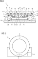
- An X-ray detector 2 described below is designed as a directly converting X-ray detector 2 and is shown in FIG FIG 1 shown schematically in a first embodiment.
- the X-ray detector 2 is part of an X-ray device 4, which is designed as a computer tomograph and is shown in FIG FIG 2 is sketched.
- the x-ray detector 2 is supplemented by an x-ray source 6.
- the x-ray device 4 has a control unit 8.
- the X-ray detector 2 is designed as a directly converting X-ray detector 2 and has a converter layer or sensor layer 10, a first amplifier stage 12, an interposer 14 and an ASIC readout chip 16 as essential components.
- the x-ray detector 2 has a multiplicity of pixels 18 or forms a multiplicity of pixels 18, a volume element 20 of the sensor layer 10 and a signal processing unit 22 belonging to each pixel 18
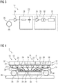
- FIG 3 such a pixel 18 is shown as an example in the form of a simplified block diagram.
- Each signal processing unit 22 in turn is formed in the exemplary embodiment by a first amplifier circuit 24, which is part of the first amplifier stage 12, and a readout circuit 26, which is part of the ASIC readout chip 16, the first amplifier circuit 24 via an interposer connection 28 , which is part of the interposer 14, is connected to the readout circuit 26.
- Pixel 18 has a volume element 20 and a signal processing unit 22 with a first amplifier circuit 24, with an interposer connection 28 and with a readout circuit 26.
- Such an interposer connection 28 typically has a characteristic parasitic capacitance and a characteristic parasitic resistance.
- a sensor signal generated in a volume element 20 of a pixel 18 is first amplified in the first amplifier circuit 24 of the corresponding pixel 18, which is connected to the volume element 20.
- the amplified sensor signal is then forwarded via the interposer connection 28 of this pixel 18 to the ASIC readout chip 16 and processed there in the readout circuit 26 of the pixel 18.
- the signal processing units 22 of the pixels 18 work independently of one another and the X-ray quanta impinging on each pixel 18 are counted, the readout circuit 26 in the ASIC readout chip 16 typically having a comparator 30 and a counting unit 32 for this purpose.
- each readout circuit 26 has a second amplifier circuit 34, and all second amplifier circuits 34 of the ASIC readout chip 16 together form a second amplifier stage.
- FIG 1 a first variant embodiment of the X-ray detector 2 is now shown schematically in a partial sectional view. It can be seen from the illustration that the interposer 14 is interposed between the sensor layer 10 and the ASIC readout chip 16 and that the ASIC readout chip 16 is finally connected in an electrically conductive manner to a circuit board 36 or is connected to the circuit board 36.
- first amplifier stage 12 is interposed between the sensor layer 10 and the interposer 14, with between the sensor layer 10 and the first amplifier stage 12 in the exemplary embodiment simple soldered connections 38 are formed.
- a volume element 20 is connected in an electrically conductive manner to a first amplifier circuit 24 of the first amplifier stage 12 via such a soldered connection 38.
- the first amplifier stage 12 is implemented, for example, on a film that is not explicitly shown, that is, for example, printed on a film, and the film is then laminated, for example, onto the sensor layer 10 or the interposer 14.
- the first amplifier stage 12 is manufactured using a method based on TFT technology and implemented on the interposer 14, which is then preferably designed as a glass interposer.
- FIG. 4 A second variant embodiment of the X-ray detector 2 is shown in FIG FIG 4 shown, at least in a simplified form.
- the first amplifier stage 12 is formed directly on the sensor layer 10, for this purpose a silicon layer or silicon layer is applied to the sensor layer 10 by epitaxy for this purpose and the semiconductor circuits (not shown) that form the first amplifier stage 12 are integrated into this silicon layer or in the silicon layer are realized.
- Silicon is only a suitable example of material.
- gallium arsenide is used as the sensor material of the sensor layer 10
- FIG. 5 Another variant of the X-ray detector 2 is shown in FIG FIG 5 indicated.
- several layers 40, 41, 42 namely a first layer 40, an intermediate layer 41 and a redistribution layer 42, are attached to the sensor layer 10, the first amplifier stage 12 being implemented in the intermediate layer 41. Since the contacting in the embodiment according to FIG 5 ultimately takes place across all three layers 40, 41, 42 shown, in principle all three layers 40, 41, 42 in this exemplary embodiment form the interposer 14, the first amplifier stage 12 being formed in the intermediate layer 41 of this interposer 14.
- FIG 5 It is shown in FIG 5 a basic structure in the area of a pixel 18.
- the volume element 20 of the pixel is initially followed by a metal contact 44. That metal contact 44 is embedded in the first layer 40 made of silicon.
- This first layer 40 is followed by two further layers of silicon, circuit structures 46 which form the first amplifier circuit 24 of this pixel 18 being formed in the intermediate layer 41 by doping.
- the third layer 42 which serves as a redistribution layer 42, has conductor tracks 48 made of copper 48, through which an output 50 of the interposer, which is led to the outside, is positioned such that it is directly connected to an input on the ASIC readout chip 16 via a soldered connection 38 Can be connected in an electrically conductive manner and is also connected in the X-ray detector 2.
- the third embodiment of the X-ray detector 2 according to FIG FIG 5 is furthermore adapted in some cases to the effect that the intermediate layer 41 is replaced by several comparable intermediate layers / intermediate layers.
- the reason for this is then typically that additional wiring, for example for power supply and / or for distributing the signals, is also implemented for the first amplifier circuit 24. Such wiring is then often implemented in several layers.
- FIG. 6 A fourth exemplary embodiment of the X-ray detector 2 is shown in FIG FIG 6 shown schematically.
- the ASIC readout chip 16 is connected to the first amplifier stage 12 via a partly flexible partly rigid circuit board 52, this circuit board 52 functioning as a type of interposer 14.
- the first amplifier stage 12 itself is not more detailed vias shown and soldered connections 38 are electrically conductively connected to the sensor layer 10.
- the first amplifier stage 12 is implemented on a thin, rigid first part 54 of the circuit board 52. It is manufactured in a simple and inexpensive circuit process. That first part 54 of the circuit board 52 is connected via a flexible, second part 56 to another rigid third part 58 to which the ASIC readout chip 16 is connected.
- the ASIC readout chip 16 is manufactured in a more complex and expensive process and implemented on a significantly smaller area.
Landscapes
- Health & Medical Sciences (AREA)
- Life Sciences & Earth Sciences (AREA)
- Physics & Mathematics (AREA)
- High Energy & Nuclear Physics (AREA)
- Molecular Biology (AREA)
- General Physics & Mathematics (AREA)
- Spectroscopy & Molecular Physics (AREA)
- Engineering & Computer Science (AREA)
- Multimedia (AREA)
- Signal Processing (AREA)
- Medical Informatics (AREA)
- Nuclear Medicine, Radiotherapy & Molecular Imaging (AREA)
- Surgery (AREA)
- Optics & Photonics (AREA)
- Pathology (AREA)
- Radiology & Medical Imaging (AREA)
- Biomedical Technology (AREA)
- Heart & Thoracic Surgery (AREA)
- Biophysics (AREA)
- Animal Behavior & Ethology (AREA)
- General Health & Medical Sciences (AREA)
- Public Health (AREA)
- Veterinary Medicine (AREA)
- Measurement Of Radiation (AREA)
- Solid State Image Pick-Up Elements (AREA)
- Apparatus For Radiation Diagnosis (AREA)
Priority Applications (3)
| Application Number | Priority Date | Filing Date | Title |
|---|---|---|---|
| EP19184975.1A EP3764127B1 (fr) | 2019-07-08 | 2019-07-08 | Détecteur de rayons x et appareil à rayons x pourvu de détecteur de rayons x |
| US16/916,686 US11226422B2 (en) | 2019-07-08 | 2020-06-30 | X-ray detector and x-ray device with x-ray detector |
| CN202010644545.1A CN112198543A (zh) | 2019-07-08 | 2020-07-07 | X射线探测器和具有x射线探测器的x射线设备 |
Applications Claiming Priority (1)
| Application Number | Priority Date | Filing Date | Title |
|---|---|---|---|
| EP19184975.1A EP3764127B1 (fr) | 2019-07-08 | 2019-07-08 | Détecteur de rayons x et appareil à rayons x pourvu de détecteur de rayons x |
Publications (3)
| Publication Number | Publication Date |
|---|---|
| EP3764127A1 true EP3764127A1 (fr) | 2021-01-13 |
| EP3764127C0 EP3764127C0 (fr) | 2024-08-28 |
| EP3764127B1 EP3764127B1 (fr) | 2024-08-28 |
Family
ID=67211609
Family Applications (1)
| Application Number | Title | Priority Date | Filing Date |
|---|---|---|---|
| EP19184975.1A Active EP3764127B1 (fr) | 2019-07-08 | 2019-07-08 | Détecteur de rayons x et appareil à rayons x pourvu de détecteur de rayons x |
Country Status (3)
| Country | Link |
|---|---|
| US (1) | US11226422B2 (fr) |
| EP (1) | EP3764127B1 (fr) |
| CN (1) | CN112198543A (fr) |
Families Citing this family (2)
| Publication number | Priority date | Publication date | Assignee | Title |
|---|---|---|---|---|
| DE102022208591B3 (de) | 2022-08-18 | 2023-09-21 | Siemens Healthcare Gmbh | Positionierung von Sensoreinheiten mittels eines Positioniersubstrats und Detektormodul |
| CN118136725A (zh) * | 2023-12-04 | 2024-06-04 | 天芯互联科技有限公司 | 一种光子探测器及其制备方法 |
Citations (4)
| Publication number | Priority date | Publication date | Assignee | Title |
|---|---|---|---|---|
| DE102004057533A1 (de) * | 2004-11-29 | 2006-06-01 | Siemens Ag | Detektorriegel bzw. Detektor, welcher aus mehreren Detektorriegeln gebildet ist und Computertomographiegerät mit einem solchen Detektor |
| JP2009018109A (ja) * | 2007-07-13 | 2009-01-29 | Shimadzu Corp | X線診断装置 |
| DE102012202200B3 (de) | 2012-02-14 | 2013-04-11 | Siemens Aktiengesellschaft | Röntgenstrahlungsdetektor und Verfahren zum Messen von Röntgenstrahlung |
| DE102014204042A1 (de) * | 2014-03-05 | 2015-09-10 | Siemens Aktiengesellschaft | Verfahren zur Ansteuerung eines Röntgendetektors und zugehörige Steuereinheit |
Family Cites Families (19)
| Publication number | Priority date | Publication date | Assignee | Title |
|---|---|---|---|---|
| DE4314336A1 (de) * | 1993-04-30 | 1994-11-03 | Siemens Ag | Flachbildverstärker |
| DE4433036A1 (de) * | 1994-09-16 | 1996-03-21 | Philips Patentverwaltung | Röntgenuntersuchungsgerät |
| JP2004023654A (ja) * | 2002-06-19 | 2004-01-22 | Canon Inc | 放射線撮像装置及び放射線撮像方法 |
| DE10354899B4 (de) * | 2003-11-24 | 2007-07-12 | Siemens Ag | Röntgenvorrichtung und Verfahren zum Herstellen eines Röntgenbilddatensatzes |
| JP2007527999A (ja) * | 2004-03-08 | 2007-10-04 | オー・ツェー・エリコン・バルザース・アクチェンゲゼルシャフト | 増幅層を備えたエリプソメトリックバイオセンサ |
| DE102005047539A1 (de) * | 2005-09-30 | 2007-04-05 | Siemens Ag | Bildverarbeitungsverfahren zur Fensterung und/oder Dosisregelung für medizinische Diagnostikeinrichtungen |
| JP5481260B2 (ja) * | 2009-04-09 | 2014-04-23 | 株式会社東芝 | X線ct装置 |
| PT105039A (pt) * | 2010-04-06 | 2011-10-06 | Univ Nova De Lisboa | Ligas de óxidos tipo p baseados em óxidos de cobre, óxidos estanho, óxidos de ligas de estanho-cobre e respectiva liga metálica, e óxido de níquel, com os respectivos metais embebidos, respectivo processo de fabrico e utilização |
| JP5602598B2 (ja) * | 2010-11-29 | 2014-10-08 | 富士フイルム株式会社 | 放射線検出器及び放射線検出器の製造方法 |
| US9103924B2 (en) * | 2013-10-14 | 2015-08-11 | Nygon As | High throughput detector array |
| JP2015170750A (ja) * | 2014-03-07 | 2015-09-28 | 住友電気工業株式会社 | 光半導体素子及び光半導体素子の製造方法 |
| US9794499B2 (en) * | 2014-04-29 | 2017-10-17 | Fermi Research Alliance, Llc | Wafer-scale pixelated detector system |
| DE102015215085B4 (de) * | 2015-08-07 | 2018-03-01 | Siemens Healthcare Gmbh | Röntgendetektor mit einem einstufigen Vorverstärker mit intrinsischer Pulsformung |
| DE102015218581B4 (de) * | 2015-09-28 | 2019-11-14 | Siemens Healthcare Gmbh | Digital-Analog-Wandler für Mehrschwellenzähler mit Partitionierung der Bits zwischen R-Leiter und Komparator |
| DE102016210935B4 (de) * | 2016-06-20 | 2020-07-09 | Siemens Healthcare Gmbh | Röntgendetektor mit intransparenter Zwischenschicht |
| DE102016221481B4 (de) * | 2016-11-02 | 2021-09-16 | Siemens Healthcare Gmbh | Strahlungsdetektor mit einer Zwischenschicht |
| EP3428692B1 (fr) | 2017-07-10 | 2021-03-10 | Siemens Healthcare GmbH | Détecteur de rayons x comprenant une unité intermédiaire et niveau d'évaluation |
| US10629305B2 (en) * | 2017-11-09 | 2020-04-21 | General Electric Company | Methods and apparatus for self-learning clinical decision support |
| US20190154852A1 (en) * | 2017-11-16 | 2019-05-23 | NueVue Solutions, Inc. | Analog Direct Digital X-Ray Photon Counting Detector For Resolving Photon Energy In Spectral X-Ray CT |
-
2019
- 2019-07-08 EP EP19184975.1A patent/EP3764127B1/fr active Active
-
2020
- 2020-06-30 US US16/916,686 patent/US11226422B2/en active Active
- 2020-07-07 CN CN202010644545.1A patent/CN112198543A/zh active Pending
Patent Citations (4)
| Publication number | Priority date | Publication date | Assignee | Title |
|---|---|---|---|---|
| DE102004057533A1 (de) * | 2004-11-29 | 2006-06-01 | Siemens Ag | Detektorriegel bzw. Detektor, welcher aus mehreren Detektorriegeln gebildet ist und Computertomographiegerät mit einem solchen Detektor |
| JP2009018109A (ja) * | 2007-07-13 | 2009-01-29 | Shimadzu Corp | X線診断装置 |
| DE102012202200B3 (de) | 2012-02-14 | 2013-04-11 | Siemens Aktiengesellschaft | Röntgenstrahlungsdetektor und Verfahren zum Messen von Röntgenstrahlung |
| DE102014204042A1 (de) * | 2014-03-05 | 2015-09-10 | Siemens Aktiengesellschaft | Verfahren zur Ansteuerung eines Röntgendetektors und zugehörige Steuereinheit |
Also Published As
| Publication number | Publication date |
|---|---|
| US11226422B2 (en) | 2022-01-18 |
| EP3764127C0 (fr) | 2024-08-28 |
| CN112198543A (zh) | 2021-01-08 |
| EP3764127B1 (fr) | 2024-08-28 |
| US20210011181A1 (en) | 2021-01-14 |
Similar Documents
| Publication | Publication Date | Title |
|---|---|---|
| DE10307752B4 (de) | Röntgendetektor | |
| DE2609731A1 (de) | Festkoerper-bilderfassungsvorrichtung | |
| EP2207344B1 (fr) | Capteur d'images | |
| DE10142531A1 (de) | Sensoranordnung aus licht- und/oder röntgenstrahlungsempfindlichen Sensoren | |
| DE102016221481A1 (de) | Strahlungsdetektor mit einer Zwischenschicht | |
| EP2057482A1 (fr) | Système et procédé pour intégration de charge | |
| DE102015218581A1 (de) | Digital-Analog-Wandler für Mehrschwellenzähler mit Partitionierung der Bits zwischen R-Leiter und Komparator | |
| EP3764127B1 (fr) | Détecteur de rayons x et appareil à rayons x pourvu de détecteur de rayons x | |
| DE68925946T2 (de) | Festkörperbildmatrix, Vorrichtung und Bildherstellungsverfahren | |
| DE112017005215T5 (de) | Bildaufnahmevorrichtung und elektronische Vorrichtung | |
| DE10359430A1 (de) | Verfahren und Vorrichtung für Röntgenbilddetektoranordnungen | |
| EP3663806B1 (fr) | Détecteur de photons, procédé de fabrication d'un détecteur de photons et appareil à rayons x | |
| DE102004052452B4 (de) | Strahlungsdetektor zur Erfassung von Strahlung | |
| DE102012213092B3 (de) | Übertragungsvorrichtung und Sensor-System | |
| DE112019000268T5 (de) | Integrierte Halbleiterschaltungsvorrichtung, Stromsteuervorrichtung, die die integrierte Halbleiterschaltungsvorrichtung verwendet, und Automatikgetriebesteuervorrichtung, die die Stromsteuervorrichtung verwendet | |
| DE3135740A1 (de) | Photoelektrische umsetzeinrichtung | |
| DE102015215085A1 (de) | Einstufiger Vorverstärker mit intrinsischer Pulsformung | |
| EP1237198A1 (fr) | Capteur de rayonnement et détecteur de rayonnement pour un tomographe assisté par ordinateur | |
| DE102004009627A1 (de) | Schaltung für einen aktiven Pixelsensor | |
| EP1860447B1 (fr) | Dispositif d'essais d'un circuit et procédé d'essais destinés à vérifier un chemin dans un circuit | |
| DE102013206404B3 (de) | Sensorchip, computertomographischer Detektor diesen aufweisend, sowie ein Herstellungsverfahren und ein Betriebsverfahren dafür | |
| DE102009037463B4 (de) | Röntgendetektormodul und Verfahren zu seiner Herstellung | |
| DE102007015643B4 (de) | Verfahren und Vorrichtung zum Übertragen von ausgehenden Nutzsignalen und eines ausgehenden Taktsignals | |
| DE69009882T2 (de) | Festkörperbildsensor. | |
| DE102021114313B4 (de) | Zählen von Pulsen eines elektrischen Signals |
Legal Events
| Date | Code | Title | Description |
|---|---|---|---|
| PUAI | Public reference made under article 153(3) epc to a published international application that has entered the european phase |
Free format text: ORIGINAL CODE: 0009012 |
|
| STAA | Information on the status of an ep patent application or granted ep patent |
Free format text: STATUS: THE APPLICATION HAS BEEN PUBLISHED |
|
| AK | Designated contracting states |
Kind code of ref document: A1 Designated state(s): AL AT BE BG CH CY CZ DE DK EE ES FI FR GB GR HR HU IE IS IT LI LT LU LV MC MK MT NL NO PL PT RO RS SE SI SK SM TR |
|
| AX | Request for extension of the european patent |
Extension state: BA ME |
|
| STAA | Information on the status of an ep patent application or granted ep patent |
Free format text: STATUS: REQUEST FOR EXAMINATION WAS MADE |
|
| 17P | Request for examination filed |
Effective date: 20210713 |
|
| RBV | Designated contracting states (corrected) |
Designated state(s): AL AT BE BG CH CY CZ DE DK EE ES FI FR GB GR HR HU IE IS IT LI LT LU LV MC MK MT NL NO PL PT RO RS SE SI SK SM TR |
|
| STAA | Information on the status of an ep patent application or granted ep patent |
Free format text: STATUS: EXAMINATION IS IN PROGRESS |
|
| 17Q | First examination report despatched |
Effective date: 20220720 |
|
| RAP1 | Party data changed (applicant data changed or rights of an application transferred) |
Owner name: SIEMENS HEALTHINEERS AG |
|
| GRAP | Despatch of communication of intention to grant a patent |
Free format text: ORIGINAL CODE: EPIDOSNIGR1 |
|
| STAA | Information on the status of an ep patent application or granted ep patent |
Free format text: STATUS: GRANT OF PATENT IS INTENDED |
|
| INTG | Intention to grant announced |
Effective date: 20240228 |
|
| GRAS | Grant fee paid |
Free format text: ORIGINAL CODE: EPIDOSNIGR3 |
|
| GRAA | (expected) grant |
Free format text: ORIGINAL CODE: 0009210 |
|
| STAA | Information on the status of an ep patent application or granted ep patent |
Free format text: STATUS: THE PATENT HAS BEEN GRANTED |
|
| AK | Designated contracting states |
Kind code of ref document: B1 Designated state(s): AL AT BE BG CH CY CZ DE DK EE ES FI FR GB GR HR HU IE IS IT LI LT LU LV MC MK MT NL NO PL PT RO RS SE SI SK SM TR |
|
| REG | Reference to a national code |
Ref country code: GB Ref legal event code: FG4D Free format text: NOT ENGLISH |
|
| REG | Reference to a national code |
Ref country code: CH Ref legal event code: EP |
|
| REG | Reference to a national code |
Ref country code: DE Ref legal event code: R096 Ref document number: 502019011971 Country of ref document: DE |
|
| REG | Reference to a national code |
Ref country code: IE Ref legal event code: FG4D Free format text: LANGUAGE OF EP DOCUMENT: GERMAN |
|
| U01 | Request for unitary effect filed |
Effective date: 20240828 |
|
| U07 | Unitary effect registered |
Designated state(s): AT BE BG DE DK EE FI FR IT LT LU LV MT NL PT RO SE SI Effective date: 20240909 |
|
| PG25 | Lapsed in a contracting state [announced via postgrant information from national office to epo] |
Ref country code: NO Free format text: LAPSE BECAUSE OF FAILURE TO SUBMIT A TRANSLATION OF THE DESCRIPTION OR TO PAY THE FEE WITHIN THE PRESCRIBED TIME-LIMIT Effective date: 20241128 |
|
| PG25 | Lapsed in a contracting state [announced via postgrant information from national office to epo] |
Ref country code: PL Free format text: LAPSE BECAUSE OF FAILURE TO SUBMIT A TRANSLATION OF THE DESCRIPTION OR TO PAY THE FEE WITHIN THE PRESCRIBED TIME-LIMIT Effective date: 20240828 Ref country code: GR Free format text: LAPSE BECAUSE OF FAILURE TO SUBMIT A TRANSLATION OF THE DESCRIPTION OR TO PAY THE FEE WITHIN THE PRESCRIBED TIME-LIMIT Effective date: 20241129 |
|
| PG25 | Lapsed in a contracting state [announced via postgrant information from national office to epo] |
Ref country code: IS Free format text: LAPSE BECAUSE OF FAILURE TO SUBMIT A TRANSLATION OF THE DESCRIPTION OR TO PAY THE FEE WITHIN THE PRESCRIBED TIME-LIMIT Effective date: 20241228 |
|
| PG25 | Lapsed in a contracting state [announced via postgrant information from national office to epo] |
Ref country code: HR Free format text: LAPSE BECAUSE OF FAILURE TO SUBMIT A TRANSLATION OF THE DESCRIPTION OR TO PAY THE FEE WITHIN THE PRESCRIBED TIME-LIMIT Effective date: 20240828 |
|
| PG25 | Lapsed in a contracting state [announced via postgrant information from national office to epo] |
Ref country code: ES Free format text: LAPSE BECAUSE OF FAILURE TO SUBMIT A TRANSLATION OF THE DESCRIPTION OR TO PAY THE FEE WITHIN THE PRESCRIBED TIME-LIMIT Effective date: 20240828 Ref country code: RS Free format text: LAPSE BECAUSE OF FAILURE TO SUBMIT A TRANSLATION OF THE DESCRIPTION OR TO PAY THE FEE WITHIN THE PRESCRIBED TIME-LIMIT Effective date: 20241128 |
|
| PG25 | Lapsed in a contracting state [announced via postgrant information from national office to epo] |
Ref country code: RS Free format text: LAPSE BECAUSE OF FAILURE TO SUBMIT A TRANSLATION OF THE DESCRIPTION OR TO PAY THE FEE WITHIN THE PRESCRIBED TIME-LIMIT Effective date: 20241128 Ref country code: PL Free format text: LAPSE BECAUSE OF FAILURE TO SUBMIT A TRANSLATION OF THE DESCRIPTION OR TO PAY THE FEE WITHIN THE PRESCRIBED TIME-LIMIT Effective date: 20240828 Ref country code: NO Free format text: LAPSE BECAUSE OF FAILURE TO SUBMIT A TRANSLATION OF THE DESCRIPTION OR TO PAY THE FEE WITHIN THE PRESCRIBED TIME-LIMIT Effective date: 20241128 Ref country code: IS Free format text: LAPSE BECAUSE OF FAILURE TO SUBMIT A TRANSLATION OF THE DESCRIPTION OR TO PAY THE FEE WITHIN THE PRESCRIBED TIME-LIMIT Effective date: 20241228 Ref country code: HR Free format text: LAPSE BECAUSE OF FAILURE TO SUBMIT A TRANSLATION OF THE DESCRIPTION OR TO PAY THE FEE WITHIN THE PRESCRIBED TIME-LIMIT Effective date: 20240828 Ref country code: GR Free format text: LAPSE BECAUSE OF FAILURE TO SUBMIT A TRANSLATION OF THE DESCRIPTION OR TO PAY THE FEE WITHIN THE PRESCRIBED TIME-LIMIT Effective date: 20241129 Ref country code: ES Free format text: LAPSE BECAUSE OF FAILURE TO SUBMIT A TRANSLATION OF THE DESCRIPTION OR TO PAY THE FEE WITHIN THE PRESCRIBED TIME-LIMIT Effective date: 20240828 |
|
| PG25 | Lapsed in a contracting state [announced via postgrant information from national office to epo] |
Ref country code: SM Free format text: LAPSE BECAUSE OF FAILURE TO SUBMIT A TRANSLATION OF THE DESCRIPTION OR TO PAY THE FEE WITHIN THE PRESCRIBED TIME-LIMIT Effective date: 20240828 |
|
| PG25 | Lapsed in a contracting state [announced via postgrant information from national office to epo] |
Ref country code: CZ Free format text: LAPSE BECAUSE OF FAILURE TO SUBMIT A TRANSLATION OF THE DESCRIPTION OR TO PAY THE FEE WITHIN THE PRESCRIBED TIME-LIMIT Effective date: 20240828 |
|
| PG25 | Lapsed in a contracting state [announced via postgrant information from national office to epo] |
Ref country code: SK Free format text: LAPSE BECAUSE OF FAILURE TO SUBMIT A TRANSLATION OF THE DESCRIPTION OR TO PAY THE FEE WITHIN THE PRESCRIBED TIME-LIMIT Effective date: 20240828 |
|
| PLBE | No opposition filed within time limit |
Free format text: ORIGINAL CODE: 0009261 |
|
| STAA | Information on the status of an ep patent application or granted ep patent |
Free format text: STATUS: NO OPPOSITION FILED WITHIN TIME LIMIT |
|
| 26N | No opposition filed |
Effective date: 20250530 |
|
| U20 | Renewal fee for the european patent with unitary effect paid |
Year of fee payment: 7 Effective date: 20250718 |
|
| REG | Reference to a national code |
Ref country code: CH Ref legal event code: H13 Free format text: ST27 STATUS EVENT CODE: U-0-0-H10-H13 (AS PROVIDED BY THE NATIONAL OFFICE) Effective date: 20260224 |
|
| GBPC | Gb: european patent ceased through non-payment of renewal fee |
Effective date: 20250708 |
|
| PG25 | Lapsed in a contracting state [announced via postgrant information from national office to epo] |
Ref country code: GB Free format text: LAPSE BECAUSE OF NON-PAYMENT OF DUE FEES Effective date: 20250708 |
|
| PG25 | Lapsed in a contracting state [announced via postgrant information from national office to epo] |
Ref country code: CH Free format text: LAPSE BECAUSE OF NON-PAYMENT OF DUE FEES Effective date: 20250731 |