EP3778985A1 - Wolframsilicid-zielelement und verfahren zu seiner herstellung sowie verfahren zur herstellung einer wolframsilicidschicht - Google Patents
Wolframsilicid-zielelement und verfahren zu seiner herstellung sowie verfahren zur herstellung einer wolframsilicidschicht Download PDFInfo
- Publication number
- EP3778985A1 EP3778985A1 EP18912672.5A EP18912672A EP3778985A1 EP 3778985 A1 EP3778985 A1 EP 3778985A1 EP 18912672 A EP18912672 A EP 18912672A EP 3778985 A1 EP3778985 A1 EP 3778985A1
- Authority
- EP
- European Patent Office
- Prior art keywords
- tungsten silicide
- wsi
- silicide target
- grains
- powder
- Prior art date
- Legal status (The legal status is an assumption and is not a legal conclusion. Google has not performed a legal analysis and makes no representation as to the accuracy of the status listed.)
- Pending
Links
Images




Classifications
-
- C—CHEMISTRY; METALLURGY
- C23—COATING METALLIC MATERIAL; COATING MATERIAL WITH METALLIC MATERIAL; CHEMICAL SURFACE TREATMENT; DIFFUSION TREATMENT OF METALLIC MATERIAL; COATING BY VACUUM EVAPORATION, BY SPUTTERING, BY ION IMPLANTATION OR BY CHEMICAL VAPOUR DEPOSITION, IN GENERAL; INHIBITING CORROSION OF METALLIC MATERIAL OR INCRUSTATION IN GENERAL
- C23C—COATING METALLIC MATERIAL; COATING MATERIAL WITH METALLIC MATERIAL; SURFACE TREATMENT OF METALLIC MATERIAL BY DIFFUSION INTO THE SURFACE, BY CHEMICAL CONVERSION OR SUBSTITUTION; COATING BY VACUUM EVAPORATION, BY SPUTTERING, BY ION IMPLANTATION OR BY CHEMICAL VAPOUR DEPOSITION, IN GENERAL
- C23C14/00—Coating by vacuum evaporation, by sputtering or by ion implantation of the coating forming material
- C23C14/22—Coating by vacuum evaporation, by sputtering or by ion implantation of the coating forming material characterised by the process of coating
- C23C14/34—Sputtering
- C23C14/3407—Cathode assembly for sputtering apparatus, e.g. Target
- C23C14/3414—Metallurgical or chemical aspects of target preparation, e.g. casting, powder metallurgy
-
- B—PERFORMING OPERATIONS; TRANSPORTING
- B22—CASTING; POWDER METALLURGY
- B22F—WORKING METALLIC POWDER; MANUFACTURE OF ARTICLES FROM METALLIC POWDER; MAKING METALLIC POWDER; APPARATUS OR DEVICES SPECIALLY ADAPTED FOR METALLIC POWDER
- B22F1/00—Metallic powder; Treatment of metallic powder, e.g. to facilitate working or to improve properties
- B22F1/05—Metallic powder characterised by the size or surface area of the particles
-
- B—PERFORMING OPERATIONS; TRANSPORTING
- B22—CASTING; POWDER METALLURGY
- B22F—WORKING METALLIC POWDER; MANUFACTURE OF ARTICLES FROM METALLIC POWDER; MAKING METALLIC POWDER; APPARATUS OR DEVICES SPECIALLY ADAPTED FOR METALLIC POWDER
- B22F3/00—Manufacture of workpieces or articles from metallic powder characterised by the manner of compacting or sintering; Apparatus specially adapted therefor ; Presses and furnaces
- B22F3/12—Both compacting and sintering
- B22F3/14—Both compacting and sintering simultaneously
- B22F3/15—Hot isostatic pressing
-
- C—CHEMISTRY; METALLURGY
- C01—INORGANIC CHEMISTRY
- C01B—NON-METALLIC ELEMENTS; COMPOUNDS THEREOF; METALLOIDS OR COMPOUNDS THEREOF NOT COVERED BY SUBCLASS C01C
- C01B33/00—Silicon; Compounds thereof
- C01B33/06—Metal silicides
-
- C—CHEMISTRY; METALLURGY
- C22—METALLURGY; FERROUS OR NON-FERROUS ALLOYS; TREATMENT OF ALLOYS OR NON-FERROUS METALS
- C22C—ALLOYS
- C22C1/00—Making non-ferrous alloys
- C22C1/04—Making non-ferrous alloys by powder metallurgy
- C22C1/05—Mixtures of metal powder with non-metallic powder
-
- C—CHEMISTRY; METALLURGY
- C22—METALLURGY; FERROUS OR NON-FERROUS ALLOYS; TREATMENT OF ALLOYS OR NON-FERROUS METALS
- C22C—ALLOYS
- C22C27/00—Alloys based on rhenium or a refractory metal not mentioned in groups C22C14/00 or C22C16/00
- C22C27/04—Alloys based on tungsten or molybdenum
-
- C—CHEMISTRY; METALLURGY
- C22—METALLURGY; FERROUS OR NON-FERROUS ALLOYS; TREATMENT OF ALLOYS OR NON-FERROUS METALS
- C22C—ALLOYS
- C22C32/00—Non-ferrous alloys containing at least 5% by weight but less than 50% by weight of oxides, carbides, borides, nitrides, silicides or other metal compounds, e.g. oxynitrides, sulfides, whether added as such or formed in situ
- C22C32/0047—Non-ferrous alloys containing at least 5% by weight but less than 50% by weight of oxides, carbides, borides, nitrides, silicides or other metal compounds, e.g. oxynitrides, sulfides, whether added as such or formed in situ with carbides, nitrides, borides or silicides as the main non-metallic constituents
- C22C32/0078—Non-ferrous alloys containing at least 5% by weight but less than 50% by weight of oxides, carbides, borides, nitrides, silicides or other metal compounds, e.g. oxynitrides, sulfides, whether added as such or formed in situ with carbides, nitrides, borides or silicides as the main non-metallic constituents only silicides
-
- C—CHEMISTRY; METALLURGY
- C23—COATING METALLIC MATERIAL; COATING MATERIAL WITH METALLIC MATERIAL; CHEMICAL SURFACE TREATMENT; DIFFUSION TREATMENT OF METALLIC MATERIAL; COATING BY VACUUM EVAPORATION, BY SPUTTERING, BY ION IMPLANTATION OR BY CHEMICAL VAPOUR DEPOSITION, IN GENERAL; INHIBITING CORROSION OF METALLIC MATERIAL OR INCRUSTATION IN GENERAL
- C23C—COATING METALLIC MATERIAL; COATING MATERIAL WITH METALLIC MATERIAL; SURFACE TREATMENT OF METALLIC MATERIAL BY DIFFUSION INTO THE SURFACE, BY CHEMICAL CONVERSION OR SUBSTITUTION; COATING BY VACUUM EVAPORATION, BY SPUTTERING, BY ION IMPLANTATION OR BY CHEMICAL VAPOUR DEPOSITION, IN GENERAL
- C23C14/00—Coating by vacuum evaporation, by sputtering or by ion implantation of the coating forming material
- C23C14/06—Coating by vacuum evaporation, by sputtering or by ion implantation of the coating forming material characterised by the coating material
- C23C14/0682—Silicides
-
- C—CHEMISTRY; METALLURGY
- C23—COATING METALLIC MATERIAL; COATING MATERIAL WITH METALLIC MATERIAL; CHEMICAL SURFACE TREATMENT; DIFFUSION TREATMENT OF METALLIC MATERIAL; COATING BY VACUUM EVAPORATION, BY SPUTTERING, BY ION IMPLANTATION OR BY CHEMICAL VAPOUR DEPOSITION, IN GENERAL; INHIBITING CORROSION OF METALLIC MATERIAL OR INCRUSTATION IN GENERAL
- C23C—COATING METALLIC MATERIAL; COATING MATERIAL WITH METALLIC MATERIAL; SURFACE TREATMENT OF METALLIC MATERIAL BY DIFFUSION INTO THE SURFACE, BY CHEMICAL CONVERSION OR SUBSTITUTION; COATING BY VACUUM EVAPORATION, BY SPUTTERING, BY ION IMPLANTATION OR BY CHEMICAL VAPOUR DEPOSITION, IN GENERAL
- C23C14/00—Coating by vacuum evaporation, by sputtering or by ion implantation of the coating forming material
- C23C14/22—Coating by vacuum evaporation, by sputtering or by ion implantation of the coating forming material characterised by the process of coating
- C23C14/34—Sputtering
- C23C14/35—Sputtering by application of a magnetic field, e.g. magnetron sputtering
-
- C—CHEMISTRY; METALLURGY
- C23—COATING METALLIC MATERIAL; COATING MATERIAL WITH METALLIC MATERIAL; CHEMICAL SURFACE TREATMENT; DIFFUSION TREATMENT OF METALLIC MATERIAL; COATING BY VACUUM EVAPORATION, BY SPUTTERING, BY ION IMPLANTATION OR BY CHEMICAL VAPOUR DEPOSITION, IN GENERAL; INHIBITING CORROSION OF METALLIC MATERIAL OR INCRUSTATION IN GENERAL
- C23C—COATING METALLIC MATERIAL; COATING MATERIAL WITH METALLIC MATERIAL; SURFACE TREATMENT OF METALLIC MATERIAL BY DIFFUSION INTO THE SURFACE, BY CHEMICAL CONVERSION OR SUBSTITUTION; COATING BY VACUUM EVAPORATION, BY SPUTTERING, BY ION IMPLANTATION OR BY CHEMICAL VAPOUR DEPOSITION, IN GENERAL
- C23C16/00—Chemical coating by decomposition of gaseous compounds, without leaving reaction products of surface material in the coating, i.e. chemical vapour deposition [CVD] processes
- C23C16/44—Chemical coating by decomposition of gaseous compounds, without leaving reaction products of surface material in the coating, i.e. chemical vapour deposition [CVD] processes characterised by the method of coating
- C23C16/4417—Methods specially adapted for coating powder
-
- C—CHEMISTRY; METALLURGY
- C23—COATING METALLIC MATERIAL; COATING MATERIAL WITH METALLIC MATERIAL; CHEMICAL SURFACE TREATMENT; DIFFUSION TREATMENT OF METALLIC MATERIAL; COATING BY VACUUM EVAPORATION, BY SPUTTERING, BY ION IMPLANTATION OR BY CHEMICAL VAPOUR DEPOSITION, IN GENERAL; INHIBITING CORROSION OF METALLIC MATERIAL OR INCRUSTATION IN GENERAL
- C23C—COATING METALLIC MATERIAL; COATING MATERIAL WITH METALLIC MATERIAL; SURFACE TREATMENT OF METALLIC MATERIAL BY DIFFUSION INTO THE SURFACE, BY CHEMICAL CONVERSION OR SUBSTITUTION; COATING BY VACUUM EVAPORATION, BY SPUTTERING, BY ION IMPLANTATION OR BY CHEMICAL VAPOUR DEPOSITION, IN GENERAL
- C23C16/00—Chemical coating by decomposition of gaseous compounds, without leaving reaction products of surface material in the coating, i.e. chemical vapour deposition [CVD] processes
- C23C16/44—Chemical coating by decomposition of gaseous compounds, without leaving reaction products of surface material in the coating, i.e. chemical vapour deposition [CVD] processes characterised by the method of coating
- C23C16/442—Chemical coating by decomposition of gaseous compounds, without leaving reaction products of surface material in the coating, i.e. chemical vapour deposition [CVD] processes characterised by the method of coating using fluidised bed process
-
- C—CHEMISTRY; METALLURGY
- C23—COATING METALLIC MATERIAL; COATING MATERIAL WITH METALLIC MATERIAL; CHEMICAL SURFACE TREATMENT; DIFFUSION TREATMENT OF METALLIC MATERIAL; COATING BY VACUUM EVAPORATION, BY SPUTTERING, BY ION IMPLANTATION OR BY CHEMICAL VAPOUR DEPOSITION, IN GENERAL; INHIBITING CORROSION OF METALLIC MATERIAL OR INCRUSTATION IN GENERAL
- C23C—COATING METALLIC MATERIAL; COATING MATERIAL WITH METALLIC MATERIAL; SURFACE TREATMENT OF METALLIC MATERIAL BY DIFFUSION INTO THE SURFACE, BY CHEMICAL CONVERSION OR SUBSTITUTION; COATING BY VACUUM EVAPORATION, BY SPUTTERING, BY ION IMPLANTATION OR BY CHEMICAL VAPOUR DEPOSITION, IN GENERAL
- C23C16/00—Chemical coating by decomposition of gaseous compounds, without leaving reaction products of surface material in the coating, i.e. chemical vapour deposition [CVD] processes
- C23C16/44—Chemical coating by decomposition of gaseous compounds, without leaving reaction products of surface material in the coating, i.e. chemical vapour deposition [CVD] processes characterised by the method of coating
- C23C16/50—Chemical coating by decomposition of gaseous compounds, without leaving reaction products of surface material in the coating, i.e. chemical vapour deposition [CVD] processes characterised by the method of coating using electric discharges
- C23C16/513—Chemical coating by decomposition of gaseous compounds, without leaving reaction products of surface material in the coating, i.e. chemical vapour deposition [CVD] processes characterised by the method of coating using electric discharges using plasma jets
-
- H—ELECTRICITY
- H01—ELECTRIC ELEMENTS
- H01J—ELECTRIC DISCHARGE TUBES OR DISCHARGE LAMPS
- H01J37/00—Discharge tubes with provision for introducing objects or material to be exposed to the discharge, e.g. for the purpose of examination or processing thereof
- H01J37/32—Gas-filled discharge tubes
- H01J37/34—Gas-filled discharge tubes operating with cathodic sputtering
- H01J37/3411—Constructional aspects of the reactor
- H01J37/3414—Targets
- H01J37/3426—Material
-
- H—ELECTRICITY
- H01—ELECTRIC ELEMENTS
- H01J—ELECTRIC DISCHARGE TUBES OR DISCHARGE LAMPS
- H01J37/00—Discharge tubes with provision for introducing objects or material to be exposed to the discharge, e.g. for the purpose of examination or processing thereof
- H01J37/32—Gas-filled discharge tubes
- H01J37/34—Gas-filled discharge tubes operating with cathodic sputtering
- H01J37/3411—Constructional aspects of the reactor
- H01J37/3414—Targets
- H01J37/3426—Material
- H01J37/3429—Plural materials
-
- H—ELECTRICITY
- H01—ELECTRIC ELEMENTS
- H01J—ELECTRIC DISCHARGE TUBES OR DISCHARGE LAMPS
- H01J37/00—Discharge tubes with provision for introducing objects or material to be exposed to the discharge, e.g. for the purpose of examination or processing thereof
- H01J37/32—Gas-filled discharge tubes
- H01J37/34—Gas-filled discharge tubes operating with cathodic sputtering
- H01J37/3488—Constructional details of particle beam apparatus not otherwise provided for, e.g. arrangement, mounting, housing, environment; special provisions for cleaning or maintenance of the apparatus
- H01J37/3491—Manufacturing of targets
-
- H—ELECTRICITY
- H10—SEMICONDUCTOR DEVICES; ELECTRIC SOLID-STATE DEVICES NOT OTHERWISE PROVIDED FOR
- H10P—GENERIC PROCESSES OR APPARATUS FOR THE MANUFACTURE OR TREATMENT OF DEVICES COVERED BY CLASS H10
- H10P14/00—Formation of materials, e.g. in the shape of layers or pillars
- H10P14/40—Formation of materials, e.g. in the shape of layers or pillars of conductive or resistive materials
- H10P14/42—Formation of materials, e.g. in the shape of layers or pillars of conductive or resistive materials using a gas or vapour
-
- B—PERFORMING OPERATIONS; TRANSPORTING
- B22—CASTING; POWDER METALLURGY
- B22F—WORKING METALLIC POWDER; MANUFACTURE OF ARTICLES FROM METALLIC POWDER; MAKING METALLIC POWDER; APPARATUS OR DEVICES SPECIALLY ADAPTED FOR METALLIC POWDER
- B22F2301/00—Metallic composition of the powder or its coating
- B22F2301/20—Refractory metals
-
- B—PERFORMING OPERATIONS; TRANSPORTING
- B22—CASTING; POWDER METALLURGY
- B22F—WORKING METALLIC POWDER; MANUFACTURE OF ARTICLES FROM METALLIC POWDER; MAKING METALLIC POWDER; APPARATUS OR DEVICES SPECIALLY ADAPTED FOR METALLIC POWDER
- B22F2302/00—Metal Compound, non-Metallic compound or non-metal composition of the powder or its coating
- B22F2302/45—Others, including non-metals
-
- B—PERFORMING OPERATIONS; TRANSPORTING
- B22—CASTING; POWDER METALLURGY
- B22F—WORKING METALLIC POWDER; MANUFACTURE OF ARTICLES FROM METALLIC POWDER; MAKING METALLIC POWDER; APPARATUS OR DEVICES SPECIALLY ADAPTED FOR METALLIC POWDER
- B22F2304/00—Physical aspects of the powder
- B22F2304/10—Micron size particles, i.e. above 1 micrometer up to 500 micrometer
-
- B—PERFORMING OPERATIONS; TRANSPORTING
- B22—CASTING; POWDER METALLURGY
- B22F—WORKING METALLIC POWDER; MANUFACTURE OF ARTICLES FROM METALLIC POWDER; MAKING METALLIC POWDER; APPARATUS OR DEVICES SPECIALLY ADAPTED FOR METALLIC POWDER
- B22F2998/00—Supplementary information concerning processes or compositions relating to powder metallurgy
- B22F2998/10—Processes characterised by the sequence of their steps
-
- C—CHEMISTRY; METALLURGY
- C01—INORGANIC CHEMISTRY
- C01P—INDEXING SCHEME RELATING TO STRUCTURAL AND PHYSICAL ASPECTS OF SOLID INORGANIC COMPOUNDS
- C01P2006/00—Physical properties of inorganic compounds
- C01P2006/90—Other properties not specified above
-
- C—CHEMISTRY; METALLURGY
- C23—COATING METALLIC MATERIAL; COATING MATERIAL WITH METALLIC MATERIAL; CHEMICAL SURFACE TREATMENT; DIFFUSION TREATMENT OF METALLIC MATERIAL; COATING BY VACUUM EVAPORATION, BY SPUTTERING, BY ION IMPLANTATION OR BY CHEMICAL VAPOUR DEPOSITION, IN GENERAL; INHIBITING CORROSION OF METALLIC MATERIAL OR INCRUSTATION IN GENERAL
- C23C—COATING METALLIC MATERIAL; COATING MATERIAL WITH METALLIC MATERIAL; SURFACE TREATMENT OF METALLIC MATERIAL BY DIFFUSION INTO THE SURFACE, BY CHEMICAL CONVERSION OR SUBSTITUTION; COATING BY VACUUM EVAPORATION, BY SPUTTERING, BY ION IMPLANTATION OR BY CHEMICAL VAPOUR DEPOSITION, IN GENERAL
- C23C14/00—Coating by vacuum evaporation, by sputtering or by ion implantation of the coating forming material
- C23C14/22—Coating by vacuum evaporation, by sputtering or by ion implantation of the coating forming material characterised by the process of coating
- C23C14/34—Sputtering
Definitions
- the present invention relates to a tungsten silicide target, a method for manufacturing the same, and a method for manufacturing a tungsten silicide film.
- a sputtering method is used in order to form a thin film in a manufacturing step of a semiconductor device.
- the sputtering method provides improved mass productivity and stability of deposition, and forms a thin film by allowing Ar ions to collide with a target to release metals as target materials and allowing the released metals to deposit onto a substrate opposing to the target.
- Patent Literature 1 describes a sputtering target made of tungsten silicide, which has an average surface roughness Ra of a target material of more than 1.0 and 2.0 ⁇ m or less.
- the tungsten silicide target according to the present embodiment is a tungsten silicide target having a two-phase structure of a WSi 2 phase and a Si phase, wherein the tungsten silicide target is represented by a composition formula in an atomic ratio: WSi x with X > 2.0; wherein, when observing a sputtering surface, a ratio of a total area I1 of Si grains having an area per a Si grain of 63.6 ⁇ m 2 or more to a total area S1 of the Si grains forming the Si phase (I1/S1) is 5% or less; and wherein a Weibull modulus of flexural strength is 2.1 or more.
- a ratio of a total area I2 of WSi 2 grains having an area per a WSi 2 grain of 63.6 ⁇ m 2 or more to a total area S2 of the WSi 2 grains forming the WSi 2 phase is 5% or less.
- the ratio of the total area I2 of the WSi 2 grains having the area per a WSi 2 grain of 63.6 ⁇ m 2 or more to the total area S2 of the WSi 2 grains forming the WSi 2 phase (I2/S2) is 0.1% or less.
- an average area per a WSi 2 grain is 6.0 ⁇ m 2 or less.
- the average area per a WSi 2 grain is 3.0 ⁇ m 2 or less.
- an average area per a Si grain is less than 2.5 ⁇ m 2 .
- the average area per a Si grain is 1.2 ⁇ m 2 or more.
- the average flexural strength is 250 MPa or more.
- the tungsten silicide target according to the present embodiment has an oxygen concentration of 700 ppm by mass or more.
- the tungsten silicide target according to the present embodiment has a relative density of 99.9% or more.
- the method for manufacturing the tungsten silicide target according to the present embodiment is a method for manufacturing the above tungsten silicide target, the method comprising: a preparing step comprising mixing W powder with Si powder such that an atomic ratio Si/W is larger than 2.0, and causing a siliciding synthesis to prepare mixed powder in which WSi 2 phases and Si phases are combined to form individual grains; a pulverizing step of pulverizing the mixed powder, ,; and a sintering step of subjecting the pulverized mixed powder to hot-pressing sintering to provide a sintered body.
- the W powder has a BET value of 1.0 m 2 /g or less.
- the Si powder has a BET value of 2.5 m 2 /g or less.
- the pulverizing step comprises pulverizing the mixed powder such that the BET value of the pulverized grains is 1.0 m 2 /g or less.
- a method for manufacturing a tungsten silicide film according to an embodiment of the present invention comprises a deposition step of carrying out sputtering using the above tungsten silicide target.
- the tungsten silicide target of the present embodiment it is possible to provide a tungsten silicide target that efficiently suppresses generation of particles during deposition
- a BET value refers to a value measured by a gas adsorption method (a BET method) according to JIS Z 8830: 2013 (ISO 9277: 2010).
- the BET value is the total surface area per unit weight (1 g) of powder to be measured and is expressed in a unit of square meter, and is also referred to as a specific surface area (m 2 /g). Therefore, finer powder results in a higher surface area, thereby providing a higher BET value.
- the present inventors have found that a decreased proportion of Si grains having an area higher than a predetermined value and a Weibull modulus of flexural strength having an intended value or more lead to a tungsten silicide target that is densified and has uniformly dispersed grains without being coarsened, whereby the tungsten silicide target that can efficiently suppress particles during deposition can be obtained.
- the tungsten silicide target according to this embodiment will be described below.
- the tungsten silicide target of the present embodiment it is possible to efficiently suppress the generation of particles during deposition.
- the tungsten silicide target according to the embodiment has a two-phase structure of a WSi 2 phase and a Si phase, and has a composition formula in atomic ratio represented by WSi x with X > 2.0.
- the tungsten silicide target according to an embodiment of the present invention contains WSi 2 grains forming the WSi 2 phases and Si grains forming the Si phases. For a decrease in the particles, areas of the Si grains are more related with the generation of the particles than areas of the WSi 2 grains. This will lead to irregularities (in an erosion direction) on a sputtering surface due to preferential sputtering of the Si grains because the Si grains on the sputtering surface are more easily sputtered than the WSi 2 grains. As the irregularities becomes larger, abnormal discharge is easily generated during sputtering, so that the number of particles increases. Therefore, the tungsten silicide target is required to have a smaller Si grain area.
- a ratio of a total area I1 of Si grains having an area per a Si grain of 63.6 ⁇ m 2 or more to a total area S1 of the Si grains forming the Si phase is 5% or less, and preferably 2.5% or less, and more preferably 0.5% or less. This can allow the irregularities on the sputtering surface caused by preferential sputtering of the Si grains to be decreased, so that the generation of the particles during sputtering can be efficiently suppressed.
- a texture image is observed on the sputtering surface of the tungsten silicide target using SEM.
- the areas of the Si grains are calculated by obtaining an SEM image of the sputtering surface of the tungsten silicide target and then analyzing the image with analysis software.
- an average area per a Si grain is less than 5.0 ⁇ m 2 , and preferably less than 3.2 ⁇ m 2 , and even more preferably less than 2.5 ⁇ m 2 , and still more preferably less than 2.0 ⁇ m 2 , in terms of suppressing the generation of the particles during sputtering.
- the average area per a Si grain is preferably 1.2 ⁇ m 2 or more, and more preferably 1.5 ⁇ m 2 or more, and still more preferably 1.8 ⁇ m 2 or more.
- the average area per a Si grain is calculated by obtaining a SEM image of a sputtering surface of the tungsten silicide target and then analyzing the image with analysis software.
- the WSi 2 grains forming the WSi 2 phases have different sputtering rates which are indices for forming a film, depending on crystal orientations. If the WSi 2 grains are larger, erosion progresses only at a specific portion due to a difference of crystal orientations to increase the irregularities (in the erosion direction) on the sputtering surface, so that the particles are generated. For this reason, the areas of WSi 2 grains are required to be decreased, as with the areas of the Si grains.
- a ratio of a total area I2 of WSi 2 grains having an area per a WSi 2 grain of 63.6 ⁇ m 2 or more to a total area S2 of the WSi 2 grains forming the WSi 2 phase is 5% or less, and preferably 2.5% or less, and more preferably 0.5% or less, and still more preferably 0.1% or less.
- a crystal orientation is defined for the sputtering surface of the tungsten silicide target by electron beam backscattering diffraction (EBSD).
- EBSD electron beam backscattering diffraction
- the Kikuchi line is generated.
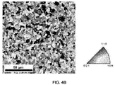
- the area per a WSi 2 grain is calculated by specifying a grain size of the WSi 2 phase by identifying a boundary having a plane orientation difference of 15° or more as a crystal grain boundary utilizing the fact that the WSi 2 grains have random orientations.
- an average equivalent circle diameter in the area of 63.6 ⁇ m 2 per a WSi 2 grain is 9 ⁇ m.
- an average area per a WSi 2 grain when observing the sputtering surface, is preferably 6.0 ⁇ m 2 or less, and more preferably 4.8 ⁇ m 2 or less, and still more preferably 3.7 ⁇ m 2 or less, in terms of suppressing the generation of the particles during sputtering.
- the average area per a WSi 2 grain when observing the sputtered surface, is preferably 3.0 ⁇ m 2 or more, and more preferably 3.2 ⁇ m 2 or more, and even more preferably 3.3 ⁇ m 2 or more.
- the average area per a WSi 2 grain is calculated on the sputtering surface of the tungsten silicide target by EBSD in the same manner as described above.
- an average flexural strength is preferably 250 MPa or more, and more preferably 280 MPa or more, and even more preferably 350 MPa or more, in order to prevent cracking, chipping, or the like during sputtering and to suppress the generation of the particles.
- the average flexural strength is an average value of flexural strengths measured at five or more points on the sputtering target using a tensile compression tester in accordance with "JIS R 1601: 2008 Testing method for flexural strength (modulus of rupture) of fine ceramics at room temperature".
- a Weibull Modulus of the flexural strength is 2.1 or more, and preferably 2.3 or more, and even more preferably 2.7 or more, in terms of increasing the uniformity of the tungsten silicide target and eliminating internal defects.
- the Weibull Modulus indicates an amount of fine pores which do not show as a difference in the relative density and have very slight ratio of a volume to the total volume. The slight pores cause stress concentration points, leading to easy breakage of a material starting from the pores. Therefore, a lower Weibull Modulus means that there are many fine pores, and a higher Weibull Modulus means that there are less fine pores.
- the characteristics of the tungsten silicide target according to the present embodiment are represented by the Weibull Modulus of the flexural strength.
- Weibull Modulus is measured in accordance with "JIS R 1625: 2010 Weibull statistical analysis of strength data for fine ceramics.
- the oxygen concentration in the tungsten silicide target is always 700 ppm by mass or more, which is generally an unavoidable oxygen concentration when finely pulverized by a pulverizing method such as a jet mill to obtain fine raw material powder.
- the oxygen concentration can be utilized as an index indicating that sufficient refinement has been achieved. From this viewpoint, the oxygen concentration is preferably 700 ppm by mass or more, and more preferably 1000 ppm by mass or more, which is considered to be capable of achieving further refinement.
- the oxygen concentration in the tungsten silicide target is preferably 5000 ppm by mass or less, and more preferably 3000 ppm by mass or less, and even more preferably 2500 ppm by mass or less, in terms of preventing excessive generation of an oxide which is originally a cause of micro-arcing and is considered to generate the particles. It is noted that in the present specification, the oxygen concentration in the tungsten silicide target is measured by an inert gas melting-infrared absorption method.
- the semi-sintered low oxygen portion refers to sponge-shaped tungsten silicide that remains after the silicon that has existed inside the sintered region disappears due to volatilization as silicon monoxide with adsorbed oxygen.
- tungsten silicide target according to the present embodiment has substantially no void in the sintered body, and thus preferably has a relative density of 99.9% or more.
- the total concentration of impurities other than oxygen is 0.1% by mass or less, and preferably 0.01% by mass, and more preferably 0.001 % by mass or less, so as not to be incorporated as impurities in the formed tungsten silicide layer.
- Tungsten and silicon having a purity of 5 to 9 N are easily available from the market as raw materials, and the use of such a high-purity raw material can easily achieve the total concentration of impurities other than oxide in the tungsten silicide target produced of 0.001% by mass or less.
- the concentration of impurities other than oxygen is measured by the GDMS method, and the elements to be measured are Fe, Al, Ni, Cu, Cr, Co, K, Na, U, and Th.
- the tungsten silicide target according to the present embodiment can be used by processing it into any shape, including, but not limited to, a disk shape, a rectangular plate shape, a cylindrical shape, and the like.
- the tungsten silicide target according to the present embodiment may be joined to a backing plate.
- the target and the backing plate may be joined by any known method, for example, using a low melting point solder such as indium solder, tin solder, and tin alloy solder.
- a low melting point solder such as indium solder, tin solder, and tin alloy solder.
- Any known material may be used as a material of the backing plate, including, for example, copper (for example, oxygen-free copper), copper alloys, aluminum alloys, titanium, stainless steel, and the like.
- the tungsten silicide target according to this embodiment can be used as, but not limited to, a tungsten silicide target for forming electrodes, wirings, and contact barriers of semiconductor devices such as LSIs.
- a sputtering device that can be used by the tungsten silicide target according to the present embodiment.
- a magnetron sputtering device, an RF application type magnetron DC sputtering device or the like can be used.
- FIG. 1 is a flowchart showing an outline of a method for manufacturing a tungsten silicide target according to an embodiment of the present invention. As shown in FIG. 1
- the method for manufacturing the tungsten silicide target according to the present embodiment includes a step S101 of refining raw material powder (W powder and Si powder) (hereinafter, referred to as a "refining step”); a step S102 of preparing mixed powder of WSi 2 grains and Si grains (hereinafter, referred to as a "preparing step”); a step S103 of pulverizing the mixed powder (hereinafter, referred to as a “pulverizing step”); a step S104 of sintering the pulverized mixed powder (hereinafter, referred to as a “sintering step”); and a step S105 of machining the sintered body (hereinafter, referred to as a "machining step”).
- a step S101 of refining raw material powder W powder and Si powder
- a step S102 of preparing mixed powder of WSi 2 grains and Si grains hereinafter, referred to as a "preparing step”
- both of the W powder and the Si powder which are the raw material powders, are placed in a pulverizing device and pulverized, or the W powder and the Si powder are separately placed in a pulverizing device and pulverized.
- the sizes of the W powder and the Si powder are reflected in the sizes of the WSi 2 grains and the Si grains in the tungsten silicide target, which affects the refinement of the structure. Therefore, when manufacturing the tungsten silicide target, the W powder and the Si powder are previously made finer in order to control the sizes of the WSi 2 powder and the Si powder which can make up the material.
- the W powder and the Si powder are preferably pulverized by a pulverizing device so as to have the following BET value.
- the BET value of the W powder is preferably 1.0 m 2 /g or less, and more preferably 0.9 m 2 /g or less, and even more preferably 0.7 m 2 /g or less, and still more preferably 0.4 m 2 /g or less.
- the BET value of the Si powder is preferably 2.5 m 2 /g or less, and more preferably 2.2 m 2 /g or less, and even more preferably 2.0 m 2 /g or less, and still more preferably 1.9 m 2 /g or less.
- each BET value of the W powder and the Si powder is preferably 0.1 m 2 /g or more.
- the W powder and the Si powder which, for example, have a purity of 99.9% by mass or more, and preferably 99.99% by mass or more, and more preferably 99.999% by mass or more.
- those having the BET value in the suitable range are currently commercially available. Therefore, the commercially available products may be used.
- the pulverizing device is not particularly limited as long as the W powder and the Si powder can be pulverized, examples being a ball mill, a multi-stirring blade rotary type medium stirring mill, a jet mill, and a planetary ball mill.
- the pulverization is preferably carried out in an atmosphere of an inert gas such as nitrogen or argon to suppress unnecessary oxidation.
- an inert gas such as nitrogen or argon to suppress unnecessary oxidation.
- non-standard coarse grains may be removed by sieving them with a sieve having an intended opening or by a gas phase classifier.
- mixed powder in which the WSi 2 phases and the Si phases are combined to form individual grains is prepared, including mixing the W powder with the Si powder such that an atomic ratio of Si/W is, for example, higher than 2.0, and carrying out a silicide synthesis under intended conditions (synthesis temperature, synthesis time, vacuum pressure).
- the synthesis temperature is, for example, preferably from 1200 to 1400°C, and more preferably from 1250 to 1350°C, and still more preferably from 1270 to 1320°C.
- the synthesis time is, for example, from 1 to 6 hours, and preferably from 2 to 5 hours, and more preferably from 3 to 4 hours.
- the vacuum pressure is, for example, preferably 1.0 Pa or less, and more preferably 1.0 x 10 -2 Pa or less, and still more preferably 1.0 x 10 -4 Pa or less.
- a predetermined amount of the refined W powder and Si powder are weighed and mixed in a container, and a silicidation synthesis is then caused in a synthesis furnace.
- the silicidation synthesis provides mixed powder in which the WSi 2 phases and the Si phases are combined to form individual grains.
- the synthesis proceeds until the pure W phases disappear, resulting in the mixed powder in which only the WSi 2 phases and the Si phases remain.
- the mixed powder is pulverized by the pulverizing device to obtain pulverized mixed powder.
- the sizes of grains in the mixed powder is reflected in the sizes of the WSi 2 grains and the Si grains in the target, which affects the refinement of the structure. Therefore, the mixed powder is pulverized such that a BET value of the pulverized grains is preferably 1.0 m 2 /g or less, and more preferably 0.8 m 2 /g or less, and even more preferably 0.6 m 2 /g or less, for example, it can be from 0.1 to 1.0 m 2 /g.
- the pulverizing device is not particularly limited as long as it can pulverize the mixed powder, examples being a ball mill, a multi-stirring blade rotary type medium stirring mill, a jet mill, and a planetary ball mill.
- the pulverization is preferably carried out in an atmosphere of an inert gas such as nitrogen or argon to suppress unnecessary oxidation.
- non-standard coarse grains may be removed by sieving them with a sieve having an intended opening or by a gas phase classifier.
- an oxygen concentration of the pulverized grains is adjusted to 500 ppm by mass to 3000 ppm by mass, and preferably 700 ppm by mass to 2700 ppm by mass, and more preferably 1500 ppm by mass to 2500 ppm by mass, prior to sintering, because it is easy to control the oxygen concentration in the target obtained after the sintering to a target range. Therefore, when the oxygen concentration of the mixed powder before pulverization is too high or the like, the pulverizing step S103 of pulverizing the mixed powder may be carried out after deoxygenation by heating the WSi 2 powder and the Si powder in a separate manner or in a mixed state under vacuum.
- the mixed powder obtained by synthesizing tungsten silicide to form individual grains can be pulverized to obtain the WSi 2 powder, which is then mixed with the Si powder to obtain the pulverized mixed powder of the WSi 2 powder and the Si powder.
- a V-type mixer, a pot mill, a ball mill, a planetary ball mill or the like may be preferably used.
- a method for manufacturing a tungsten silicide film according to an embodiment according to the present invention includes: a deposition step of carrying out sputtering with a sputtering device using the above tungsten silicide target according to the embodiment.
- the tungsten silicide film is used as an LSI electrode and wiring.
- a thickness of the tungsten silicide film may be optionally changed depending on applications to be used.
- the adsorption isotherm was obtained with a specific surface area measuring device (Macsorb® HM model-1201, from Mountech Co., Ltd.), using a He-N 2 gas and liquid nitrogen at -196°C as a refrigerant, under a pretreatment conditions of heating at 200°C for 0.5 hour, and under a measured relative pressure of 0.05 ⁇ P/Po ⁇ 0.3.
- the median diameter D50 is indicated by a grain diameter at the time when the cumulative volume is 50%.
- W powder having a BET value of from 0.75 to 0.85 m 2 /g and a purity of 5N was prepared.
- Si raw material powder having a BET value of from 1.8 to 2.0 m 2 /g was prepared.
- tungsten silicide was subjected to evacuation up to 5 ⁇ 10 -4 Torr, and synthesis was then carried out at 1250 to 1390°C for 1 to 5 hours.
- the interior of the furnace was allowed to cool, and the resulting product was removed from the furnace at the time when the temperature was decreased to 50°C, to obtain mixed powder in which the WSi 2 phases and the Si phases were combined to form individual grains.
- the resulting mixed powder was processed by a jet mill in an inert gas atmosphere, and classified such that the pulverized grains had a median diameter D50 of 4.9 ⁇ m or less. As a result, as shown in Table 1, the characteristics of the pulverized grains were obtained.
- the median diameter D50 of the pulverized grains was calculated by ultrasonic dispersion measurement in ultrapure water using a laser diffraction/scattering particle size distribution analyzer (HORIBA, Partica mini LA-350).
- the retention time refers to a time to maintain the pressing temperature after reaching the predetermined pressing temperature.
- the pressed product was taken out and machined into a disk-shaped tungsten silicide target having a diameter of 164 mm and a thickness of 5 mm.
- An area of the sputtering surface of the target is 211 cm 2 .
- An oxygen concentration of the resulting tungsten silicide target is shown in Table 2.
- an actual density pr of the resulting tungsten silicide target was calculated according to Archimedes' method. Subsequently, assuming a two-phase state of the Si phase and the WSi 2 phase from the composition of W/Si, a theoretical density pt calculated from the density and abundance ratio of the Si phases and the WSi 2 phases was calculated. A relative density (pr/pt) of the actual density pr of the tungsten silicide target to the theoretical density pt of the tungsten silicide target was then calculated.
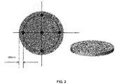
- An average flexural strength was determined by measuring the flexural strengths of the disk-shaped tungsten silicide target having a diameter of 460 mm and a thickness of 10 mm at five points as shown in FIG. 2 using a tensile compression tester (SV-201NA-50SL, from IMADA-SS Corporation) and calculating its average value.
- the Weibull Modulus was measured in accordance with the Japanese Industrial Standard defined as "JIS R 1625: 2010 Weibull statistics of strength data for fine ceramics". First, for a total of 5 points where the flexural strength was measured, plots were taken along the X axis and the Y axis in line with the following equations 1 to 3 to draw a straight line by the least squares method. The Weibull Modulus was then calculated from the slope of the straight line.
- the sputtering surface of the resulting tungsten silicide target was observed for texture image with a scanning electron microscope (JSM-7000 F from JEOL). As a result, the SEM observed texture image as shown in FIG. 3 was obtained. Subsequently, for the SEM observed texture image, the area of each Si grain was defined by using image analysis software (NIS-Element D, from Nikon Corporation). The total area S1 of the Si grains was then calculated, and the total area I1 of the Si grains having an area per a Si grain of 63.6 ⁇ m 2 or more was calculated. Subsequently, the area ratio I1/S1 (%) of I1 to S1 was calculated. Further, the average area per a Si grain in the SEM observed texture image was calculated.
- the area ratio I2/S2 (%) of I2 to S2 was then calculated. Further, the average area per a WSi 2 grain in the EBSD observed texture image (see FIG. 4(B) ) was calculated. Further, the median diameters D50 of WSi 2 grains (see FIG. 4(B) ) and the Si grains (see FIG. 4(C) ) were calculated from the EBSD analysis software, respectively.
- a tungsten silicide film was formed on a ⁇ 300 mm silicon wafer under the following sputtering conditions, and the number of particles having a size of 0.060 ⁇ m or more on the silicon wafer was measured using a particle counting device (SP 5 from KLA-Tencor) was measured. Then, the particles having a size of 0.060 ⁇ m or more mean that a diameter of the smallest circle that can surround a particle, virtually drawn on the silicon wafer, is 0.060 ⁇ m or more. The results are shown in Table 2.
- a tungsten silicide target was obtained by the same method as that of Example 1, with the exception that for the hot pressing conditions, the pressing pressure was 16.2 MPa.
- Each characteristic evaluation and sputtering test were conducted for the resulting tungsten silicide target. The results are shown in Table 2.
- a tungsten silicide target was obtained by the same method as that of Example 1, with the exception that commercially available W powder (a BET value: 0.15 to 0.20 m 2 /g) and Si powder (a BET value: 1.8 to 2.0 m 2 /g) were prepared as raw material powders as shown in Table 1, and that for the hot pressing conditions, the pressing pressure was 16.2 MPa.
- W powder a BET value: 0.15 to 0.20 m 2 /g
- Si powder a BET value: 1.8 to 2.0 m 2 /g
- a tungsten silicide target was obtained by the same method as that of Example 1, with the exception that commercially available W powder (a BET value: 0.15 to 0.20 m 2 /g) and Si powder (a BET value: 1.8 to 2.0 m 2 /g) were prepared as raw material powders as shown in Table 1. Each characteristic evaluation and sputtering test were conducted for the resulting tungsten silicide target. The results are shown in Table 2.
- a tungsten silicide target was obtained by the same method as that of Example 1, with the exception that commercially available W powder (a BET value: 0.15 to 0.20 m 2 /g) and Si powder (a BET value: 1.8 to 2.0 m 2 /g) were prepared as raw material powders as shown in Table 1, and that for the hot pressing conditions, the pressing pressure was 16.2 MPa.
- W powder a BET value: 0.15 to 0.20 m 2 /g
- Si powder a BET value: 1.8 to 2.0 m 2 /g
- a tungsten silicide target was obtained by the same method as that of Comparative Example 1, with the exception that the mixed powder of the WSi 2 powder and the Si powder obtained by the silicide synthesis was further subjected to a deoxidation heat treatment as shown in Table 1. Each characteristic evaluation and sputtering test were conducted for the resulting tungsten silicide target. The results are shown in Table 2.
- a tungsten silicide target was obtained by the same method as that of Comparative Example 1, with the exception that the sintered body obtained by hot pressing was subjected to hot isostatic pressing (HIP; a temperature rising atmosphere: an argon atmosphere, a pressure: 150 MPa, a maintaining temperature: 1370° C, a retention time: 2 hours) to re-sinter it, as shown in Table 1.
- HIP hot isostatic pressing
- a temperature rising atmosphere an argon atmosphere
- a pressure 150 MPa
- a maintaining temperature 1370° C
- retention time 2 hours
- Example 1 Raw Material Powder Pulverized Grain Deoxidation Heat Treatment Pressing Pressure [Mpa] Si/W Atomic Ratio W Powder BET Value [m 2 /g] Si Powder BET Value [m 2 /g] BET Value [m 2 /g] Oxygen Concentration [ppm by mass]
- Example 1 2.7 0.75-0.85 1.8-2.0 0.7-0.8 1700-2500 No 29.4
- Example 2 2.7 0.75-0.85 1.8-2.0 0.7-0.8 1700-2500 No 16.2
- Example 3 2.7 0.15-0.20 1.8-2.0 0.6-0.7 1500-2300 No 16.2
- Example 4 2.7 0.15-0.20 1.8-2.0 0.5-0.6 700-1300 No 29.4 Comparative Example 1 2.7 0.15-0.20 1.8-2.0 0.5-0.6 700-1300 No 16.2 Comparative Example 2 2.7 0.15-0.20 1.8-2.0 0.6-0.7 200-300 Yes 16.2 Comparative Example 3 2.7 0.15-0.20 1.8-2.0 0.2-0.3 1500-2300 No 16.
- the tungsten silicide target obtained in Examples 1 to 4 could efficiently decrease the particles during sputtering by controlling the composition of WSi x , the area of the Si grains, and the Weibull Modulus of the flexural strength, respectively.
- the WSi 2 grains on the sputtering surface of the tungsten silicide target obtained in Examples 1 to 2 substantially no WSi 2 grain having the area of 63.6 ⁇ m 2 or more was observed (0.1% or less), and the average area of the Si grains was also lower (less than 2.5 ⁇ m 2 ). Therefore, it was confirmed that these tungsten silicide target could more efficiently decrease the number of particles.
Landscapes
- Chemical & Material Sciences (AREA)
- Engineering & Computer Science (AREA)
- Organic Chemistry (AREA)
- Mechanical Engineering (AREA)
- Materials Engineering (AREA)
- Metallurgy (AREA)
- Chemical Kinetics & Catalysis (AREA)
- Plasma & Fusion (AREA)
- Physics & Mathematics (AREA)
- Analytical Chemistry (AREA)
- General Chemical & Material Sciences (AREA)
- Inorganic Chemistry (AREA)
- Manufacturing & Machinery (AREA)
- Physical Vapour Deposition (AREA)
- Inorganic Compounds Of Heavy Metals (AREA)
- Silicon Compounds (AREA)
- Electrodes Of Semiconductors (AREA)
Applications Claiming Priority (2)
| Application Number | Priority Date | Filing Date | Title |
|---|---|---|---|
| JP2018068855 | 2018-03-30 | ||
| PCT/JP2018/043048 WO2019187329A1 (ja) | 2018-03-30 | 2018-11-21 | タングステンシリサイドターゲット部材及びその製造方法、並びにタングステンシリサイド膜の製造方法 |
Publications (2)
| Publication Number | Publication Date |
|---|---|
| EP3778985A1 true EP3778985A1 (de) | 2021-02-17 |
| EP3778985A4 EP3778985A4 (de) | 2021-06-09 |
Family
ID=68061153
Family Applications (1)
| Application Number | Title | Priority Date | Filing Date |
|---|---|---|---|
| EP18912672.5A Pending EP3778985A4 (de) | 2018-03-30 | 2018-11-21 | Wolframsilicid-zielelement und verfahren zu seiner herstellung sowie verfahren zur herstellung einer wolframsilicidschicht |
Country Status (9)
| Country | Link |
|---|---|
| US (2) | US12404580B2 (de) |
| EP (1) | EP3778985A4 (de) |
| JP (2) | JPWO2019187329A1 (de) |
| KR (3) | KR20200135436A (de) |
| CN (1) | CN111971413B (de) |
| IL (1) | IL277610B2 (de) |
| SG (1) | SG11202009098QA (de) |
| TW (1) | TWI678426B (de) |
| WO (1) | WO2019187329A1 (de) |
Families Citing this family (5)
| Publication number | Priority date | Publication date | Assignee | Title |
|---|---|---|---|---|
| JP7293787B2 (ja) * | 2019-03-26 | 2023-06-20 | 株式会社プロテリアル | TaWSiターゲットおよびその製造方法 |
| JP7831285B2 (ja) * | 2020-05-26 | 2026-03-17 | 東ソー株式会社 | 金属-Si系粉末、その製造方法、並びに金属-Si系焼結体、スパッタリングターゲット及び金属-Si系薄膜の製造方法 |
| CN113817983B (zh) * | 2021-11-24 | 2022-03-18 | 武汉中维创发工业研究院有限公司 | 黑色纳米复合材料及其制备方法和应用 |
| CN114293158B (zh) * | 2021-12-13 | 2023-09-05 | 先导薄膜材料(安徽)有限公司 | 一种钨硅合金靶材的制备方法 |
| CN116356265A (zh) * | 2023-03-27 | 2023-06-30 | 有研亿金新材料(山东)有限公司 | 一种大尺寸细晶钨硅合金靶材制备方法 |
Family Cites Families (19)
| Publication number | Priority date | Publication date | Assignee | Title |
|---|---|---|---|---|
| JPH05214523A (ja) * | 1992-02-05 | 1993-08-24 | Toshiba Corp | スパッタリングターゲットおよびその製造方法 |
| JPH0616412A (ja) * | 1992-06-26 | 1994-01-25 | Mitsubishi Materials Corp | 高融点金属シリサイドの製造方法 |
| JPH06200367A (ja) * | 1992-12-28 | 1994-07-19 | Japan Energy Corp | スパッタリング用金属シリサイドターゲット |
| US5415829A (en) * | 1992-12-28 | 1995-05-16 | Nikko Kyodo Co., Ltd. | Sputtering target |
| US5464520A (en) | 1993-03-19 | 1995-11-07 | Japan Energy Corporation | Silicide targets for sputtering and method of manufacturing the same |
| JP2794382B2 (ja) * | 1993-05-07 | 1998-09-03 | 株式会社ジャパンエナジー | スパッタリング用シリサイドターゲット及びその製造方法 |
| US6309593B1 (en) * | 1993-07-27 | 2001-10-30 | Kabushiki Kaisha Toshiba | Refractory metal silicide target, method of manufacturing the target, refractory metal silicide thin film, and semiconductor device |
| JP2896233B2 (ja) * | 1993-07-27 | 1999-05-31 | 株式会社東芝 | 高融点金属シリサイドターゲット,その製造方法,高融点金属シリサイド薄膜および半導体装置 |
| JP3528980B2 (ja) * | 1994-08-03 | 2004-05-24 | 日立金属株式会社 | タングステンシリサイドターゲット材およびその製造方法 |
| JPH0820863A (ja) * | 1995-06-12 | 1996-01-23 | Toshiba Corp | シリサイド膜およびその膜を使用した半導体装置 |
| JPH09228034A (ja) | 1996-02-21 | 1997-09-02 | Mitsubishi Materials Corp | スパッタリング用タングステンシリサイドターゲットの製造方法 |
| US5919321A (en) * | 1996-08-13 | 1999-07-06 | Hitachi Metals, Ltd. | Target material of metal silicide |
| WO1999019102A1 (en) | 1997-10-14 | 1999-04-22 | Tosoh Smd, Inc. | Sputter targets and methods of making same |
| JPH11200024A (ja) | 1998-01-19 | 1999-07-27 | Nec Corp | スパッタリングターゲットおよびその製造方法 |
| JP5019343B2 (ja) * | 2004-01-27 | 2012-09-05 | Jx日鉱日石金属株式会社 | スパッタリングターゲット用ZnS粉末及びスパッタリングターゲット |
| JP5237557B2 (ja) | 2007-01-05 | 2013-07-17 | 出光興産株式会社 | スパッタリングターゲット及びその製造方法 |
| US20140363942A1 (en) * | 2013-06-11 | 2014-12-11 | Intermolecular Inc. | Method for forming a low resistivity tungsten silicide layer for metal gate stack applications |
| KR101945145B1 (ko) * | 2016-03-14 | 2019-02-01 | 제이엑스금속주식회사 | 산화물 소결체 |
| JP6768575B2 (ja) * | 2017-03-24 | 2020-10-14 | Jx金属株式会社 | タングステンシリサイドターゲット及びその製造方法 |
-
2018
- 2018-11-21 JP JP2020509611A patent/JPWO2019187329A1/ja active Pending
- 2018-11-21 IL IL277610A patent/IL277610B2/en unknown
- 2018-11-21 KR KR1020207030080A patent/KR20200135436A/ko not_active Ceased
- 2018-11-21 US US16/982,125 patent/US12404580B2/en active Active
- 2018-11-21 SG SG11202009098QA patent/SG11202009098QA/en unknown
- 2018-11-21 KR KR1020247034029A patent/KR102853073B1/ko active Active
- 2018-11-21 CN CN201880091653.1A patent/CN111971413B/zh active Active
- 2018-11-21 KR KR1020237013860A patent/KR102718697B1/ko active Active
- 2018-11-21 WO PCT/JP2018/043048 patent/WO2019187329A1/ja not_active Ceased
- 2018-11-21 EP EP18912672.5A patent/EP3778985A4/de active Pending
-
2019
- 2019-03-12 TW TW108108291A patent/TWI678426B/zh active
-
2022
- 2022-04-08 JP JP2022064767A patent/JP7269407B2/ja active Active
-
2025
- 2025-07-17 US US19/272,420 patent/US20250361599A1/en active Pending
Also Published As
| Publication number | Publication date |
|---|---|
| US20250361599A1 (en) | 2025-11-27 |
| IL277610B1 (en) | 2023-12-01 |
| KR20240155356A (ko) | 2024-10-28 |
| KR102853073B1 (ko) | 2025-09-03 |
| TW201942402A (zh) | 2019-11-01 |
| US20210025049A1 (en) | 2021-01-28 |
| KR102718697B1 (ko) | 2024-10-21 |
| US12404580B2 (en) | 2025-09-02 |
| EP3778985A4 (de) | 2021-06-09 |
| KR20200135436A (ko) | 2020-12-02 |
| TWI678426B (zh) | 2019-12-01 |
| IL277610A (en) | 2020-11-30 |
| KR20230062880A (ko) | 2023-05-09 |
| JPWO2019187329A1 (ja) | 2021-02-12 |
| WO2019187329A1 (ja) | 2019-10-03 |
| JP2022082780A (ja) | 2022-06-02 |
| CN111971413A (zh) | 2020-11-20 |
| IL277610B2 (en) | 2024-04-01 |
| CN111971413B (zh) | 2023-04-04 |
| JP7269407B2 (ja) | 2023-05-08 |
| KR102853073B9 (ko) | 2025-09-12 |
| SG11202009098QA (en) | 2020-10-29 |
Similar Documents
| Publication | Publication Date | Title |
|---|---|---|
| US20250361599A1 (en) | Tungsten silicide target and method for manufacturing same, and method for manufacturing tungsten silicide film | |
| EP3608438B1 (de) | Wolframsilizid-target und verfahren zur herstellung davon | |
| CN103797153B (zh) | Mo-W靶材及其制造方法 | |
| EP3124647B1 (de) | Sputtertarget mit al-te-cu-zr-legierung und verfahren zur herstellung davon | |
| JP4634567B2 (ja) | タングステンスパッタリングターゲットの製造方法 | |
| EP3418422B1 (de) | Ti-nb-legierung-sputtertarget und verfahren zur herstellung davon | |
| CN101287858B (zh) | 高纯度Ru合金靶及其制造方法以及溅射膜 | |
| WO2023153264A1 (ja) | Co-Cr-Pt-B系強磁性体スパッタリングターゲット | |
| US20250305112A1 (en) | Tungsten target and method for manufacturing same | |
| EP4671408A1 (de) | Sputtertarget und verfahren zur herstellung davon | |
| EP3170916B1 (de) | Sputtertarget mit al-te-cu-zr-legierung und verfahren zur herstellung davon |
Legal Events
| Date | Code | Title | Description |
|---|---|---|---|
| STAA | Information on the status of an ep patent application or granted ep patent |
Free format text: STATUS: THE INTERNATIONAL PUBLICATION HAS BEEN MADE |
|
| PUAI | Public reference made under article 153(3) epc to a published international application that has entered the european phase |
Free format text: ORIGINAL CODE: 0009012 |
|
| STAA | Information on the status of an ep patent application or granted ep patent |
Free format text: STATUS: REQUEST FOR EXAMINATION WAS MADE |
|
| 17P | Request for examination filed |
Effective date: 20201015 |
|
| AK | Designated contracting states |
Kind code of ref document: A1 Designated state(s): AL AT BE BG CH CY CZ DE DK EE ES FI FR GB GR HR HU IE IS IT LI LT LU LV MC MK MT NL NO PL PT RO RS SE SI SK SM TR |
|
| AX | Request for extension of the european patent |
Extension state: BA ME |
|
| A4 | Supplementary search report drawn up and despatched |
Effective date: 20210510 |
|
| RIC1 | Information provided on ipc code assigned before grant |
Ipc: C23C 14/34 20060101AFI20210503BHEP Ipc: C23C 14/06 20060101ALI20210503BHEP Ipc: B22F 1/00 20060101ALI20210503BHEP Ipc: B22F 3/15 20060101ALI20210503BHEP Ipc: H01J 37/34 20060101ALI20210503BHEP Ipc: B22F 9/04 20060101ALI20210503BHEP Ipc: C01B 33/06 20060101ALI20210503BHEP Ipc: C22C 29/18 20060101ALI20210503BHEP Ipc: C23C 16/442 20060101ALI20210503BHEP Ipc: C23C 16/44 20060101ALI20210503BHEP Ipc: C23C 16/513 20060101ALI20210503BHEP |
|
| DAV | Request for validation of the european patent (deleted) | ||
| DAX | Request for extension of the european patent (deleted) |