EP3779476A1 - Circuit de mesure de capacité, et dispositif de mesure de déplacement de capacité - Google Patents
Circuit de mesure de capacité, et dispositif de mesure de déplacement de capacité Download PDFInfo
- Publication number
- EP3779476A1 EP3779476A1 EP19800167.9A EP19800167A EP3779476A1 EP 3779476 A1 EP3779476 A1 EP 3779476A1 EP 19800167 A EP19800167 A EP 19800167A EP 3779476 A1 EP3779476 A1 EP 3779476A1
- Authority
- EP
- European Patent Office
- Prior art keywords
- capacitance
- conductor
- electrode
- detection means
- signal
- Prior art date
- Legal status (The legal status is an assumption and is not a legal conclusion. Google has not performed a legal analysis and makes no representation as to the accuracy of the status listed.)
- Granted
Links
Images





































Classifications
-
- G—PHYSICS
- G01—MEASURING; TESTING
- G01B—MEASURING LENGTH, THICKNESS OR SIMILAR LINEAR DIMENSIONS; MEASURING ANGLES; MEASURING AREAS; MEASURING IRREGULARITIES OF SURFACES OR CONTOURS
- G01B7/00—Measuring arrangements characterised by the use of electric or magnetic techniques
- G01B7/02—Measuring arrangements characterised by the use of electric or magnetic techniques for measuring length, width or thickness
- G01B7/023—Measuring arrangements characterised by the use of electric or magnetic techniques for measuring length, width or thickness for measuring distance between sensor and object
-
- G—PHYSICS
- G01—MEASURING; TESTING
- G01R—MEASURING ELECTRIC VARIABLES; MEASURING MAGNETIC VARIABLES
- G01R27/00—Arrangements for measuring resistance, reactance, impedance, or electric characteristics derived therefrom
- G01R27/02—Measuring real or complex resistance, reactance, impedance, or other two-pole characteristics derived therefrom, e.g. time constant
- G01R27/26—Measuring inductance or capacitance; Measuring quality factor, e.g. by using the resonance method; Measuring loss factor; Measuring dielectric constants ; Measuring impedance or related variables
- G01R27/2605—Measuring capacitance
-
- G—PHYSICS
- G01—MEASURING; TESTING
- G01B—MEASURING LENGTH, THICKNESS OR SIMILAR LINEAR DIMENSIONS; MEASURING ANGLES; MEASURING AREAS; MEASURING IRREGULARITIES OF SURFACES OR CONTOURS
- G01B7/00—Measuring arrangements characterised by the use of electric or magnetic techniques
- G01B7/02—Measuring arrangements characterised by the use of electric or magnetic techniques for measuring length, width or thickness
-
- G—PHYSICS
- G01—MEASURING; TESTING
- G01D—MEASURING NOT SPECIALLY ADAPTED FOR A SPECIFIC VARIABLE; ARRANGEMENTS FOR MEASURING TWO OR MORE VARIABLES NOT COVERED IN A SINGLE OTHER SUBCLASS; TARIFF METERING APPARATUS; MEASURING OR TESTING NOT OTHERWISE PROVIDED FOR
- G01D5/00—Mechanical means for transferring the output of a sensing member; Means for converting the output of a sensing member to another variable where the form or nature of the sensing member does not constrain the means for converting; Transducers not specially adapted for a specific variable
- G01D5/12—Mechanical means for transferring the output of a sensing member; Means for converting the output of a sensing member to another variable where the form or nature of the sensing member does not constrain the means for converting; Transducers not specially adapted for a specific variable using electric or magnetic means
- G01D5/14—Mechanical means for transferring the output of a sensing member; Means for converting the output of a sensing member to another variable where the form or nature of the sensing member does not constrain the means for converting; Transducers not specially adapted for a specific variable using electric or magnetic means influencing the magnitude of a current or voltage
- G01D5/24—Mechanical means for transferring the output of a sensing member; Means for converting the output of a sensing member to another variable where the form or nature of the sensing member does not constrain the means for converting; Transducers not specially adapted for a specific variable using electric or magnetic means influencing the magnitude of a current or voltage by varying capacitance
-
- G—PHYSICS
- G01—MEASURING; TESTING
- G01D—MEASURING NOT SPECIALLY ADAPTED FOR A SPECIFIC VARIABLE; ARRANGEMENTS FOR MEASURING TWO OR MORE VARIABLES NOT COVERED IN A SINGLE OTHER SUBCLASS; TARIFF METERING APPARATUS; MEASURING OR TESTING NOT OTHERWISE PROVIDED FOR
- G01D5/00—Mechanical means for transferring the output of a sensing member; Means for converting the output of a sensing member to another variable where the form or nature of the sensing member does not constrain the means for converting; Transducers not specially adapted for a specific variable
- G01D5/12—Mechanical means for transferring the output of a sensing member; Means for converting the output of a sensing member to another variable where the form or nature of the sensing member does not constrain the means for converting; Transducers not specially adapted for a specific variable using electric or magnetic means
- G01D5/14—Mechanical means for transferring the output of a sensing member; Means for converting the output of a sensing member to another variable where the form or nature of the sensing member does not constrain the means for converting; Transducers not specially adapted for a specific variable using electric or magnetic means influencing the magnitude of a current or voltage
- G01D5/24—Mechanical means for transferring the output of a sensing member; Means for converting the output of a sensing member to another variable where the form or nature of the sensing member does not constrain the means for converting; Transducers not specially adapted for a specific variable using electric or magnetic means influencing the magnitude of a current or voltage by varying capacitance
- G01D5/241—Mechanical means for transferring the output of a sensing member; Means for converting the output of a sensing member to another variable where the form or nature of the sensing member does not constrain the means for converting; Transducers not specially adapted for a specific variable using electric or magnetic means influencing the magnitude of a current or voltage by varying capacitance by relative movement of capacitor electrodes
- G01D5/2417—Mechanical means for transferring the output of a sensing member; Means for converting the output of a sensing member to another variable where the form or nature of the sensing member does not constrain the means for converting; Transducers not specially adapted for a specific variable using electric or magnetic means influencing the magnitude of a current or voltage by varying capacitance by relative movement of capacitor electrodes by varying separation
Definitions
- a displacement meter As one of means for measuring the distance to an object or the like, a displacement meter is used. As major non-contact displacement meters, laser displacement meters, eddy current displacement meters, and an electrostatic capacitive displacement meters are commonly used, and thus, features of the laser displacement meter, the eddy current displacement meter, and the electrostatic capacitive displacement meter are compared first.
- the object detection A method for detecting an object affecting an electrostatic capacitance is hereinafter referred to as "the object detection".
- an output of the drive signal generating means 201 is directly connected to an inverting input of the amplifier U of the signal detection means 501.
- an output impedance of the drive signal generating means 201 is low, an input allowable voltage of the amplifier U of the signal detection means 501 may be exceeded, and a failure of the amplifier U may be caused.
- an unillustrated protective element or an appropriate protection circuit may be additionally connected to an input of the amplifier U of the signal detection means 501.
- a drive signal amplitude is defined as Vin
- a drive signal frequency is defined as f
- an output amplitude of signal detection means 501 is defined as Vout.
- an impedance of the inter electrode capacitance Cx is 1/(2 ⁇ f ⁇ Cx)
- an impedance of the feedback capacitance Cf is 1/(2 ⁇ f ⁇ Cf)
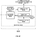
- the measuring means 601 includes output means and outputs pieces of information on various measurement results such as the output amplitude Vout of the signal detection means 501, the inter electrode capacitance Cx, the inter electrode distance and the object state and results obtained by performing determinations by appropriate means.
- the output means widely includes displaying and printing of various pieces of information (including printing and graph output of values), an alarm indicating an abnormality or the like found by determination, and a contact output, but is not limited to these.
- the measuring means 601 may include communication means to transmit the pieces of information to necessary places via the communication means. Details of the measuring means are described in a nineteenth embodiment described later.
- the inter electrode capacitance Cx can be known based on the output amplitude Vout of the signal detection means 501.
- the inter electrode distance and the inter electrode capacitance Cx are in an inversely proportional relationship, and thus, the inter electrode distance can be known by knowing the inter electrode capacitance Cx.
- the inter electrode distance can be known from the inter electrode capacitance Cx.
- the inter electrode distance and the inter electrode capacitance Cx are in a certain functional relationship, and thus, by knowing the inter electrode capacitance Cx, the inter electrode distance can be known.
- the use of the CM circuit 101 enables the object detection that affects the inter electrode capacitance Cx, and the object in this case does not need to be a conductor. For example, if an object having a larger dielectric constant than air is provided between the drive electrode 301 and the detection electrode 401, the inter electrode capacitance Cx increases, and thus, it is possible to know an amount, a thickness and the like of a dielectric based on the degree of increase.
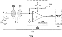
- a CM circuit 102 includes signal detection means 502 instead of signal detection means 501.
- the signal detection means 502 includes the previously described amplifier U and negative feedback unit 702.
- the negative feedback unit 702 includes the previously described feedback capacitance Cf and a discharge switch Sf that is connected in parallel to the feedback capacitance Cf. When the discharge switch Sf is turned on, the feedback capacitance Cf is discharged and a voltage across terminals of the negative feedback unit 702 becomes zero. As a result, an output of the amplifier U included in the signal detection means 502 comes to have the same potential as an inverting input.
- the third embodiment shows another example of suppressing an instability of a DC component of an output of signal detection means and an output saturation.
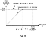
- Fig. 3A to Fig. 3C illustrate one example of a CM circuit, a frequency characteristic, an output noise characteristic according to the third embodiment and
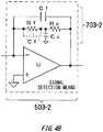
- Fig. 4A to Fig. 4D illustrate a modified example of signal detection means of the CM circuit according to the third embodiment.
- the same reference numerals are denoted to the same parts as Fig. 1 and Fig. 2 . Descriptions of a part that is the same as that of either the first embodiment or the second embodiment is omitted.
- a CM circuit 103 includes signal detection means 503 instead of the signal detection means 501, 502.
- the signal detection means 503 includes the previously described amplifier U and negative feedback unit 703.
- the negative feedback unit 703 includes the previously described feedback capacitance Cf and a feedback resistance Rf that is connected in parallel to the feedback capacitance Cf.
- the feedback resistance Rf is one example of a first feedback resistance and is a resistance for discharging.
- the thermal noise at the drive signal frequency is reduced to 1/10 because the frequency corresponding to the time constant becomes 1/100 and the thermal noise beome 10 times. That is, noise of the signal detection means 503 caused by the feedback resistance Rf can be reduced if the feedback resistance Rf is large.
- the inter-terminal capacitance Cf is present in an actual resistive element used as the feedback resistance Rf and is connected in parallel to the feedback resistance Rf and the feedback capacitance Cf.
- an inter-terminal capacitance of a chip resistance is about 0.1 pF, and thus, the feedback capacitance Cf is usable if the feedback capacitance Cf is large enough to be not affected by the capacitance (as one example, when feedback capacitance Cf is 1 pF or more).
- the inter-terminal capacitance Cf of an actual resistive element has a lower Q-factor (quality factor) than an actual capacitative element, varies largely in a capacitance, and its capacitance value is not guaranteed, and thus, the inter-terminal capacitance Cf may cause a performance degradation of the signal detection means 503.
- a gain of a buffer amplifier is lower than one, an attenuation factor of an attenuator by the resistance R1 and the resistance R2 may be decreased by the gain for compensation.
- an attenuation factor of an attenuator may be increased by the gain.
- the fourth embodiment shows another example of suppressing an instability of a DC component of an output of signal detection means and an output saturation.
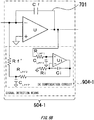
- Fig. 5A illustrates one example of a CM circuit according to the fourth embodiment and
- Fig. 5B illustrates one example of signal detection means of a CM circuit.
- the same reference numerals are denoted to the same parts as Fig. 1 , Fig. 2 and Fig. 3A . Descriptions of the same parts as those in any of the first embodiment to the third embodiment are omitted.
- a filter is not limited to this, and a high-order low-pass filter, an LC filter and the like are freely selectable.
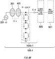
- a CM circuit 105 of Fig. 6A includes a noise elimination circuit 1005 provided between a detection electrode 401 and signal detection means 505.
- the noise elimination circuit 1005 includes a parallel bandpass filter (P-BPF) (hereinafter referred to as "parallel BPF") and a capacitance Cd and is provided between the detection electrode 401 and the signal detection means 505.
- P-BPF parallel bandpass filter
- the parallel BPF is one example of a first resonance circuit and a bandpass filter by a parallel resonance circuit.
- the parallel resonance circuit is formed of, for example, a parallel resonant capacitor Cpp and a parallel resonant inductor Lpp.
- a resonance frequency of the parallel BPF is matched to a drive signal frequency.
- an AC signal of a drive signal frequency generated in drive signal generating means 201 is not attenuated because an impedance becomes high at a resonance frequency and an impedance becomes infinite for a parallel resonance circuit using an ideal element.
- an impedance becomes low at a frequency other than a resonance frequency, and thus, for example, a hum of a utility frequency, external noise due to an electromagnetic wave and the like can be attenuated, and accordingly, the parallel BPF can operate as a bandpass filter.
- a bandpass filter may be a higher-order bandpass filter by a method of adding a parallel BPF between a detection electrode 401 and a series BPF or between a series BPF and an input of signal detection means 505 or alternately having a plurality of parallel BPFs and a plurality of series BPFs. (When a parallel BPF is provided immediately before an input of signal detection means 505, the above described capacitance Cd is necessary.)
- a CM circuit 105-4 of Fig. 8C includes a noise elimination circuit 1005-4 instead of the noise elimination circuit 1005.
- the noise elimination circuit 1005-4 includes a parallel band elimination filter (P-BEF) (hereinafter referred to as "parallel BEF").
- the parallel BEF is one example of a second resonance circuit, is a band elimination filter based on a parallel resonance circuit, and is provided between a detection electrode 401 and signal detection means 505.
- the parallel resonance circuit includes, for example, a parallel resonance capacitor Cpe and a parallel resonance inductor Lpe. A resonance frequency of the parallel resonance circuit is matched to a frequency of a hum or external noise to be removed.
- the parallel BEF In the parallel BEF, an impedance becomes high at a resonance frequency (impedance becomes infinite for a parallel resonance circuit using an ideal element), and thus, a frequency component to be removed is unlikely to be transmitted to signal detection means 505. On the other hand, in the parallel BEF, at a frequency other than a resonance frequency, an impedance becomes low, and thus, a frequency component of a drive signal frequency is not attenuated and is transmitted to signal detection means 505. As a result, the parallel BEF operates as a band elimination filter for attenuating only a hum or external noise.
- the series BEF and the parallel BEF can be used in combination.
- a resonance frequency or passing and attenuation characteristics change due to a mutual influence.
- the parallel BPF and the series BEF are used in parallel, two pass frequencies and a single attenuation frequency there between appear.
- desired passing and attenuation characteristics can be obtained, and thus, exemplifications of further combinations are omitted.
- a CM circuit 106 of Fig. 9A according to the sixth embodiment is unlikely to receive an influence of a hum and external noise by having a grounded shield electrode 1106 in the vicinity of a detection electrode 401 and having a shielding wire 1206 that has a grounded outer conductor and is used for connection to signal detection means 506.
- Either one of a shield electrode 1106 and a shielding wire 1206 may be used or as illustrated in Fig. 9A , each of the shield electrode 1106 and the shielding wire 1206 may be independently grounded for use, and the shield electrode 1106 and the shielding wire 1206 are hereinafter collectively referred to as "shield".
- An expression "grounding" of the shield electrode 1106 and the shielding wire 1206 indicates an AC-ground, and may include a DC voltage. (The same applies hereinafter.)
- a technique of the present disclosure has a feature of not being affected by a stray capacitance between the detection electrode 401 and a ground.
- An electrostatic capacitance between the detection electrode 401 and the shield electrode 1106 and an electrostatic capacitance of the shielding wire 1206 can be considered as one type of a stray capacitance, and thus, in the sixth embodiment, an influence of an electrostatic capacitance by a shield is not received.
- An impedance becomes high at a drive signal frequency by using the electrostatic capacitance as a parallel BPF, and thus, an influence of the electrostatic capacitance is further reduced.
- a stray capacitance appears to be 1/Av of an actual capacitance.
- An influence of a stray capacitance due to a shield can be significantly reduced even when a real buffer amplifier B is used although a stray capacitance does not seem to become zero completely because a gain of the real buffer amplifier B is slightly smaller than one and a slight delay is caused.
- the parallel BPF according to the fifth embodiment illustrated in Fig. 6A may be used.
- a capacitance between a detection electrode 401 and a shield is not used for a resonance circuit, such configuration can be used in combination with an active shield.
- all of a series connection of resonance circuits of parallel BPFs according to the fifth embodiment as in Fig. 6B , the series BPF as in the Fig. 8A , the series BEF as in Fig. 8B , and the parallel BEF as in Fig. 8C can be used in combination with an active shield.
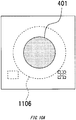
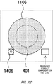
- a printed circuit board may be used as one example of a more specific method of realizing the detection electrode 401 and the shield electrode 1106, a printed circuit board may be used.
- Fig. 10A to Fig. 10C illustrate one example of using a printed circuit board as a detection electrode and a shield electrode. In Fig. 10A to Fig. 10C , illustration of a wiring pattern or the like is omitted.
- the printed circuit board 1306 may be used as the drive electrode 301.
- an output impedance of drive signal generating means 201 is high, it is likely that a hum or external noise enters the drive electrode 301, but this can be prevented by providing the shield electrode 1106 on a surface opposite to the drive electrode 301 of the printed circuit board 1306 and grounding it.
- the detection electrode 401 is realized by the printed circuit board 1306, signal detection means 506 or the like can be implemented on the printed circuit board 1306 and further, measuring means 601 or the like can be implemented on the printed circuit board 1306.
- the drive electrode 301 is realized by the printed circuit board 1306, drive signal generating means 201 or the like can be implemented on the printed circuit board 1306.
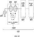
- the seventh embodiment shows an example of detecting by a resonance circuit that an inter electrode capacitance Cx is a specific value.
- Fig. 11A to Fig. 12B illustrate one example of a CM circuit according to the seventh embodiment.
- the same reference numerals are denoted to the same parts as those in Fig. 1 , Fig. 2 , Fig. 3A , Fig. 5A and Fig. 5B . Descriptions of the same parts as those in any of the first embodiment to the fourth embodiment are omitted.
- Signal detection means 507 may be any of the signal detection means previously described in the first embodiment to the fourth embodiment.
- the inter electrode capacitance Cx changes depending on an inter electrode distance in the case of distance measurement or an object state affecting the inter electrode capacitance Cx in the case of the object detection, and thus, a resonance frequency of a parallel resonance circuit 1507 changes accordingly.
- the drive signal frequency is constant.
- an output amplitude Vout of signal detection means 507 is proportional to an inter electrode capacitance Cx.
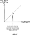
- the parallel resonance circuit 1507 according to the seventh embodiment if a capacitance becomes a specific inter electrode capacitance Cx such that the resonance frequency matches the drive signal frequency, the AC current from the drive electrode 301 to the detection electrode 401 hardly flows. As a result, the output amplitude Vout of the signal detection means 507 decreases, and thus, a "dip" as shown in a graph of Fig. 11B occurs.
- a horizontal axis represents an inter electrode capacitance Cx and a vertical axis represents an output amplitude Vout of signal detection means 507.
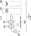
- a CM circuit 107-1 according to the seventh embodiment of Fig. 12A includes a series resonant inductor Ls' provided between a detection electrode 401 and signal detection means 507.
- the series resonant inductor Ls' is connected in series with the inter electrode capacitance Cx to configure a series resonant circuit 1607.
- a resonance frequency of the series resonant circuit 1607 changes by change in the inter electrode capacitance Cx, and if the resonance frequency is matched to the drive signal frequency, an impedance of the series resonant circuit 1607 becomes low and an AC current from the drive electrode 301 to the detection electrode 401 easily flows.
- a resonance frequency of the series resonant circuit 1607 does not match the drive signal frequency, the AC current from the drive electrode 301 to the detection electrode 401 is hardly affected and an AC current proportional to the inter electrode capacitance Cx flows.
- an inter electrode distance becomes a specific distance in the case of distance measurement or an object affecting an inter electrode capacitance Cx is in a specific state in the case of the object detection
- a peak occurs in the output amplitude Vout of the signal detection means 507.
- an output amplitude Vout of signal detection means 507 is arranged to be maximum by adjusting a distance between a detection electrode 401 that is an object and a drive electrode 301 that is an object, adjusting an interval between objects to a specific distance becomes possible.
- an unillustrated resistance is connected to any one or more positons between the drive signal generating means 201 and the drive electrode 301, between the detection electrode 401 and the series resonant inductor Ls', and between the series resonant inductor Ls' and the signal detection means 507, an effect of reducing the sharpness of the peak can be obtained.
- a relationship between the inter electrode capacitance Cx at a frequency away from the resonance frequency and the output amplitude Vout of the signal detection means 507 deviates from Equation 1 due to an influence of a resistance, but a correction can be performed.
- a direct current resistance of the series resonant inductor Ls' has the same effect as such resistance.
- Fig. 12A illustrates an example of providing the series resonant inductor Ls' between the detection electrode 401 and the signal detection means 507
- the same effect can be obtained even if the series resonant inductor Ls' is provided between the drive signal generating means 201 and the drive electrode 301.
- inductors are provided both between the detection electrode 401 and the signal detection means 507 and between the drive signal generating means 201 and the drive electrode 301, a sum of the inductances operate as an inductance of the series resonant inductor Ls'.
- the eighth embodiment shows an example of using an amplifier configured by a discrete device as an amplifier U included in signal detection means.
- the eighth embodiment can be configured as similarly to the first embodiment to the seventh embodiment except that an amplifier configured by a discrete device is used as an amplifier U.
- the illustration of a CM circuit and descriptions on devices other than an amplifier configured by a discrete device are omitted.
- a sufficient ("deep”) phase compensation is applied to a commercially available operational amplifier IC such that the amplifier IC does not oscillate even in various negative feedback circuits and the amplifier IC has a feature of a differential input.
- an amplifier configured by a discrete device can be designed so as to be optimal for a feedback capacitance Cf actually used and to be applied with (“shallow") phase compensation, and accordingly, a broadband of the amplifier is possible.
- a broadband of an amplifier is also possible by using a high speed discrete device or designing a circuit configuration and an operation point. If a broadband amplifier can be used, an open-loop gain of an amplifier at a drive signal frequency increases, and thus, an influence of a stray capacitance can be reduced more reliably.
- an input of an amplifier configured by a discrete device By setting an input of an amplifier configured by a discrete device to be a single input amplifier instead of the differential input amplifier, noise can be reduced and an amplifier having a high S/N ratio can be realized.
- the single input amplifier can reduce noise caused at an input stage to 1 / 2 compared to the differential input amplifier.
- DC potentials between an input and an output differ and a potential difference may change depending on an ambient temperature or a power supply voltage.
- DC compensation circuits 904, 904-1 of the fourth embodiment can correct an influence of a potential difference.
- the signal detection means of the eighth embodiment can also be applied to signal detection means of other embodiments.
- a generally available actual capacitative element is, as one example, a minimum of 0.1 pF and contains a problem that as a capacitance is smaller, a relative error is larger.
- An error of an actual capacitative element of 0.1 pF is relatively large, as one example, ⁇ 0.05 pF, that is ⁇ 50%.
- an element of an absolute error of the same ⁇ 0.05pF is available, and thus, if, for example, 1 pF can be used, an error is ⁇ 5%, and if 5pF is used, an error is sufficiently relatively small, such as ⁇ 1%.
- Equation 3 an equivalent feedback capacitance Cf is expressed as the following Equation 4.
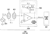
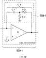
- an amplifier operates as similar to when the buffer amplifier B having a gain of one is present even if the buffer amplifier B is absent. That is, in such a case, the same effect can be obtained by the signal detection means 509-1 in Fig. 13B . If a gain of the buffer amplifier B is smaller than one, an attenuation factor of an attenuator is decreased by that amount, and if a gain is larger than one, an attenuation factor of an attenuator is increase by that amount, and accordingly, the same effect can be obtained.
- an impedance of the feedback capacitance Cf when the drive signal frequency is 318 kHz is about 200 k ⁇ . If the resistance R3 is 24k ⁇ and the resistance R4 is 1k ⁇ , a parallel resistance value of the resistances R3 and R4 is 0.96 k ⁇ , which is sufficiently smaller than about 200k ⁇ .
- an equivalent feedback capacitance Cf of 0.1 pF having a small relative error can be obtained by the feedback capacitance Cf of 2.5pF having a small relative error.
- sensitivities of signal detection means 501 to 507 of CM circuits 101 to 107 may need to be switched over a wide range. If sensitivities are switched by switching feedback capacitances Cf of signal detection means 501 to 507, an influence of a stray capacitance of the switching circuit is received, and thus, particularly, switching of feedback capacitances Cf having small capacitances may often be difficult.
- the ninth embodiment it is only necessary to switch at least one of the resistance R3 or the resistance R4, and thus, sensitivities can be switched easily. Switching is also possible by using the ninth embodiment for the feedback capacitance Cf having a small capacitance or using a capacitative element as it is for the feedback capacitance Cf having a larger capacitance.
- the tenth embodiment shows an example of achieving high sensitivity by adding an amplifier circuit for amplifying an output of signal detection means.
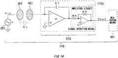
- Fig. 14 illustrates one example of a CM circuit according to a tenth embodiment.
- the same reference numerals are denoted to the same parts as those in Fig. 1 , Fig. 2 , Fig. 3A , Fig. 5A and Fig. 5B . Descriptions of the same parts as those in any of the first embodiment to the fourth embodiment are omitted.
- a CM circuit 110 includes signal detection means 510 having an amplifier circuit 1710. An input of the amplifier circuit 1710 is connected to an output of an amplifier U included in the signal detection means 510 and an output of the amplifier circuit 1710 is connected to measuring means 601. By adding the amplifier circuit 1710, a CM circuit 110 with higher sensitivity can be realized.
- an amplification factor of an added amplifier circuit 1710 is defined as A
- an output amplitude of an amplifier U included in the signal detection means 510 is defined as Vout'
- an output amplitude of the signal detection means 510 is defined as Vout
- the highly sensitive signal detection means 510 with an amplification factor A can be realized.
- phase-detection means when phase-detection means is used, a polarity of an output voltage of the phase-detection means is inverted by a phase inversion, and thus, the means may be applied by considering this.
- An amplifier circuit 1710 to be added is sufficient if it is an amplifier circuit that can amplify a necessary frequency component in an output signal of an amplifier U included in the signal detection means 510, a non-inverting amplifier circuit using an operational amplifier and an amplifier circuit of other circuit types are widely applicable.
- an amplifier circuit 1710 to be added is an amplifier circuit that can also amplify a direct current
- a DC offset voltage is multiplied by an amplification factor A, and thus, the error may become large or the amplifier circuit 1710 may be saturated.
- a capacitative element may be added to an input side of an amplifier circuit 1710 to be added for capacitive coupling.
- sensitivities can be switched by switching an amplification factor A of an amplifier circuit 1710 to be added, and thus, sensitivities can be switched easily by switching resistances.
- the tenth embodiment can be freely combined with other embodiments for use and can be freely combined with the ninth embodiment having an effect of high sensitivity for application.
- a CM circuit 111 in Fig. 15 includes a changeover switch SW and a reference capacitance Cr.
- the changeover switch SW is one example of switching means, is provide behind drive signal generating means 201, and a drive signal is connected to a common contact of the changeover switch SW.
- the changeover switch SW has one contact connected to a drive electrode 301 and the other contact connected to one terminal of a reference capacitance Cr. That is, the changeover switch SW is arranged between the drive signal generating means 201, and the drive electrode 301 and the reference capacitance Cr and connects the drive signal generating means 201 to the drive electrode 301 or the reference capacitance Cr in a switchable manner.
- the attenuator AT can be insert between the other contact and the reference capacitance Cr.
- the other terminal of the reference capacitance Cr is connected to the detection electrode 401 and the input of the signal detection means 511. That is, the reference capacitance Cr is connected between the other contact of the changeover switch and an input of the signal detection means.
- the changeover switch SW in the case where the output of the drive signal generating means 201 is connected to the reference capacitance Cr via the attenuator AT, the output amplitude Vout of the signal detection means 511 becomes 1.0 Vrms by applying 0.1 pF (attenuation factor of attenuator AT ⁇ reference capacity Cr) to Equation 1 instead of the inter electrode capacitance Cx of Equation 1.
- the output amplitude Vout of the signal detection means 511 changes accordingly. For example, in the above example, if the feedback capacitance Cf changes to 0.9 pF, the output amplitude Vout of the signal detection means 511 changes to 0.99 Vrms and 0.9 Vrms accordingly.
- a ratio 1.1 Vrms to 1.0 Vrms that is 1.1 and a ratio of 0.99 Vrms to 0.9 Vrms that is 1.1 are kept constant. That is, the inter electrode capacitance Cx can be accurately known based on the output amplitude Vout of the signal detection means 511 when the attenuation factor of the attenuator AT and the reference capacitance Cr are selected.
- the attenuation factor of the attenuator AT is preferably selected such that differences in the output amplitude Vout of the signal detection means when the changeover switch is switched are small.
- a timing at which the changeover switch SW is switched to the reference capacitance Cr side is arbitrary.
- the changeover switch SW can be switched during the movement of an object. Switching at a timing at which a calibration based on the reference capacitance is necessary is possible and for example, during a time period after turning on a power source until when a circuit operation or an ambient temperature is stabilized, switching may be performed frequently and after stabilization , switch frequency may be lowered. Switching may be performed periodically.
- the eleventh embodiment may be freely combined with other embodiments for use.
- the above described seventh embodiment contains a portion where a proportional relationship between the inter electrode capacitance Cx and the output amplitude Vout of the signal detection means does not hold, and thus, there is a case where it is inappropriate to combine the embodiment for use.
- the above described fifth embodiment shows an example of reducing an influence of noise and the like by providing noise elimination circuits 1005, 1005-1, 1005-2, 1005-3, and 1005-4 including a resonance circuit between the detection electrode 401 and the signal detection means 505 when the capacitance measurement is performed based on a single frequency (sine wave).
- the twelfth embodiment achieves the same effect by providing the filter at the input side of the measuring means.
- any filter is applicable as long as it can reduce an influence of noise and the like.
- a digital filter by performing an A/D conversion.
- an active filter it is also possible to cause a filter circuit to have a gain to be used also as the amplifier circuit 1710 of the tenth embodiment.
- a bandpass filter that allows only a drive signal frequency to be passed
- a band elimination filter that removes a frequency of noise and the like
- LPF low-pass filter
- HPF high-pass filter
- a necessary frequency component extracted by the filter fc is provided to AC amplitude measurement means AC that measures an AC amplitude based on various methods described in a section of a measuring circuit in the above described first embodiment.
- AC signal measurement means AC various methods described in a section of the measuring means in the first embodiment can be used.
- the comparison determination means described in a section of a measuring circuit in the above described first embodiment can use the thus obtained AC amplitude information for the determination of the measurement result.
- the twelfth embodiment can be freely combined with other embodiments for use.
- the thirteenth embodiment shows an example of using phase-detection means as measuring means. According to the phase-detection means, it is possible to extract only a drive signal frequency component and further know a phase.
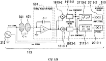
- Fig. 17A to Fig. 17C illustrate one example of a CM circuit according to the thirteenth embodiment.
- the same reference numerals are denoted to the same parts as those in Fig. 1 , Fig. 2 , Fig. 3A , Fig. 5A and Fig. 5B . Descriptions of the same parts as those in any of the first embodiment to the fourth embodiment are omitted.
- examples of a drive electrode 301, a detection electrode 401, and signal detection means 501 are the same as those in the above described first embodiment ( Fig. 1 ), those in other embodiments can be used as appropriate.
- the phase-detection means 1813-1 has one input, provided with, for example, the sin signal as a reference signal and the other input connected to the output of the signal detection means 501.
- the phase-detection means 1813-2 has one input provided with, for example, the cos signal as a reference signal and the other input connected to the output of the signal detection means 501.
- the phase-detection means 1813-1 and 1813-2 are, for example, phase detectors.
- a 90 degrees phase shift circuit may be used in combination. If a direct digital synthesizer (DDS) is used as drive signal generating means 213, it is expected to obtain two signals having a more accurate 90 degrees phase difference, and thus, details thereof are described in the eighteenth embodiment later.
- DDS direct digital synthesizer
- the phase-detection means 1813-1 and 1813-2 multiply two inputs.
- the phase-detection means 1813-1 has an output connected to averaging means 1913-1 and the phase-detection means 1813-2 has an output connected to averaging means 1913-2.
- the phase-detection means extracts only a frequency component of a reference signal frequency and has an effect of removing a frequency component of a frequency other than a reference signal frequency (for example, a hum or noise).
- a DC voltage Y proportional to a sin component from output signals of the signal detection means 501 can be obtained and from outputs of the phase-detection means provided with a cos signal as a reference signal-averaging means, a DC voltage X proportional to a cos component from output signals of the signal detection means 501 can be obtained.
- the operation means 2113-2 that performs an operation as in Equation 8 may be provided between the averaging means 1913-2 and the DC voltage measuring means 2013-2 as necessary, and the obtained DC voltages X and Y may be provided to the operation means 2113-2 so as to obtain the output amplitude Vout of the signal detection means 501.
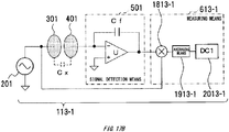
- a drive signal at a cos signal side, the phase-detection means 1813-2, the averaging means 1913-2, and the operation means 2113-1 and 2113-2 are unnecessary and a configuration like the circuit 113-1 in Fig. 17B can be adopted. That is, the averaging means 1913-1 is connected to an output of the phase-detection means 1813-1 and the DC voltage measuring means 2013-1 is connected to an output of the averaging means 1913-1.
- the averaging means 1913-1 and 1913-2 may be configured by a low-pass filter and the like when being realized in an analog fashion.
- the DC voltage measuring means 2013-1 and 2013-2 may be analog means or may use digital means by performing an A/D conversion.
- the DC voltage measuring means 2013-1 and 2013-2 may be used as means for appropriately knowing various digitally realized averaging means 1913-1 and 1913-2 and resultant digital values as DC voltage values.
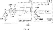
- a CM circuit 113-2 in Fig. 17C includes drive signal generating means 201 and measuring means 613-2.
- heterodyne detection means it is possible to know an inter electrode capacitance Cx by extracting a frequency component fc through a filter fc and providing the component to AC amplitude measurement means AC. Such a configuration is referred to as heterodyne detection means.
- the heterodyne detection means is one example of the phase-detection means.
- a frequency f of the drive signal generating means 201 and a frequency fh of the reference signal generator 2213 are preferably selected such that a frequency fc is lower than f and fh.
- a bandpass filter having the same configuration it is general to have the same relative bandwidth (value obtained by dividing bandwidth by center frequency), independently of the center frequency. That is, as the center frequency fc of the filter fc that is the bandpass filter is lower, the bandwidth is narrower. If a filter is selected such that the frequency fc is low, a narrow bandwidth can be realized, and thus, an effect of further improving an ability of removing an unnecessary frequency component such as noise is generated.
- the phase-detection means 1813-1, 1813-2, and 2313, the averaging means 1913-1 and 1913-2, the filter fc, the AC amplitude measurement means AC, the drive signal generating means 213 and 201, and the reference signal generator 2213 may use either an analog circuit or a digital circuit or use an analog circuit and a digital circuit in combination.
- phase-detection means 1813-1, 1813-2, and 2313 are realized by an analog circuit
- a reference signal may be a sine wave for example and an analog multiplier may be used as phase-detection means 1813-1, 1813-2, and 2313.
- a reference signal provided from the drive signal generating means 201 and 213 and the reference signal generator 2213 may be a square wave and the phase-detection means 1813-1, 1813-2, and 2313 with an analog circuit that switches positive/ negative of a gain by the square wave may be used.
- the averaging means 1913-1 and 1913-2 are realized by an analog circuit, a DC component may be extracted by using an appropriate low-pass filter and the extracted DC component may be provided to DC voltage measuring means 2013-1 and 2013-2.
- a direct digital synthesizer (DDS) is used as the drive signal generating means 201 and 213 and the reference signal generator 2213, a reference signal can be obtained as a digital signal and it is easy to obtain a signal having a 90 degrees phase difference.
- DDS direct digital synthesizer
- the averaging means 1913-1 and 1913-2 are realized by digital circuits, DC components may be extracted by using appropriate averaging methods such as moving average, integration by digital operation, and a low-pass filter by a digital filter and a digital value thereof may be known as a DC voltage.
- An operation may be performed by using an analog operation circuit or a digital circuit as similar to the case where an operation for knowing an amplitude and a phase is performed based on Equation 8 and Equation 9.
- a frequency characteristic of an inter electrode capacitance Cx may be measured by appropriately changing a drive signal frequency of the drive signal generating means 201 and a reference signal frequency of the reference signal generator 2213 while keeping a difference between both frequencies at a frequency fc.
- the fourteenth embodiment shows an example of simplifying some of them.
- Fig. 18A and Fig. 18B an example is illustrated in which it is sufficient that the number of detection electrodes is one and the number of signal detection means is one.
- Fig. 19 it is sufficient that the number of drive signal generating means is one and the number of drive electrode is one.
- the number of single detection electrode can be one and the number of single signal detection means can be one, and additionally the number of measuring means can be one.
- switching means is used in combination.
- Fig. 21 to Fig. 23B also use switching means in combination.
- the number of drive signal generating means can be one and the number of drive electrode can be one, and additionally the number of measuring means can be one.
- the number of drive electrode is more than one and the number of the remaining components can be one respectively.
- the number of detection electrode is more than one and the number of the remaining components may be one respectively.
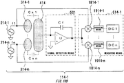
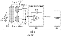
- Each of a CM circuit 114 in Fig. 18A and a CM circuit 114-1 in Fig. 18B includes drive signal generating means 214-1 ... 214-n, drive electrodes 314-1 ... 314-n and a detection electrode 414.
- Each of the drive signal generating means 214-1 ... 214-n is the same as the drive signal generating means 201 previously described in the first embodiment and each of the drive electrodes 314-1 ... 314-n is the same as the drive electrode 301 previously described in the first embodiment.
- the drive signal generating means 214-1 ... 214-n are connected to the drive electrodes 314-1 ... 314-n on a one-to-one basis respectively.
- the detection electrode 414 forms inter electrode capacitances Cx1 ...
- the CM circuit 114 includes measuring means 614 having the filters fc1 ... fcn and the AC voltage measuring means AC1 ... ACn previously described in the twelfth embodiment and the CM circuit 114-1 includes measuring means 614-1 having the phase-detection means 1814-1 ... 1814-n, the averaging means 1914-1 ... 1914-n, and the DC voltage measuring means DC1 ... DCn previously described in the thirteenth embodiment.
- a drive signal of a frequency f1 generated by the drive signal generating means 214-1 is supplied to a first drive electrode 314-1, a drive signal of an unillustrated frequency f2 is supplied to a second unillustrated drive electrode, and in the same manner, a drive signal of a frequency fn is supplied to a n-th drive electrode 314-n.
- n is an arbitrary natural number of two or more.
- Frequencies f1 to fn are different from each other and selected are frequencies separated to the extent the frequencies can be separated by the filters fc1 ... fcn and the phase-detection means 1814-1 ... 1814-n.
- a inter electrode capacitance between the detection electrode 414 and the first drive electrode 314-1 is defined as Cx1 and in the similar manner, an inter electrode capacitance between the detection electrode 414 and the n-th drive electrode 314-n is defined as Cxn.
- the n filters fc described in the twelfth embodiment are connected to an input of the measuring means 614.
- the AC voltage measuring means AC1 is connected to an output of the filter fc1 for extracting only the frequency f1
- unillustrated AC voltage measuring means AC2 is connected to the filter fc2 for extracting only an unillustrated frequency f2
- the AC voltage measuring means ACn is connected to a filter fcn for extracting only the frequency fn.
- the inter electrode capacitances Cx1 ... Cxn can be obtained based on the filters fc1 ... fcn and the AC voltage measuring means AC1 ... ACn respectively.
- measuring means using a plurality of AC voltage measuring means corresponding to respective filters is exemplified, but outputs of n filters may be switched by using one (or less than n) AC voltage measuring means.
- One (or less than n) filter that can switch frequencies to be extracted and the AC voltage measuring means may be used.
- CM circuit 114-1 an example is shown in which a plurality of averaging means and a plurality of DC voltage measuring means corresponding to respective phase-detection means are used, but one (or less than n) DC voltage measuring means may be used by switching to it, or one (or less than n) averaging means and DC voltage measuring means may be used by switching there between.
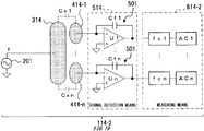
- drive signal generating means 201 generates a drive signal waveform of a frequency f and the waveform is supplied to a drive electrode 314.
- n is an arbitrary natural number of two or more.
- Each of filters fc1 ... fun and phase-detection means 1814-1 ... 1814-n extracts a frequency component of a frequency f.
- the CM circuit 114-2 includes a drive electrode 314, detection electrode 414-1 ... 414-n, signal detection means 514, and measuring means 614-2. Inter electrode capacitances Cx1 ... Cxn are formed between the drive electrode 314 and each of detection electrodes 414-1 ... 414-n.
- the signal detection means 514 includes a plurality of signal detection means 501 previously described in the first embodiment and inputs of the signal detection means 501 are connected to the detection electrodes 414-1 ... 414-n respectively on a one-to-one basis.
- Measuring means 614-2 includes filters fc1 ... fcn and AC voltage measuring means AC1 ... ACn and the filters fc1 ... fcn and the AC voltage measuring means AC1 ...
- ACn form a plurality of sets, each set including a single filter and a single AC voltage measuring means.
- the plurality of sets including the filters and the AC voltage measuring means are connected to a plurality of outputs of the signal detection means 501 on a one-to-one basis.
- a set of phase-detection means, averaging means, and DC voltage measuring means may be used instead of a set of a filter and AC voltage measuring means.
- An inter electrode capacitance between a drive electrode 314 and a first detection electrode 414-1 is defined as Cx1
- the signal detection means 514 to which the first detection electrode 414-1 is connected includes a feedback capacitance Cf1 and an amplifier U1 and supplies a frequency component of a frequency f to AC voltage measuring means AC1 via a filter fc1 for extracting the frequency component of the frequency f.
- a first to n-the components have the same configuration.
- a difference resides in that while the number of drive signal generating means 214-1 ... 214-n can be reduced from n to one, the number of amplifier U and feedback capacitance Cf included in the signal detection means 501 increases from one to n, and thus, one of them suitable for actual use can be selected.
- Fig. 20A to Fig. 23B illustrate a modified example of simplifying signal detection means and measuring means by adding a signal source and switching means.
- a CM circuit 114-3 in Fig. 20A is a modified example in which the heterodyne detection means described in the above thirteenth embodiment is configured by adding a signal source 2214 and a multiplier 2314 and accordingly the signal detection means 501 and the measuring means 614 are simplified from the CM circuit 114.
- the filter fc extracts the frequency f1 supplied to the first drive electrode 314-1. If the AC voltage measuring means AC in the measuring means 614-3 measures an amplitude of the thus selected frequency f1, the inter electrode capacitance Cx1 between the first drive electrode 314-1 and the detection electrode 414 can be informed. By switching signal source frequencies fh, each of a first inter electrode capacitance to an n-th inter electrode capacitance Cxn can be informed in the same manner.
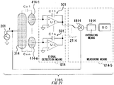
- a CM circuit 114-5 in Fig. 21 is an example obtained by simplifying the drive signal generating means 201, the drive electrode 314, and the measuring means 614-5 by adding a changeover switch 2714 that is one example of the switching means.
- a changeover switch 2714 that is one example of the switching means.
- a plurality of sets of detection electrodes and signal detection means are used, and a plurality of points are measured by switching with the changeover switch 2714 of the measuring means 614-5.
- one drive signal generating means 201 outputs only one frequency.
- the measuring means 614-5 in the CM circuit 114-5 may include only one set of the phase-detection means 1814 and the DC voltage measuring means DC.
- the CM circuit 114-5 is the same as the CM circuit 114-2 in that a plurality of sets of the detection electrodes 414-1 ... 414-n and the signal detection means 501 are used.
- the CM circuit 114-5 may include the measuring means 612 including the filter fc and the AC signal measurement means AC shown in the twelfth embodiment for example.
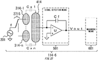
- Fig. 56A and Fig. 56B described later will illustrate a specific example of an electrostatic capacitive displacement meter applied with the CM circuit 114-6 in Fig. 22 .
- CM circuit 114-7 a plurality of detection electrodes are used, and one of the detection electrodes and the signal detection means 501 are connected by switching between the detection electrode and the signal detection means 501 with the changeover switch 2716.
- a CM circuit 114-8 in Fig. 23B is a modified example of the CM 114-7 in Fig. 23A .
- Connection of a single detection electrode and signal detection means 501 in the CM circuit 114-7 and the CM circuit 114-8 may be hereinafter abbreviated as "selection".
- detection electrodes other than selected detection electrodes among a plurality of detection electrodes are electrically floated.
- detection electrodes other than the selected detection electrodes are grounded. This allows using grounded electrodes other than the selected detection electrodes for shaping lines of electric force. (Details of the above are described as a guard electrode in a second example described later.)
- Fig. 23B only the detection electrode 414-1 is select and connected to the signal detection means 501 by changeover switch 2717-1.
- Other detection electrodes 414-2 (unillustrated) to 414-n are connected to a reference potential (grounded) via the changeover switches 2717-2 (unillustrated) to 2717-n.
- Each of the first inter electrode capacitance Cx1 to the n-th inter electrode capacitance Cxn can be known by similarly switching from the changeover switch 2717-1 to the changeover 2717-n and sequentially selecting from the detection electrodes 414-1 to 414-n.
- the CM circuits 114-3, 114-4, 114-5, 114-6, 114-7, and 114-8 are modified examples obtained by simplifying the measuring means and adding a signal source and switching means, these are merely representative examples, and the present invention is not limited to these.
- the fifteenth embodiment shows an example of measuring two points by using drive signal generating means that can generate two signals having 90 degrees phase difference and two drive electrodes corresponding to the means.
- the number of detection electrode is one
- the number of signal detection means is one
- the number of measuring means is one.
- Fig. 24 illustrates one example of a CM circuit according to the fifteenth embodiment.
- the same reference numerals are denoted to the same parts as those in Fig. 1 , Fig. 2 , Fig. 3A , Fig. 5A and Fig. 5B . Descriptions of the same parts as those in any of the first embodiment to the fourth embodiment and the thirteenth embodiment are omitted.
- CM circuit 115 as similar to the thirteenth embodiment described above, as examples of two signals having 90 degrees phase difference, a sin signal and a cos signal are exemplified, but the present invention is not limited to this as long as two signals having 90 degrees phase difference are provided in the circuit.
- a signal having 90 degrees phase difference is used.
- Signals having 90 degrees phase difference orthogonal to each other have properties of not affecting each other, and thus, two points can be measured independently.
- a relative dielectric constant may change when frequencies are different, i.e., a frequency characteristic is provided, and thus, if a plurality of frequencies are used as in Fig. 18A , Fig. 18B , Fig. 20A , and Fig. 20B according to the fourteenth embodiment, the frequency characteristic of the relative dielectric constant may become an error factor.
- the fifteenth embodiment has an advantage that a frequency characteristic of a relative dielectric constant does not become an error factor because only a single frequency is required by using a phase difference.
- Fig. 25A , Fig. 25B , Fig. 25C , and Fig. 26 illustrate an example of detecting a position of a detection electrode using a CM circuit of the present disclosure, and illustrate an example of performing the object detection for detecting a specific position.
- a circle symbol attached to an end of a lead wire of a detection electrode represents a point connected to signal detection means (unillustrated) and illustration of measuring means is omitted.
- drive signal generating means 5421 generates different drive signals having 180 degrees phase difference, the signals are applied to two drive electrodes 5422-1 and 5422-2 and the detection electrode 5423 is provided between drive electrodes 5422-1 and 5422-2 in a movable manner.
- One of drive signals is defined as 0°, a voltage thereof is defined asV0, and an inter electrode distance between a corresponding drive electrode 5422-1 and a detection electrode 5423 is defined as d 0 .
- the other drive signal is defined as 180°, a voltage thereof is defined as V 180 , and an inter electrode distance between the corresponding drive electrode 5422-2 and the detection electrode 5423 is defined as d 180 .
- the detection electrode 5423 If the detection electrode 5423 is moved and when the voltage V0 is equal to voltage V 180 , the inter electrode distance d 0 and the inter electrode distance d1 80 are equal and two drive signals cancel each other, and accordingly, an output amplitude Vout of signal detection means of a CM circuit becomes zero. That is, it is possible to know a fact that the detection electrode 5423 reaches the center of two drive electrodes 5422-1 and 5422-2.
- FIG. 25A illustrates one-dimensional position detection
- Fig. 25B and Fig. 25C illustrate two-dimensional position detection.
- Fig. 25B realizes two-dimensional position detection by providing two sets of one-dimensional position detection in Fig. 25A vertically and horizontally.
- a drive signal frequency for a vertical position detection as f1
- a drive signal frequency for a horizontal position detection as f2
- a position detection in a vertical direction can be performed based on f1
- a position detection in a horizontal direction can be performed based on f2
- three-dimensional position detection can also be realized if another set of one-dimensional position detection is added in the front-back direction and a further different frequency f3 is used.
- Fig. 25C also realizes two-dimensional position detection by providing two sets of one-dimensional position detection in Fig. 25A vertically and horizontally.
- vertical position detection is 0 degree and 180 degrees and horizontal position detection is 90 degrees and 270 degrees, and thus, the vertical and horizontal phase difference is 90 degrees.
- two-dimensional position detection can be realized with a single frequency because both vertical and horizontal position detections are possible by adopting a method as in Fig. 24 according to the fifteenth embodiment.
- Fig. 25B and Fig. 25C illustrate a cylindrical detection electrode such that both the vertical direction and the horizontal direction do not have directivities.
- a shape of a drive electrode is not limited to a planar shape, but for example four drive electrodes in arc shape of less than 90 degrees may be arranged to form an electrode shape close to a cylinder, and a shape of an electrode may be freely deformed according to an application.
- phase-detection means When using phase-detection means that uses a zero degree drive signal as a reference signal as measuring means of a CM circuit, an output of phase-detection means becomes a negative value for a 180 degrees component and the output becomes a positive value for a zero degree component. If a horizontal axis represents a position of a detection electrode present in left and right directions of a drive electrode so that positions of the electrode correspond to the horizontal axis, an output voltage of phase-detection means that uses zero degree drive signal as a reference signal is represented by a solid line in a graph 2603 in Fig. 26 .
- an output voltage of phase-detection means that uses a zero degree drive signal as a reference signal has an error with respect to a solid line in a graph 2603 in Fig. 26 .
- supplied to rectangular electrodes respectively are a 90 degrees drive signal and a 270 degrees drive signal having 90 degrees phase difference relative to drive signals supplied to an electrode 2601 and an electrode 2602 having right triangle shapes.
- an elongate detection electrode is parallel to a drive electrode plane in a high direction, that is, when a height Z1 and a height Z2 in a figure are equal, a 90 degrees drive signal and a 270 degrees drive signal cancel each other, and as a result, an output voltage of signal detection means that uses a 90 degrees drive signal as a reference signal becomes zero.
- an output voltage of phase-detection means that uses a 90 degrees drive signal as a reference signal becomes a positive or negative value, and thus, an angle of a detection electrode is corrected such that the output voltage becomes zero.
- an output voltage of phase-detection means that uses a 0 degree drive signal as a reference signal changes as in a graph 2603 in Fig. 26 .
- a drive signal having a phase difference of every 90 degrees is used and the phase-detection means separates and measures 0 degree drive signal/180 degrees drive signal and a 90 degrees drive signal/270 degrees drive signal
- the present invention is not limited to this.
- a pair of drive signals may have a different frequency from a pair of 0 degree and 180 degrees and have a phase difference of 180 degrees.
- a 90 degrees drive signal side and a 270 degrees drive signal side in Fig. 26 if different frequencies are used respectively, it is possible to know highs Z1 and Z2 independently.
- one of rectangular electrodes and a drive signal corresponding thereto can be omitted.
- both rectangle electrodes and drive signals thereof can be omitted.
- the seventeenth embodiment shows an application example of obtaining a DC voltage proportional to one of capacitances and inversely proportional to the other capacitance.
- Fig. 27 illustrates one example of a CM circuit according to the seventeenth embodiment.
- the same reference numerals are denoted to the same parts as those in Fig. 1 , Fig. 2 , Fig. 3A , Fig. 5A and Fig. 5B . Descriptions of the same parts as those in any of the first embodiment to the fourth embodiment are omitted.
- the proportional side capacitance When as the proportional side capacitance, the reference capacitance is used and the inversely proportional side capacitance is measured as the inter electrode capacitance, a DC voltage inversely proportional to an inter electrode capacitance can be obtained.
- an influence of an edge effect of a parallel plate is small, an inter electrode capacitance is substantially inversely proportional to an inter electrode distance, and thus, a DC voltage substantially proportional to an inter electrode distance can be obtained.
- Drive signal generating means 216 generates a square wave of an amplitude of ⁇ V1 at a drive electrode and is connected to an input of signal detection means 501 via a capacitance C1 that is one example of a first capacitance.
- the drive signal generating means 216 further generates a changeover switch signal synchronized with a square wave and switches and drives a switch 2816 and a switch 3016.
- phase-detection means in measuring means 616 of the seventeenth embodiment is one example of first phase-detection means, phase-detection means using such analog circuit is exemplified, and the above described changeover switch signal is a reference signal to switch positive/ negative of a gain.
- a triangle symbol "-1" in the phase-detection means 1816 represents an inverting amplifier circuit having a gain of one time and an output of an inverting amplifier is supplied to one of contacts of a switch 2816 in the phase-detection means 1816.
- a non-inverting amplifier circuit having a gain of one time may be used when necessary. If an inverting amplifier circuit having a gain absolute value larger than one and a non-inverting amplifier circuit having the same gain absolute value are used, high sensitivity similar to that in the above described tenth embodiment can be realized.
- An output of the phase-detection means 1816, that is a common contact of the switch 2816 is connected to an input of an integrating circuit.
- the integrating circuit is one example of averaging means, includes an amplifier Ui', an integrator resistance Ri', and an integral capacity Ci', and converts an output of the phase-detection means 1816 into a direct current. This DC voltage is V2.
- the switch 3016 is switched and driven by the above described changeover switch signal and operates such that when a voltage of a drive electrode is +V1, a contact of a switch of a DC voltage-V2 side and a common contact are connected and when a voltage of a drive electrode is -V1, a contact of a switch of a DC voltage V2 side and a common contact are connected.
- the common contact of the switch is connected to an input of the signal detection means 501 via a capacitance C2 that is one example of a second capacitance.
- a circuit in Fig. 27 operates so as to satisfy Equation 11 below.
- V 1 ⁇ C 1 V 2 ⁇ C 2
- Equation 12 can be obtained by modifying Equation 11. [Math 8] V 2 ⁇ V 1 C 1 C 2
- a capacitative element that makes C2 a reference capacitance is used and C1 is operated as an inter electrode capacitance, as similar to the above described embodiments, a DC voltage V2 proportional to the inter electrode capacitance C1 can be obtained.
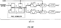
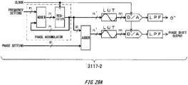
- the eighteenth embodiment shows an example of using DDS as drive signal generating means. That is, the embodiment shows an example of using drive signal generating means including DDS.
- Fig. 28A and Fig. 28B illustrate one example of DDS according to the eighteenth embodiment.
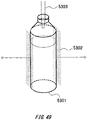
- a relationship between an inter electrode capacitance Cx of a drive electrode and a detection electrode and a capacitance of liquid in a container and a liquid level is known in advance and the relationship is approximated by a function, and at the time of an actual measurement, an electrostatic capacitive displacement meter can be realized in which an accurate capacitance of liquid in a container can be known by applying the measured capacitance to the approximate function.
- distance measurement and the object detection at a plurality of locations are possible by providing either a plurality of drive electrodes or a plurality of detection electrodes.
- a capacitance between the diaphragm 5003 and the fixed electrode 5007 changes by being almost inversely proportional to an inter electrode distance between the diaphragm 5003 and the fixed electrode 5007, and thus, a measurement target pressure can be known from a capacitance.
- the diaphragm 5003 may correspond to either a drive electrode or a detection electrode and also the fixed electrode 5007 may correspond to either a drive electrode or a detection electrode vice versa.
- a relationship between a capacitance between the diaphragm 5003 and the fixed electrode 5007 and a measurement target pressure is measured in advance and the relationship is approximated by an appropriate function, and accordingly, a more accurate measurement target pressure can be known.
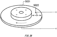
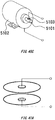
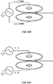
- Fig. 38 illustrates an example of testing a surface deflection, an surface asperity, a flatness and the like (hereinafter referred to as "surface deflection and the like") of a brake disc of an automobile or the like (hereinafter referred to as "disc”).
- the disc 5021 (object) is rotatable, can be a drive electrode or a detection electrode, and is for example, provided horizontally.
- a moving electrode 5022 is provided at a position slightly away from the disc 5021 and can be moved in parallel to the disc 5021 in a diameter direction of the disc 5021.
- a detection electrode can be made relatively small by causing a larger disc 5021 (object) to be a drive electrode and a smaller moving electrode 5022 to be a detection electrode.
- An influence of a hum or ambient noise can be reduced by, providing a shield electrode to a surface opposite from the disc 5021 in a detection electrode or using shielding wire for wiring between a detection electrode and signal detection means.
- the disc 5021 is a detection electrode and a moving electrode 5022 is a drive electrode, there is an advantage of suppressing a radiation wave radiated from a drive electrode because the drive electrode is small.
- a drive electrode and a detection electrode can be selected appropriately by considering shapes or the like of an object and an electrode in this manner. The same applies to other examples described later. In examples described later, more preferable combinations may be shown, but the present invention is not limited to the shown combination.
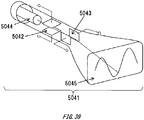
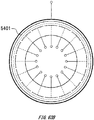
- Fig. 39 illustrates an example of performing the distance measurement between deflection plates of the CRT 5041.
- a broken line indicates a trajectory of an electron beam.
- An electron beam emitted from an electron gun 5044 deflects in a vertical direction by a voltage between vertical deflection plates 5042, deflects left and right directions by a voltage between horizontal deflection plates 5043, and then reaches a phosphor screen 5045.
- a horizontal axis can be set to a time axis by applying a saw-tooth wave to a horizontal deflection plate 5043 and a vertical axis can be set to an input voltage axis by amplifying an input voltage waveform and applying the amplified waveform to a vertical deflection plate 5042.
- a voltage waveform of an X input can be amplified and the amplified waveform can be applied to the horizontal deflection plate 5043 and a voltage waveform of a Y input can be amplified and the amplified waveform can be applied to a vertical deflection plate 5042.
- Two vertical deflection plates 5042 (both of which are objects) have the same shape, and thus, it is free to determine which is a drive electrode and which is a detection electrode. The same applies to two horizontal deflection plates 5043 (both of which are objects).
- electrostatic capacitive displacement meter of a prior art, one needs to be a dedicated electrode and the other needs to be a grounded conductor, and thus, the electrostatic capacitive displacement meter may not be applied to an application as in this example.
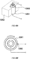
- Fig. 40A illustrates an example of performing the distance measurement between electrodes of a dry battery.
- the distance measurement is performed by pressing a dry battery 5061 against a positioning gauge 5062 for fixing, setting a lower electrode of the dry battery 5061 to be, for example, a drive electrode, setting an electrode 5063 fixed at a position slightly away from an upper part of the dry battery 5061 to be a detection electrode, and measuring a capacitance between an upper electrode of the dry battery 5061 and the electrode 5063.
- Fig. 40B illustrates an example of measuring a roundness of a bearing
- an axis of a metal bearing 5081 object
- the other electrode 5082 is fixed slightly outside the bearing 5081. If the bearing 5081 has a complete roundness, an inter electrode capacitance does not change even if the bearing 5081 is rotated. If an inter electrode capacitance changes depending on a rotation of the bearing 5081, it is possible to know a change in the inter electrode distance therefrom, and accordingly, a roundness of the bearing 5081 can be known.
- a distance measurement using a set of a drive electrode and a detection electrode can be used to other various applications, and thus, those are listed below.
- the second example and Fig. 41A to Fig. 43D illustrate specific application examples of performing the distance measurement between two places by using two drive electrodes or two detection electrodes in specific examples of performing the distance measurement by using the electrostatic capacitive displacement meter of the present disclosure.
- Fig. 41A illustrates an example in which one of two conductors is set to be a drive electrode and the other conductor is set to be a detection electrode, is a reference example included in the first example, and is outside the scope of the second example.
- an inter electrode distance between an electrode positioned between two conductors and each conductor is measured based on a method of using two drive signals having 90 degrees phase differences as show in the fifteenth embodiment described above.
- a sin signal as a drive signal is given to one conductor
- a cos signal as a drive signal is given to the other conductor
- an inter electrode distance between each of two conductors and an electrode can be known by phase-detection means as described in the fifteenth embodiment.
- a distance between two conductors can be known by (an inter electrode distance between one conductor and an electrode+an inter electrode distance between the other conductor and an electrode+a thickness of an electrode).
- an inter electrode distance between an electrode positioned between two conductors and each conductor is measured individually based on the method of using a plurality of (two) frequencies as shown in Fig. 18A and Fig. 18B of the fourteenth embodiment described above.
- a drive signal having a frequency f1 is given to one conductor
- a drive signal having a frequency f2 is given to the other conductor
- two drive electrodes are provided. This allows knowing an inter electrode distance between each of two conductors and an electrode as described in the fourteenth embodiment.
- a distance between two conductors can be known by (an inter electrode distance between one conductor and an electrode+an inter electrode distance between the other conductor and an electrode+a thickness of an electrode).
- a method of using a plurality of frequencies will be described in the third example described later by using a further specific example.
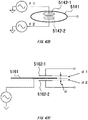
- FIG. 41D an inter electrode distance between an electrode positioned between two conductors and each conductor is measured individually based on a method shown in Fig. 19 as in the fourteenth embodiment described above and a method of using switching as shown in Fig. 21 , Fig. 23A and Fig. 23B .
- Fig. 19 illustrates an example of using filters fc1 ... fcn and AC voltage measuring means AC1 ... ACn, phase-detection means, averaging means, and DC voltage measuring means can be used as measuring means.
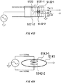
- a thickness of a conductor 5161 is measured by measuring an inter electrode distance between one conductor 5161 and two detection electrodes 5162-1 and 5162-2 respectively based on a method illustrated in Fig. 19 of the fourteenth embodiment described above.
- a rotation state of the turntable 5181 is viewed from the side when a squareness of the metal part 5182 is not complete (that is, slightly declined) and the center of the metal part matches with the center of the turntable 5181 (that is, there is no misalignment), the metal part 5182 moves as indicated by vertical solid line and broken line of the metal part 5182 as illustrated in Fig. 43B .
- a capacitance between a drive electrode of a sin signal side and the metal part 5182 is defined as Csin and a capacitance between a drive electrode of a cos signal side and the metal part 5182 is defined as Ccos.
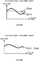
- the metal part 5182 When the metal part 5182 is inclined without having the misalignment in Fig. 43A and Fig. 43B , the metal part changes as illustrated in Fig. 43C in which a horizontal axis represents a rotation angle of the turntable 5181 and a vertical axis represents a capacitance Csin of a sin signal side and a capacitance Ccos of a cos signal side.
- the squareness of the metal part 5182 can be known from a difference in a capacitance change between the capacitance Csin and the capacitance Ccos.
- a method of using two drive signals having a 90 degrees phase difference, a method of using a plurality of (two) frequencies, and a method illustrated in Fig. 19 of the fourteenth embodiment described above are described as specific examples, but the present invention is not limited to these.
- an electrostatic capacitive displacement meter according to an application and a requirement performance may be realized by appropriately using heterodyne detection means and switching means described in the fourteenth embodiment for example.
- the third example and Fig. 44 to Fig. 47 illustrate a specific example of performing the distance measurement of three places or more in the distance measurement by the electrostatic capacitive displacement meter of the present disclosure.
- Fig. 44 illustrates an example of measuring an inclination angle and a vertical position of a metallic plate 5201
- Fig. 45 illustrates an example of measuring a stress strain of an automotive door
- Fig. 46 illustrates an example of measuring a roundness based on a 3-point method.
- the heterodyne detection means and the switching means can be appropriately used.
- a distance between the electrode A and the electrode B is known, and thus, an inclination a can be known if the distance A and the distance B are informed.
- the metallic plate is inclined in a downward arrow direction of a in Fig. 44 .
- a distance between the electrode C and the center between the electrode A and the electrode B is known, and thus, an inclination ⁇ can be known if the distances A, B, and C are informed.
- an average value of the distance A and the distance B>the distance C it can be known that the metallic plate is inclined in an upward arrow direction of ⁇ in Fig. 44 .
- a vertical position Z can be known. For example, if an average value of the distances A, B, and C is smaller than a reference value, it is possible to know that the metallic plate 5201 is raised in an arrow direction of Z in Fig. 44 .
- Fig. 45 illustrates an example of measuring a stress strain of an automotive door by the distance measurement of more than three places.
- the automotive door 5221 (object) is one of the drive electrode/detection electrode.
- the other of the drive electrode/detection electrode is a plurality of electrodes 5223 provided to a jig 5222 for electrode positioning.
- Fig. 47 illustrates an example of measuring a squareness, a parallelism, and a size of a steel plate.
- one of drive electrode/detection electrode is a square steel plate 5261 (object) itself and the other of the drive electrode/detection electrode is electrodes 5262-1, 5262-2, 5262-3, 5262-4, 5262-5, and 5262-6 provided in the vicinity of the steel plate 5261.
- a position of the steel plate 5261 is determined by a positioning guide 5263.
- Inter electrode distances between electrodes 5262-1, 5262-2, 5262-3, 5262-4, 5262-5, and 5262-6 and the steel plate 5261 are respectively referred to as a first distance, a second distance, a third distance, a fourth distance, a fifth distance and a sixth distance.
- the first distance to the sixth distance are measured individually by using a master steel plate having an accurate squareness and size. At this time, electrode positions may be adjusted such that inter electrode distances of respective electrodes 5262-1, 5262-2, 5262-3, 5262-4, 5262-5, and 5262-6 become the same. Next, the first distance to the sixth distance are measured individually by using the steel plate 5261 of an object.
- An inclination of a steel plate side surface of a side of an electrode 5262-1 and an electrode 5262-2 can be known by knowing a difference between the first distance and the second distance, and an inclination of a steel plate side surface of a side of an electrode 5262-3 and an electrode 5262-4 can be known by knowing a difference between the third distance and the fourth distance.
- a lower size of the steel plate 5261 (width in Fig. 47 ) can be known from the first distance and the third distance and an upper size of the steel plate 5261 can be known from the second distance and the fourth distance.
- a size in the vicinity of the center of the steel plate 5261 can be estimated also based on (an average value of the first distance and the second distance) and (an average value of the third distance and the fourth distance.)
- the parallelism between a lower surface and an upper surface of the steel plate 5261 can be known by knowing a difference between the fifth distance and the sixth distance.
- a size in the vicinity of a left side surface of the steel plate 5261 (vertical width in Fig. 47 ) can be known from the fifth distance
- a size in the vicinity of a right side surface can be known from the sixth distance
- a size in the vicinity of the center of the steel plate 5261 in the left and right directions can be known from an average value of the fifth distance and the sixth distance.
- the fourth example and Fig. 48 to Fig. 53B illustrate a specific example when a set of drive electrodes and detection electrodes is used in the object detection by the electrostatic capacitive displacement meter of the present disclosure.
- a specific example illustrated in each figure is merely a representative example, and in the case of using a set of drive electrodes and detection electrodes also, the object detection by the electrostatic capacitive displacement meter of the present disclosure can be applied to a wide range of applications.
- Fig. 48 illustrates an example of measuring a thickness of a tape like object such as a tape or a belt (hereinafter referred to as "tape") 5281 on a production line.
- a tape 5281 is sent in an arrow direction via rollers 5282 and sets of drive electrodes and detection electrodes 5283 are provided so as to sandwich the tape 5281 in a non-contact manner.
- the tape 5281 has a larger relative dielectric constant than air, and thus, an inter electrode capacitance Cx becomes larger than when there is no tape 5281 and the inter electrode capacitance Cx increases as the tape 5281 is thicker. Since an inter electrode distance is constant, the inter electrode capacitance Cx does not change even if the tape 5281 is moved in a vertical direction in the figure, and thus, a thickness of the tape 5281 can be known from the inter electrode capacitance Cx.
- a thickness of the tape 5281 is normal (inter electrode capacitance Cx is between minimum value and maximum value), whether the tape 5281 is too thick (inter electrode capacitance Cx is maximum value or above), and whether the tape 5281 is too thin (inter electrode capacitance Cx is minimum value or less) by performing two comparisons, in Fig. 48 , i.e., a comparison between the measured inter electrode capacitance Cx and an upper limit value of a thickness of the tape 5281 (maximum value of inter electrode capacitance Cx) and a comparison between the measured inter electrode capacitance Cx and a lower limit value of a thickness of the tape 5281 (minimum value of inter electrode capacitance Cx).
- Fig. 48 illustrates an example of measuring a thickness of a tape like object having a small width by using a set of drive electrodes and detection electrodes.
- a set of drive electrodes and detection electrodes is applicable in the case where it is sufficient if a thickness of the object at a specific position is knows and when a width and an average thickness of an entire surface are known.
- a set of drive electrodes and detection electrodes is applicable to, for example, a paper feeding mechanism that detects that papers are fed in an overlapping manner at a specific position.
- Fig. 49 illustrates an example of measuring an amount of liquid injected to a liquid container.
- Sets of drive electrodes and detection electrodes 5302 are provided to side surfaces of the liquid container 5301 as illustrated in the figure.
- a relative dielectric constant of liquid injected in the liquid container 5301 or a container is larger than a relative dielectric constant of air.
- an inter electrode capacitance Cx become the smallest when the liquid container 5301 is not present between electrodes, becomes a little large when the empty liquid container 5301 is present, and becomes the largest when the maximum amount liquid is filled. This allows knowing an amount of liquid in the liquid container 5301 from the inter electrode capacitance Cx.
- An inter electrode capacitance increases slightly if, for example, the liquid container 5301 fed by a belt conveyor is stopped between electrodes, and accordingly, it can be detected that the liquid container 5301 is stopped at a predetermined position.
- a nozzle 5303 comes down from an upper part of a container and an injection of liquid is started, as the liquid increases, an inter electrode capacitance Cx increases.
- a capacitance reaches an inter electrode capacitance Cx corresponding to a predetermined amount of liquid, an injection of liquid is terminated, the nozzle 5303 is pulled upward, and then, the container is changed to a next liquid container 5301.
- a threshold for determine the presence or absence of the liquid container 5301 can be compared with a threshold corresponding to a predetermined amount of liquid.
- a difference in an electrostatic capacitance due to an individual difference such as a thickness of the liquid container 5301 itself is in in unnegligible level
- an electrostatic capacitance when the liquid container 5301 is empty as a reference value it can be known that an amount of liquid reaches a predetermined amount from an increase in an electrostatic capacitance.
- Fig. 49 illustrates an example of providing sets of drive electrodes and detection electrodes 5302 that are planar electrodes to both side surfaces of the liquid container 5301, the more high sensitivity can be achieved by using electrode curved along the liquid container 5301.
- the liquid container 5301 is positioned by moving curved electrodes to sandwich the liquid container 5301, and accordingly a variation in the measurement can be reduced.
- a nozzle 5303 may be passed through a hole provided to an electrode of an inlet side of a container.
- individual inter electrode capacitances in a plurality of frequencies can be obtained by the object detection using a set of drive electrodes and detection electrodes and based on the capacitances, a frequency characteristic such as a dielectric constant of an object can be known.
- drive signal generating means 201 generates a drive signal including a plurality of frequency components.
- a frequency superposition waveform can be used.
- a square wave, a saw-tooth wave, and a triangular wave having a plurality of harmonic components can be used, and these waveforms can be easily generated by a commonly used technique. (Although it is possible to use a waveform having more frequency components such as white noise and pink noise, since a frequency component of each waveform is small, an S/N ratio may not be expected that much.)
- Measuring means 620 is configured to be able to know each of a plurality of frequencies required.
- the measuring means 620 may have a configuration similar to that of measuring means 614 in Fig. 18A according to the fourteenth embodiment and measuring means 614-3 in Fig. 20A .
- frequency characteristics of n points of fl ... fn can be known.
- a frequency characteristic for a necessary frequency component of a fundamental wave and a harmonic can be known.
- a frequency superposition waveform is likely to have a larger amplitude than a sine wave of a single frequency and an output of an amplifier of signal detection means is more likely to be saturated.
- individual frequencies to be superimposed may be selected appropriately, phases of individual frequency components to be superimposed may be adjusted respectively, and an adjustment may be made such that a peak voltage of a frequency superposition waveform becomes minimum or becomes small as much as necessary.
- frequencies to be superimposed are known in advance, each phase through which a peak voltage becomes small can be obtained by calculation or simulation.
- Fig. 50A and Fig. 50B illustrate, as one example, an example when sine waves of 1kHz and 3kHz are superimposed.
- Fig. 50A illustrates the case where a phase of 3kHz (thin solid line) is 180 degrees when a phase of 1kHz (dotted line) is 0 degree.
- a peak value of the frequency superposition waveform in this case is twice a peak value of a sine wave of 1kHz or a sine wave of 3kHz.
- Fig. 50B illustrates the case where a phase of 3kHz (thin solid line) is also 0 degree when a phase of 1kHz (dotted line) is 0 degree.
- a peak value of the frequency superposition waveform (thick solid line) of this case is about 1.54 times a sine wave of 1kHz or 3kHz. That is, in this case, a peak voltage can be reduced to nearly 80% by selecting phases of frequency components to be superimposed.
- drive signal generating means 213 in Fig. 17A or drive signal generating means 201 in Fig. 17B or Fig. 17C frequencies to be measured are sequentially generated (frequencies are swept).
- measuring means 620 measuring means 613 in Fig. 17A , measuring means 613-1 in Fig. 17B , and measuring means 613-2 in Fig. 17C are used individually.
- For configurations, operations, features and the like of the means in Fig. 17A to Fig. 17C please refer to relevant parts of descriptions in the fourteenth embodiment and further descriptions are omitted here.
- Fig. 51A to Fig. 52B illustrate an example of instructing a device to perform some sort of operations by moving a part of a human body (a finger is illustrated) close to/away from between electrodes and an example of using the electrostatic capacitive displacement meter of the present disclosure as a proximity sensor.
- Fig. 51A is a perspective view showing an example of a positional relationship between an electrode and a finger guard
- Fig. 51B is a front view illustrating an example of a positional relationship between an electrode and a finger guard and also illustrates moving close/moving away state of a finger.
- a finger guard has functions to restrict a movable range of a finger and to prevent a finger from directly touching an electrode.
- Fig. 52A and Fig. 52B illustrate examples of output voltages of the electrostatic capacitive displacement meter of the present disclosure when a finger is moved close or away in Fig. 51A and Fig. 51B .
- a human body behaves like a grounded conductor, and thus, if a finger is moved close to an electrode, an inter electrode capacitance decreases, and if a finger is moved away from an electrode, a state of an inter electrode capacitance returns to an original state.
- Fig. 52A illustrates examples of patterns of moving close/away a finger in Fig. 51A and Fig. 51B and examples of output voltages of the electrostatic capacitive displacement meter of the present disclosure corresponding to individual patterns.
- a lower right middle part indicates a state where slow moving close and fast moving away are continuously generated and a lower right end part indicates an output voltage when stop/fast moving away is generate in a slow moving close/moving close state. That is, Fig. 52B illustrates that eight patterns can be obtained from a combination of six patterns in Fig. 52A .
- an output voltage in a moving away state is VH and an output voltage in a moving close state is VL.
- a high level threshold voltage VthH and a low level threshold voltage VthL are set between VH and VL as illustrated in the figure.
- a voltage lower than VH by 10% of a voltage difference between VH and VL can be set as a high level threshold voltage VthH and a voltage higher than VL by 10% of a voltage difference between VH and VL can be set as a low level threshold voltage VthL.
- An output voltage VH when a finger is in a moving away state is hardly affected by a size and the like of a finger.
- an output voltage VL when a finger is in a moving close state is higly likely to differ depending on a size and the like of a finger. In such a case, for example, a difference in a size and the like of a finger can be absorbed by setting an output voltage that becomes the lowest in a moving close state as an output voltage VL in a moving close state.
- a time during which an output voltage decreases from a high level threshold voltage VthH to a low level threshold voltage VthL is set as a fall time tf
- a time during which an output voltage is lower than a low level threshold voltage VthL is set as a stop time th
- a time during which an output voltage is raised from a low level threshold voltage VthL to a high level threshold voltage VthH is set as a rise time tr.
- a fall time tf is shorter than a predetermined fall time threshold, a finger is in a "fast moving close state" and if a fall time tf is equal to or greater than a fall time threshold, a finger is in a "slow moving close state”. If a stop time th is shorter than a predetermined stop time threshold, it is determined that moving close and stop are continuously generated and if a stop time th is equal to or greater than a stop time threshold, it can be determined that a finger is stopped from moving close.
- a rise time tr is shorter than a predetermined rise time threshold, it can be determined that a finger is in a "fast moving away state” and if a rise time tr is equal to or greater than a rise time threshold, it can be determined that a finger is in a "slow moving away state".
- comparison determination means described in the nineteenth embodiment described above can be used.
- Eight patterns in Fig. 52B can be used as eight types of operation instructions by identifying the patterns.
- the continuation of slow moving close and slow moving away can be set as an instruction to lock a door
- the continuation of fast moving close and fast moving away can be set as an instruction to unlock a door
- the continuation of slow moving close and fast moving away can be set as an instruction to open a window
- the continuation of fast moving close and slow moving away as an instruction to close a widow.
- Fig. 53A and Fig. 53B illustrate an example of an electrostatic capacitive displacement meter that allows knowing a movement direction of an object that moves between electrodes.
- Fig. 53A illustrates an example in the case where an object moves from left to right and an example of an output voltage waveform of an electrostatic capacitive displacement meter at that time.
- Fig. 53B illustrates an example in the case where an object moves from right to left and an example of an output voltage waveform of an electrostatic capacitive displacement meter at that time.
- Fig. 53A and Fig. 53B illustrate a state where an automobile that is one example of an object to be measured travels on a road.
- An illustrated automobile is a floating conductor and when an automobile travels between electrodes, an inter electrode capacitance increases.
- a distance between electrodes is short and in a right direction of the figure, a distance between electrodes is long.
- a density of a line of electric force is high at a place where a distance between electrodes is short and a density of a line of electric force is low at a place where a distance between electrodes is long.
- an output voltage of an electrostatic capacitive displacement meter increases/decreases more rapidly and when a traveling speed is slow, an output voltage of an electrostatic capacitive displacement meter increases/decreases more slowly.
Landscapes
- Physics & Mathematics (AREA)
- General Physics & Mathematics (AREA)
- Engineering & Computer Science (AREA)
- Power Engineering (AREA)
- Measurement Of Length, Angles, Or The Like Using Electric Or Magnetic Means (AREA)
- Measurement Of Resistance Or Impedance (AREA)
Applications Claiming Priority (2)
| Application Number | Priority Date | Filing Date | Title |
|---|---|---|---|
| JP2018089945 | 2018-05-08 | ||
| PCT/JP2019/017984 WO2019216274A1 (fr) | 2018-05-08 | 2019-04-26 | Circuit de mesure de capacité, et dispositif de mesure de déplacement de capacité |
Publications (2)
| Publication Number | Publication Date |
|---|---|
| EP3779476A1 true EP3779476A1 (fr) | 2021-02-17 |
| EP3779476B1 EP3779476B1 (fr) | 2022-06-15 |
Family
ID=68468064
Family Applications (1)
| Application Number | Title | Priority Date | Filing Date |
|---|---|---|---|
| EP19800167.9A Active EP3779476B1 (fr) | 2018-05-08 | 2019-04-26 | Circuit de mesure de capacité, et dispositif de mesure de déplacement de capacité |
Country Status (4)
| Country | Link |
|---|---|
| US (1) | US11428548B2 (fr) |
| EP (1) | EP3779476B1 (fr) |
| JP (1) | JP6653899B1 (fr) |
| WO (1) | WO2019216274A1 (fr) |
Families Citing this family (18)
| Publication number | Priority date | Publication date | Assignee | Title |
|---|---|---|---|---|
| JP6651634B2 (ja) * | 2016-08-22 | 2020-02-19 | パイオニア株式会社 | 静電容量検出装置及び光波長選択フィルタ装置 |
| US11231808B2 (en) * | 2019-01-16 | 2022-01-25 | Microchip Technology Incorporated | Dual measurement for high sensitivity capacitive sensing applications and related systems, methods and devices |
| JP7149413B2 (ja) * | 2019-05-22 | 2022-10-06 | アルプスアルパイン株式会社 | 静電容量検出センサ |
| US11101105B1 (en) * | 2020-05-28 | 2021-08-24 | Applied Materials Israel Ltd. | Noise reduction of a high voltage supply voltage |
| JP7576433B2 (ja) | 2020-11-19 | 2024-10-31 | 日置電機株式会社 | 測定装置 |
| KR102651909B1 (ko) * | 2020-12-28 | 2024-03-27 | 한국과학기술원 | 임피던스 측정 장치 및 임피던스 측정 방법 |
| EP4285097A1 (fr) * | 2021-01-28 | 2023-12-06 | The Boeing Company | Instruments de détection de capacité et procédés d'utilisation |
| NL2027543B1 (en) * | 2021-02-11 | 2022-09-12 | Vdl Enabling Tech Group B V | A capacitive sensor device and a magnetic bearing assembly with such capacitive sensor device. |
| JP7674147B2 (ja) * | 2021-05-17 | 2025-05-09 | アズビル株式会社 | 隔膜真空計 |
| JP7616527B2 (ja) * | 2021-08-18 | 2025-01-17 | アルプスアルパイン株式会社 | Dacで生成される駆動シールド及び電圧基準 |
| CN115616294B (zh) * | 2022-09-28 | 2024-05-28 | 深圳曦华科技有限公司 | 一种基于延迟锁相环路的电容检测方法及电容检测电路 |
| US12442668B2 (en) | 2023-02-15 | 2025-10-14 | Raytheon Company | Low power capacitor sensor array |
| US12523689B2 (en) * | 2023-02-15 | 2026-01-13 | Raytheon Company | Low power capacitor sensor array |
| JP7591836B2 (ja) * | 2023-02-16 | 2024-11-29 | ジーニアルライト株式会社 | 抜針検出システム |
| KR102666779B1 (ko) * | 2024-01-16 | 2024-05-20 | 한국산전(주) | 지지 애자형 측정용 변압기의 설계 및 제조 기술과 금속 폐쇄 수배전반에 적용 방법 |
| WO2025258209A1 (fr) * | 2024-06-12 | 2025-12-18 | アルプスアルパイン株式会社 | Dispositif de détection électrostatique |
| CN118965926B (zh) * | 2024-10-17 | 2025-01-28 | 绍兴达伽马纺织有限公司 | 一种纺织物抗静电性能优化方法及系统 |
| CN120847575B (zh) * | 2025-09-23 | 2025-12-30 | 湖南电利综合能源有限公司 | 一种变频谐振试验电路 |
Family Cites Families (32)
| Publication number | Priority date | Publication date | Assignee | Title |
|---|---|---|---|---|
| FR2337346A1 (fr) * | 1975-12-30 | 1977-07-29 | Onera (Off Nat Aerospatiale) | Pont de mesure de capacites |
| US5844415A (en) | 1994-02-03 | 1998-12-01 | Massachusetts Institute Of Technology | Method for three-dimensional positions, orientation and mass distribution |
| JPH07229941A (ja) * | 1994-02-17 | 1995-08-29 | Sunx Ltd | 静電容量測定回路及びこれを利用した電子部品のリード検査装置 |
| JPH08279718A (ja) * | 1995-04-07 | 1996-10-22 | Nec Corp | オフセット除去増幅回路 |
| JP3025837B2 (ja) * | 1995-11-22 | 2000-03-27 | 日本航空電子工業株式会社 | 静電容量計測装置 |
| JP3655925B2 (ja) * | 1996-02-23 | 2005-06-02 | マサチューセッツ・インスティテュート・オブ・テクノロジー | 規定された空間における存在、向き及び活動を分析するための変位電流による方法及び装置 |
| JPH09280806A (ja) | 1996-04-09 | 1997-10-31 | Nissan Motor Co Ltd | 静電容量式変位計 |
| DK0970386T3 (da) * | 1998-01-23 | 2006-11-13 | Tokyo Electron Ltd | Impedans-til-spænding-konverter |
| EP1078341A4 (fr) * | 1999-03-05 | 2010-01-06 | Tk Holdings Inc | Capteur de proximite |
| JP4309158B2 (ja) * | 2003-03-19 | 2009-08-05 | 富士重工業株式会社 | 電荷信号変換アンプ、及び筒内圧測定装置 |
| JP4150292B2 (ja) * | 2003-05-23 | 2008-09-17 | 株式会社豊田中央研究所 | 異常検出機能を持つ静電容量式センサ装置 |
| JP4566030B2 (ja) * | 2005-03-08 | 2010-10-20 | ローム株式会社 | 容量電圧変換回路、それを用いた入力装置、電子機器、ならびに容量電圧変換方法 |
| JP4799045B2 (ja) * | 2005-05-17 | 2011-10-19 | 株式会社東京精密 | 工作機械 |
| WO2006130828A2 (fr) * | 2005-06-02 | 2006-12-07 | Georgia Tech Research Corporation | Systeme et procede de detection du changement de capacite d'un detecteur capacitif |
| DE102005041759A1 (de) * | 2005-09-02 | 2007-09-06 | Pepperl + Fuchs Gmbh | Oszillatorschaltung sowie Verfahren zur Beeinflussung, Steuerung oder Regelung der Frequenz eines Oszillators |
| JP2010239587A (ja) * | 2009-03-31 | 2010-10-21 | Fujikura Ltd | 車両用ドア開閉装置 |
| JP5284911B2 (ja) | 2009-08-31 | 2013-09-11 | 日立オートモティブシステムズ株式会社 | 静電容量型物理量センサ及び角速度センサ |
| US8564301B2 (en) * | 2010-11-08 | 2013-10-22 | Semiconductor Components Industries, Llc | Device and method for determining capacitance as a function of voltage |
| EP2849340A1 (fr) * | 2011-09-01 | 2015-03-18 | NF Corporation | Circuit amplificateur |
| JP2013061278A (ja) | 2011-09-14 | 2013-04-04 | Fujitsu Ltd | 信号生成装置及び信号生成方法 |
| US9594387B2 (en) * | 2011-09-19 | 2017-03-14 | Texas Instruments Incorporated | Voltage regulator stabilization for operation with a wide range of output capacitances |
| GB201120536D0 (en) * | 2011-11-29 | 2012-01-11 | Atlantic Inertial Systems Ltd | Fault detection using skewed transducers |
| US8975963B2 (en) * | 2012-03-28 | 2015-03-10 | Texas Instruments Incorporated | Offset reduction for analog front-ends |
| JP2013247396A (ja) * | 2012-05-23 | 2013-12-09 | Sharp Corp | 電圧変換回路、センサーシステムおよび通信システム |
| JP2014041110A (ja) * | 2012-08-22 | 2014-03-06 | Syouei System Co Ltd | 変位センサ |
| US9128136B2 (en) * | 2013-03-15 | 2015-09-08 | Infineon Technologies Ag | Apparatus and method for determining the sensitivity of a capacitive sensing device |
| EP2799891A1 (fr) * | 2013-05-03 | 2014-11-05 | Sensirion AG | Agencement de circuit de capteur |
| GB2515787B (en) * | 2013-07-04 | 2018-04-18 | Silicon Sensing Systems Ltd | Pickoff transducer wire bond bit detection |
| JP6488674B2 (ja) * | 2013-12-25 | 2019-03-27 | パナソニック株式会社 | Dcオフセットキャンセル回路 |
| CN107533091B (zh) * | 2015-04-28 | 2019-12-31 | 阿尔卑斯阿尔派株式会社 | 非接触电压测量装置 |
| US10506318B2 (en) * | 2016-02-23 | 2019-12-10 | Infineon Technologies Ag | System and method for signal read-out using source follower feedback |
| KR101763589B1 (ko) * | 2016-09-29 | 2017-08-01 | (주)세미센스 | 정전용량방식 센서장치 |
-
2019
- 2019-04-26 EP EP19800167.9A patent/EP3779476B1/fr active Active
- 2019-04-26 JP JP2019556728A patent/JP6653899B1/ja active Active
- 2019-04-26 WO PCT/JP2019/017984 patent/WO2019216274A1/fr not_active Ceased
-
2020
- 2020-10-28 US US17/082,015 patent/US11428548B2/en active Active
Also Published As
| Publication number | Publication date |
|---|---|
| JP6653899B1 (ja) | 2020-02-26 |
| US11428548B2 (en) | 2022-08-30 |
| WO2019216274A1 (fr) | 2019-11-14 |
| EP3779476B1 (fr) | 2022-06-15 |
| JPWO2019216274A1 (ja) | 2020-06-25 |
| US20210072048A1 (en) | 2021-03-11 |
Similar Documents
| Publication | Publication Date | Title |
|---|---|---|
| EP3779476B1 (fr) | Circuit de mesure de capacité, et dispositif de mesure de déplacement de capacité | |
| EP0970386B1 (fr) | Convertisseur impedance-tension | |
| JP4198306B2 (ja) | 静電容量型センサ、半導体製造装置および液晶表示素子製造装置 | |
| EP2187226B1 (fr) | Appareil capteur matriciel à ultra-haute fréquence de décharge partielle pour appareil électrique haute tension | |
| US6828806B1 (en) | Electrostatic capacitance sensor, electrostatic capacitance sensor component, object mounting body and object mounting apparatus | |
| US9606198B2 (en) | Magnetic field probe, magnetic field measurement system and magnetic field measurement method | |
| US9310454B2 (en) | Detection of a dielectric object | |
| US20150145537A1 (en) | Capacitive sensor with differential shield | |
| JP2002365315A (ja) | 非接触電圧計測方法及び装置並びに検出プローブ | |
| JP4240259B2 (ja) | プラズマ電位測定方法と測定用プローブ | |
| US7005865B2 (en) | Circuit and method for impedance detection | |
| EP1426773A1 (fr) | Circuit de mesure de la capacite, instrument de mesure de la capacite et dispositif de microphone | |
| US20140239981A1 (en) | Locator | |
| CN106446780A (zh) | 指纹传感器和终端设备 | |
| CN102217195B (zh) | 用于产生指示四肢的位置或位置变化的信号的传感器装置 | |
| EP1424563B1 (fr) | Circuit de mesure de la capacite, instrument de mesure de la capacite et dispositif de microphone | |
| JP2001091205A (ja) | 物体搭載装置 | |
| JP4872989B2 (ja) | 静電容量型センサ部品、物体搭載体、半導体製造装置および液晶表示素子製造装置 | |
| JP3815771B2 (ja) | 静電容量式ギャップセンサ、及びその信号検出方法 | |
| CN104169742A (zh) | 电容式定位仪 | |
| US20150243606A1 (en) | Integrated circuit for generating or processing a radio frequency signal | |
| Brasseur | C2. 1-Capacitive Sensing |
Legal Events
| Date | Code | Title | Description |
|---|---|---|---|
| STAA | Information on the status of an ep patent application or granted ep patent |
Free format text: STATUS: THE INTERNATIONAL PUBLICATION HAS BEEN MADE |
|
| PUAI | Public reference made under article 153(3) epc to a published international application that has entered the european phase |
Free format text: ORIGINAL CODE: 0009012 |
|
| STAA | Information on the status of an ep patent application or granted ep patent |
Free format text: STATUS: REQUEST FOR EXAMINATION WAS MADE |
|
| 17P | Request for examination filed |
Effective date: 20201029 |
|
| AK | Designated contracting states |
Kind code of ref document: A1 Designated state(s): AL AT BE BG CH CY CZ DE DK EE ES FI FR GB GR HR HU IE IS IT LI LT LU LV MC MK MT NL NO PL PT RO RS SE SI SK SM TR |
|
| AX | Request for extension of the european patent |
Extension state: BA ME |
|
| REG | Reference to a national code |
Ref country code: DE Ref legal event code: R079 Ref document number: 602019016004 Country of ref document: DE Free format text: PREVIOUS MAIN CLASS: G01R0027260000 Ipc: G01B0007000000 |
|
| DAV | Request for validation of the european patent (deleted) | ||
| DAX | Request for extension of the european patent (deleted) | ||
| PUAG | Search results despatched under rule 164(2) epc together with communication from examining division |
Free format text: ORIGINAL CODE: 0009017 |
|
| STAA | Information on the status of an ep patent application or granted ep patent |
Free format text: STATUS: EXAMINATION IS IN PROGRESS |
|
| 17Q | First examination report despatched |
Effective date: 20210816 |
|
| B565 | Issuance of search results under rule 164(2) epc |
Effective date: 20210816 |
|
| RIC1 | Information provided on ipc code assigned before grant |
Ipc: G01D 5/241 20060101ALI20210806BHEP Ipc: G01D 5/24 20060101ALI20210806BHEP Ipc: G01B 7/02 20060101ALI20210806BHEP Ipc: G01R 27/26 20060101ALI20210806BHEP Ipc: G01B 7/00 20060101AFI20210806BHEP |
|
| GRAP | Despatch of communication of intention to grant a patent |
Free format text: ORIGINAL CODE: EPIDOSNIGR1 |
|
| STAA | Information on the status of an ep patent application or granted ep patent |
Free format text: STATUS: GRANT OF PATENT IS INTENDED |
|
| INTG | Intention to grant announced |
Effective date: 20220304 |
|
| GRAS | Grant fee paid |
Free format text: ORIGINAL CODE: EPIDOSNIGR3 |
|
| GRAA | (expected) grant |
Free format text: ORIGINAL CODE: 0009210 |
|
| STAA | Information on the status of an ep patent application or granted ep patent |
Free format text: STATUS: THE PATENT HAS BEEN GRANTED |
|
| AK | Designated contracting states |
Kind code of ref document: B1 Designated state(s): AL AT BE BG CH CY CZ DE DK EE ES FI FR GB GR HR HU IE IS IT LI LT LU LV MC MK MT NL NO PL PT RO RS SE SI SK SM TR |
|
| REG | Reference to a national code |
Ref country code: CH Ref legal event code: EP Ref country code: GB Ref legal event code: FG4D |
|
| REG | Reference to a national code |
Ref country code: IE Ref legal event code: FG4D |
|
| REG | Reference to a national code |
Ref country code: DE Ref legal event code: R096 Ref document number: 602019016004 Country of ref document: DE |
|
| REG | Reference to a national code |
Ref country code: AT Ref legal event code: REF Ref document number: 1498627 Country of ref document: AT Kind code of ref document: T Effective date: 20220715 |
|
| REG | Reference to a national code |
Ref country code: NL Ref legal event code: FP |
|
| REG | Reference to a national code |
Ref country code: LT Ref legal event code: MG9D |
|
| PG25 | Lapsed in a contracting state [announced via postgrant information from national office to epo] |
Ref country code: SE Free format text: LAPSE BECAUSE OF FAILURE TO SUBMIT A TRANSLATION OF THE DESCRIPTION OR TO PAY THE FEE WITHIN THE PRESCRIBED TIME-LIMIT Effective date: 20220615 Ref country code: NO Free format text: LAPSE BECAUSE OF FAILURE TO SUBMIT A TRANSLATION OF THE DESCRIPTION OR TO PAY THE FEE WITHIN THE PRESCRIBED TIME-LIMIT Effective date: 20220915 Ref country code: LT Free format text: LAPSE BECAUSE OF FAILURE TO SUBMIT A TRANSLATION OF THE DESCRIPTION OR TO PAY THE FEE WITHIN THE PRESCRIBED TIME-LIMIT Effective date: 20220615 Ref country code: HR Free format text: LAPSE BECAUSE OF FAILURE TO SUBMIT A TRANSLATION OF THE DESCRIPTION OR TO PAY THE FEE WITHIN THE PRESCRIBED TIME-LIMIT Effective date: 20220615 Ref country code: GR Free format text: LAPSE BECAUSE OF FAILURE TO SUBMIT A TRANSLATION OF THE DESCRIPTION OR TO PAY THE FEE WITHIN THE PRESCRIBED TIME-LIMIT Effective date: 20220916 Ref country code: FI Free format text: LAPSE BECAUSE OF FAILURE TO SUBMIT A TRANSLATION OF THE DESCRIPTION OR TO PAY THE FEE WITHIN THE PRESCRIBED TIME-LIMIT Effective date: 20220615 Ref country code: BG Free format text: LAPSE BECAUSE OF FAILURE TO SUBMIT A TRANSLATION OF THE DESCRIPTION OR TO PAY THE FEE WITHIN THE PRESCRIBED TIME-LIMIT Effective date: 20220915 |
|
| REG | Reference to a national code |
Ref country code: AT Ref legal event code: MK05 Ref document number: 1498627 Country of ref document: AT Kind code of ref document: T Effective date: 20220615 |
|
| PG25 | Lapsed in a contracting state [announced via postgrant information from national office to epo] |
Ref country code: RS Free format text: LAPSE BECAUSE OF FAILURE TO SUBMIT A TRANSLATION OF THE DESCRIPTION OR TO PAY THE FEE WITHIN THE PRESCRIBED TIME-LIMIT Effective date: 20220615 Ref country code: LV Free format text: LAPSE BECAUSE OF FAILURE TO SUBMIT A TRANSLATION OF THE DESCRIPTION OR TO PAY THE FEE WITHIN THE PRESCRIBED TIME-LIMIT Effective date: 20220615 |
|
| PG25 | Lapsed in a contracting state [announced via postgrant information from national office to epo] |
Ref country code: SM Free format text: LAPSE BECAUSE OF FAILURE TO SUBMIT A TRANSLATION OF THE DESCRIPTION OR TO PAY THE FEE WITHIN THE PRESCRIBED TIME-LIMIT Effective date: 20220615 Ref country code: SK Free format text: LAPSE BECAUSE OF FAILURE TO SUBMIT A TRANSLATION OF THE DESCRIPTION OR TO PAY THE FEE WITHIN THE PRESCRIBED TIME-LIMIT Effective date: 20220615 Ref country code: RO Free format text: LAPSE BECAUSE OF FAILURE TO SUBMIT A TRANSLATION OF THE DESCRIPTION OR TO PAY THE FEE WITHIN THE PRESCRIBED TIME-LIMIT Effective date: 20220615 Ref country code: PT Free format text: LAPSE BECAUSE OF FAILURE TO SUBMIT A TRANSLATION OF THE DESCRIPTION OR TO PAY THE FEE WITHIN THE PRESCRIBED TIME-LIMIT Effective date: 20221017 Ref country code: ES Free format text: LAPSE BECAUSE OF FAILURE TO SUBMIT A TRANSLATION OF THE DESCRIPTION OR TO PAY THE FEE WITHIN THE PRESCRIBED TIME-LIMIT Effective date: 20220615 Ref country code: EE Free format text: LAPSE BECAUSE OF FAILURE TO SUBMIT A TRANSLATION OF THE DESCRIPTION OR TO PAY THE FEE WITHIN THE PRESCRIBED TIME-LIMIT Effective date: 20220615 Ref country code: CZ Free format text: LAPSE BECAUSE OF FAILURE TO SUBMIT A TRANSLATION OF THE DESCRIPTION OR TO PAY THE FEE WITHIN THE PRESCRIBED TIME-LIMIT Effective date: 20220615 Ref country code: AT Free format text: LAPSE BECAUSE OF FAILURE TO SUBMIT A TRANSLATION OF THE DESCRIPTION OR TO PAY THE FEE WITHIN THE PRESCRIBED TIME-LIMIT Effective date: 20220615 |
|
| PG25 | Lapsed in a contracting state [announced via postgrant information from national office to epo] |
Ref country code: PL Free format text: LAPSE BECAUSE OF FAILURE TO SUBMIT A TRANSLATION OF THE DESCRIPTION OR TO PAY THE FEE WITHIN THE PRESCRIBED TIME-LIMIT Effective date: 20220615 Ref country code: IS Free format text: LAPSE BECAUSE OF FAILURE TO SUBMIT A TRANSLATION OF THE DESCRIPTION OR TO PAY THE FEE WITHIN THE PRESCRIBED TIME-LIMIT Effective date: 20221015 |
|
| REG | Reference to a national code |
Ref country code: DE Ref legal event code: R097 Ref document number: 602019016004 Country of ref document: DE |
|
| PG25 | Lapsed in a contracting state [announced via postgrant information from national office to epo] |
Ref country code: AL Free format text: LAPSE BECAUSE OF FAILURE TO SUBMIT A TRANSLATION OF THE DESCRIPTION OR TO PAY THE FEE WITHIN THE PRESCRIBED TIME-LIMIT Effective date: 20220615 |
|
| PLBE | No opposition filed within time limit |
Free format text: ORIGINAL CODE: 0009261 |
|
| STAA | Information on the status of an ep patent application or granted ep patent |
Free format text: STATUS: NO OPPOSITION FILED WITHIN TIME LIMIT |
|
| PG25 | Lapsed in a contracting state [announced via postgrant information from national office to epo] |
Ref country code: DK Free format text: LAPSE BECAUSE OF FAILURE TO SUBMIT A TRANSLATION OF THE DESCRIPTION OR TO PAY THE FEE WITHIN THE PRESCRIBED TIME-LIMIT Effective date: 20220615 |
|
| 26N | No opposition filed |
Effective date: 20230316 |
|
| PG25 | Lapsed in a contracting state [announced via postgrant information from national office to epo] |
Ref country code: SI Free format text: LAPSE BECAUSE OF FAILURE TO SUBMIT A TRANSLATION OF THE DESCRIPTION OR TO PAY THE FEE WITHIN THE PRESCRIBED TIME-LIMIT Effective date: 20220615 |
|
| REG | Reference to a national code |
Ref country code: CH Ref legal event code: PL |
|
| GBPC | Gb: european patent ceased through non-payment of renewal fee |
Effective date: 20230426 |
|
| PG25 | Lapsed in a contracting state [announced via postgrant information from national office to epo] |
Ref country code: LU Free format text: LAPSE BECAUSE OF NON-PAYMENT OF DUE FEES Effective date: 20230426 |
|
| REG | Reference to a national code |
Ref country code: BE Ref legal event code: MM Effective date: 20230430 |
|
| PG25 | Lapsed in a contracting state [announced via postgrant information from national office to epo] |
Ref country code: MC Free format text: LAPSE BECAUSE OF FAILURE TO SUBMIT A TRANSLATION OF THE DESCRIPTION OR TO PAY THE FEE WITHIN THE PRESCRIBED TIME-LIMIT Effective date: 20220615 |
|
| PG25 | Lapsed in a contracting state [announced via postgrant information from national office to epo] |
Ref country code: GB Free format text: LAPSE BECAUSE OF NON-PAYMENT OF DUE FEES Effective date: 20230426 |
|
| PG25 | Lapsed in a contracting state [announced via postgrant information from national office to epo] |
Ref country code: MC Free format text: LAPSE BECAUSE OF FAILURE TO SUBMIT A TRANSLATION OF THE DESCRIPTION OR TO PAY THE FEE WITHIN THE PRESCRIBED TIME-LIMIT Effective date: 20220615 Ref country code: LI Free format text: LAPSE BECAUSE OF NON-PAYMENT OF DUE FEES Effective date: 20230430 Ref country code: IT Free format text: LAPSE BECAUSE OF FAILURE TO SUBMIT A TRANSLATION OF THE DESCRIPTION OR TO PAY THE FEE WITHIN THE PRESCRIBED TIME-LIMIT Effective date: 20220615 Ref country code: GB Free format text: LAPSE BECAUSE OF NON-PAYMENT OF DUE FEES Effective date: 20230426 Ref country code: FR Free format text: LAPSE BECAUSE OF NON-PAYMENT OF DUE FEES Effective date: 20230430 Ref country code: CH Free format text: LAPSE BECAUSE OF NON-PAYMENT OF DUE FEES Effective date: 20230430 |
|
| REG | Reference to a national code |
Ref country code: IE Ref legal event code: MM4A |
|
| PG25 | Lapsed in a contracting state [announced via postgrant information from national office to epo] |
Ref country code: BE Free format text: LAPSE BECAUSE OF NON-PAYMENT OF DUE FEES Effective date: 20230430 |
|
| PG25 | Lapsed in a contracting state [announced via postgrant information from national office to epo] |
Ref country code: IE Free format text: LAPSE BECAUSE OF NON-PAYMENT OF DUE FEES Effective date: 20230426 |
|
| PG25 | Lapsed in a contracting state [announced via postgrant information from national office to epo] |
Ref country code: IE Free format text: LAPSE BECAUSE OF NON-PAYMENT OF DUE FEES Effective date: 20230426 |
|
| PG25 | Lapsed in a contracting state [announced via postgrant information from national office to epo] |
Ref country code: BG Free format text: LAPSE BECAUSE OF FAILURE TO SUBMIT A TRANSLATION OF THE DESCRIPTION OR TO PAY THE FEE WITHIN THE PRESCRIBED TIME-LIMIT Effective date: 20220615 |
|
| PG25 | Lapsed in a contracting state [announced via postgrant information from national office to epo] |
Ref country code: BG Free format text: LAPSE BECAUSE OF FAILURE TO SUBMIT A TRANSLATION OF THE DESCRIPTION OR TO PAY THE FEE WITHIN THE PRESCRIBED TIME-LIMIT Effective date: 20220615 |
|
| PGFP | Annual fee paid to national office [announced via postgrant information from national office to epo] |
Ref country code: NL Payment date: 20250422 Year of fee payment: 7 |
|
| PGFP | Annual fee paid to national office [announced via postgrant information from national office to epo] |
Ref country code: DE Payment date: 20250428 Year of fee payment: 7 |
|
| PG25 | Lapsed in a contracting state [announced via postgrant information from national office to epo] |
Ref country code: CY Free format text: LAPSE BECAUSE OF FAILURE TO SUBMIT A TRANSLATION OF THE DESCRIPTION OR TO PAY THE FEE WITHIN THE PRESCRIBED TIME-LIMIT; INVALID AB INITIO Effective date: 20190426 |
|
| PG25 | Lapsed in a contracting state [announced via postgrant information from national office to epo] |
Ref country code: HU Free format text: LAPSE BECAUSE OF FAILURE TO SUBMIT A TRANSLATION OF THE DESCRIPTION OR TO PAY THE FEE WITHIN THE PRESCRIBED TIME-LIMIT; INVALID AB INITIO Effective date: 20190426 |
|
| PG25 | Lapsed in a contracting state [announced via postgrant information from national office to epo] |
Ref country code: TR Free format text: LAPSE BECAUSE OF FAILURE TO SUBMIT A TRANSLATION OF THE DESCRIPTION OR TO PAY THE FEE WITHIN THE PRESCRIBED TIME-LIMIT Effective date: 20220615 |