EP3780032A1 - Magnetische leiterplatte - Google Patents
Magnetische leiterplatte Download PDFInfo
- Publication number
- EP3780032A1 EP3780032A1 EP19784782.5A EP19784782A EP3780032A1 EP 3780032 A1 EP3780032 A1 EP 3780032A1 EP 19784782 A EP19784782 A EP 19784782A EP 3780032 A1 EP3780032 A1 EP 3780032A1
- Authority
- EP
- European Patent Office
- Prior art keywords
- wiring
- magnetic
- thickness direction
- circuit board
- suppressing portion
- Prior art date
- Legal status (The legal status is an assumption and is not a legal conclusion. Google has not performed a legal analysis and makes no representation as to the accuracy of the status listed.)
- Pending
Links
Images




Classifications
-
- H—ELECTRICITY
- H05—ELECTRIC TECHNIQUES NOT OTHERWISE PROVIDED FOR
- H05K—PRINTED CIRCUITS; CASINGS OR CONSTRUCTIONAL DETAILS OF ELECTRIC APPARATUS; MANUFACTURE OF ASSEMBLAGES OF ELECTRICAL COMPONENTS
- H05K1/00—Printed circuits
- H05K1/16—Printed circuits incorporating printed electric components, e.g. printed resistors, capacitors or inductors
- H05K1/165—Printed circuits incorporating printed electric components, e.g. printed resistors, capacitors or inductors incorporating printed inductors
-
- H—ELECTRICITY
- H05—ELECTRIC TECHNIQUES NOT OTHERWISE PROVIDED FOR
- H05K—PRINTED CIRCUITS; CASINGS OR CONSTRUCTIONAL DETAILS OF ELECTRIC APPARATUS; MANUFACTURE OF ASSEMBLAGES OF ELECTRICAL COMPONENTS
- H05K1/00—Printed circuits
- H05K1/02—Details
- H05K1/0213—Electrical arrangements not otherwise provided for
- H05K1/0216—Reduction of cross-talk, noise or electromagnetic interference
- H05K1/0218—Reduction of cross-talk, noise or electromagnetic interference by printed shielding conductors, ground planes or power plane
- H05K1/0224—Patterned shielding planes, ground planes or power planes
-
- H—ELECTRICITY
- H01—ELECTRIC ELEMENTS
- H01F—MAGNETS; INDUCTANCES; TRANSFORMERS; SELECTION OF MATERIALS FOR THEIR MAGNETIC PROPERTIES
- H01F17/00—Fixed inductances of the signal type
- H01F17/04—Fixed inductances of the signal type with magnetic core
-
- B—PERFORMING OPERATIONS; TRANSPORTING
- B32—LAYERED PRODUCTS
- B32B—LAYERED PRODUCTS, i.e. PRODUCTS BUILT-UP OF STRATA OF FLAT OR NON-FLAT, e.g. CELLULAR OR HONEYCOMB, FORM
- B32B15/00—Layered products comprising a layer of metal
- B32B15/04—Layered products comprising a layer of metal comprising metal as the main or only constituent of a layer, which is next to another layer of the same or of a different material
- B32B15/08—Layered products comprising a layer of metal comprising metal as the main or only constituent of a layer, which is next to another layer of the same or of a different material of synthetic resin
-
- H—ELECTRICITY
- H01—ELECTRIC ELEMENTS
- H01F—MAGNETS; INDUCTANCES; TRANSFORMERS; SELECTION OF MATERIALS FOR THEIR MAGNETIC PROPERTIES
- H01F27/00—Details of transformers or inductances, in general
- H01F27/34—Special means for preventing or reducing unwanted electric or magnetic effects, e.g. no-load losses, reactive currents, harmonics, oscillations, leakage fields
- H01F27/36—Electric or magnetic shields or screens
-
- H—ELECTRICITY
- H01—ELECTRIC ELEMENTS
- H01F—MAGNETS; INDUCTANCES; TRANSFORMERS; SELECTION OF MATERIALS FOR THEIR MAGNETIC PROPERTIES
- H01F27/00—Details of transformers or inductances, in general
- H01F27/34—Special means for preventing or reducing unwanted electric or magnetic effects, e.g. no-load losses, reactive currents, harmonics, oscillations, leakage fields
- H01F27/36—Electric or magnetic shields or screens
- H01F27/366—Electric or magnetic shields or screens made of ferromagnetic material
-
- H—ELECTRICITY
- H01—ELECTRIC ELEMENTS
- H01F—MAGNETS; INDUCTANCES; TRANSFORMERS; SELECTION OF MATERIALS FOR THEIR MAGNETIC PROPERTIES
- H01F41/00—Apparatus or processes specially adapted for manufacturing or assembling magnets, inductances or transformers; Apparatus or processes specially adapted for manufacturing materials characterised by their magnetic properties
- H01F41/02—Apparatus or processes specially adapted for manufacturing or assembling magnets, inductances or transformers; Apparatus or processes specially adapted for manufacturing materials characterised by their magnetic properties for manufacturing cores, coils, or magnets
- H01F41/04—Apparatus or processes specially adapted for manufacturing or assembling magnets, inductances or transformers; Apparatus or processes specially adapted for manufacturing materials characterised by their magnetic properties for manufacturing cores, coils, or magnets for manufacturing coils
- H01F41/041—Printed circuit coils
- H01F41/046—Printed circuit coils structurally combined with ferromagnetic material
-
- H—ELECTRICITY
- H01—ELECTRIC ELEMENTS
- H01F—MAGNETS; INDUCTANCES; TRANSFORMERS; SELECTION OF MATERIALS FOR THEIR MAGNETIC PROPERTIES
- H01F5/00—Coils
- H01F5/003—Printed circuit coils
-
- H—ELECTRICITY
- H05—ELECTRIC TECHNIQUES NOT OTHERWISE PROVIDED FOR
- H05K—PRINTED CIRCUITS; CASINGS OR CONSTRUCTIONAL DETAILS OF ELECTRIC APPARATUS; MANUFACTURE OF ASSEMBLAGES OF ELECTRICAL COMPONENTS
- H05K1/00—Printed circuits
- H05K1/02—Details
- H05K1/03—Use of materials for the substrate
-
- H—ELECTRICITY
- H05—ELECTRIC TECHNIQUES NOT OTHERWISE PROVIDED FOR
- H05K—PRINTED CIRCUITS; CASINGS OR CONSTRUCTIONAL DETAILS OF ELECTRIC APPARATUS; MANUFACTURE OF ASSEMBLAGES OF ELECTRICAL COMPONENTS
- H05K1/00—Printed circuits
- H05K1/16—Printed circuits incorporating printed electric components, e.g. printed resistors, capacitors or inductors
-
- H—ELECTRICITY
- H05—ELECTRIC TECHNIQUES NOT OTHERWISE PROVIDED FOR
- H05K—PRINTED CIRCUITS; CASINGS OR CONSTRUCTIONAL DETAILS OF ELECTRIC APPARATUS; MANUFACTURE OF ASSEMBLAGES OF ELECTRICAL COMPONENTS
- H05K9/00—Screening of apparatus or components against electric or magnetic fields
-
- H—ELECTRICITY
- H01—ELECTRIC ELEMENTS
- H01F—MAGNETS; INDUCTANCES; TRANSFORMERS; SELECTION OF MATERIALS FOR THEIR MAGNETIC PROPERTIES
- H01F17/00—Fixed inductances of the signal type
- H01F17/04—Fixed inductances of the signal type with magnetic core
- H01F2017/048—Fixed inductances of the signal type with magnetic core with encapsulating core, e.g. made of resin and magnetic powder
-
- H—ELECTRICITY
- H05—ELECTRIC TECHNIQUES NOT OTHERWISE PROVIDED FOR
- H05K—PRINTED CIRCUITS; CASINGS OR CONSTRUCTIONAL DETAILS OF ELECTRIC APPARATUS; MANUFACTURE OF ASSEMBLAGES OF ELECTRICAL COMPONENTS
- H05K1/00—Printed circuits
- H05K1/02—Details
- H05K1/0213—Electrical arrangements not otherwise provided for
- H05K1/0237—High frequency adaptations
- H05K1/024—Dielectric details, e.g. changing the dielectric material around a transmission line
-
- H—ELECTRICITY
- H05—ELECTRIC TECHNIQUES NOT OTHERWISE PROVIDED FOR
- H05K—PRINTED CIRCUITS; CASINGS OR CONSTRUCTIONAL DETAILS OF ELECTRIC APPARATUS; MANUFACTURE OF ASSEMBLAGES OF ELECTRICAL COMPONENTS
- H05K2201/00—Indexing scheme relating to printed circuits covered by H05K1/00
- H05K2201/08—Magnetic details
-
- H—ELECTRICITY
- H05—ELECTRIC TECHNIQUES NOT OTHERWISE PROVIDED FOR
- H05K—PRINTED CIRCUITS; CASINGS OR CONSTRUCTIONAL DETAILS OF ELECTRIC APPARATUS; MANUFACTURE OF ASSEMBLAGES OF ELECTRICAL COMPONENTS
- H05K2201/00—Indexing scheme relating to printed circuits covered by H05K1/00
- H05K2201/08—Magnetic details
- H05K2201/083—Magnetic materials
- H05K2201/086—Magnetic materials for inductive purposes, e.g. printed inductor with ferrite core
-
- H—ELECTRICITY
- H05—ELECTRIC TECHNIQUES NOT OTHERWISE PROVIDED FOR
- H05K—PRINTED CIRCUITS; CASINGS OR CONSTRUCTIONAL DETAILS OF ELECTRIC APPARATUS; MANUFACTURE OF ASSEMBLAGES OF ELECTRICAL COMPONENTS
- H05K2203/00—Indexing scheme relating to apparatus or processes for manufacturing printed circuits covered by H05K3/00
- H05K2203/02—Details related to mechanical or acoustic processing, e.g. drilling, punching, cutting, using ultrasound
- H05K2203/0228—Cutting, sawing, milling or shearing
-
- H—ELECTRICITY
- H05—ELECTRIC TECHNIQUES NOT OTHERWISE PROVIDED FOR
- H05K—PRINTED CIRCUITS; CASINGS OR CONSTRUCTIONAL DETAILS OF ELECTRIC APPARATUS; MANUFACTURE OF ASSEMBLAGES OF ELECTRICAL COMPONENTS
- H05K3/00—Apparatus or processes for manufacturing printed circuits
- H05K3/22—Secondary treatment of printed circuits
- H05K3/28—Applying non-metallic protective coatings
-
- H—ELECTRICITY
- H05—ELECTRIC TECHNIQUES NOT OTHERWISE PROVIDED FOR
- H05K—PRINTED CIRCUITS; CASINGS OR CONSTRUCTIONAL DETAILS OF ELECTRIC APPARATUS; MANUFACTURE OF ASSEMBLAGES OF ELECTRICAL COMPONENTS
- H05K3/00—Apparatus or processes for manufacturing printed circuits
- H05K3/22—Secondary treatment of printed circuits
- H05K3/28—Applying non-metallic protective coatings
- H05K3/281—Applying non-metallic protective coatings by means of a preformed insulating foil
Definitions
- the present invention relates to a magnetic wiring circuit board.
- Patent Document 1 a magnetic wiring circuit board including a plurality of wirings and a magnetic layer for embedding the wirings.
- Patent Document 1 Japanese Unexamined Patent Publication No. 2017-005115
- the wirings adjacent to each other are easily magnetically coupled through the magnetic layer filling between them. Therefore, when a current is passed through one of the wirings, along with this, a magnetic field is generated around the one of the wirings, and this magnetic field generates an unintentional current to the other wiring, i.e., there is a problem that noise occurs (crosstalk occurs). Also, when a current is passed through the other wiring, similarly to the above, there is a problem that an unintentional current is generated in the one wiring due to the generation of the magnetic field.
- the present invention provides a magnetic wiring circuit board capable of suppressing the occurrence of noise in wiring portions adjacent to each other.
- the present invention (1) includes a magnetic wiring circuit board including an insulating layer, a plurality of wiring portions spaced from each other in a direction perpendicular to a thickness direction on one surface in the thickness direction of the insulating layer, a magnetic layer disposed so as to embed the plurality of wiring portions on the one surface in the thickness direction of the insulating layer and having one surface in the thickness direction spaced at one side in the thickness direction with respect to one surfaces in the thickness direction of the plurality of wiring portions, and a suppressing portion for suppressing magnetic coupling of at least the two wiring portions formed so as to extend from the one surface in the thickness direction of the magnetic layer toward the other side in the thickness direction relative to a phantom line connecting the one surfaces in the thickness direction of at least the two wiring portions in the magnetic layer between at least the two wiring portions adjacent to each other.
- the magnetic layer extends from the one surface in the thickness direction of the magnetic layer toward the other side in the thickness direction relative to the phantom line connecting the one surfaces in the thickness direction of at least the two wiring portions, so that it is possible to suppress the magnetic coupling of the wiring portions adjacent to each other. Therefore, it is possible to suppress the occurrence of noise in the wiring portions adjacent to each other.
- the present invention (2) includes the magnetic wiring circuit board described in (1), wherein the suppressing portion reaches the one surface in the thickness direction of the insulating layer.
- the suppressing portion reaches the one surface in the thickness direction of the insulating layer, so that by more reliably suppressing the magnetic coupling of the wiring portions, it is possible to more reliably suppress the occurrence of noise in the wiring portions.
- the present invention (3) includes the magnetic wiring circuit board described in (1) or (2), wherein the suppressing portion is a slit formed in the magnetic layer.
- the suppressing portion is the slit, the structure is simple.
- the present invention (4) includes the magnetic wiring circuit board described in any one of (1) to (3), wherein a ratio (W/S) of a length W in the direction perpendicular to the thickness direction in the suppressing portion to a length S in the direction perpendicular to the thickness direction between at least the two wiring portions is 0.4 or less.
- the ratio of the length W in the direction perpendicular to the thickness direction in the suppressing portion to the length S in the direction perpendicular to the thickness direction between the plurality of wiring portions is as low as 0.4 or less, so that it is possible to ensure high inductance by suppressing an excessive decrease in the relative permeability between the wiring portions.
- the present invention it is possible to suppress the magnetic coupling of the wiring portions adjacent to each other by the suppressing portion and suppress the occurrence of noise in the wiring portions adjacent to each other.
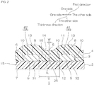
- a wiring circuit board 1 of one embodiment of a wiring circuit board of the present invention is described with reference to FIGS. 1 and 2 .
- the magnetic wiring circuit board 1 has one surface and the other surface in a thickness direction facing each other in the thickness direction, and has a sheet shape extending in a plane direction (direction perpendicular to the thickness direction) (plane direction including a first direction and a second direction to be described later).
- the magnetic wiring circuit board 1 includes an insulating layer 2, a plurality of wirings 3, a magnetic layer 4, and a suppressing portion 5.
- the insulating layer 2 has a sheet shape extending in the plane direction.
- the insulating layer 2 has a first insulating surface 6 that is one surface in the thickness direction and a second insulating surface 7 that is the other surface in the thickness direction.
- the insulating layer 2 is a support material for supporting the plurality of wirings 3 to be described next, and thus, also a support layer for supporting the magnetic wiring circuit board 1.
- the insulating layer 2 has flexibility. Examples of a material of the insulating layer 2 include resin materials such as a polyimide resin, a polyester resin, and an acrylic resin.
- the insulating layer 2 may be a single layer or multiple layers.
- a thickness of the insulating layer 2 is not particularly limited, and is, for example, 1 ⁇ m or more and 1000 ⁇ m or less.
- the plurality of wirings 3 are disposed at intervals from each other in the first direction (the direction corresponding to a right-left direction in FIG. 2 and included in the plane direction) on the first insulating surface 6 of the insulating layer 2.
- the wiring 3 has a first wiring 3A, a second wiring 3B, and a third wiring 3C disposed in parallel at intervals in the first direction.
- the first wiring 3A, the second wiring 3B, and the third wiring 3C are disposed in order from one side toward the other side in the first direction.
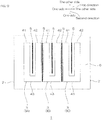
- a shape of each of the plurality of wirings 3 when viewed from the top (viewed in the thickness direction) is, for example, a generally U-shape.
- Each of the plurality of wirings 3 integrally includes a first wiring portion 41 and a second wiring portion 42 as an example of a plurality of wiring portions extending in the second direction perpendicular to the thickness direction and the first direction (the direction corresponding to the depth direction on the plane of the sheet in FIG. 2 ), and a connecting wiring portion 43 for connecting one end portions in the second direction of the first wiring portion 41 and the second wiring portion 42.
- the first wiring portion 41 and the second wiring portion 42 are oppositely disposed at intervals in the first direction (an example of a predetermined direction).
- the first wiring portion 41 and the second wiring portion 42 are adjacent at intervals in a cross-sectional view perpendicular to the second direction (cut surface along the first direction and the thickness direction) (cut surface shown in FIG. 2 ).
- the plurality of first wiring portions 41 and the plurality of second wiring portions 42 are provided in the magnetic wiring circuit board 1, since the plurality of wirings 3 are provided.
- a cross-sectional shape of each of the first wiring portion 41 and the second wiring portion 42 (to be more specific, the cross-sectional shape when cut along the thickness direction and the first direction) is not particularly limited, and may be, for example, a generally rectangular shape.
- Each of the first wiring portion 41 and the second wiring portion 42 integrally includes a first wiring surface 8 which is the one surface in the thickness direction disposed oppositely at intervals on one side in the thickness direction with respect to the first insulating surface 6 of the insulating layer 2, a second wiring surface 9 in contact with the first insulating surface 6 of the insulating layer 2, and third wiring surfaces 10 which are side surfaces for connecting both end edges in the first direction of the first wiring surface 8 and the second wiring surface 9.
- the first wiring surface 8 is a flat surface along the first direction.
- the second wiring surface 9 is a flat surface parallel to the first wiring surface 8.
- the third wiring surfaces 10 extend along the thickness direction.
- the two third wiring surfaces 10 are provided in each of the first wiring portion 41 and the second wiring portion 42.
- the two third wiring surfaces 10 are oppositely disposed at intervals in the first direction.
- the connecting wiring portion 43 has the same cross-sectional shape as each of the first wiring portion 41 and the second wiring portion 42.
- Examples of a material of the wiring 3 include metals (conductors) such as copper.
- the wiring 3 has a thickness of, for example, 10 ⁇ m or more, preferably 30 ⁇ m or more, and for example, 500 ⁇ m or less, preferably 250 ⁇ m or less.
- a width of the first wiring portion 41 and the second wiring portion 42 is, for example, 20 ⁇ m or more and 2000 ⁇ m or less.
- An interval between the first wiring portion 41 and the second wiring portion 42 is, for example, 20 ⁇ m or more, preferably 50 ⁇ m or more, and for example, 2000 ⁇ m or less, preferably 1500 ⁇ m or less.
- a ratio (thickness/width) of the thickness of the wiring 3 (the first wiring portion 41 and the second wiring portion 42) to the width of the first wiring portion 41 and the second wiring portion 42 is, for example, 0.005 or more, preferably 0.015 or more, and for example, 25 or less, preferably 12.5 or less.
- a ratio (thickness/interval) of the thickness of the wiring 3 to the interval between the first wiring portion 41 and the second wiring portion 42 is, for example, 0.005 or more, preferably 0.02 or more, and for example, 25 or less, preferably 5 or less.
- the wiring 3, together with the insulating layer 2 described above, is provided in a wiring circuit board 15.
- the wiring circuit board 15 includes the insulating layer 2 and the plurality of wirings 3.
- the wiring circuit board 15 consists of only the insulating layer 2 and the plurality of wirings 3.
- the magnetic layer 4 has a sheet shape extending in the plane direction.
- the magnetic layer 4 is disposed on the first insulating surface 6 of the insulating layer 2 so as to embed the plurality of wirings 3.
- the magnetic layer 4 has a first magnetic surface 11 and a second magnetic surface 12 disposed at intervals on the other side in the thickness direction of the first magnetic surface 11.
- the first magnetic surface 11 is disposed at intervals on one side in the thickness direction with respect to at least the first wiring surface 8 of the first wiring portion 41 and the second wiring portion 42.
- the first magnetic surface 11 includes a plurality of convex portions 13 which are raised toward one side in the thickness direction corresponding to the first wiring portion 41 and the second wiring portion 42, and a recessed portion 14 which is disposed between the convex portions 13 adjacent to each other and sinks toward the other side in the thickness direction with respect to the convex portion 13.
- the recessed portion 14 (more specifically, the other end edge in the thickness direction of the recessed portion 14) is located at intervals on one side in the thickness direction relative to a phantom line IL connecting the first wiring surfaces 8 of the first wiring portion 41 and the second wiring portion 42.
- the second magnetic surface 12 covers the first insulating surface 6 exposed from the wiring 3 in the insulating layer 2, and the first wiring surface 8 and the third wiring surfaces 10 of the wiring 3.
- An example of a material of the magnetic layer 4 includes a magnetic composition containing magnetic particles and a resin component.
- the magnetic particles include soft magnetic particles such as Sendust from the viewpoint of magnetic properties.
- the resin component include thermosetting resins such as an epoxy resin composition containing an epoxy resin, a curing agent, and a curing accelerator.
- Such a magnetic composition is described in, for example, Japanese Unexamined Patent Publications No. 2017-005115 and 2015-092543 .
- a content ratio of the magnetic particles in the magnetic layer 4 is, for example, 50% by volume or more, preferably 55% by volume or more, and for example, 95% by volume or less, preferably 90% by volume or less.
- the relative permeability of the magnetic layer 4 is, for example, 3 or more, preferably 5 or more, more preferably 10 or more, and for example, 1000 or less.
- the suppressing portion 5 suppresses magnetic coupling of the two wiring portions adjacent to each other.
- the suppressing portion 5 is formed so as to extend from the first magnetic surface 11 of the magnetic layer 4 toward the other side in the thickness direction relative to the phantom line IL connecting the first wiring surfaces 8 of the first wiring portion 41 and the second wiring portion 42 in the magnetic layer 4 between the second wiring portion 42 of one wiring 3 and the first wiring portion 41 of the other wiring 3 adjacent to the one wiring 3 in the two wirings 3 adjacent to each other (the one wiring 3 and the other wiring 3).
- the suppressing portion 5 is formed between the second wiring portion 42 of the first wiring 3A and the first wiring portion 41 of the second wiring 3B, and between the second wiring portion 42 of the second wiring 3B and the first wiring portion 41 of the third wiring 3C.
- the suppressing portion 5 reaches the first insulating surface 6 of the insulating layer 2 from the first magnetic surface 11 of the magnetic layer 4.
- the suppressing portion 5 is a slit (void portion, gap, opening portion) 25 formed in the magnetic layer 4.
- the suppressing portion 5 consists of only the slit 25 (unlike the modified example shown in FIG. 6 to be described later, does not include a filling portion 20).
- the suppressing portion 5 has a generally linear cross-sectional shape extending from the recessed portion 14 of the magnetic layer 4 along the thickness direction.
- the suppressing portion 5 has a shape in which a width (length in the first direction) W thereof is the same in the thickness direction.
- the suppressing portion 5 divides (separates) the magnetic layer 4 in the first direction in a cross-sectional view (cross section along the thickness direction and the first direction).
- the suppressing portion 5 is formed between the two wiring portions so as to be parallel to them that are adjacent to each other along the second direction.
- the suppressing portion 5 has, for example, a generally straight shape when viewed from the top along the second wiring portion 42 of the one wiring 3 and the first wiring portion 41 of the other wiring 3.
- a ratio (W/S) of the width (length in the first direction) W of the suppressing portion 5 to an interval S between the first wiring portion 41 and the second wiring portion 42 adjacent to each other is, for example, 0.7 or less, preferably 0.5 or less, more preferably 0.4 or less, further more preferably 0.3 or less, particularly preferably 0.2 or less, most preferably 0.1 or less, and for example, 0.01 or more.
- the ratio (W/S) described above is the above-described upper limit or less, it is possible to ensure high inductance in the magnetic wiring circuit board 1 by suppressing an excessive decrease in the relative permeability between the wirings 3.
- the length (width) W in the first direction of the suppressing portion 5 is, for example, 100 ⁇ m or less, preferably 80 ⁇ m or less, more preferably 60 ⁇ m or less, and for example, 1 ⁇ m or more.
- a length in the thickness direction of the suppressing portion 5 is the same as the thickness of the magnetic layer 4 in the recessed portion 14.
- the relative permeability in the suppressing portion 5 is substantially 1 (in detail, a value approximating 1 of the relative permeability of the vacuum), when the suppressing portion 5 is the slit 25 and the air is present in the suppressing portion 5.
- a thickness of the magnetic wiring circuit board 1, as its maximum thickness, is, for example, 30 ⁇ m or more, preferably 50 ⁇ m or more, and for example, 1000 ⁇ m or less, preferably 800 ⁇ m or less.
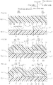
- the wiring circuit board 15 including the insulating layer 2 and the wiring 3 is prepared.
- a magnetic sheet 16 is prepared.
- the above-described magnetic composition containing the magnetic particles and the resin component preferably, a B-stage thermosetting resin
- the resin component preferably, a B-stage thermosetting resin
- the magnetic sheet 16 embeds the plurality of wirings 3 in the wiring circuit board 15.
- the magnetic sheet 16 contains the B-stage thermosetting resin, the magnetic sheet 16 is thermally pressed toward the wiring circuit board 15.
- the magnetic sheet 16 is formed (molded) into a shape corresponding to the wiring 3 (at least the first wiring portion 41 and the second wiring portion 42). That is, the magnetic layer 4 is formed from the magnetic sheet 16.
- the suppressing portion 5 is not yet formed in the magnetic layer 4.
- the suppressing portion 5 is formed in the magnetic layer 4.
- a cutting device (cutter) is used.
- Examples of the cutting device include a contact-type cutting device that is in physical contact with the magnetic layer 4 such as a dicing device and a non-contact-type cutting device that is not in physical contact with the magnetic layer 4 such as a laser device.
- a contact-type cutting device is used, from the viewpoint of shortening the working time (tact time), preferably, a non-contact-type cutting device is used.
- a dicing device as an example of a contact-type cutting device includes a support base (not shown), a dicing saw 17 which is oppositely disposed at a distance therefrom, and a moving device for moving the dicing saw 17 (not shown).
- An example of the dicing saw 17 includes a dicing blade having a disk shape.
- the wiring circuit board 15 and the magnetic layer 4 are installed on the support base (not shown) of the dicing device.
- the dicing saw 17 is disposed at intervals on one side in the thickness direction of the magnetic layer 4. Subsequently, the peripheral end of the dicing saw 17 is brought into contact with the first magnetic surface 11 (specifically, the recessed portion 14) of the magnetic layer 4.
- the dicing saw 17 is moved (pulled down) toward the other side in the thickness direction until its peripheral end reaches the first insulating surface 6 of the insulating layer 2. Thereafter, the dicing saw 17 is moved along the second direction.
- the suppressing portion 5 that is the slit 25 is formed along the second direction.
- the magnetic wiring circuit board 1 including the wiring circuit board 15, the magnetic layer 4, and the suppressing portion 5 is obtained.
- the magnetic layer 4 contains the B-stage thermosetting resin, if necessary, the magnetic layer 4 is brought into a C-stage state (fully cured), for example, by heating.
- the magnetic wiring circuit board 1 is, for example, used in wireless power transmission (wireless power supply and/or wireless power receiving), wireless communication, sensors, passive components, and the like.
- the suppressing portion 5 extends from the first magnetic surface 11 of the magnetic layer 4 toward the other side in the thickness direction relative to the phantom line IL connecting the first wiring surfaces 8 of the two wirings 3 adjacent to each other (the second wiring portion 42 of the one wiring 3, and the first wiring portion 41 of the other wiring 3). Therefore, it is possible to suppress the magnetic coupling of the two wirings 3. Therefore, it is possible to suppress the occurrence of noise in the two wirings 3.
- the suppressing portion 5 reaches the first insulating surface 6 of the insulating layer 2. Therefore, by more reliably suppressing the magnetic coupling of the two wirings 3, it is possible to more reliably suppress the occurrence of noise in the two wirings 3 (the second wiring portion 42 of the one wiring 3, and the first wiring portion 41 of the other wiring 3).
- the suppressing portion 5 is the slit 25, it is possible to suppress the occurrence of noise in the two wirings 3 (the second wiring portion 42 of the one wiring 3, and the first wiring portion 41 of the other wiring 3) in a simple structure.
- the ratio of the width W of the suppressing portion 5 to the interval S between the plurality of wirings 3 is as low as 0.4 or less, it is possible to ensure high inductance by suppressing an excessive decrease in the relative permeability between the wirings 3.
- the suppressing portion 5 extends from the first magnetic surface 11 of the magnetic layer 4 to reach the first insulating surface 6 of the insulating layer 2.
- the suppressing portion 5 does not reach the first insulating surface 6 of the insulating layer 2, and is separated from the first insulating surface 6.
- the suppressing portion 5 is a suppression recessed portion that is recessed from the first magnetic surface 11.
- the suppressing portion 5 is opened toward one side in the thickness direction.
- the suppressing portion 5 has a bottom portion 18 located on the other side in the thickness direction relative to the above-described phantom line IL.
- the bottom portion 18 is located between the phantom line IL and the first insulating surface 6 of the insulating layer 2.
- a depth of the suppressing portion 5 is not particularly limited as long as the bottom portion 18 is located on the other side in the thickness direction relative to the phantom line IL.
- a ratio of a distance L between the bottom portion 18 and the phantom line IL to the thickness of the wiring 3 is, for example, 0.1 or more, preferably 0.2 or more, and for example, below 1, preferably 0.9 or less.
- the ratio is the above-described lower limit or more, the magnetic coupling of the wirings 3 adjacent to each other can be effectively suppressed.
- the ratio is the above-described upper limit or less, the strength of the magnetic layer 4 can be ensured.
- the magnetic layer 4 is in contact with the first wiring surface 8 and the third wiring surfaces 10 of the wiring 3. That is, the magnetic layer 4 is directly disposed on the first wiring surface 8 and the third wiring surfaces 10.
- the magnetic layer 4 may not be in contact with the first wiring surface 8 and the third wiring surfaces 10 of the wiring 3, and may be disposed indirectly in the first wiring surface 8 and the third wiring surface 10.
- a second insulating layer 19 is interposed between the magnetic layer 4 and the wiring 3.
- the second insulating layer 19 has a thin film shape along the first wiring surface 8 and the third wiring surfaces 10 of the wiring 3.
- the second insulating layer 19 does not have, for example, magnetic properties.
- examples of a material of the second insulating layer 19 include resin materials without containing the magnetic particles.
- the resin material of the second insulating layer 19 is the same as the resin material illustrated in the insulating layer 2.
- the second insulating layer 19 has a thickness of, for example, 10 ⁇ m or less and 0.1 ⁇ m or more.
- the suppressing portion 5 consists of only the slit 25.
- the suppressing portion 5 can also include the slit 25 and the filling portion 20 that fills the slit 25.
- the suppressing portion 5 preferably consists of only the slit 25 and the filling portion 20.
- Examples of a material of the filling portion 20 include low-permeability materials.
- Examples of the low-permeability material include resin materials without containing the magnetic particles.
- the suppressing portion 5 consists of only the slit 25.
- the relative permeability of the suppressing portion 5 can be reliably set lower than that of the suppressing portion 5 further including the filling portion 20 shown in FIG. 6 , so that the magnetic coupling of the wirings 3 can be effectively suppressed.
- the insulating layer 2 may be also a magnetic insulating layer containing the magnetic particles and having the magnetic properties.
- the magnetic layer 4 is formed of the magnetic sheet 16.
- a varnish of a magnetic composition may be also prepared and applied to form the magnetic layer 4.
- the magnetic layer 4 and the suppressing portion 5 are formed by separate steps. Alternatively, though not shown, it is also possible to form them in one step. For example, a wall member (or post) having the same shape as the suppressing portion 5 is installed on the first insulating surface 6 between the two wirings 3, subsequently, the magnetic layer 4 is formed into a shape corresponding to the wall member, and then, the wall member is removed (e.g., pulled toward one side in the thickness direction). As a result, the magnetic layer 4 and the suppressing portion 5 are formed at one time.
- the suppressing portion 5 has a generally linear cross-sectional shape extending from the first magnetic surface 11 of the magnetic layer 4 along the thickness direction.
- the cross-sectional shape of the suppressing portion 5 is not limited thereto.
- the suppressing portion 5 may also have the opening area (or the opposing length in the first direction) in a tapered shape that becomes gradually smaller (narrower) toward the other side in the thickness direction.
- the width W of the suppressing portion 5 is defined as the length on the phantom line IL in the suppressing portion 5.
- the width W of the suppressing portion 5 is adjusted so that the W/S satisfies, for example, 0.4 or less, the same function and effect as described above (suppression of an excessive decrease in the relative permeability between the wirings 3) can be achieved.
- the suppressing portion 5 is formed between the two wirings 3 adjacent to each other.
- the suppressing portion 5 may be also disposed between the two wiring portions in the one wiring 3, i.e., between the first wiring portion 41 and the second wiring portion 42.
- the suppressing portion 5 may be also disposed both between the two wirings 3 adjacent to each other, and between the first wiring portion 41 and the second wiring portion 42 in the one wiring 3.
- the suppressing portion 5 can also have a wide portion which is wider than the width W defined above and disposed on the other side in the thickness direction relative to the phantom line IL.
- a shape of the wide portion is not particularly limited, and includes, for example, a generally circular arc shape, a generally wave shape, and the like.
- a width (the second width, the length in the first direction) of the wide portion is, for example, 1.4 or less and above 1 with respect to the width (the first width) W described above.
- the magnetic layer 4 is brought into a C-stage state after forming the suppressing portion 5, and the order may be reversed.
- a pattern shape of the wiring 3 is not particularly limited, and includes, for example, a generally coil shape, a generally loop shape, a generally S shape, and the like. Examples
- the wiring circuit board 15 including the insulating layer 2 and the plurality of wirings 3 was prepared.
- the insulating layer 2 was made of a polyimide resin and had a thickness of 5 ⁇ m.
- the plurality of wirings 3 were made of copper and had a thickness of 100 ⁇ m.
- Each of the plurality of wirings 3 (the first wiring 3A, the second wiring 3B, and the third wiring 3C) had the first wiring portion 41, the second wiring portion 42, and the connecting wiring portion 43.
- the first wiring portion 41 and the second wiring portion 42 had a width of 300 ⁇ m and an interval of 300 ⁇ m.
- the interval S between the second wiring portion 42 of the one wiring 3 and the first wiring portion 41 of the other wiring 3 was 100 ⁇ m.
- the magnetic sheet 16 was prepared separately.
- the magnetic sheet 16 was formed from a magnetic composition containing 60% by volume of Sendust and 40% by volume of a thermosetting resin (epoxy resin composition).
- the magnetic sheet 16 was thermally pressed toward the wiring circuit board 15 to form the magnetic layer 4.
- the slit 25 extending from the first magnetic surface 11 of the magnetic layer 4 to reach the first insulating surface 6 of the insulating layer 2 was formed in the magnetic layer 4 with the dicing saw 17, thereby forming the suppressing portion 5.
- the width W of the suppressing portion 5 was 40 ⁇ m.
- the ratio (W/S) of the interval S between the plurality of wirings 3 to the width W of the suppressing portion 5 was 0.4.
- the magnetic wiring circuit board 1 was obtained in the same manner as in Example 1, except that the shape, the size, and the like of the suppressing portion 5 were changed according to Table 1.
- the magnetic wiring circuit board 1 prior to forming the suppressing portion 5 (in the middle of manufacturing) shown in FIG. 3B was obtained as the magnetic wiring circuit board 1 of Comparative Example 1 as it was.
- the magnetic wiring circuit board 1 was not provided with the suppressing portion 5.
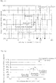
- One end portions in the second direction of the first wiring portion 41 and the second wiring portion 42 in the second wiring 3B in each of the magnetic wiring circuit boards 1 of Examples 1 and 2, and Comparative Example 1 were connected to an impedance analyzer (manufactured by Agilent Technologies, Inc.: 4294A) to measure the inductance of the other wiring 3 adjacent to the first wiring 3, and this inductance was used as the reference inductance.
- an impedance analyzer manufactured by Agilent Technologies, Inc.: 4294A
- the inductance of the second wiring 3 (3B) was measured in a state where the one end portions in the second direction of the first wiring portion 41 and the second wiring portion 42 of the first wiring 3A were connected to each other with another wiring to short-circuit the first wiring 3A, and the difference between this value and the reference inductance described above was obtained. By dividing this by the reference inductance, the first rate of change of the inductance was obtained.
- the inductance of the second wiring 3B was measured in a state where the one end portions in the second direction of the first wiring portion 41 and the second wiring portion 42 of the third wiring 3 (3C) were connected to each other with another wiring to short-circuit the third wiring 3C (i.e., a state where both the first wiring 3A and the third wiring 3C located on both sides in the first direction of the second wiring 3B were short-circuited), and the difference between this value and the reference inductance described above was obtained. By dividing this by the reference inductance, the second rate of change of the inductance was obtained.
- the occupation area of the second wiring 3B and the magnetic layer 4 adjacent thereto on one side in first direction thereof in the magnetic wiring circuit board 1 of Examples 1 and 2, and Comparative Example 1 i.e., the occupation area of the inductor by the second wiring 3B and the corresponding magnetic layer 4
- Comparative Example 1 the occupation area of the inductor by the second wiring 3B and the corresponding magnetic layer 4
- the inductance density was obtained.
- Example 1 a single mark (in Example 1, ⁇ (circle)) was a plot of the first rate of change of the inductance and the corresponding inductance density.
- a double mark in Example 1, ⁇ (double rings) was a plot of the second rate of change of the inductance and the corresponding inductance density.
- Medium black in Example 1, ⁇ (black circle) was a plot of the rate of change of the reference inductance (i.e., zero) and the corresponding inductance density.
- Example 1 When Examples 1 and 2 are compared, it can be seen that the influence of the magnetic coupling of the wirings 3 is smaller in Example 1 in which the suppressing portion 5 reaches the first insulating surface 6 than in Example 2 in which the suppressing portion 5 reaches halfway in the thickness direction of the insulating layer 2.
- the magnetic wiring circuit board of the present invention is, for example, used in wireless power transmission (wireless power supply and/or wireless power receiving), wireless communication, sensors, passive components, and the like.
Landscapes
- Engineering & Computer Science (AREA)
- Power Engineering (AREA)
- Microelectronics & Electronic Packaging (AREA)
- Physics & Mathematics (AREA)
- Electromagnetism (AREA)
- Manufacturing & Machinery (AREA)
- Structure Of Printed Boards (AREA)
- Shielding Devices Or Components To Electric Or Magnetic Fields (AREA)
- Coils Or Transformers For Communication (AREA)
- Parts Printed On Printed Circuit Boards (AREA)
- Laminated Bodies (AREA)
- Insulated Metal Substrates For Printed Circuits (AREA)
- Soft Magnetic Materials (AREA)
Applications Claiming Priority (2)
| Application Number | Priority Date | Filing Date | Title |
|---|---|---|---|
| JP2018074801A JP7220948B2 (ja) | 2018-04-09 | 2018-04-09 | 磁性配線回路基板 |
| PCT/JP2019/014644 WO2019198569A1 (ja) | 2018-04-09 | 2019-04-02 | 磁性配線回路基板 |
Publications (2)
| Publication Number | Publication Date |
|---|---|
| EP3780032A1 true EP3780032A1 (de) | 2021-02-17 |
| EP3780032A4 EP3780032A4 (de) | 2021-12-29 |
Family
ID=68163577
Family Applications (1)
| Application Number | Title | Priority Date | Filing Date |
|---|---|---|---|
| EP19784782.5A Pending EP3780032A4 (de) | 2018-04-09 | 2019-04-02 | Magnetische leiterplatte |
Country Status (7)
| Country | Link |
|---|---|
| US (1) | US11006515B2 (de) |
| EP (1) | EP3780032A4 (de) |
| JP (1) | JP7220948B2 (de) |
| KR (1) | KR102655610B1 (de) |
| CN (1) | CN111919269B (de) |
| TW (1) | TWI784156B (de) |
| WO (1) | WO2019198569A1 (de) |
Families Citing this family (4)
| Publication number | Priority date | Publication date | Assignee | Title |
|---|---|---|---|---|
| JP7565721B2 (ja) * | 2020-07-27 | 2024-10-11 | 日東電工株式会社 | インダクタの製造方法 |
| JP7546397B2 (ja) | 2020-07-27 | 2024-09-06 | 日東電工株式会社 | インダクタ |
| WO2022092791A1 (ko) | 2020-10-27 | 2022-05-05 | 주식회사 엘지화학 | 이물제거장치 |
| JP7685571B2 (ja) * | 2023-09-29 | 2025-05-29 | 株式会社ダイヘン | トランス用のコイル基板 |
Family Cites Families (25)
| Publication number | Priority date | Publication date | Assignee | Title |
|---|---|---|---|---|
| JPS5981022U (ja) * | 1982-11-24 | 1984-05-31 | ティーディーケイ株式会社 | 積層複合部品 |
| DE3776359D1 (en) * | 1986-02-13 | 1992-03-12 | Sony Corp | Duennschichtmagnetkopf. |
| JP3220981B2 (ja) | 1989-11-17 | 2001-10-22 | ティーディーケイ株式会社 | 混成集積回路部品の構造 |
| JPH05152130A (ja) * | 1991-11-26 | 1993-06-18 | Matsushita Electric Ind Co Ltd | 複合インダクタおよびその製造方法 |
| JP3200954B2 (ja) * | 1992-05-01 | 2001-08-20 | 株式会社村田製作所 | 複合電子部品 |
| JP3233306B2 (ja) * | 1993-04-12 | 2001-11-26 | ティーディーケイ株式会社 | 積層型ノイズ吸収素子複合体 |
| JPH10270256A (ja) * | 1997-03-21 | 1998-10-09 | Taiyo Yuden Co Ltd | 電子部品 |
| KR20030043747A (ko) * | 2001-11-28 | 2003-06-02 | 후지 샤신 필름 가부시기가이샤 | 자기전사용 마스터 담체 및 자기전사방법 |
| JP2004079090A (ja) * | 2002-08-20 | 2004-03-11 | Hitachi Ltd | 記録再生分離型磁気ヘッド |
| JP2004363291A (ja) | 2003-06-04 | 2004-12-24 | Murata Mfg Co Ltd | 積層型電子部品およびその製造方法 |
| JP4547889B2 (ja) * | 2003-10-21 | 2010-09-22 | Tdk株式会社 | 磁気結合素子 |
| JP2005333081A (ja) | 2004-05-21 | 2005-12-02 | Shinko Electric Ind Co Ltd | 基板、半導体装置及び基板の製造方法 |
| JP2006031756A (ja) * | 2004-07-12 | 2006-02-02 | Tdk Corp | 磁気記録媒体 |
| US6996892B1 (en) * | 2005-03-24 | 2006-02-14 | Rf Micro Devices, Inc. | Circuit board embedded inductor |
| CN100593362C (zh) * | 2005-07-04 | 2010-03-03 | 欧姆龙株式会社 | 电路基板、电子设备和电源装置 |
| TWI319581B (en) | 2006-08-08 | 2010-01-11 | Murata Manufacturing Co | Laminated coil component and method for manufacturing the same |
| KR100829569B1 (ko) * | 2006-10-18 | 2008-05-14 | 삼성전자주식회사 | 자구벽 이동을 이용한 반도체 장치 및 그의 제조방법 |
| JP2010028695A (ja) * | 2008-07-24 | 2010-02-04 | Murata Mfg Co Ltd | ノイズフィルタ部品及びコイル部品 |
| JP5134580B2 (ja) * | 2009-05-01 | 2013-01-30 | 日東電工株式会社 | 配線回路基板およびそれを備えた磁気ヘッド駆動装置 |
| CN103377795B (zh) * | 2012-04-24 | 2016-01-27 | 乾坤科技股份有限公司 | 电磁器件及其制作方法 |
| JP6377336B2 (ja) * | 2013-03-06 | 2018-08-22 | 株式会社東芝 | インダクタ及びその製造方法 |
| JP6125328B2 (ja) | 2013-05-27 | 2017-05-10 | 日東電工株式会社 | 軟磁性フィルム積層回路基板の製造方法 |
| JP6567259B2 (ja) | 2013-10-01 | 2019-08-28 | 日東電工株式会社 | 軟磁性樹脂組成物、軟磁性フィルム、軟磁性フィルム積層回路基板および位置検出装置 |
| KR102105396B1 (ko) | 2015-01-28 | 2020-04-28 | 삼성전기주식회사 | 칩 전자부품 및 칩 전자부품의 실장 기판 |
| JP2017005115A (ja) | 2015-06-10 | 2017-01-05 | 日東電工株式会社 | コイルモジュールおよびその製造方法 |
-
2018
- 2018-04-09 JP JP2018074801A patent/JP7220948B2/ja active Active
-
2019
- 2019-04-02 KR KR1020207028405A patent/KR102655610B1/ko active Active
- 2019-04-02 US US17/044,448 patent/US11006515B2/en active Active
- 2019-04-02 CN CN201980022592.8A patent/CN111919269B/zh active Active
- 2019-04-02 WO PCT/JP2019/014644 patent/WO2019198569A1/ja not_active Ceased
- 2019-04-02 EP EP19784782.5A patent/EP3780032A4/de active Pending
- 2019-04-08 TW TW108112099A patent/TWI784156B/zh active
Also Published As
| Publication number | Publication date |
|---|---|
| CN111919269B (zh) | 2023-02-17 |
| WO2019198569A1 (ja) | 2019-10-17 |
| KR102655610B1 (ko) | 2024-04-08 |
| TW201944436A (zh) | 2019-11-16 |
| US11006515B2 (en) | 2021-05-11 |
| US20210037640A1 (en) | 2021-02-04 |
| TWI784156B (zh) | 2022-11-21 |
| EP3780032A4 (de) | 2021-12-29 |
| JP7220948B2 (ja) | 2023-02-13 |
| KR20200140268A (ko) | 2020-12-15 |
| CN111919269A (zh) | 2020-11-10 |
| JP2019186365A (ja) | 2019-10-24 |
Similar Documents
| Publication | Publication Date | Title |
|---|---|---|
| US11006515B2 (en) | Magnetic wiring circuit board | |
| US9030287B2 (en) | Common mode noise filter | |
| US9362042B2 (en) | Electronic component | |
| KR101474166B1 (ko) | 칩 전자부품 및 그 제조방법 | |
| KR102214223B1 (ko) | 코일 부품 | |
| US20150028988A1 (en) | Laminated coil | |
| US9966183B2 (en) | Multilayer coil | |
| JP6760500B2 (ja) | コイル部品 | |
| KR20130063363A (ko) | 커먼 모드 노이즈 필터 | |
| US11742126B2 (en) | Inductor | |
| KR20160076656A (ko) | 파워인덕터 및 그 제조방법 | |
| US20090151985A1 (en) | Method of dicing a circuit board sheet and package circuit board | |
| US20260128207A1 (en) | Inductor array | |
| CN112542287A (zh) | 电感器、电路板和电子设备 | |
| KR20160018615A (ko) | 코일 부품 및 이의 제조 방법 | |
| US20190295764A1 (en) | Coil component and electronic device | |
| US12198843B2 (en) | Inductor | |
| KR102893911B1 (ko) | 인덕터 | |
| JP2024063233A (ja) | コイル部品及びコイル部品の製造方法 | |
| JP7747430B2 (ja) | インダクタ | |
| KR101046879B1 (ko) | 초박형 파워 인덕터 | |
| EP1414280A2 (de) | Vielschichtelektronikbauteil und sein Herstellungsverfahren | |
| US20200343032A1 (en) | Coil component | |
| CN113470925A (zh) | 线圈部件 | |
| JP2001110641A (ja) | 積層インピーダンス素子 |
Legal Events
| Date | Code | Title | Description |
|---|---|---|---|
| STAA | Information on the status of an ep patent application or granted ep patent |
Free format text: STATUS: THE INTERNATIONAL PUBLICATION HAS BEEN MADE |
|
| PUAI | Public reference made under article 153(3) epc to a published international application that has entered the european phase |
Free format text: ORIGINAL CODE: 0009012 |
|
| STAA | Information on the status of an ep patent application or granted ep patent |
Free format text: STATUS: REQUEST FOR EXAMINATION WAS MADE |
|
| 17P | Request for examination filed |
Effective date: 20201005 |
|
| AK | Designated contracting states |
Kind code of ref document: A1 Designated state(s): AL AT BE BG CH CY CZ DE DK EE ES FI FR GB GR HR HU IE IS IT LI LT LU LV MC MK MT NL NO PL PT RO RS SE SI SK SM TR |
|
| AX | Request for extension of the european patent |
Extension state: BA ME |
|
| DAV | Request for validation of the european patent (deleted) | ||
| DAX | Request for extension of the european patent (deleted) | ||
| REG | Reference to a national code |
Ref country code: DE Ref legal event code: R079 Free format text: PREVIOUS MAIN CLASS: H01F0017000000 Ipc: H05K0001160000 |
|
| A4 | Supplementary search report drawn up and despatched |
Effective date: 20211126 |
|
| RIC1 | Information provided on ipc code assigned before grant |
Ipc: H05K 3/28 20060101ALN20211122BHEP Ipc: H01F 41/04 20060101ALI20211122BHEP Ipc: H01F 5/00 20060101ALI20211122BHEP Ipc: H05K 1/16 20060101AFI20211122BHEP |
|
| STAA | Information on the status of an ep patent application or granted ep patent |
Free format text: STATUS: EXAMINATION IS IN PROGRESS |
|
| 17Q | First examination report despatched |
Effective date: 20240920 |