EP3792736A1 - Afficheur et son procédé de fabrication - Google Patents
Afficheur et son procédé de fabrication Download PDFInfo
- Publication number
- EP3792736A1 EP3792736A1 EP20206343.4A EP20206343A EP3792736A1 EP 3792736 A1 EP3792736 A1 EP 3792736A1 EP 20206343 A EP20206343 A EP 20206343A EP 3792736 A1 EP3792736 A1 EP 3792736A1
- Authority
- EP
- European Patent Office
- Prior art keywords
- layer
- touch
- display area
- fan
- electrode
- Prior art date
- Legal status (The legal status is an assumption and is not a legal conclusion. Google has not performed a legal analysis and makes no representation as to the accuracy of the status listed.)
- Granted
Links
Images













Classifications
-
- G—PHYSICS
- G06—COMPUTING OR CALCULATING; COUNTING
- G06F—ELECTRIC DIGITAL DATA PROCESSING
- G06F3/00—Input arrangements for transferring data to be processed into a form capable of being handled by the computer; Output arrangements for transferring data from processing unit to output unit, e.g. interface arrangements
- G06F3/01—Input arrangements or combined input and output arrangements for interaction between user and computer
- G06F3/03—Arrangements for converting the position or the displacement of a member into a coded form
- G06F3/041—Digitisers, e.g. for touch screens or touch pads, characterised by the transducing means
- G06F3/0412—Digitisers structurally integrated in a display
-
- G—PHYSICS
- G02—OPTICS
- G02F—OPTICAL DEVICES OR ARRANGEMENTS FOR THE CONTROL OF LIGHT BY MODIFICATION OF THE OPTICAL PROPERTIES OF THE MEDIA OF THE ELEMENTS INVOLVED THEREIN; NON-LINEAR OPTICS; FREQUENCY-CHANGING OF LIGHT; OPTICAL LOGIC ELEMENTS; OPTICAL ANALOGUE/DIGITAL CONVERTERS
- G02F1/00—Devices or arrangements for the control of the intensity, colour, phase, polarisation or direction of light arriving from an independent light source, e.g. switching, gating or modulating; Non-linear optics
- G02F1/01—Devices or arrangements for the control of the intensity, colour, phase, polarisation or direction of light arriving from an independent light source, e.g. switching, gating or modulating; Non-linear optics for the control of the intensity, phase, polarisation or colour
- G02F1/13—Devices or arrangements for the control of the intensity, colour, phase, polarisation or direction of light arriving from an independent light source, e.g. switching, gating or modulating; Non-linear optics for the control of the intensity, phase, polarisation or colour based on liquid crystals, e.g. single liquid crystal display cells
- G02F1/133—Constructional arrangements; Operation of liquid crystal cells; Circuit arrangements
- G02F1/136—Liquid crystal cells structurally associated with a semi-conducting layer or substrate, e.g. cells forming part of an integrated circuit
- G02F1/1362—Active matrix addressed cells
-
- G—PHYSICS
- G02—OPTICS
- G02F—OPTICAL DEVICES OR ARRANGEMENTS FOR THE CONTROL OF LIGHT BY MODIFICATION OF THE OPTICAL PROPERTIES OF THE MEDIA OF THE ELEMENTS INVOLVED THEREIN; NON-LINEAR OPTICS; FREQUENCY-CHANGING OF LIGHT; OPTICAL LOGIC ELEMENTS; OPTICAL ANALOGUE/DIGITAL CONVERTERS
- G02F1/00—Devices or arrangements for the control of the intensity, colour, phase, polarisation or direction of light arriving from an independent light source, e.g. switching, gating or modulating; Non-linear optics
- G02F1/01—Devices or arrangements for the control of the intensity, colour, phase, polarisation or direction of light arriving from an independent light source, e.g. switching, gating or modulating; Non-linear optics for the control of the intensity, phase, polarisation or colour
- G02F1/13—Devices or arrangements for the control of the intensity, colour, phase, polarisation or direction of light arriving from an independent light source, e.g. switching, gating or modulating; Non-linear optics for the control of the intensity, phase, polarisation or colour based on liquid crystals, e.g. single liquid crystal display cells
- G02F1/133—Constructional arrangements; Operation of liquid crystal cells; Circuit arrangements
- G02F1/1333—Constructional arrangements; Manufacturing methods
- G02F1/1345—Conductors connecting electrodes to cell terminals
-
- G—PHYSICS
- G02—OPTICS
- G02F—OPTICAL DEVICES OR ARRANGEMENTS FOR THE CONTROL OF LIGHT BY MODIFICATION OF THE OPTICAL PROPERTIES OF THE MEDIA OF THE ELEMENTS INVOLVED THEREIN; NON-LINEAR OPTICS; FREQUENCY-CHANGING OF LIGHT; OPTICAL LOGIC ELEMENTS; OPTICAL ANALOGUE/DIGITAL CONVERTERS
- G02F1/00—Devices or arrangements for the control of the intensity, colour, phase, polarisation or direction of light arriving from an independent light source, e.g. switching, gating or modulating; Non-linear optics
- G02F1/01—Devices or arrangements for the control of the intensity, colour, phase, polarisation or direction of light arriving from an independent light source, e.g. switching, gating or modulating; Non-linear optics for the control of the intensity, phase, polarisation or colour
- G02F1/13—Devices or arrangements for the control of the intensity, colour, phase, polarisation or direction of light arriving from an independent light source, e.g. switching, gating or modulating; Non-linear optics for the control of the intensity, phase, polarisation or colour based on liquid crystals, e.g. single liquid crystal display cells
- G02F1/133—Constructional arrangements; Operation of liquid crystal cells; Circuit arrangements
- G02F1/1333—Constructional arrangements; Manufacturing methods
- G02F1/133305—Flexible substrates, e.g. plastics, organic film
-
- G—PHYSICS
- G02—OPTICS
- G02F—OPTICAL DEVICES OR ARRANGEMENTS FOR THE CONTROL OF LIGHT BY MODIFICATION OF THE OPTICAL PROPERTIES OF THE MEDIA OF THE ELEMENTS INVOLVED THEREIN; NON-LINEAR OPTICS; FREQUENCY-CHANGING OF LIGHT; OPTICAL LOGIC ELEMENTS; OPTICAL ANALOGUE/DIGITAL CONVERTERS
- G02F1/00—Devices or arrangements for the control of the intensity, colour, phase, polarisation or direction of light arriving from an independent light source, e.g. switching, gating or modulating; Non-linear optics
- G02F1/01—Devices or arrangements for the control of the intensity, colour, phase, polarisation or direction of light arriving from an independent light source, e.g. switching, gating or modulating; Non-linear optics for the control of the intensity, phase, polarisation or colour
- G02F1/13—Devices or arrangements for the control of the intensity, colour, phase, polarisation or direction of light arriving from an independent light source, e.g. switching, gating or modulating; Non-linear optics for the control of the intensity, phase, polarisation or colour based on liquid crystals, e.g. single liquid crystal display cells
- G02F1/133—Constructional arrangements; Operation of liquid crystal cells; Circuit arrangements
- G02F1/1333—Constructional arrangements; Manufacturing methods
- G02F1/1343—Electrodes
-
- G—PHYSICS
- G02—OPTICS
- G02F—OPTICAL DEVICES OR ARRANGEMENTS FOR THE CONTROL OF LIGHT BY MODIFICATION OF THE OPTICAL PROPERTIES OF THE MEDIA OF THE ELEMENTS INVOLVED THEREIN; NON-LINEAR OPTICS; FREQUENCY-CHANGING OF LIGHT; OPTICAL LOGIC ELEMENTS; OPTICAL ANALOGUE/DIGITAL CONVERTERS
- G02F1/00—Devices or arrangements for the control of the intensity, colour, phase, polarisation or direction of light arriving from an independent light source, e.g. switching, gating or modulating; Non-linear optics
- G02F1/01—Devices or arrangements for the control of the intensity, colour, phase, polarisation or direction of light arriving from an independent light source, e.g. switching, gating or modulating; Non-linear optics for the control of the intensity, phase, polarisation or colour
- G02F1/13—Devices or arrangements for the control of the intensity, colour, phase, polarisation or direction of light arriving from an independent light source, e.g. switching, gating or modulating; Non-linear optics for the control of the intensity, phase, polarisation or colour based on liquid crystals, e.g. single liquid crystal display cells
- G02F1/133—Constructional arrangements; Operation of liquid crystal cells; Circuit arrangements
- G02F1/136—Liquid crystal cells structurally associated with a semi-conducting layer or substrate, e.g. cells forming part of an integrated circuit
- G02F1/1362—Active matrix addressed cells
- G02F1/136286—Wiring, e.g. gate line, drain line
-
- G—PHYSICS
- G06—COMPUTING OR CALCULATING; COUNTING
- G06F—ELECTRIC DIGITAL DATA PROCESSING
- G06F3/00—Input arrangements for transferring data to be processed into a form capable of being handled by the computer; Output arrangements for transferring data from processing unit to output unit, e.g. interface arrangements
- G06F3/01—Input arrangements or combined input and output arrangements for interaction between user and computer
- G06F3/03—Arrangements for converting the position or the displacement of a member into a coded form
- G06F3/041—Digitisers, e.g. for touch screens or touch pads, characterised by the transducing means
- G06F3/0416—Control or interface arrangements specially adapted for digitisers
- G06F3/04164—Connections between sensors and controllers, e.g. routing lines between electrodes and connection pads
-
- H—ELECTRICITY
- H10—SEMICONDUCTOR DEVICES; ELECTRIC SOLID-STATE DEVICES NOT OTHERWISE PROVIDED FOR
- H10D—INORGANIC ELECTRIC SEMICONDUCTOR DEVICES
- H10D86/00—Integrated devices formed in or on insulating or conducting substrates, e.g. formed in silicon-on-insulator [SOI] substrates or on stainless steel or glass substrates
- H10D86/40—Integrated devices formed in or on insulating or conducting substrates, e.g. formed in silicon-on-insulator [SOI] substrates or on stainless steel or glass substrates characterised by multiple TFTs
- H10D86/411—Integrated devices formed in or on insulating or conducting substrates, e.g. formed in silicon-on-insulator [SOI] substrates or on stainless steel or glass substrates characterised by multiple TFTs characterised by materials, geometry or structure of the substrates
-
- H—ELECTRICITY
- H10—SEMICONDUCTOR DEVICES; ELECTRIC SOLID-STATE DEVICES NOT OTHERWISE PROVIDED FOR
- H10D—INORGANIC ELECTRIC SEMICONDUCTOR DEVICES
- H10D86/00—Integrated devices formed in or on insulating or conducting substrates, e.g. formed in silicon-on-insulator [SOI] substrates or on stainless steel or glass substrates
- H10D86/40—Integrated devices formed in or on insulating or conducting substrates, e.g. formed in silicon-on-insulator [SOI] substrates or on stainless steel or glass substrates characterised by multiple TFTs
- H10D86/60—Integrated devices formed in or on insulating or conducting substrates, e.g. formed in silicon-on-insulator [SOI] substrates or on stainless steel or glass substrates characterised by multiple TFTs wherein the TFTs are in active matrices
-
- H—ELECTRICITY
- H10—SEMICONDUCTOR DEVICES; ELECTRIC SOLID-STATE DEVICES NOT OTHERWISE PROVIDED FOR
- H10K—ORGANIC ELECTRIC SOLID-STATE DEVICES
- H10K50/00—Organic light-emitting devices
- H10K50/80—Constructional details
- H10K50/84—Passivation; Containers; Encapsulations
- H10K50/844—Encapsulations
-
- H—ELECTRICITY
- H10—SEMICONDUCTOR DEVICES; ELECTRIC SOLID-STATE DEVICES NOT OTHERWISE PROVIDED FOR
- H10K—ORGANIC ELECTRIC SOLID-STATE DEVICES
- H10K59/00—Integrated devices, or assemblies of multiple devices, comprising at least one organic light-emitting element covered by group H10K50/00
- H10K59/10—OLED displays
- H10K59/12—Active-matrix OLED [AMOLED] displays
- H10K59/121—Active-matrix OLED [AMOLED] displays characterised by the geometry or disposition of pixel elements
- H10K59/1213—Active-matrix OLED [AMOLED] displays characterised by the geometry or disposition of pixel elements the pixel elements being TFTs
-
- H—ELECTRICITY
- H10—SEMICONDUCTOR DEVICES; ELECTRIC SOLID-STATE DEVICES NOT OTHERWISE PROVIDED FOR
- H10K—ORGANIC ELECTRIC SOLID-STATE DEVICES
- H10K59/00—Integrated devices, or assemblies of multiple devices, comprising at least one organic light-emitting element covered by group H10K50/00
- H10K59/10—OLED displays
- H10K59/12—Active-matrix OLED [AMOLED] displays
- H10K59/122—Pixel-defining structures or layers, e.g. banks
-
- H—ELECTRICITY
- H10—SEMICONDUCTOR DEVICES; ELECTRIC SOLID-STATE DEVICES NOT OTHERWISE PROVIDED FOR
- H10K—ORGANIC ELECTRIC SOLID-STATE DEVICES
- H10K59/00—Integrated devices, or assemblies of multiple devices, comprising at least one organic light-emitting element covered by group H10K50/00
- H10K59/10—OLED displays
- H10K59/12—Active-matrix OLED [AMOLED] displays
- H10K59/124—Insulating layers formed between TFT elements and OLED elements
-
- H—ELECTRICITY
- H10—SEMICONDUCTOR DEVICES; ELECTRIC SOLID-STATE DEVICES NOT OTHERWISE PROVIDED FOR
- H10K—ORGANIC ELECTRIC SOLID-STATE DEVICES
- H10K59/00—Integrated devices, or assemblies of multiple devices, comprising at least one organic light-emitting element covered by group H10K50/00
- H10K59/10—OLED displays
- H10K59/12—Active-matrix OLED [AMOLED] displays
- H10K59/131—Interconnections, e.g. wiring lines or terminals
-
- H—ELECTRICITY
- H10—SEMICONDUCTOR DEVICES; ELECTRIC SOLID-STATE DEVICES NOT OTHERWISE PROVIDED FOR
- H10K—ORGANIC ELECTRIC SOLID-STATE DEVICES
- H10K59/00—Integrated devices, or assemblies of multiple devices, comprising at least one organic light-emitting element covered by group H10K50/00
- H10K59/10—OLED displays
- H10K59/12—Active-matrix OLED [AMOLED] displays
- H10K59/131—Interconnections, e.g. wiring lines or terminals
- H10K59/1315—Interconnections, e.g. wiring lines or terminals comprising structures specially adapted for lowering the resistance
-
- H—ELECTRICITY
- H10—SEMICONDUCTOR DEVICES; ELECTRIC SOLID-STATE DEVICES NOT OTHERWISE PROVIDED FOR
- H10K—ORGANIC ELECTRIC SOLID-STATE DEVICES
- H10K59/00—Integrated devices, or assemblies of multiple devices, comprising at least one organic light-emitting element covered by group H10K50/00
- H10K59/80—Constructional details
- H10K59/87—Passivation; Containers; Encapsulations
- H10K59/873—Encapsulations
- H10K59/8731—Encapsulations multilayered coatings having a repetitive structure, e.g. having multiple organic-inorganic bilayers
-
- H—ELECTRICITY
- H10—SEMICONDUCTOR DEVICES; ELECTRIC SOLID-STATE DEVICES NOT OTHERWISE PROVIDED FOR
- H10K—ORGANIC ELECTRIC SOLID-STATE DEVICES
- H10K71/00—Manufacture or treatment specially adapted for the organic devices covered by this subclass
-
- H—ELECTRICITY
- H10—SEMICONDUCTOR DEVICES; ELECTRIC SOLID-STATE DEVICES NOT OTHERWISE PROVIDED FOR
- H10K—ORGANIC ELECTRIC SOLID-STATE DEVICES
- H10K77/00—Constructional details of devices covered by this subclass and not covered by groups H10K10/80, H10K30/80, H10K50/80 or H10K59/80
- H10K77/10—Substrates, e.g. flexible substrates
- H10K77/111—Flexible substrates
-
- G—PHYSICS
- G02—OPTICS
- G02F—OPTICAL DEVICES OR ARRANGEMENTS FOR THE CONTROL OF LIGHT BY MODIFICATION OF THE OPTICAL PROPERTIES OF THE MEDIA OF THE ELEMENTS INVOLVED THEREIN; NON-LINEAR OPTICS; FREQUENCY-CHANGING OF LIGHT; OPTICAL LOGIC ELEMENTS; OPTICAL ANALOGUE/DIGITAL CONVERTERS
- G02F1/00—Devices or arrangements for the control of the intensity, colour, phase, polarisation or direction of light arriving from an independent light source, e.g. switching, gating or modulating; Non-linear optics
- G02F1/01—Devices or arrangements for the control of the intensity, colour, phase, polarisation or direction of light arriving from an independent light source, e.g. switching, gating or modulating; Non-linear optics for the control of the intensity, phase, polarisation or colour
- G02F1/13—Devices or arrangements for the control of the intensity, colour, phase, polarisation or direction of light arriving from an independent light source, e.g. switching, gating or modulating; Non-linear optics for the control of the intensity, phase, polarisation or colour based on liquid crystals, e.g. single liquid crystal display cells
- G02F1/133—Constructional arrangements; Operation of liquid crystal cells; Circuit arrangements
- G02F1/136—Liquid crystal cells structurally associated with a semi-conducting layer or substrate, e.g. cells forming part of an integrated circuit
- G02F1/1362—Active matrix addressed cells
- G02F1/136286—Wiring, e.g. gate line, drain line
- G02F1/136295—Materials; Compositions; Manufacture processes
-
- G—PHYSICS
- G06—COMPUTING OR CALCULATING; COUNTING
- G06F—ELECTRIC DIGITAL DATA PROCESSING
- G06F2203/00—Indexing scheme relating to G06F3/00 - G06F3/048
- G06F2203/041—Indexing scheme relating to G06F3/041 - G06F3/045
- G06F2203/04103—Manufacturing, i.e. details related to manufacturing processes specially suited for touch sensitive devices
-
- G—PHYSICS
- G06—COMPUTING OR CALCULATING; COUNTING
- G06F—ELECTRIC DIGITAL DATA PROCESSING
- G06F3/00—Input arrangements for transferring data to be processed into a form capable of being handled by the computer; Output arrangements for transferring data from processing unit to output unit, e.g. interface arrangements
- G06F3/01—Input arrangements or combined input and output arrangements for interaction between user and computer
- G06F3/03—Arrangements for converting the position or the displacement of a member into a coded form
- G06F3/041—Digitisers, e.g. for touch screens or touch pads, characterised by the transducing means
- G06F3/044—Digitisers, e.g. for touch screens or touch pads, characterised by the transducing means by capacitive means
-
- H—ELECTRICITY
- H10—SEMICONDUCTOR DEVICES; ELECTRIC SOLID-STATE DEVICES NOT OTHERWISE PROVIDED FOR
- H10D—INORGANIC ELECTRIC SEMICONDUCTOR DEVICES
- H10D86/00—Integrated devices formed in or on insulating or conducting substrates, e.g. formed in silicon-on-insulator [SOI] substrates or on stainless steel or glass substrates
- H10D86/40—Integrated devices formed in or on insulating or conducting substrates, e.g. formed in silicon-on-insulator [SOI] substrates or on stainless steel or glass substrates characterised by multiple TFTs
- H10D86/441—Interconnections, e.g. scanning lines
-
- H—ELECTRICITY
- H10—SEMICONDUCTOR DEVICES; ELECTRIC SOLID-STATE DEVICES NOT OTHERWISE PROVIDED FOR
- H10D—INORGANIC ELECTRIC SEMICONDUCTOR DEVICES
- H10D86/00—Integrated devices formed in or on insulating or conducting substrates, e.g. formed in silicon-on-insulator [SOI] substrates or on stainless steel or glass substrates
- H10D86/40—Integrated devices formed in or on insulating or conducting substrates, e.g. formed in silicon-on-insulator [SOI] substrates or on stainless steel or glass substrates characterised by multiple TFTs
- H10D86/451—Integrated devices formed in or on insulating or conducting substrates, e.g. formed in silicon-on-insulator [SOI] substrates or on stainless steel or glass substrates characterised by multiple TFTs characterised by the compositions or shapes of the interlayer dielectrics
-
- H—ELECTRICITY
- H10—SEMICONDUCTOR DEVICES; ELECTRIC SOLID-STATE DEVICES NOT OTHERWISE PROVIDED FOR
- H10K—ORGANIC ELECTRIC SOLID-STATE DEVICES
- H10K2102/00—Constructional details relating to the organic devices covered by this subclass
- H10K2102/301—Details of OLEDs
- H10K2102/311—Flexible OLED
-
- H—ELECTRICITY
- H10—SEMICONDUCTOR DEVICES; ELECTRIC SOLID-STATE DEVICES NOT OTHERWISE PROVIDED FOR
- H10K—ORGANIC ELECTRIC SOLID-STATE DEVICES
- H10K50/00—Organic light-emitting devices
- H10K50/80—Constructional details
- H10K50/84—Passivation; Containers; Encapsulations
- H10K50/842—Containers
- H10K50/8426—Peripheral sealing arrangements, e.g. adhesives, sealants
-
- H—ELECTRICITY
- H10—SEMICONDUCTOR DEVICES; ELECTRIC SOLID-STATE DEVICES NOT OTHERWISE PROVIDED FOR
- H10K—ORGANIC ELECTRIC SOLID-STATE DEVICES
- H10K59/00—Integrated devices, or assemblies of multiple devices, comprising at least one organic light-emitting element covered by group H10K50/00
- H10K59/10—OLED displays
- H10K59/12—Active-matrix OLED [AMOLED] displays
- H10K59/1201—Manufacture or treatment
-
- H—ELECTRICITY
- H10—SEMICONDUCTOR DEVICES; ELECTRIC SOLID-STATE DEVICES NOT OTHERWISE PROVIDED FOR
- H10K—ORGANIC ELECTRIC SOLID-STATE DEVICES
- H10K59/00—Integrated devices, or assemblies of multiple devices, comprising at least one organic light-emitting element covered by group H10K50/00
- H10K59/40—OLEDs integrated with touch screens
-
- H—ELECTRICITY
- H10—SEMICONDUCTOR DEVICES; ELECTRIC SOLID-STATE DEVICES NOT OTHERWISE PROVIDED FOR
- H10K—ORGANIC ELECTRIC SOLID-STATE DEVICES
- H10K59/00—Integrated devices, or assemblies of multiple devices, comprising at least one organic light-emitting element covered by group H10K50/00
- H10K59/80—Constructional details
- H10K59/87—Passivation; Containers; Encapsulations
- H10K59/871—Self-supporting sealing arrangements
- H10K59/8722—Peripheral sealing arrangements, e.g. adhesives, sealants
-
- Y—GENERAL TAGGING OF NEW TECHNOLOGICAL DEVELOPMENTS; GENERAL TAGGING OF CROSS-SECTIONAL TECHNOLOGIES SPANNING OVER SEVERAL SECTIONS OF THE IPC; TECHNICAL SUBJECTS COVERED BY FORMER USPC CROSS-REFERENCE ART COLLECTIONS [XRACs] AND DIGESTS
- Y02—TECHNOLOGIES OR APPLICATIONS FOR MITIGATION OR ADAPTATION AGAINST CLIMATE CHANGE
- Y02E—REDUCTION OF GREENHOUSE GAS [GHG] EMISSIONS, RELATED TO ENERGY GENERATION, TRANSMISSION OR DISTRIBUTION
- Y02E10/00—Energy generation through renewable energy sources
- Y02E10/50—Photovoltaic [PV] energy
- Y02E10/549—Organic PV cells
-
- Y—GENERAL TAGGING OF NEW TECHNOLOGICAL DEVELOPMENTS; GENERAL TAGGING OF CROSS-SECTIONAL TECHNOLOGIES SPANNING OVER SEVERAL SECTIONS OF THE IPC; TECHNICAL SUBJECTS COVERED BY FORMER USPC CROSS-REFERENCE ART COLLECTIONS [XRACs] AND DIGESTS
- Y02—TECHNOLOGIES OR APPLICATIONS FOR MITIGATION OR ADAPTATION AGAINST CLIMATE CHANGE
- Y02P—CLIMATE CHANGE MITIGATION TECHNOLOGIES IN THE PRODUCTION OR PROCESSING OF GOODS
- Y02P70/00—Climate change mitigation technologies in the production process for final industrial or consumer products
- Y02P70/50—Manufacturing or production processes characterised by the final manufactured product
Definitions
- Exemplary embodiments relate to a display apparatus and a method of manufacturing the same.
- a display apparatus which visually displays data, includes a substrate divided into a display area and a non-display area.
- gate lines and data lines are insulated from each other, and a plurality of pixel areas are defined by crossing the gate lines and the data lines.
- thin film transistors (TFTs) and pixel electrodes electrically connected to the TFTs are provided in correspondence with the pixel areas.
- the non-display area includes a pad and a fan-out unit.
- the fan-out unit includes wires that connect the pad to the display area and through which signals from a driver integrated circuit (IC) provided on the pad are transmitted.
- IC driver integrated circuit
- At least a portion of the display apparatus may be bent to enhance visibility in various angles or decrease the size of the non-display area.
- Various techniques for reducing costs and the occurrence of defects during the manufacturing of bent display apparatuses are being developed.
- Exemplary embodiments of the present invention provide a display apparatus with increased durability, low manufacturing costs. Various defects, such as short-circuits, that may be created during the various manufacturing processes, may be prevented in the exemplary embodiments.
- the exemplary embodiments also include a method of manufacturing the display apparatus.
- An exemplary embodiment discloses a display apparatus including: a substrate including a display area in which a display device is provided to display an image, and a non-display area disposed around the display area, wherein the non-display area includes a bending area that is bent about a bending axis; an encapsulation layer arranged above the display area; a touch electrode arranged above the encapsulation layer; a touch wire connected to the touch electrode and extending to the non-display area; and a fan-out wiring connected to a signal wiring that applies electric signals to the display area. At least a portion of the fan-out wiring is arranged in the bending area, and the fan-out wiring includes the same material as the touch wire.
- the term "arranged above” especially means that the respective element, part or layer is arranged on the other respective element, part or layer, especially referring to a view direction from a viewer onto the display apparatus respective the display device, whereby the view direction may be perpendicular or angular to the substrate respective the corresponding part of the substrate in which the image is displayed.
- An exemplary embodiment also discloses a display apparatus including: a substrate including a display area in which a display device is provided to display an image, and a non-display area disposed around the display area, wherein the non-display area may include a bending area that is bent about a bending axis; an encapsulation layer arranged above the display area; a touch electrode arranged above the encapsulation layer; a touch wire connected to the touch electrode and extending to the non-display area; a signal wiring arranged between the bending area and the display area and applying electric signals; a terminal arranged in one side of the non-display area; and a fan-out wiring at least partially arranged in the bending area and having one side connected to the signal wiring through a via hole and another side connected to the terminal.
- the fan-out wiring may include the same material as the touch wire.
- an element or layer When an element or layer is referred to as being “on,” “connected to,” or “coupled to” another element or layer, it may be directly on, connected to, or coupled to the other element or layer or intervening elements or layers may be present. When, however, an element or layer is referred to as being “directly on,” “directly connected to,” or “directly coupled to” another element or layer, there are no intervening elements or layers present.
- X, Y, and Z and "at least one selected from the group consisting of X, Y, and Z” may be construed as X only, Y only, Z only, or any combination of two or more of X, Y, and Z, such as, for instance, XYZ, XYY, YZ, and ZZ.
- XYZ XYY
- YZ YZ
- ZZ ZZ
- first, second, etc. may be used herein to describe various elements, components, regions, layers, and/or sections, these elements, components, regions, layers, and/or sections should not be limited by these terms. These terms are used to distinguish one element, component, region, layer, and/or section from another element, component, region, layer, and/or section. Thus, a first element, component, region, layer, and/or section discussed below could be termed a second element, component, region, layer, and/or section without departing from the teachings of the present disclosure.
- Spatially relative terms such as “beneath,” “below,” “lower,” “above,” “upper,” and the like, may be used herein for descriptive purposes, and, thereby, to describe one element or feature's relationship to another element(s) or feature(s) as illustrated in the drawings.
- Spatially relative terms are intended to encompass different orientations of an apparatus in use, operation, and/or manufacture in addition to the orientation depicted in the drawings. For example, if the apparatus in the drawings is turned over, elements described as “below” or “beneath” other elements or features would then be oriented “above” the other elements or features.
- the exemplary term “below” can encompass both an orientation of above and below.
- the apparatus may be otherwise oriented (e.g., rotated 90 degrees or at other orientations), and, as such, the spatially relative descriptors used herein interpreted accordingly.
- exemplary embodiments are described herein with reference to sectional illustrations that are schematic illustrations of idealized exemplary embodiments and/or intermediate structures. As such, variations from the shapes of the illustrations as a result, for example, of manufacturing techniques and/or tolerances, are to be expected. Thus, exemplary embodiments disclosed herein should not be construed as limited to the particular illustrated shapes of regions, but are to include deviations in shapes that result from, for instance, manufacturing. The regions illustrated in the drawings are schematic in nature and their shapes are not intended to illustrate the actual shape of a region of a device and are not intended to be limiting.
- the x-axis, the y-axis and the z-axis are not limited to three axes of the rectangular coordinate system, and may be interpreted in a broader sense.
- the x-axis, the y-axis, and the z-axis may be perpendicular to one another, or may represent different directions that are not perpendicular to one another.
- a specific process order may be performed differently from the described order.
- two consecutively described processes may be performed substantially at the same time or performed in an order opposite to the described order.
- a display apparatus is an apparatus for displaying images, for example, a liquid crystal display (LCD) apparatus, an electrophoretic display apparatus, an organic light-emitting display apparatus, an inorganic light-emitting display apparatus, a field emission display (FED) apparatus, a surface-conduction electron-emitter (SED) display apparatus, a plasma display apparatus, a cathode ray display apparatus, or the like.
- LCD liquid crystal display
- electrophoretic display apparatus an organic light-emitting display apparatus
- an organic light-emitting display apparatus an inorganic light-emitting display apparatus
- FED field emission display
- SED surface-conduction electron-emitter
- plasma display apparatus for example, a plasma display apparatus, a cathode ray display apparatus, or the like.
- an organic light-emitting display apparatus is described as an example of a display apparatus according to an exemplary embodiment.
- the display apparatus is not limited thereto, and the display apparatus may include various types of display apparatuses.
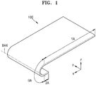
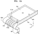
- FIGS. 1 and 2A are perspective views schematically illustrating a portion of a display apparatus, according to an exemplary embodiment.
- FIG. 2B is a plan view schematically illustrating a portion of a display apparatus, according to an exemplary embodiment.
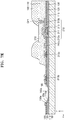
- FIG. 2C is a cross-sectional view schematically illustrating a portion of the display apparatus of FIG. 2A .
- a portion of the display apparatus according to the present exemplary embodiment is bent because a substrate 100 in the display apparatus is partially bent.
- FIG. 2C illustrates the display apparatus in a non-bent state.
- Cross-sectional views and plan views related to the exemplary embodiments disclosed below also illustrate the display apparatus in a non-bent state for convenience of description.
- the substrate 100 of the display apparatus is divided into a display area DA, in which a display device is provided and images are displayed, and a non-display area around the display area DA.
- the non-display area includes a bending area BA that is bent about a bending axis BAX.
- the bending area BA may refer to a bent area having a radius of curvature.
- the bending area BA extends in a first direction (+y direction) and is arranged between a first area 1A and a second area 2A in a second direction (+x direction) that intersects the first direction. Also, the substrate 100 is bent about the bending axis BAX that extends in the first direction (+y direction), as shown in FIG. 1 .
- the substrate 100 may include various flexible or bendable materials, for example, a polymer resin such as polyethersulfone (PES), polyacrylate (PAR), polyetherimide (PEI), polyethylene naphthalate (PEN), polyethylene terephthalate (PET), polyphenylene sulfide (PPS), polyarylate, polyimide (PI), polycarbonate (PC), or cellulose acetate propionate (CAP).
- a polymer resin such as polyethersulfone (PES), polyacrylate (PAR), polyetherimide (PEI), polyethylene naphthalate (PEN), polyethylene terephthalate (PET), polyphenylene sulfide (PPS), polyarylate, polyimide (PI), polycarbonate (PC), or cellulose acetate propionate (CAP).
- PES polyethersulfone
- PAR polyacrylate
- PEI polyetherimide
- PEN polyethylene naphthalate
- PET polyethylene terephthalate
- PPS
- the first area 1A includes the display area DA.
- the first area 1A may also include a portion of the non-display area around or outside the display area DA, as shown in FIG. 2C .
- the second area 2A also includes the non-display area.
- the display area DA may include, for example, a display device 300, a thin film transistor (TFT) 210, and a capacitor Cst (not shown).
- TFT thin film transistor
- the display area DA may further include a signal wiring including a gate line through which gate signals are transmitted, a data line through which data signals are transmitted, etc. that transfers a pulse signal and a direct current signal such as a driving power line, a common power line, etc (all not shown).
- a pixel may be formed and display an image based on an electric combination of the TFT, the capacitor, the display device, and the like connected to the gate line, the data line, and the driving power line.
- the brightness of the pixel may correspond to a driving current passing through the display device in response to the data signals according to the driving power and the common power supplied to the pixel.
- the signal wiring may be connected to a terminal unit 20 through a fan-out wiring 720a.
- the fan-out wiring 720a may transfer a pulse signal such as a gate signal, a data signal, etc. and a direct current such as power, etc.
- a pulse signal such as a gate signal, a data signal, etc.
- a direct current such as power, etc.
- a plurality of pixels may be provided and arranged in various ways, such as a stripe layout, a PenTileTM layout, or the like.
- the terminal unit 20, the fan-out wiring 720a, an additional conductive layer 215d, and a touch wire 720 may be arranged in the non-display area.
- a common power line, a driving power line, a gate driving unit, a data driving unit, etc. may be further arranged in the non-display area.
- the terminal unit 20 may be arranged in one end of the non-display area and may include a signal terminal 21 and a touch terminal 22.
- the terminal unit 20 may not be covered by an insulating layer but may be exposed so that the terminal unit 20 may be electrically connected to a driving circuit unit (not shown) such as a flexible printed circuit board (FPCB), a driver IC, etc.
- a control unit may provide a data signal, a gate signal, a driving voltage DLVDD, a common voltage ELVSS, etc.
- the control unit may also provide a signal to a touch screen layer 700 through the touch wire 720 or may receive a signal sensed by the touch screen layer 700.
- the fan-out wiring 720a is in the non-display area and connected to a TFT 210 in the display area DA or the first signal wiring 213b that applies electric signals to the display device 300.
- the first signal wiring 213b may correspond to various lines provided in the display area DA, such as the gate line, the data line, the driving power line, the common power line, or the like.
- the fan-out wiring 720a may be connected to the first signal wiring 213b and at least a portion of the fan-out wiring 720a may be in the bending area BA.
- the fan-out wiring 720a may extend from the first area 1A and be in a portion of the bending area BA, or extend across the bending area BA until the second area 2A.
- the fan-out wiring 720a may extend across the bending axis BAX.
- the fan-out wiring 720a may have various modifications, such as the fan-out wiring 720a may extend at a predetermined inclined angle with the bending axis BAX.
- the fan-out wiring 720a may have various shapes, such as a curved shape, a zigzag shape, etc. (other than a straight line shape).
- the fan-out wiring 720a may be connected to the signal terminal 21 of the terminal unit 20 to transfer an electrical signal to the display area DA.
- the additional conductive layer 215d may be further provided in the non-display area.
- the additional conductive layer 215d may be connected to a signal line applying an electrical signal to the TFT 210 or the display device 300 arranged in the display area DA, such as the fan-out wiring 720a.
- the additional conductive layer 215d may include a material different from the fan-out wiring 720a.
- the additional conductive layer 215d may include the same material as a gate line or a data line that is an internal signal line of the display area DA.
- the additional conductive layer 215d may be arranged in a different layer from the fan-out wiring 720a and, as shown in FIG. 2B , and may be horizontally spaced apart from the fan-out wiring 720a.
- the arrangement of the additional conductive layer 215d is not limited thereto.
- the additional conductive layer 215d may at least partially overlap with the fan-out wiring 720a.
- the additional conductive layer 215d may be electrically connected to the fan-out wiring 720a in a lower portion of the fan-out wiring 720a to apply an electrical signal to the display area DA.
- Another exemplary embodiment regarding a layout of the additional conductive layer 215d and the fan-out wiring 720a will be described below.
- the display apparatus may include a signal wiring 213b connected to the fan-out wiring 720a, in addition to the fan-out wiring 720a.
- the signal wiring 213b may be arranged in the first area 1A or the second area 2A in order to be located in a layer different from a layer in which the fan-out wring 720a, and may be electrically connected to the fan-out wring 720a.
- the signal wiring 213b may be electrically connected to a TFT 210 included in the display area DA and thus, the fan-out wiring 720a may be electrically connected to the TFT 210 included in the display area DA through the signal wiring 213b.
- the signal wiring 213b may be located outside the display area DA while electrically connected to components located in the display area DA, may be located outside the display area DA while extending in a direction of the display area DA, and thus, the signal wiring 213b may be at least partially located in the display area DA.
- the display area DA may be sealed by an encapsulation layer 400.
- the encapsulation layer 400 may cover the display device 300 and other elements in the display area DA and protect the display device 300 and other elements from external moisture or oxygen.
- the encapsulation layer 400 may cover the display area DA and partially extend to an outer portion of the display area DA.
- the touch screen layer 700 including a touch electrode 710 with various patterns for a touch screen function is provided.
- the touch electrode 710 may be connected to the touch wire 720 through which signals detected by the touch electrode 710 are transmitted.
- the touch wire 720 may extend from an upper portion of the encapsulation layer 400 to the non-display area along a side of the encapsulation layer 400.
- the touch wire 720 may be connected to the touch screen layer 700, and extend from the upper portion of the encapsulation layer 400 until at least a portion of the touch wire 720 is in the bending area BA.
- FIG. 2C illustrates a display device 300 in the form of an organic light-emitting device in the display area DA.
- the organic light-emitting device 300 being electrically connected to the TFT 210 may indicate that a pixel electrode 310 is electrically connected to the TFT 210.
- another TFT (not shown) may be provided in a surrounding area outside the display area DA of the substrate 100.
- the TFT provided in the surrounding area may be, for example, a portion of a circuit unit for controlling electric signals applied to the display area DA.
- the TFT 210 may include a semiconductor layer 211 including non-amorphous silicon, polycrystalline silicon, an oxide semiconductor material, or an organic semiconductor material.
- the TFT 210 may also include a gate electrode 213, a source electrode 215a, and a drain electrode 215b.
- the gate electrode 213 may be connected to a gate line (not shown) that applies on and off signals to the TFT 210.
- the gate electrode 213 may include a low-resistive metallic material.
- the gate electrode 213 may be a single layer or layers formed of a conductive material including, for example, molybdenum (Mo), aluminum (Al), copper (Cu), and/or titanium (Ti).
- Each of the source electrode 215a and the drain electrode 215b may be a single layer or layers including a conductive material.
- the source electrode 215a and the drain electrode 215b may be respectively connected to a source area and a drain area of the semiconductor layer 211.
- each of the source electrode 215a and the drain electrode 215b may be a single layer or layers formed of a conductive material including, for example, Al, Cu, and/or Ti.
- the TFT 210 may be a top gate type TFT in which the gate electrode 213 is above the semiconductor layer 211. However, other exemplary embodiments of the TFT 210 are not limited thereto.
- the TFT 210 according to another exemplary embodiment may be a bottom gate type TFT in which the gate electrode 213 is under the semiconductor layer 211.
- a gate insulating layer 120 may be provided between the semiconductor layer 211 and the gate electrode 213, the gate insulating layer 120 including an inorganic material, such as silicon oxide, silicon nitride, and/or silicon oxynitride,.
- an interlayer insulating layer 130 may be provided above the gate electrode 213, the interlayer insulating layer 130 including an inorganic material such as silicon oxide, silicon nitride, and/or silicon oxynitride.
- the source electrode 215a and the drain electrode 215b may be provided above the interlayer insulating layer 130.
- An insulating layer including an inorganic material may be formed through chemical vapor deposition (CVD) or atomic layer deposition (ALD). This also applies to exemplary embodiments described below and modified examples of the exemplary embodiments.
- a buffer layer 110 may be provided between the TFT 210 and the substrate 100, the buffer layer 110 including an inorganic material such as silicon oxide, silicon nitride, and/or silicon oxynitride.
- the buffer layer 110 may planarize an upper surface of the substrate 100 or prevent impurities from the substrate 100 penetrating into the semiconductor layer 211 of the TFT 210.
- the buffer layer 110 may have a single layer structure or a multiple layer structure.
- a planarization layer 140 may be disposed above the TFT 210.
- the planarization layer 140 may planarize an upper portion of a protection layer that covers the TFT 210.
- the planarization layer 140 may include an organic material, for example, PI, acryl, benzocyclobutene (BCB), or hexamethyldisiloxane (HMDSO).
- FIG. 2C illustrates the planarization layer 140 as a single layer, the planarization layer 140 may be layers or modified in other various ways.
- the organic light-emitting device may be disposed on the planarization layer 140.
- the organic light-emitting device may include the pixel electrode 310, an opposite electrode 330, and an intermediate layer 320 that is provided between the pixel electrode 310 and the opposite electrode 330 and includes an emission layer.
- the pixel electrode 310 may be electrically connected to the TFT 210 by contacting any one of the source electrode 215a and the drain electrode 215b through an opening formed in the planarization layer 140.
- a pixel defining layer 150 may be disposed above the planarization layer 140.
- the pixel defining layer 150 defines a pixel with openings that respectively correspond to subpixels, i.e., openings that expose at least a central portion of the pixel electrode 310.
- the pixel defining layer 150 on the pixel electrode 310 may increase a distance between a periphery of the pixel electrode 310 and the opposite electrode 330 so that an arc is not created at the periphery of the pixel electrode 310.
- the pixel defining layer 150 may include, for example, PI, acryl, BCB, or HMDSO.
- the intermediate layer 320 of the organic light-emitting device may include a low molecular material or a high molecular material.
- the intermediate layer 320 may include an emission layer (EML), and may further include at least one of a hole injection layer (HIL), a hole transport layer (HTL), an electron transport layer (ETL), and an electron injection layer (EIL).
- the intermediate layer 320 may include various organic materials, for example, copper phthalocyanine (CuPc), N,N'-Di(naphthalene-1-yl)-N,N'-diphenyl-benzidine (NPB), tris-8-hydroxyquinoline aluminum (Alq 3 ), or the like.
- the layers may be formed by vapor deposition.
- the intermediate layer 320 may include an HTL and an EML.
- the HTL may include PEDOT
- the EML may include poly-phenylenevinylene (PPV) based and polyfluorene-based high molecular materials.
- the intermediate layer 320 may be formed by screen printing, inkjet printing, laser induced thermal imaging (LITI), or the like.
- the intermediate layer 320 is not limited to the above examples.
- the intermediate layer 320 may include a single layer across a plurality of pixel electrodes 310, or layers that are patterned with respect to each of the pixel electrodes 310.
- the opposite electrode 330 is in an upper portion of the display area DA. As shown in FIG. 2 , the opposite electrode 330 may be provided to cover the display area DA. That is, the opposite electrode 330 may be formed as a single element for a plurality of organic light-emitting devices and thus, correspond to the plurality of pixel electrodes 310.
- the encapsulation layer 400 may cover and protect the organic light-emitting device.
- the encapsulation layer 400 may cover a pixel area and extend to an outer area of the pixel area. As shown in FIG. 2C , the encapsulation layer 400 may include a first inorganic encapsulation layer 410, an organic encapsulation layer 420, and a second inorganic encapsulation layer 430.
- the first inorganic encapsulation layer 410 may cover the opposite electrode 330, and include silicon oxide, silicon nitride, and/or silicon oxynitride. If necessary, other layers, such as a capping layer, may be provided between the first inorganic encapsulation layer 410 and the opposite electrode 330. Since the first inorganic encapsulation layer 410 is formed along its lower structure, an upper surface of the first inorganic encapsulation layer 410 is not flat, as shown in FIG. 2C . Unlike the first inorganic encapsulation layer 410, the organic encapsulation layer 420 covering the first inorganic encapsulation layer 410 may have a flat upper surface.
- an upper surface of the organic encapsulation layer 420 corresponding to the display area DA may be substantially flat.
- the organic encapsulation layer 420 may include at least one selected from the group consisting of PET, PEN, PC, PI, PES, polyoxymethylene (POM), polyarylate, and HMDSO.
- the second inorganic encapsulation layer 430 may cover the organic encapsulation layer 420, and include silicon oxide, silicon nitride, and/or silicon oxynitride. A periphery of the second inorganic encapsulation layer 430 outside the display area DA may contact the first inorganic encapsulation layer 410 so that the organic encapsulation layer 420 is not externally exposed.
- the encapsulation layer 400 has a multi-layer structure including the first inorganic encapsulation layer 410, the organic encapsulation layer 420, and the second inorganic encapsulation layer 430, even when there is a fracture in the encapsulation layer 400, the fracture does not extend between the first inorganic encapsulation layer 410 and the organic encapsulation layer 420 or between the organic encapsulation layer 420 and the second inorganic encapsulation layer 430. Accordingly, external moisture or oxygen may be prevented from penetrating into the display area DA.
- the touch screen layer 700 includes the touch electrode 710 is provided above the encapsulation layer 400.
- a cover layer 730 may be provided above the touch screen layer 700 and protect the touch screen layer 700.
- the touch screen layer 700 may be, for example, a capacitance type. When the cover layer 730 is touched, whether a portion is touched may be determined by detecting a change in the mutual capacitance formed between touch electrodes 710 of the touch screen layer 700. Alternatively, the, touch screen layer 700 may determine whether a portion is touched by detecting a change in the capacitance between the touch electrode 710 and the opposite electrode 330, or by other techniques.
- the touch electrode 710 may be connected to the touch wire 720 that transmits signals detected by the touch electrode 710, the touch wire 720 may extend from the upper portion of the encapsulation layer 400 to the non-display area along a side of the encapsulation layer 400.
- the touch wire 720 may be connected to the touch screen layer 700, and extend from the upper portion of the encapsulation layer 400 until at least a portion of the touch wire 720 is in the bending area BA.
- the touch wire 720 may be arranged across the bending area BA.
- the touch wire 720 may extend from the encapsulation layer 400 along a side of the encapsulation layer 400, and in this case, the side of the encapsulation layer 400 may be curved.
- the curve may be formed due to a stair-step formed by the planarization layer 140 and the pixel defining layer 150, as shown in FIG. 2C .
- the touch wire 720 may extend from the upper portion of the encapsulation layer 400 to a non-sealed area with a gradual slope.
- Each of the touch electrode 710 and the touch wire 720 may be a single layer or layers including a conductive material, for example, Al, Cu, and/or Ti.
- the touch electrode 710 and the touch wire 720 may include an identical material.
- the cover layer 730 may be flexible, and include, for example, polymethyl methacrylate, polydimethylsiloxane, PI, acrylate, PET, PEN, or the like.
- the cover layer 730 may be arranged above the touch screen layer 700 to protect the touch screen layer 700.
- a touch buffer layer 610 may be provided between the encapsulation layer 400 and the touch screen layer 700.
- the touch buffer layer 610 may prevent damage to the encapsulation layer 400, and block interference signals that may be generated when the touch screen layer 700 is operated.
- the touch buffer layer 610 may include an inorganic material, such as silicon oxide, silicon nitride, silicon oxynitride, aluminum oxide, aluminum nitride, titanium oxide, titanium nitride, or the like, or an organic material such as PI, polyester, acryl, or the like. Also, the touch buffer layer 610 may be formed by stacking layers of the aforementioned materials.
- the touch buffer layer 610 may be directly formed on the encapsulation layer 400 by deposition or using other methods. Since the touch screen layer 700 is also formed directly on the touch buffer layer 610, an additional attachment layer is unnecessary on the encapsulation layer 400. Therefore, a thickness of the display apparatus may be reduced.
- the non-display area may include the bending area BA.
- the fan-out wiring 720a may be provided across the bending area BA in the non-display area.
- the fan-out wiring 720a may be electrically connected to the TFT 210 or the first signal wiring 213b, a second signal wiring 213c, and a third signal wiring 215c that apply electrical signals to the display device 300, which are provided in the display area DA.
- the fan-out wiring 720a being electrically connected to the first, second, and third signal wirings 213b, 213c, and 215c not only indicates that the fan-out wiring 720a is directly connected to the first signal wiring 213b through a contact hole as shown in FIG. 2C , but also indicates that the fan-out wiring 720a is indirectly connected to the second signal wiring 213c or the third signal wiring 215c via the first signal wiring 213b.
- the first signal wiring 213b may be electrically connected to the second signal wiring 213c or the third signal wiring 215c in the display area DA.
- the second signal wiring 213c or the third signal wiring 215c may be a gate line that applies signals to the gate electrode 213.
- the second signal wiring 213c or the third signal wiring 215c may be a data line that applies signals to the source electrode 215a or the drain electrode 215b.
- the first signal wiring 213b may be connected to the second signal wiring 213c through a via hole.
- the first signal wiring 213b and the second signal wiring 213c may include the same material as the gate electrode 213.
- the third signal wiring 215c may include the same material as the source electrode 215a and the drain electrode 215b.
- the fan-out wiring 720a may include the same material as the touch wire 720.
- the fan-out wiring 720a and the touch wire 720 may be simultaneously formed under an identical manufacturing condition.
- the fan-out wiring 720a and the touch wire 720 may include Al.
- the fan-out wiring 720a and the touch wire 720 may include Ti/Al/Ti.
- the fan-out wiring 720a may include the same material as the touch wire 720, but a different material from the first signal wiring 213b, the second signal wiring 213c, the third signal wiring 215c, the source electrode 215a, or the drain electrode 215b.
- the fan-out wiring 720a may include the same material as the first signal wiring 213b, the second signal wiring 213c, the third signal wiring 215c, the source electrode 215a, or the drain electrode 215b.
- the fan-out wiring 720a and the touch wire 720 may be formed by a low-temperature layer formation process at about 90°C or below. This may be to protect the display device 300 or other elements that are already formed.
- the first signal wiring 213b, the second signal wiring 213c, the third signal wiring 215c, the source electrode 215a, and the drain electrode 215b may be formed by a high-temperature layer formation process at a temperature that is equal to or higher than 90°C, for example, about 150°C, in which the first signal wiring 213b, the second signal wiring 213c, the third signal wiring 215c, the source electrode 215a, and the drain electrode 215b are formed before the display device 300, the encapsulation layer 400, or another element is formed.
- respective resistivity values Whereby resistivity especially means the electrical resistivity when used herein
- respective grain sizes may vary.
- a resistance value of the fan-out wiring 720a may be about 25% greater than a resistance value of the first, second, and third signal wirings 213b, 213c, and 215c.
- a grain size of the fan-out wiring 720a may be smaller than a grain size of the first, second, and third signal wirings 213b, 213c, and 215c.
- respective thicknesses of the fan-out wiring 720a and the first, second, and third signal wirings 213b, 213c, and 215c may be different from one another.
- a thickness of the fan-out wiring 720a may be less than a thickness of the third signal wiring 215c that is formed by using the same material as the source electrode 215a and the drain electrode 215b.
- the thickness of the fan-out wiring 720a may be about 50% of the thickness of the third signal wiring 215c.
- An organic material layer 160 may be provided in at least a portion of the bending area BA between the fan-out wiring 720a and the substrate 100.
- the organic material layer 160 may prevent fractures in the fan-out wiring 720a of the bending area BA when the display apparatus is bent.
- the organic material layer 160 may absorb tensile stress of the substrate 100 and other elements, caused by bending, to thus effectively reduce tensile stress concentrated on the fan-out wiring 720a.
- the organic material layer 160 may be formed by using the same material and at the same time as the planarization layer 140, the pixel defining layer 150, the organic encapsulation layer 420 of the encapsulation layer 400, or the touch buffer layer 610. That is, the organic material layer 160 may be formed during a mask process for forming the planarization layer 140, the pixel defining layer 150, the organic encapsulation layer 420 of the encapsulation layer 400, or the touch buffer layer 610. Accordingly, an additional mask process for forming the organic material layer 160 may be omitted.
- the buffer layer 110, the gate insulating layer 120, or the interlayer insulating layer 130 may also include an organic material. In this case, the organic material layer 160 may be formed by using the same material and at the same time as the buffer layer 110, the gate insulating layer 120, or the interlayer insulating layer 130.
- the fan-out wiring 720a is formed at the same time as the first signal wiring 213b, the second signal wiring 213c, the third signal wiring 215c, the source electrode 215a, or the drain electrode 215b, an additional mask has to be used to form the organic material layer 160.
- the organic material layer 160 may be formed together with a layer including an organic material provided in the display area DA, which thus simplifies the mask process.
- the buffer layer 110, the gate insulating layer 120, and the interlayer insulating layer 130, all of which include an inorganic material, may be referred to as an inorganic insulating layer.
- the inorganic insulating layer may have an opening corresponding to the bending area BA as shown in FIG. 2C . That is, the buffer layer 110, the gate insulating layer 120, and the interlayer insulating layer 130 may respectively have openings 110a, 120a, and 130a that correspond to the bending area BA.
- An opening corresponding to the bending area BA may indicate that the opening overlaps the bending area BA.
- the opening may be larger than the bending area BA. Accordingly, FIG. 2C shows that a width OW of the opening is greater than a width of the bending area BA.
- the smallest from among the respective openings 110a, 120a, and 130a of the buffer layer 110, the gate insulating layer 120, and the interlayer insulating layer 130 may be determined as a size of the opening.
- the size of the opening 110a of the buffer layer 110 is determined as the size of the opening.
- the display apparatus includes the organic material layer 160 that fills at least a portion of the opening of the inorganic insulating layer.
- FIG. 2C shows that the organic material layer 160 totally fills the opening.
- the fan-out wiring 720a may extend across the bending area BA from the first area 1A to the second area 2A, and may be on the organic material layer 160. In areas where the organic material layer 160 is not provided, the fan-out wiring 720a may be on the inorganic insulating layer, such as the interlayer insulating layer 130.
- the inorganic insulating layer in the bending area BA is likely to have fractures.
- the inorganic insulating layer fractures, there is a high probability that the fractures may occur in the fan-out wiring 720a.
- the organic material layer 160 may block the fractures from spreading, the opening formed in the inorganic insulating layer may further reduce the probability of the occurrence of fractures in the inorganic insulating layer. Therefore, a reduced level of tensile stress may concentrate on the fan-out wiring 720a.
- the organic material layer 160 may cover an inner surface of the opening of the inorganic insulating layer.
- Various wires of the display apparatus may be formed by forming a conductive material layer on an entire surface of the substrate 100 and patterning the conductive material layer.
- the organic material layer 160 does not cover an inner surface of the opening 110a of the buffer layer 110, an inner surface of the opening 120a of the gate insulating layer 120, or an inner surface of the opening 130a of the interlayer insulating layer 130, during the patterning of the conductive material layer, a conductive material may not be removed from but may instead remain in the inner surface of the opening 110a of the buffer layer 110, the inner surface of the opening 120a of the gate insulating layer 120, or the inner surface of the opening 130a of the interlayer insulating layer 130. In this case, the remaining conductive material may cause a short circuit between conductive layers. Therefore, the organic material layer 160 may be formed to cover the inner surface of the opening of the inorganic insulating layer.
- the organic material layer 160 has a uniform thickness for reference, alternatively, the organic material layer 160 may have different thicknesses according to various locations so that the organic material layer 160 gradually rises and falls around the inner surface of the opening 110a of the buffer layer 110, the inner surface of the opening 120a of the gate insulating layer 120, or the inner surface of the opening 130a of the interlayer insulating layer 130.
- the display apparatus may further include a protection film 170.
- the protection film 170 may be a lower protection film protecting a lower surface of the substrate 100 and, as shown in FIG. 2C , may have an opening 170OP.
- the opening 170OP may correspond to the bending area BA.
- An area of the opening 170OP may be greater than that of the bending area BA.
- a width of the opening 170OP may be greater than that of the bending area BA.
- the protection film 170 may protect the lower surface of the substrate 100 and thus, having rigidity itself. Accordingly, when the protection film 170 has a low flexibility, since the substrate 100 is bent, the protection film 170 may be separated from the substrate 100. Thus, as shown in FIG. 2C , the protection film 170 may have the opening 170OP corresponding to the bending area BA, thereby effectively preventing the protection film 170 from being separated from the substrate 100. To this end, as described above, the area of the opening 170OP of the protection film 170 may be greater than that of the bending area BA. In FIG. 2C , the protection film 170 is removed from the bending area BA but is not limited thereto. The protection film 170 may be variously modified, for example, the protection film 170 may not be completely removed from the bending area BA but may have a small thickness in the bending area BA compared to the first area 1A or the second area 2A.
- a bending protection layer (BPL) 600 may be located outside the display area DA. That is, the BPL 600 may correspond to at least the bending area BA to be located above the fan-out wiring 720a.
- a stress neutral plane may be present in the stack structure. If the BPL 600 is not present, an excessive tensile stress may be applied to the fan-out wiring 720a in the bending area BA according to bending of the substrate 100 because a location of the fan-out wiring 720a may not correspond to the stress neutral plane. However, by allowing the BPL 600 to be present and adjusting a thickness and a modulus of the BPL 600, a location of the stress neutral plane in a stack structure including all the substrate 100, the fan-out wiring 720a, and the BPL 600 may be adjusted. Thus, the stress neutral plane may be located near the fan-out wiring 720a through the BPL 600, and thus less tensile stress may be applied to the fan-out wiring 720a.
- a top surface in a direction (-x direction) toward the display area DA of the BPL 600 coincides with a top surface in a direction (+z direction) of the cover layer 730, but the present invention is not limited thereto.
- an end of the BPL 600 in the direction (the -x direction) toward the display area DA may partially cover a top surface at an edge of the cover layer 730.
- various modification may be possible, for example, the end of the BPL 600 in the direction (the -x direction) toward the display area DA may not contact the cover layer 730.
- the BPL 600 may extend to an upper portion of the display area DA to cover the touch electrode 710.
- the BPL 600 may be formed by applying and hardening a liquid phase material or a paste-type material. In this case, a volume of the BPL 600 may be reduced during a hardening process. In this regard, when a portion of the BPL 600 in the direction (-x direction) toward the display area DA is in contact with the cover layer 730, a location of the portion of the BPL 600 is fixed, and thus, volume reduction occurs in a remaining portion of the BPL 600. As a result, a thickness of the portion of the BPL 600 in the direction (-x direction) toward the display area DA may be greater than those of other portions of the BPL 600.
- the BPL 600 may expose the signal terminal 21 (see FIG. 2B ) of the second area 2A.
- the signal terminal 21 may be used to connect a control unit such as various electronic elements or a PCB, etc.
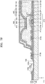
- FIG. 3A is a cross-sectional view schematically illustrating a portion of a display apparatus according to another exemplary embodiment.
- the cover layer 730 may extend to a non-display area from an upper portion of the touch screen layer 700 to cover the fan-out wiring 720a. Accordingly, the cover layer 730 may simultaneously protect the touch screen layer 700 and the fan-out wiring 720a.
- the cover layer 730 may extend as one piece from the display area DA to at least the bending area BA.
- the cover layer 730 may function as the BPL 600 (see FIG. 2C ). That is, the cover layer 730 may adjust a location of a stress neutral plane in the bending area BA. The stress neutral plane may be located near the fan-out wiring 720a through the cover layer 730, and thus, a reduced level of tensile stress may be applied to the fan-out wiring 720a.
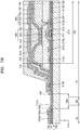
- FIG. 3B is a cross-sectional view schematically illustrating a portion of a display apparatus according to another exemplary embodiment.
- the cover layer 730 may extend to a non-display area from an upper portion of the touch screen layer 700 to cover the fan-out wiring 720a. That is, the cover layer 730 may extend as one piece from the display area DA to at least the bending area BA.
- the BPL 600 may be further provided over the cover layer 730 in the non-display area.
- the BPL 600 as described above, may be used to apply a reduced level of tensile stress to the fan-out wiring 720a by locating a stress neutral plane near the fan-out wiring 720a.
- the cover layer 730 extends to the bending area BA, but the present invention is not limited thereto.
- the BPL 600 may be arranged in the bending area BA, instead of the cover layer 730, the cover layer 730 and the BPL 600 may be simultaneously arranged or neither of them may be arranged.
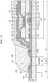
- FIG. 4A is a cross-sectional view schematically illustrating a portion of a display apparatus according to another exemplary embodiment.
- the touch electrode 710 may be formed by sequentially stacking a first touch conductive layer 711, a first insulating layer 712, a second touch conductive layer 713, and a second insulating layer 714.
- the first touch conductive layer 711 may be electrically connected to the second touch conductive layer 713.
- the first insulating layer 712 may include a via hole that exposes an upper surface of the first touch conductive layer 711, and the first touch conductive layer 711 may be connected to the second touch conductive layer 713 through the via hole.
- resistance of the touch electrode 710 may decrease, and thus the response speed of the touch screen layer 700 may increase.
- the fan-out wiring 720a and the touch wire 720 may include the same material as the first touch conductive layer 711 or the second touch conductive layer 713. In other exemplary embodiments, the fan-out wiring 720a and the touch wire 720 may have a structure in which a first layer including the same material as the first touch conductive layer 711, and a second layer including the same material as the second touch conductive layer 713, are stacked.
- the touch wire 720 may include the same material as the first touch conductive layer 711 or the second touch conductive layer 713. In other exemplary embodiments, the touch wire 720 may be formed by stacking a first layer including the same material as the first touch conductive layer 711 and a second layer including layer including the same material as the second touch conductive layer 713.
- Each of the first touch conductive layer 711 and the second touch conductive layer 713 may be a single layer or layers formed of a conductive material, for example, Al, Cu, and/or Ti.
- each of the first touch conductive layer 711 and the second touch conductive layer 713 may have a stack structure formed of Ti/Al/Ti.
- the first insulating layer 712 may include an inorganic material or an organic material.
- the inorganic material may include at least one selected from silicon nitride, aluminum nitride, zirconium nitride, titanium nitride, hafnium nitride, tantalum nitride, silicon oxide, aluminum oxide, titanium oxide, tin oxide, cerium oxide, and silicon oxynitride.
- the organic material may include at least one selected from an acryl-based resin, a methacryl-based resin, polyisoprene, a vinyl-based resin, an epoxy-based resin, a urethane-based resin, a cellulose-based resin, and a perylene-based resin.
- the second insulating layer 714 may include an organic material, for example, at least one selected from an acryl-based resin, a methacryl-based resin, polyisoprene, a vinyl-based resin, an epoxy-based resin, a urethane-based resin, a cellulose-based resin, and a perylene-based resin.
- the organic material layer 160 may be simultaneously formed with the first insulating layer 712 or the second insulating layer 714 by using the same material as the first insulating layer 712 or the second insulating layer 714.
- the organic material layer 160 may be simultaneously formed with the planarization layer 140, the pixel defining layer 150, the organic encapsulation layer 420 of the encapsulation layer 400, the touch buffer layer 610, the first insulating layer 712 or the second insulating layer 714 by using the same material as the planarization layer 140, the pixel defining layer 150, the organic encapsulation layer 420 of the encapsulation layer 400, the touch buffer layer 610, the first insulating layer 712 or the second insulating layer 714 but the present invention is not limited thereto.
- the organic material layer 160 may be formed through a process different from a process forming the planarization layer 140, the pixel defining layer 150, the organic encapsulation layer 420 of the encapsulation layer 400, the touch buffer layer 610, the first insulating layer 712 or the second insulating layer 714.
- the buffer layer 110, the gate insulating layer 120 and/or the interlayer insulating layer 130 may include an organic material.
- the organic material layer 160 may be formed by using the same material as the buffer layer 110, the gate insulating layer 120, or the interlayer insulating layer 130.
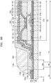
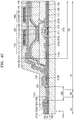
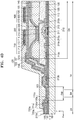
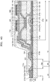
- FIGS. 4B and 4C are cross-sectional views schematically illustrating a portion of a display apparatus according to another exemplary embodiment.
- the display apparatus according to the present exemplary embodiment is different from a display apparatus according to the above-described exemplary embodiment in that the additional conductive layer 215d may be further provided in a lower portion of the fan-out wiring 720a.
- the additional conductive layer 215d may be simultaneously formed with the source electrode 215a or the drain electrode 215b by using the same material as the source electrode 215a or the drain electrode 215b.
- the additional conductive layer 215d may be located in a lower portion of the fan-out wiring 720a at least in the bending area BA such that the additional conductive layer 215d is electrically connected to the fan-out wiring 720a.
- a conductive layer of the bending area BA may have a multiple layer structure.
- an electric signal may be transferred to the display area DA by the additional conducive layer 215d without a problem.
- an electric signal may be transferred to the display area DA by the fan-out wiring 720a without a problem.
- the fan-out wiring 720a and the touch wire 720 may include the same material as the first touch conductive layer 711 as shown in FIG. 4B or may include the same material as the second touch conducive layer 713 as shown in FIG. 4C .
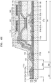
- FIG. 4D is a cross-sectional view schematically illustrating a portion of a display apparatus according to another exemplary embodiment.
- the display apparatus according to the present exemplary embodiment is different from a display apparatus described with reference to FIG. 4B in that the fan-out wiring 720a has a structure in which a first layer 721a including the same material as the first touch conductive layer 711, and a second layer 723a including the same material as the second touch conductive layer 713, are stacked.
- the touch wire 720 may have a structure in which a first wire layer 721 including the same material as the first touch conductive layer 711, and a second wire layer 723 including the same material as the second touch conductive layer 713, are stacked.
- the display apparatus since the display apparatus according to the present exemplary embodiment includes a conductive layer having a multiple layer structure in the bending area BA, even if a crack occurs in a conductive layer having a single layer structure, an electrical signal may be transferred to the display area DA without a problem.
- FIG. 4E is a cross-sectional view schematically illustrating a portion of a display apparatus according to another exemplary embodiment.
- the additional conductive layer 215d may be arranged in a lower portion of the fan-out wiring 720a.
- the additional conductive layer 215d may be formed by the first signal wiring 213b extending across the bending area BA. That is, the additional conductive layer 215d may include the same material as the gate electrode 213.
- the additional conductive layer 215d may directly contact the fan-out wiring 720a in the bending area BA to form a multiple layer structure.
- a conductive layer of the bending area BA may have a multiple layer structure.
- an electric signal may be transferred to the display area DA by the additional conducive layer 215d without a problem.
- an electric signal may be transferred to the display area DA by the fan-out wiring 720a without a problem.
- the fan-out wiring 720a may include the same material as the first touch conductive layer 711 or the second touch conducive layer 713.
- the fan-out wiring 720a may have a structure in which a first layer including the same material as the first touch conductive layer 711 and a second layer including the same material as the second touch conductive layer 713 are stacked.
- FIGS. 4F and 4G are cross-sectional views schematically illustrating a portion of a display apparatus according to another exemplary embodiment.
- the display apparatus may include the additional conductive layer 215d in a lower portion of the fan-out wiring 720a in the bending area BA and an insulating layer 180 between the fan-out wiring 720a and the additional conductive layer 215d.
- the fan-out wiring 720a may be simultaneously formed with the touch wire 720 by using the same material as the touch wire 720, and the additional conductive layer 215d may be simultaneously formed with the source electrode 215a, the drain electrode 215b, or the gate electrode 213 by using the same material as the source electrode 215a, the drain electrode 215b, or the gate electrode 213.
- the additional conductive layer 215d may be electrically connected to the fan-out wiring 720a through a via hole provided in the insulating layer 180.
- the via hole may be arranged in the first area 1A and/or the second area 2A.
- the additional conductive layer 215d and the fan-out wiring 720a may have various modifications, for example, the additional conductive layer 215d and the fan-out wiring 720a may be arranged over the bending area BA or may overlap only in a part of the bending area BA as described in the above-described exemplary embodiments.
- the insulating layer 180 may include an organic material or an inorganic material.
- the insulating layer 180 may be simultaneously formed with the planarization layer 140, the pixel defining layer 150, the inorganic encapsulation layers 410 and 430 of the encapsulation layer 400, the organic encapsulation layer 420, the touch buffer layer 610, etc. by using the same material as the planarization layer 140, the pixel defining layer 150, the inorganic encapsulation layers 410 and 430 of the encapsulation layer 400, the organic encapsulation layer 420, the touch buffer layer 610, etc.
- the additional conductive layer 215d may be present only in a part of the bending area BA.
- the additional conductive layer 215d may be present in both edges of the bending area BA to contact the fan-out wiring 720a.
- the additional conductive layer 215d may have various modifications, for example, the additional conductive layer 215d may be present in only one edge of the bending area BA.
- FIG. 4H is a cross-sectional view schematically illustrating a portion of a display apparatus according to another exemplary embodiment.
- the fan-out wiring 720a may be present only in a part of the bending area BA.
- the fan-out wiring 720a may be present in both edges of the bending area BA to contact the additional conductive layer 215d.
- the fan-out wiring 720a may have various modifications, for example, the fan-out wiring 720a may be present in only one edge of the bending area BA.
- FIG. 4I is a cross-sectional view schematically illustrating a portion of a display apparatus according to another exemplary embodiment.
- the display apparatus may include a second TFT 210' in the display area DA, in addition to the TFT 210.
- the TFT 210' may include a semiconductor layer 211', a source electrode 215a', a drain electrode 215b', and a gate electrode 213'.
- the semiconductor layer 211' may include the same material as the semiconductor layer 211, and may be located on the same layer as the semiconductor layer 211.
- the source electrode 215a' and the drain electrode 215b' may also include the same materials as the source electrode 215a and the drain electrode 215b and may be located in the same layer as the source electrode 215a and the drain electrode 215b.
- the gate electrode 213' may be located in a different layer from the gate electrode 213, which may indicate that the gate electrode 213' and the gate electrode 213 are not simultaneously formed and are formed in different operations.
- a gate insulating layer 120' may be located above the gate insulating layer 120, and the source electrode 215a, the drain electrode 215b, the source electrode 215a', and the drain electrode 215b' may be located above the interlayer insulating layer 130 covering the gate insulating layer 120'.
- the gate electrode 213 may be located above the gate insulating layer 120.
- the gate insulating layer 120' may cover the gate electrode 213.
- the gate electrode 213' may be located above the gate insulating layer 120'.
- a wire arranged in the same layer as the gate electrode 213' and/or an electrode of a capacitor (not shown) arranged in the same layer as the gate electrode 213' may be added.
- various modifications may be possible, for example, the TFT 210' may be omitted.
- the display apparatus may further include a first additional conductive layer 215d' and/or a second additional conductive layer 215d" in the bending area BA.
- the first additional conductive layer 215d' may include the same material as the gate electrode 213 and may be arranged in the same layer as the gate electrode 213.
- the second additional conductive layer 215d" may include the same material as the gate electrode 213' and may be arranged in the same layer as the gate electrode 213'.
- the first additional conductive layer 215d' and/or the second additional conductive layer 215d" may extend over the bending area BA and may be arranged in a lower portion of the fan-out wiring 720a in the bending area BA.
- the first additional conductive layer 215d', the second additional conductive layer 215d", and the fan-out wiring 720a may be sequentially stacked in the bending area BA to form a multiple layer structure.
- an electric signal may be transferred to the display area DA by the first additional conductive layer 215d' and/or the second additional conductive layer 215d" without a problem.
- an electric signal may be transferred to the display area DA by the fan-out wiring 720a without a problem.
- the present invention is not limited thereto.
- the first additional conductive layer 215d', the second additional conductive layer 215d", and/or the fan-out wiring 720a may be arranged over the bending area BA or may overlap only in a part of the bending area BA as described in the above-described embodiments.
- the first additional conductive layer 215d' and the fan-out wiring 720a may overlap in a part of the bending area BA, and the second additional conductive layer 215d" and the fan-out wiring 720a may overlap in another part of the bending area BA.
- the first additional conductive layer 215d' and/or the second additional conductive layer 215d" may not overlap with the fan-out wiring 720a and only the first additional conductive layer 215d' and/or the second additional conductive layer 215d" may be arranged in a part of the bending area BA.
- the insulating layers 180 may be arranged between layers of each of the first additional conductive layers 215d', the second additional conductive layers 215d", and the fan-out wirings 720a.
- FIGS. 5A through 5I are cross-sectional views schematically illustrating a portion of a display apparatus according to an exemplary embodiment.
- FIGS. 5A to 5G are cross-sectional view that illustrate a region near the bending area BA.
- a height h1 of at least a portion of the organic material layer 160 in the opening of the inorganic insulating layer may be greater than a height h2 of the inorganic insulating layer.
- a height of a central portion of the organic material layer 160 may be greater than the heights at both ends of the opening.
- the organic material layer 160 may cover the inner surface of the opening such that a short circuit does not occur between the fan-out wiring 720a and a conductive material remaining on the inner surface of the opening.
- the height h1 of the organic material layer 160 in the opening of the inorganic insulating layer may be substantially a height h2 of the inorganic insulating layer.
- the organic material layer 160 may cover the inner surface of the opening such that a short does not occur between the fan-out wiring 720a and the conductive material remaining on the inner surface of the opening.
- the height h1 of the organic material layer 160 may vary depending on tensile stress due to the bending.
- an upper surface (in a +z direction) of the organic material layer 160 in the opening of the inorganic insulating layer may have some degree of surface unevenness. Accordingly, a surface area of an upper surface of the organic material layer 160 and surface areas of upper and lower surfaces of the fan-out wiring 720a in the opening may increase.
- the surface area increase of the upper surface of the organic material layer 160 and the upper and lower surfaces of the fan-out wiring 720a may denote that a deformation margin increases in order to reduce tensile stress due to the bending of the substrate 100.
- the lower surface of the fan-out wiring 720a may be shaped to correspond to unevenness surfaces 160a of the organic material layer 160.
- the unevenness surfaces 160a of the upper surface (in the +z direction) of the organic material layer 160 may be formed by using various methods.
- a photosensitive material may be used when forming the organic material layer 160, and during the manufacturing process, the amount of light exposure may be differentiated by using a slit mask or a halftone mask in various portions of the organic material layer 160 that still have a substantially flat upper surface.
- a certain portion may be relatively more etched (removed) than other portions.
- the portion that is relatively more etched may be a portion that is concave with respect to the upper surface of the organic material layer 160.
- Methods of manufacturing the display apparatus according to the present exemplary embodiment are not limited to the aforementioned method. For example, dry etching a certain portion after forming the organic material layer 160 with a substantially flat upper surface, or other various methods may be used.
- the organic material layer 160 may cover the inner surface of the opening and extend to a portion of an upper surface of the inorganic insulating layer.
- the organic material layer 160 may not be disposed in at least a portion of the central portion of the opening.
- the organic material layer 160 may cover the inner surface of the opening to prevent a short between the fan-out wiring 720a and a conductive material remaining on the inner surface of the opening. According to the present exemplary embodiment, since there is no inorganic insulating layer in the bending area BA, there is a lower probability of the formation of fractures in the fan-out wiring 720a.
- the inorganic insulating layer may have a groove in the bending area BA instead of an opening that exposes the substrate 100.
- only a portion of the inorganic insulating layer i.e., only a portion of the buffer layer 110, the gate insulating layer 120, and the interlayer insulating layer 130, may be removed in the bending area BA.
- the buffer layer 110 may continue across the first area 1A, the bending area BA, and the second area 2A.
- the gate insulating layer 120 may have an opening 120a corresponding to the bending area BA
- the interlayer insulating layer 130 may have an opening 130a corresponding to the bending area BA.
- the inorganic insulating layer which includes the buffer layer 110, the gate insulating layer 120, and the interlayer insulating layer 130, may have a groove corresponding to the bending area BA.
- the inorganic insulating layer may have a groove with a different shape from the description above. For example, an upper surface (in the +z direction) of the buffer layer 110 may be partially removed, but a lower surface (in the -z direction) of the gate insulating layer 120 may not be removed and maintained.
- the organic material layer 160 may fill at least a portion of the groove.
- the forming of the groove in the inorganic insulating layer may decrease the possibility of cracks in the inorganic insulating layer, and thus decrease the probability of fractures spreading to the fan-out wiring 720a.
- the organic material layer 160 may block the spreading of the fractures, the forming of the groove in the inorganic insulating layer may further reduce the probability of the formation of fractures in the inorganic insulating layer. Accordingly, a lower level of tensile stress may concentrate on the fan-out wiring 720a.
- the inorganic insulating layer may not have an opening or a groove in the bending area BA, and the organic material layer 160 may be on the inorganic insulating layer. That is, the inorganic insulating layer may not have an opening in the bending area BA.
- the organic material layer 160 may absorb the tensile stress of the inorganic insulating layer to reduce the amount of tensile stress transmitted to the fan-out wiring 720a.
- a height of the organic material layer 160 may vary.
- the inorganic insulating layer may not have an opening or a groove in the bending area BA, and the organic material layer 160 may be on the inorganic insulating layer. Also, at least a portion of the upper surface (in the +z direction) of the organic material layer 160 may have unevenness surfaces. Accordingly, the surface area of the upper surface of the organic material layer 160 and the surface areas of the upper and lower surfaces of the fan-out wiring 720a in the opening may increase.
- the surface area increase of the upper surface of the organic material layer 160 and the upper and lower surfaces of the fan-out wiring 720a may denote that a deformation margin increases in order to reduce the level of tensile stress due to the bending of the substrate 100.
- the buffer layer 110, the gate insulating layer 120, or the interlayer insulating layer 130 may have surface unevenness in the bending area BA.
- the interlayer insulating layer 130 may have surface unevenness 130a but the present invention is not limited thereto.
- at least one of the buffer layer 110, the gate insulating layer 120, and the interlayer insulating layer 130 that are present in the bending area BA and another insulating layer may have surface unevenness.
- the interlayer insulating layer 130 may have surface unevenness 130a, and thus, shapes of upper surfaces and/or lower surfaces of the organic material layer 160 and the fan-out wiring 720a that are located above the interlayer insulating layer 130 may correspond to the surface unevenness 130a of the interlayer insulating layer 130.
- the organic material layer 160 may be omitted. Although the organic material layer 160 may be omitted, since the fan-out wiring 720a has an unevenness quality to it, an amount of tensile stress may be minimized.
- a shape of an upper surface and/or a lower surface of the fan-out wiring 720a may correspond to the surface unevenness 130a, thereby applying less tensile stress to the fan-out wiring 720a.
- the display apparatus may include an inorganic material layer 160' arranged between the fan-out wiring 720a and the substrate 100 in the bending area BA, instead of the organic material layer 160.
- the inorganic material layer 160' may include the same material as the first inorganic encapsulation layer 410, the second inorganic encapsulation layer 430, the touch buffer layer 610, the first insulating layer 712, or the second insulating layer 714.
- the planarization layer 140 or the pixel defining layer 150 may include an inorganic material
- the inorganic material layer 160' may include the same material as the planarization layer 140 or the pixel defining layer 150.
- At least a part of an upper surface of the inorganic material layer 160' may have surface unevenness 160'a. Accordingly, a surface area of the upper surface of the inorganic material layer 160' and surface areas of upper and lower surfaces of the fan-out wiring 720a in an opening may increase. This may mean that a deformation margin increases in order to reduce tensile stress due to the bending of the substrate 100.
- the surface unevenness 160a may be formed by extending protrusion surfaces in a certain direction.
- the fan-out wiring 720a may extend in a second direction (+x direction), and protrusion surfaces of the surface unevenness 160a may extend in a first direction (+y direction) so that the protrusion surfaces of the fan-out wiring 720a and the surface unevenness 160a may intersect with each other.
- An intersection angle may be 90 degrees, as shown in FIG. 5J , which is a plan view schematically illustrating a portion of a display apparatus according to another exemplary embodiment and may be an angle other than 90 degrees as shown in FIG. 5K .
- 5J and 5K may denote a direction in which protrusion surfaces of the unevenness surfaces 160a formed in an upper surface of the organic material layer 160 extend.
- the direction in which protrusion surfaces of the surface unevenness 160a formed in the upper surface of the organic material layer 160 extend inclines with respect to the second direction (+x direction) compared to FIG. 5K , but the exemplary embodiments are not limited thereto. For example, as shown in FIG.
- the direction in which protrusion surfaces of the surface unevenness 160a formed in the upper surface of the organic material layer 160 extend may be the first direction (+y direction), and a direction in which the fan-out wiring 720a extends may not be the second direction (+x direction) but may be an inclined direction (for example, a direction forming 45 degrees with respect to the second direction (+x direction)) with respect to the second direction (+x direction).
- a direction in which the fan-out wiring 720a extends may not be the second direction (+x direction) but may be an inclined direction (for example, a direction forming 45 degrees with respect to the second direction (+x direction)) with respect to the second direction (+x direction).
- angles formed by some of the plurality of fan-out wirings 720a with respect to the second direction (+x direction) may be different from angles formed by others of the plurality of fan-out wirings 720a with respect to the second direction (+x direction).
- FIGS. 6A and 6B are cross-sectional views schematically illustrating a portion of a display apparatus according to exemplary embodiments.
- the drawings schematically illustrate an area near an end of the fan-out wiring 720a.
- a driving circuit 800 may be provided at one end of the fan-out wiring 720a.
- the driving circuit 800 may be electrically connected to the first, second, and third signal wirings 213b, 213c, and 215c through the fan-out wiring 720a to provide driving signals to the display area DA.
- the driving signals indicate various signals for driving the display apparatus, such as driving voltages, gate signals, data signals, or the like.
- the fan-out wiring 720a may be connected to a lower fan-out wiring 213d in the second area 2A.
- the lower fan-out wiring 213d may be disposed on the gate insulating layer 120, and simultaneously formed with the gate electrode 213 by using the same material as the gate electrode 213.
- the fan-out wiring 720a may be connected to the lower fan-out wiring 213d via a contact hole.
- the upper fan-out wiring 215e may be additionally located at an end of the lower fan-out wiring 213d.
- the upper fan-out wiring 215e may be simultaneously formed with the source electrode 215a or the drain electrode 215b by using the same material as the source electrode 215a or the drain electrode 215b.
- the upper fan-out wiring 215e may be simultaneously formed with the fan-out wiring 720a by using the same material as the fan-out wiring 720a.
- the lower fan-out wiring 213d or the upper fan-out wiring 215e may be omitted.
- the driving circuit 800 may be provided at an end of the upper fan-out wiring 215e or an end of the lower fan-out wiring 213d.
- the driving circuit 800 may be electrically connected to the first, second, and third signal wirings 213b, 213c, and 215c through the upper fan-out wiring 215e or the lower fan-out wiring 213d, and the fan-out wiring 720a to provide driving signals to the display area DA.
- the driving signals indicate various signals for driving the display apparatus, such as driving voltages, gate signals, data signals, or the like.
- FIGS. 7A through 7I are cross-sectional views sequentially illustrating a method of manufacturing a display apparatus, according to an exemplary embodiment.
- a method of manufacturing the display apparatus of FIG. 2C will be described as an example.
- the buffer layer 110 and a semiconductor material layer are sequentially stacked on the substrate 100. Then, the semiconductor layer 211 is formed by patterning the semiconductor material layer.
- the substrate 100 may include various flexible or bendable materials, for example, a polymer resin such as PES, PAR, PEI, PEN, PET, PPS, polyarylate, PI, PC, or CAP.
- a polymer resin such as PES, PAR, PEI, PEN, PET, PPS, polyarylate, PI, PC, or CAP.
- the buffer layer 110 and a semiconductor material may be deposited on an entire area of the substrate 100.
- the buffer layer 110 may include an inorganic material such as silicon oxide, silicon nitride, and/or silicon oxynitride.
- the semiconductor material layer may be formed as a semiconductor including non-amorphous silicon, poly crystalline silicon, an organic semiconductor material, or the like.
- the buffer layer 110 and the semiconductor material layer may be deposited by using various deposition methods.
- the semiconductor layer 211 may be formed by forming a photo resist pattern on the semiconductor material layer by using a mask and then patterning the semiconductor material layer.
- the gate insulating layer 120 that covers the semiconductor layer 211 is formed on the entire area of the substrate 100, and a first conductive material layer is deposited on the gate insulating layer 120.
- the photo resist pattern is formed on the first conductive material layer by using a mask, and then the first conductive material layer is patterned to thus form the gate electrode 213, the first signal wiring 213b, and the second signal wiring 213c.
- the gate electrode 213 may overlap the semiconductor layer 211.
- the gate insulating layer 120 may include an inorganic material such as silicon oxide, silicon nitride, and/or silicon oxynitride, and may be deposited by using various deposition methods.
- the first conductive material layer may be formed by using a low-resistive metallic material.
- the first conductive material layer may include Mo, Al, Cu, and/or Ti.
- the first conductive material layer may be a single layer or layers.
- the first conductive material layer may be deposited by using various deposition methods.
- the first conductive material layer may be deposited at a temperature of 90°C or greater, for example, at a high temperature of 150°C or above, to improve conductivity and reduce resistivity.
- the interlayer insulating layer 130 is formed to cover the gate electrode 213, the first signal wiring 213b, and the second signal wiring 213c.
- the interlayer insulating layer 130 may include an inorganic material such as silicon oxide, silicon nitride, and/or silicon oxynitride, and may be deposited by using various deposition methods.
- a photo resist pattern may be formed on the interlayer insulating layer 130 by using a mask, and then the interlayer insulating layer 130 and the gate insulating layer 120 may be simultaneously etched to form contact hole C1 and C2 that expose the semiconductor layer 211, a contact hole C3 that expose the first signal wiring 213b, the opening 130 of the interlayer insulating layer 130 in the non-display area, and the opening 120a of the gate insulating layer 120.
- the opening 130a of the interlayer insulating layer 130 and the opening 120a of the gate insulating layer 120 may be omitted according to exemplary embodiments.
- the opening 110a of the buffer layer 110 is formed in the opening 130a of the interlayer insulating layer 130 and the opening 120a of the gate insulating layer 120.
- the opening 110a of the buffer layer 110 may be formed by using a mask other than the mask used to form the opening 130a of the interlayer insulating layer 130 and the opening 120a of the gate insulating layer 120.
- the semiconductor layer 211 may be damaged when the opening 110a of the buffer layer 110 is formed at the same time as the opening 130a of the interlayer insulating layer 130 and the opening 120a of the gate insulating layer 120.
- the source electrode 215a, the drain electrode 215b, and the third signal wiring 215c are formed by depositing a second conductive material layer on the interlayer insulating layer 130, forming a photo resist pattern on the second conductive material layer by using a mask, and patterning the second conductive material.
- the source electrode 215a and the drain electrode 215b may be respectively connected to a source area and a drain area of the semiconductor layer 211 via the contact holes C1 and C2 that expose the semiconductor layer 211.
- the source area and the drain area may be formed by doping.
- the second conductive material layer may be formed by using a low-resistive metallic material.
- the second conductive material layer may include Al, Cu, and/or Ti.
- the second conductive material layer may be a single layer or layers.
- the second conductive material layer may be deposited by using various deposition methods.
- the second conductive material layer may be deposited at a temperature of 90°C or above, for example, at a high temperature of 150°C or above, to improve conductivity and reduce resistivity.
- the substrate 100 may be coated or deposited with a first organic material, and the planarization layer 140 and the organic material layer 160 are simultaneously formed by a masking process. By simultaneously forming the planarization layer 140 and the organic material layer 160, additional mask processes for forming the organic material layer 160 may be unnecessary.
- the first organic material may be an organic material such as PI, acryl, BCB, or HMDSO.
- the first organic material may be a photosensitive organic material.
- the planarization layer 140 and the organic material layer 160 may be formed by using a mask to partially expose light, developing, and curing. Respective heights of the planarization layer 140 and the organic material layer 160 may be different from one another. This is because the amount of light exposure may be differentiated by using a slit mask or a halftone mask so that a certain portion is relatively more removed than other portions.
- the planarization layer 140 may include an opening OP1 that exposes the source electrode 215a or the drain electrode 215b.
- the organic material layer 160 may be not formed at the same time as the planarization layer 140, but be formed at the same time as the pixel defining layer 150 or the organic encapsulation layer 420 of the encapsulation layer 400. Other various methods may also be used to form the organic material layer 160.
- the pixel electrode 310 is formed by depositing a third conductive material on the planarization layer 140, forming a photo resist pattern on the third conductive material layer by using a mask, and etching the third conductive material.
- the pixel electrode 310 may fill the opening OP1 of the planarization layer 140, and may be connected to the source electrode 215a or the drain electrode 215b.
- the third conductive material may include at least one transparent conductive oxide selected from the group consisting of indium tin oxide (ITO), indium zinc oxide (IZO), zinc oxide (ZnO), indium oxide (In 2 O 3 ), indium gallium oxide (IGO), and aluminum zinc oxide (AZO).
- the third conductive material may further include a metallic reflection film including one or more selected from silver (Ag), magnesium (Mg), aluminum (Al), platinum (Pt), lead (Pb), gold (Au), nickel (Ni), neodymium (Nd), iridium (Ir), and chrome (Cr).
- a second organic material is formed on the entire surface of the substrate 100 to cover the pixel electrode 310.
- the second organic material may be an organic material such as PI, acryl, BCB, or HMDSO.
- the second organic material may be a photosensitive organic material. Accordingly, the pixel defining layer 150 that exposes a central portion of the pixel electrode 310 may be formed by using a mask to partially expose light, developing, and curing.
- the pixel defining layer 150 and the planarization layer 140 may have a stair-step structure at a peripheral area outside the display area DA. Therefore, when the peripheral area outside the display area DA may be formed as a gradually curved stair-step by the organic materials.
- the organic material layer 160 may be formed at the same time as the pixel defining layer 150.
- the display device 300 is formed by forming the intermediate layer 320 of the organic light-emitting device in an area where the pixel electrode 310 is not covered by the pixel defining layer 150, and then forming the opposite electrode 330 on the intermediate layer 320.
- the opposite electrode 330 may extend to an upper portion of the pixel defining layer 150.
- the intermediate layer 320 may include a low molecular material or a high molecular material.
- the intermediate layer 320 may include an EML, and may further include at least one of a HIL, a HTL, an ETL, and an EIL.
- the intermediate layer 320 may include various organic materials, for example, CuPc, NPB, Alq 3 , or the like.
- the layers may be formed by vapor deposition.
- the intermediate layer 320 may include an HTL and an EML.
- the HTL may include PEDOT
- the EML may include PPV-based and polyfluorene-based high molecular weight materials.
- the intermediate layer 320 may be formed by screen printing, inkjet printing, LITI, or the like.
- the opposite electrode 330 may include various conductive materials.
- the opposite electrode 330 may include a transparent conductive metallic oxide selected from the group consisting of ITO, IZO, ZnO, In 2 O 3 , IGO, and AZO.
- the opposite electrode 330 may be formed as a thin film including at least one material selected from lithium (Li), calcium (Ca), LiF/Ca, LiF/Al, aluminum (Al), silver (Ag), magnesium (Mg), and ytterbium (Yb).
- the opposite electrode 330 may be formed as a single layer or layers.
- the opposite electrode 330 may be a reflection electrode in a bottom emission type display apparatus.
- the opposite electrode 330 may be a transparent or a semi-transparent electrode in a top emission type display apparatus.
- the opposite electrode 330 may be formed by using various deposition methods, for example, sputtering, vacuum deposition, CVD, pulse laser deposition, printing, atomic layer deposition, and the like.
- the encapsulation layer 400 is formed to encapsulate the display area.
- the encapsulation layer 400 may include at least one organic encapsulation layer and at least one inorganic encapsulation layer.
- the encapsulation layer 400 is formed to cover the display area, in the order of the first inorganic encapsulation layer 410, the organic encapsulation layer 420, and the second inorganic encapsulation layer 430.
- the periphery of the second inorganic encapsulation layer 430 outside the display area DA may contact the first inorganic encapsulation layer 410 so that the organic encapsulation layer 420 is not externally exposed.
- Each of the first inorganic encapsulation layer 410 and the second inorganic encapsulation layer 430 may include silicon oxide, silicon nitride, and/or silicon oxynitride.
- the first inorganic encapsulation layer 410 and the second inorganic encapsulation layer 430 may be deposited by using various deposition methods, for example, CVD, ALD, and sputtering.
- the organic encapsulation layer 420 may include at least one selected from the group consisting of PET, PEN, PC, PI, PES, POM, polyarylate, and HMDSO.
- the second inorganic encapsulation layer 430 may cover the organic encapsulation layer 420, and include silicon oxide, silicon nitride, and/or silicon oxynitride.
- the organic encapsulation layer 420 may be coated or deposited by flash evaporation, inkjet printing, slot die coating, or the like.
- the touch buffer layer 610 is formed on the encapsulation layer 400, and then the touch electrode 710, the touch wire 720, and the fan-out wiring 720a are simultaneously formed.
- the touch buffer layer 610 may be formed on the encapsulation layer 400, and may include silicon oxide, silicon nitride, and/or silicon oxynitride.
- the touch buffer layer 610 may be deposited by using various deposition methods, such as CVD, ALD, or sputtering.
- the fourth conductive material layer may include a low-resistive metallic material, for example, Al, Cu, and/or Ti.
- the fourth conductive material layer may be a single layer or layers.
- the fourth conductive material layer may be deposited by using various deposition methods.
- the fourth conductive material layer may be deposited at a low temperature that does not damage the display device 300 so as to prevent damage to the display device 300 and other elements that are already formed.
- the fourth conductive material layer may be deposited by a thermal evaporation deposition method at about a temperature of 90°C or below.
- the fourth conductive material layer may be formed with a different material or a different thickness from the first conductive material layer or the second conductive material layer.
- a thickness of the fourth conductive material layer may be less than a thickness of the second conductive material layer, for example, about 50% of the thickness of the second conductive material layer.
- the fourth conductive material layer may be deposited with the same material and the same structure as the second conductive material layer. However, materials that are finally deposited may have different properties because of deposition condition differences.
- the second conductive material layer When deposited at a high temperature of 90°C or more, for example, about 150°C, the second conductive material layer may have a large grain size and a low resistivity value.
- the fourth conductive material layer may be deposited at a low temperature less than 90°C, and thus, have a grain size that is smaller than the grain size of the second conductive material layer and a high resistivity value.
- a resistivity value of the fourth conductive material layer may be about 25% higher than the resistivity value of the second conductive material layer.
- the fan-out wiring 720a, the touch wire 720, and the touch electrode 710 may be simultaneously formed by forming a photo resist pattern on the fourth conductive material layer by using a mask and patterning a fourth conductive material.
- the touch electrode 710 may include the first touch conductive layer 711, the first insulating layer 712, the second touch conductive layer 713, and he second insulating layer 714.
- the fan-out wiring 720a and the touch wire 720 may be formed at the same time as the first touch conductive layer 711 or the second touch conductive layer 713.
- the fan-out wiring 720a and the touch wire 720 may be formed in the same manner as a stack of the first touch conductive layer 711 and the second touch conductive layer 713.
- a first layer may be formed at the same time as the first touch conductive layer 711, and a second layer may be formed at the same time as the second touch conductive layer 713.
- the organic material layer 160 may be formed at the same time as a layer including an organic material provided in the display area DA, which thus simplifies the mask process.
- the cover layer 730 is formed on the entire surface of the substrate 100.
- the cover layer 730 may be flexible, and include polymethyl methacrylate, polydimethylsiloxane, PI, acrylate, PET, PEN, or the like.
- the cover layer 730 may extend to at least to the bending area BA of the non-display area as a single body.
- the BPL 600 may be formed in the bending area BA.
- the BPL 600 may be formed by applying and hardening a liquid phase material or a paste-type material.
- the display apparatus may be bent about bending axis BAX of the bending area BA such that the display apparatus is approximately shaped as the display apparatus shown in FIG. 2 .
- the mask process may be simplified by forming the organic material layer 160 in the same time as a layer including an organic material provided in the display area DA.
- a display apparatus with increased durability may be manufactured with low manufacturing cost by reducing defects such as short-circuits during manufacturing processes and reducing the number of operations.
Landscapes
- Engineering & Computer Science (AREA)
- Physics & Mathematics (AREA)
- General Engineering & Computer Science (AREA)
- Theoretical Computer Science (AREA)
- General Physics & Mathematics (AREA)
- Nonlinear Science (AREA)
- Microelectronics & Electronic Packaging (AREA)
- Chemical & Material Sciences (AREA)
- Optics & Photonics (AREA)
- Human Computer Interaction (AREA)
- Mathematical Physics (AREA)
- Crystallography & Structural Chemistry (AREA)
- Inorganic Chemistry (AREA)
- Computer Networks & Wireless Communication (AREA)
- Manufacturing & Machinery (AREA)
- Geometry (AREA)
- Devices For Indicating Variable Information By Combining Individual Elements (AREA)
- Electroluminescent Light Sources (AREA)
Applications Claiming Priority (3)
| Application Number | Priority Date | Filing Date | Title |
|---|---|---|---|
| KR20160029716 | 2016-03-11 | ||
| KR1020160110091A KR102639568B1 (ko) | 2016-03-11 | 2016-08-29 | 디스플레이 장치 및 그 제조 방법 |
| EP17159557.2A EP3217265B1 (fr) | 2016-03-11 | 2017-03-07 | Afficheur et son procédé de fabrication |
Related Parent Applications (1)
| Application Number | Title | Priority Date | Filing Date |
|---|---|---|---|
| EP17159557.2A Division EP3217265B1 (fr) | 2016-03-11 | 2017-03-07 | Afficheur et son procédé de fabrication |
Publications (2)
| Publication Number | Publication Date |
|---|---|
| EP3792736A1 true EP3792736A1 (fr) | 2021-03-17 |
| EP3792736B1 EP3792736B1 (fr) | 2023-12-13 |
Family
ID=58265803
Family Applications (2)
| Application Number | Title | Priority Date | Filing Date |
|---|---|---|---|
| EP20206343.4A Active EP3792736B1 (fr) | 2016-03-11 | 2017-03-07 | Afficheur et son procédé de fabrication |
| EP17159557.2A Active EP3217265B1 (fr) | 2016-03-11 | 2017-03-07 | Afficheur et son procédé de fabrication |
Family Applications After (1)
| Application Number | Title | Priority Date | Filing Date |
|---|---|---|---|
| EP17159557.2A Active EP3217265B1 (fr) | 2016-03-11 | 2017-03-07 | Afficheur et son procédé de fabrication |
Country Status (4)
| Country | Link |
|---|---|
| US (3) | US10268296B2 (fr) |
| EP (2) | EP3792736B1 (fr) |
| CN (2) | CN107180848B (fr) |
| TW (1) | TWI740908B (fr) |
Families Citing this family (187)
| Publication number | Priority date | Publication date | Assignee | Title |
|---|---|---|---|---|
| CN105573549B (zh) * | 2015-12-08 | 2018-12-25 | 上海天马微电子有限公司 | 阵列基板、触控屏和触控显示装置及其制作方法 |
| KR102375685B1 (ko) * | 2016-02-02 | 2022-03-18 | 삼성디스플레이 주식회사 | 플렉서블 디스플레이 장치 |
| TWI740908B (zh) * | 2016-03-11 | 2021-10-01 | 南韓商三星顯示器有限公司 | 顯示設備 |
| US10126899B2 (en) * | 2016-04-04 | 2018-11-13 | Japan Display Inc. | Detection device and display device |
| JP6756508B2 (ja) | 2016-04-04 | 2020-09-16 | 株式会社ジャパンディスプレイ | 表示装置 |
| CN105977400B (zh) * | 2016-07-21 | 2018-01-26 | 京东方科技集团股份有限公司 | 一种显示面板及其制备方法、显示装置 |
| KR101929452B1 (ko) | 2016-07-29 | 2018-12-17 | 삼성디스플레이 주식회사 | 표시 장치 |
| KR102651930B1 (ko) * | 2016-07-29 | 2024-03-27 | 엘지디스플레이 주식회사 | 유기발광 표시장치 및 그 제조방법 |
| KR102066099B1 (ko) * | 2016-07-29 | 2020-01-14 | 엘지디스플레이 주식회사 | 유기 발광 표시 장치 및 그 제조 방법 |
| KR101992916B1 (ko) * | 2016-09-30 | 2019-06-25 | 엘지디스플레이 주식회사 | 터치 센서를 가지는 유기 발광 표시 장치 및 그 제조 방법 |
| KR101926527B1 (ko) | 2016-09-30 | 2018-12-10 | 엘지디스플레이 주식회사 | 터치 센서를 가지는 유기 발광 표시 장치 및 그 제조 방법 |
| KR101992915B1 (ko) * | 2016-09-30 | 2019-06-25 | 엘지디스플레이 주식회사 | 터치 센서를 가지는 유기 발광 표시 장치 및 그 제조 방법 |
| KR102659422B1 (ko) * | 2016-10-17 | 2024-04-22 | 삼성디스플레이 주식회사 | 유기발광 표시장치 및 그 제조 방법 |
| KR102631989B1 (ko) * | 2016-10-31 | 2024-01-31 | 엘지디스플레이 주식회사 | 유기발광 표시장치 및 그 제조방법 |
| KR102906049B1 (ko) * | 2016-10-31 | 2025-12-29 | 엘지디스플레이 주식회사 | 백플레인 기판 및 이를 이용한 플렉서블 디스플레이 |
| KR102583831B1 (ko) | 2016-11-25 | 2023-09-27 | 엘지디스플레이 주식회사 | 플렉서블 전계발광 표시장치 |
| US10312228B2 (en) | 2017-01-25 | 2019-06-04 | Innolux Corporation | Display device |
| KR102657718B1 (ko) * | 2017-02-09 | 2024-04-16 | 삼성디스플레이 주식회사 | 표시 장치 및 표시 장치의 제조방법 |
| CN106972030B (zh) * | 2017-03-30 | 2019-09-03 | 京东方科技集团股份有限公司 | 一种柔性显示面板、显示装置及柔性显示面板的制作方法 |
| KR102357392B1 (ko) * | 2017-04-26 | 2022-02-03 | 삼성디스플레이 주식회사 | 디스플레이 장치 |
| US12004392B2 (en) * | 2017-04-28 | 2024-06-04 | Chengdu Boe Optoelectronics Technology Co., Ltd. | Display panel and display device |
| KR102333671B1 (ko) * | 2017-05-29 | 2021-12-01 | 삼성디스플레이 주식회사 | 유기 발광 표시 장치 및 유기 발광 표시 장치의 제조 방법 |
| KR102438255B1 (ko) | 2017-05-31 | 2022-08-30 | 엘지디스플레이 주식회사 | 표시 장치 |
| KR102409200B1 (ko) * | 2017-06-01 | 2022-06-15 | 엘지디스플레이 주식회사 | 터치전극을 포함하는 표시장치 및 그의 제조방법 |
| KR102325818B1 (ko) * | 2017-06-01 | 2021-11-12 | 엘지디스플레이 주식회사 | 터치 디스플레이 장치, 터치 디스플레이 패널 및 터치 디스플레이 패널의 제조 방법 |
| CN109143637B (zh) * | 2017-06-16 | 2020-02-18 | 京东方科技集团股份有限公司 | 面板的制造方法、面板及显示装置 |
| JP2019003099A (ja) * | 2017-06-16 | 2019-01-10 | 株式会社ジャパンディスプレイ | 表示装置の製造方法、及び表示装置 |
| US10021762B1 (en) | 2017-06-30 | 2018-07-10 | Innolux Corporation | Display device |
| JP6843710B2 (ja) * | 2017-07-12 | 2021-03-17 | 株式会社ジャパンディスプレイ | 表示装置、および表示装置の製造方法 |
| US20200066822A1 (en) * | 2017-07-28 | 2020-02-27 | Sharp Kabushiki Kaisha | Display device, manufacturing method for display device, and manufacturing device for display device |
| WO2019026237A1 (fr) * | 2017-08-03 | 2019-02-07 | シャープ株式会社 | Dispositif d'affichage |
| TWI634468B (zh) * | 2017-08-18 | 2018-09-01 | Industrial Technology Research Institute | 透明顯示裝置 |
| CN107482046B (zh) * | 2017-08-25 | 2021-01-29 | 京东方科技集团股份有限公司 | 显示基板及其制备方法和显示装置 |
| CN109427249A (zh) * | 2017-08-31 | 2019-03-05 | 昆山工研院新型平板显示技术中心有限公司 | 柔性显示面板及其制作方法 |
| KR102349279B1 (ko) * | 2017-09-08 | 2022-01-11 | 삼성디스플레이 주식회사 | 디스플레이 장치 |
| KR102427667B1 (ko) | 2017-09-26 | 2022-08-02 | 삼성디스플레이 주식회사 | 디스플레이 장치 |
| KR102374754B1 (ko) * | 2017-09-27 | 2022-03-15 | 엘지디스플레이 주식회사 | 터치 구조물을 포함하는 디스플레이 장치 |
| KR102417112B1 (ko) | 2017-09-28 | 2022-07-06 | 삼성디스플레이 주식회사 | 디스플레이 장치 |
| WO2019064429A1 (fr) * | 2017-09-28 | 2019-04-04 | シャープ株式会社 | Dispositif d'affichage |
| KR102352312B1 (ko) | 2017-09-29 | 2022-01-19 | 삼성디스플레이 주식회사 | 표시 장치 |
| US10797123B2 (en) * | 2017-10-13 | 2020-10-06 | Samsung Display Co., Ltd. | Display panel and method of fabricating the same |
| KR102526215B1 (ko) * | 2017-10-27 | 2023-04-26 | 엘지디스플레이 주식회사 | 터치패널 및 이를 포함하는 터치표시장치 |
| KR102588343B1 (ko) | 2017-10-27 | 2023-10-11 | 엘지디스플레이 주식회사 | 터치 디스플레이 장치 |
| KR102426617B1 (ko) * | 2017-10-27 | 2022-07-28 | 엘지디스플레이 주식회사 | 표시장치 및 그의 제조방법 |
| CN107818992B (zh) * | 2017-10-30 | 2020-04-10 | 上海天马微电子有限公司 | 一种显示面板和显示装置 |
| JP7068800B2 (ja) * | 2017-10-30 | 2022-05-17 | 株式会社ジャパンディスプレイ | 表示装置 |
| KR102449984B1 (ko) * | 2017-10-31 | 2022-10-05 | 엘지디스플레이 주식회사 | 터치센서를 포함하는 표시장치 및 그의 제조방법 |
| KR102382639B1 (ko) * | 2017-10-31 | 2022-04-05 | 엘지디스플레이 주식회사 | 터치센서를 포함하는 표시장치 및 그의 제조방법 |
| CN109755256B (zh) | 2017-11-01 | 2022-01-11 | 京东方科技集团股份有限公司 | 柔性显示面板及制备方法、柔性显示装置 |
| CN107833906A (zh) * | 2017-11-08 | 2018-03-23 | 武汉天马微电子有限公司 | 一种柔性显示装置及其制造方法 |
| KR102462421B1 (ko) | 2017-11-15 | 2022-11-03 | 삼성디스플레이 주식회사 | 디스플레이 장치 |
| KR102470042B1 (ko) | 2017-11-16 | 2022-11-24 | 삼성디스플레이 주식회사 | 표시 장치 |
| KR102476102B1 (ko) * | 2017-11-17 | 2022-12-12 | 삼성디스플레이 주식회사 | 표시 패널 및 이의 제조방법 |
| CN107946317B (zh) * | 2017-11-20 | 2020-04-24 | 京东方科技集团股份有限公司 | 一种柔性阵列基板及制备方法、显示基板、显示装置 |
| JP7028616B2 (ja) * | 2017-11-22 | 2022-03-02 | 株式会社ジャパンディスプレイ | 表示装置 |
| WO2019100295A1 (fr) * | 2017-11-23 | 2019-05-31 | 深圳市柔宇科技有限公司 | Structure de sortance de panneau d'affichage et procédé de préparation et application associés |
| JP2019096577A (ja) * | 2017-11-28 | 2019-06-20 | 株式会社ジャパンディスプレイ | 表示装置 |
| KR102534428B1 (ko) * | 2017-11-29 | 2023-05-22 | 삼성디스플레이 주식회사 | 유기 발광 표시 장치 |
| KR102606570B1 (ko) * | 2017-11-29 | 2023-11-30 | 삼성디스플레이 주식회사 | 표시패널 및 그 제조방법 |
| CN207517287U (zh) * | 2017-11-30 | 2018-06-19 | 云谷(固安)科技有限公司 | 阵列基板及显示屏 |
| KR102436813B1 (ko) | 2017-12-08 | 2022-08-29 | 삼성디스플레이 주식회사 | 표시 패널 및 그 제조방법 |
| KR102431808B1 (ko) * | 2017-12-11 | 2022-08-10 | 엘지디스플레이 주식회사 | 터치 스크린 일체형 표시장치 |
| KR102409648B1 (ko) * | 2017-12-14 | 2022-06-16 | 엘지디스플레이 주식회사 | 터치표시장치 및 표시패널 |
| CN107994036B (zh) * | 2017-12-14 | 2020-12-04 | 京东方科技集团股份有限公司 | 基板及其制备方法、显示面板、显示装置 |
| KR102126552B1 (ko) * | 2017-12-19 | 2020-06-24 | 엘지디스플레이 주식회사 | 표시 장치 |
| KR102185116B1 (ko) * | 2017-12-19 | 2020-12-01 | 엘지디스플레이 주식회사 | 표시 장치 |
| KR102104981B1 (ko) | 2017-12-19 | 2020-05-29 | 엘지디스플레이 주식회사 | 표시 장치 |
| KR102173434B1 (ko) * | 2017-12-19 | 2020-11-03 | 엘지디스플레이 주식회사 | 표시 장치 |
| JP6975033B2 (ja) | 2017-12-19 | 2021-12-01 | 株式会社ジャパンディスプレイ | 表示装置 |
| CN108447885B (zh) * | 2018-01-17 | 2021-03-09 | 上海天马微电子有限公司 | 有机发光显示面板和显示装置 |
| JPWO2019142644A1 (ja) * | 2018-01-22 | 2020-10-22 | アルプスアルパイン株式会社 | 入力装置 |
| KR102536257B1 (ko) * | 2018-01-25 | 2023-05-24 | 삼성디스플레이 주식회사 | 표시 장치 |
| KR102534121B1 (ko) | 2018-01-25 | 2023-05-19 | 삼성디스플레이 주식회사 | 디스플레이 장치 |
| CN111656427B (zh) * | 2018-01-31 | 2022-02-22 | 夏普株式会社 | 显示装置 |
| KR102550504B1 (ko) | 2018-02-09 | 2023-07-03 | 삼성전자주식회사 | 복수개의 배선층을 벤딩 영역에 포함하는 디스플레이 |
| KR102524043B1 (ko) | 2018-02-12 | 2023-04-20 | 삼성디스플레이 주식회사 | 표시 장치 및 그 제조 방법 |
| KR102549923B1 (ko) | 2018-02-27 | 2023-06-30 | 삼성디스플레이 주식회사 | 표시 장치, 편광 필름 및 편광 필름의 제조 방법 |
| KR101996984B1 (ko) * | 2018-03-05 | 2019-07-08 | 주식회사 지2터치 | 터치 기능을 갖는 디스플레이 장치 및 디스플레이 장치의 신호선 실장 방법 |
| KR102327550B1 (ko) | 2018-03-06 | 2021-11-16 | 동우 화인켐 주식회사 | 필름 안테나 및 이를 포함하는 디스플레이 장치 |
| CN110246979B (zh) * | 2018-03-08 | 2025-03-04 | 三星显示有限公司 | 显示装置 |
| US20190280052A1 (en) * | 2018-03-12 | 2019-09-12 | Wuhan China Star Optoelectronics Semiconductor Display Technology Co., Ltd. | Method for manufacturing a touch-control panel and oled touch-control apparauts |
| KR102652448B1 (ko) | 2018-03-13 | 2024-03-29 | 삼성디스플레이 주식회사 | 디스플레이 장치 |
| CN108447872B (zh) * | 2018-03-14 | 2021-01-22 | 京东方科技集团股份有限公司 | 阵列基板及其制作方法和显示装置 |
| JP2019168642A (ja) * | 2018-03-26 | 2019-10-03 | 株式会社ジャパンディスプレイ | 電気光学装置 |
| CN111903187B (zh) * | 2018-03-28 | 2023-07-04 | 夏普株式会社 | 显示装置 |
| US11751445B2 (en) * | 2018-03-29 | 2023-09-05 | Sharp Kabushiki Kaisha | Display device |
| WO2019187076A1 (fr) * | 2018-03-30 | 2019-10-03 | シャープ株式会社 | Dispositif d'affichage |
| CN111919512B (zh) * | 2018-03-30 | 2023-08-15 | 夏普株式会社 | 显示装置 |
| KR20200123819A (ko) | 2018-03-31 | 2020-10-30 | 후아웨이 테크놀러지 컴퍼니 리미티드 | 디스플레이 장치, 디스플레이 장치 제조 방법 및 전자 기기 |
| CN108511498B (zh) * | 2018-04-10 | 2024-09-13 | 京东方科技集团股份有限公司 | 显示基板及制作方法、显示装置 |
| KR102570978B1 (ko) | 2018-04-18 | 2023-08-25 | 엘지디스플레이 주식회사 | 터치 센서를 가지는 유기 발광 표시 장치 |
| KR102593459B1 (ko) * | 2018-04-18 | 2023-10-24 | 엘지디스플레이 주식회사 | 터치 센서를 가지는 유기 발광 표시 장치 |
| KR102677776B1 (ko) * | 2018-05-04 | 2024-06-25 | 삼성디스플레이 주식회사 | 유기 발광 표시 장치 |
| KR102601293B1 (ko) * | 2018-05-08 | 2023-11-13 | 삼성디스플레이 주식회사 | 표시 장치, 표시 장치의 검사 장치 및 표시 장치의 검사 방법 |
| KR102586041B1 (ko) | 2018-05-09 | 2023-10-10 | 삼성디스플레이 주식회사 | 디스플레이 장치 |
| KR102637270B1 (ko) * | 2018-05-16 | 2024-02-16 | 삼성디스플레이 주식회사 | 표시 장치 |
| CN108682751B (zh) * | 2018-05-17 | 2020-07-03 | 武汉华星光电半导体显示技术有限公司 | Oled显示面板及其制作方法、oled显示装置 |
| US10637002B2 (en) | 2018-05-17 | 2020-04-28 | Wuhan China Star Optoelectronics Semiconductor Display Technology Co., Ltd. | Organic light emitting diode display panel, manufacturing method thereof, and organic light emitting diode display apparatus |
| CN113920870B (zh) * | 2018-05-18 | 2024-09-13 | 群创光电股份有限公司 | 电子装置 |
| JP7098425B2 (ja) * | 2018-06-06 | 2022-07-11 | 株式会社ジャパンディスプレイ | 表示装置 |
| CN108831910B (zh) * | 2018-06-07 | 2021-01-15 | 武汉华星光电半导体显示技术有限公司 | 显示面板 |
| KR102675480B1 (ko) | 2018-06-15 | 2024-06-13 | 삼성디스플레이 주식회사 | 표시 장치 |
| KR102671038B1 (ko) * | 2018-07-17 | 2024-06-03 | 삼성디스플레이 주식회사 | 디스플레이 장치 |
| US11640771B2 (en) * | 2018-08-24 | 2023-05-02 | Sharp Kabushiki Kaisha | Display device |
| KR102538829B1 (ko) * | 2018-09-18 | 2023-06-02 | 삼성디스플레이 주식회사 | 전자 장치 |
| KR102846212B1 (ko) * | 2018-09-21 | 2025-08-14 | 삼성디스플레이 주식회사 | 표시 장치 |
| CN109273503B (zh) * | 2018-09-27 | 2021-01-22 | 京东方科技集团股份有限公司 | 阵列基板、显示面板及显示装置 |
| WO2020065922A1 (fr) * | 2018-09-28 | 2020-04-02 | シャープ株式会社 | Dispositif d'affichage et son procédé de production |
| KR102633093B1 (ko) | 2018-10-01 | 2024-02-05 | 삼성디스플레이 주식회사 | 표시 장치 및 이의 제조 방법 |
| KR102578168B1 (ko) | 2018-10-01 | 2023-09-14 | 삼성디스플레이 주식회사 | 표시 장치 |
| KR102566269B1 (ko) * | 2018-10-05 | 2023-08-14 | 삼성디스플레이 주식회사 | 표시 장치 |
| KR102706503B1 (ko) * | 2018-10-08 | 2024-09-12 | 엘지디스플레이 주식회사 | 디스플레이 장치 |
| KR102745473B1 (ko) | 2018-11-09 | 2024-12-20 | 엘지디스플레이 주식회사 | 표시 장치 |
| US10727284B2 (en) * | 2018-11-15 | 2020-07-28 | Wuhan China Star Optoelectronics Semiconductor Display Technology Co., Ltd. | Method of fabricating organic light-emitting diode touch display screen |
| KR102607212B1 (ko) * | 2018-11-22 | 2023-11-28 | 엘지디스플레이 주식회사 | 플렉서블 표시장치 |
| KR102582641B1 (ko) | 2018-11-30 | 2023-09-26 | 삼성디스플레이 주식회사 | 전자 패널 및 이를 포함하는 전자 장치 |
| KR102753465B1 (ko) * | 2018-11-30 | 2025-01-13 | 삼성디스플레이 주식회사 | 디스플레이 장치 |
| CN109686758A (zh) * | 2018-12-04 | 2019-04-26 | 武汉华星光电半导体显示技术有限公司 | 一种柔性显示面板及其制备方法 |
| KR102758808B1 (ko) * | 2018-12-14 | 2025-01-23 | 엘지디스플레이 주식회사 | 표시 장치 |
| US11144170B2 (en) * | 2018-12-17 | 2021-10-12 | Wuhan China Star Optoelectronics Semiconductor Display Technology Co., Ltd. | Display panel and display module |
| CN111370446B (zh) * | 2018-12-26 | 2022-01-04 | 武汉华星光电半导体显示技术有限公司 | Oled显示面板及oled显示装置 |
| CN109742087B (zh) * | 2018-12-27 | 2021-08-24 | 武汉华星光电技术有限公司 | 阵列基板及其制备方法 |
| KR102690482B1 (ko) * | 2018-12-28 | 2024-07-31 | 엘지디스플레이 주식회사 | 발광 표시 장치 및 이의 제조 방법 |
| KR102808119B1 (ko) * | 2019-01-11 | 2025-05-19 | 삼성디스플레이 주식회사 | 유기 발광 표시 장치 및 유기 발광 표시 장치의 제조 방법 |
| KR20200094874A (ko) * | 2019-01-30 | 2020-08-10 | 삼성디스플레이 주식회사 | 표시 장치 |
| CN109860422B (zh) * | 2019-01-31 | 2021-06-04 | 武汉天马微电子有限公司 | 显示面板和显示装置 |
| KR102818639B1 (ko) * | 2019-02-15 | 2025-06-11 | 삼성디스플레이 주식회사 | 표시 패널 |
| KR102879851B1 (ko) * | 2019-03-05 | 2025-11-03 | 삼성디스플레이 주식회사 | 표시 장치 |
| KR102794361B1 (ko) * | 2019-03-15 | 2025-04-14 | 삼성디스플레이 주식회사 | 표시 패널 및 이의 제조 방법 |
| KR102441330B1 (ko) | 2019-03-27 | 2022-09-13 | 삼성디스플레이 주식회사 | 가요성 표시 장치 |
| CN109992163B (zh) * | 2019-04-15 | 2023-01-03 | 业成科技(成都)有限公司 | 触控感测模组及其制作方法以及应用其的电子装置 |
| KR102769392B1 (ko) * | 2019-04-15 | 2025-02-20 | 삼성디스플레이 주식회사 | 전자 장치 |
| KR102743357B1 (ko) | 2019-04-24 | 2024-12-18 | 삼성디스플레이 주식회사 | 표시 장치 |
| KR102709147B1 (ko) * | 2019-05-24 | 2024-09-26 | 삼성디스플레이 주식회사 | 표시 장치 |
| KR102840568B1 (ko) * | 2019-06-05 | 2025-07-30 | 삼성디스플레이 주식회사 | 표시장치 |
| KR102872943B1 (ko) | 2019-06-11 | 2025-10-20 | 삼성디스플레이 주식회사 | 표시 장치 |
| KR102681664B1 (ko) * | 2019-06-12 | 2024-07-05 | 엘지디스플레이 주식회사 | 폴더블 디스플레이와 그 구동 방법 |
| CN110221730B (zh) * | 2019-06-17 | 2022-06-07 | 京东方科技集团股份有限公司 | 触控面板及触控显示装置 |
| US11968866B2 (en) | 2019-06-20 | 2024-04-23 | Sharp Kabushiki Kaisha | Display device |
| KR102838248B1 (ko) * | 2019-07-02 | 2025-07-25 | 삼성디스플레이 주식회사 | 표시장치 |
| KR102814675B1 (ko) * | 2019-07-05 | 2025-05-29 | 삼성디스플레이 주식회사 | 센서 모듈 및 이를 포함하는 표시 장치 |
| KR102838093B1 (ko) | 2019-07-10 | 2025-07-24 | 삼성디스플레이 주식회사 | 표시 장치 |
| KR102843099B1 (ko) | 2019-07-12 | 2025-08-06 | 삼성디스플레이 주식회사 | 표시 장치 및 표시 장치의 제조 방법 |
| KR102941988B1 (ko) * | 2019-07-18 | 2026-03-20 | 삼성디스플레이 주식회사 | 표시 장치 |
| KR102679652B1 (ko) * | 2019-08-16 | 2024-06-27 | 동우 화인켐 주식회사 | 터치 센서 모듈, 이를 포함하는 윈도우 적층체 및 이를 포함하는 화상 표시 장치 |
| KR102866752B1 (ko) | 2019-09-05 | 2025-09-30 | 삼성디스플레이 주식회사 | 표시 장치 |
| CN110600516B (zh) * | 2019-09-10 | 2020-10-16 | 武汉华星光电半导体显示技术有限公司 | 一种显示面板、显示模组以及显示装置 |
| CN110600519B (zh) * | 2019-09-19 | 2022-05-24 | 京东方科技集团股份有限公司 | 显示基板及其制作方法、显示装置 |
| KR102825166B1 (ko) * | 2019-10-28 | 2025-06-25 | 엘지디스플레이 주식회사 | 터치 구동 회로 및 터치 디스플레이 장치 |
| CN110838508A (zh) * | 2019-10-31 | 2020-02-25 | 武汉华星光电半导体显示技术有限公司 | 柔性显示器的制作方法 |
| CN110797352B (zh) * | 2019-11-08 | 2022-10-28 | 京东方科技集团股份有限公司 | 显示面板及其制作方法、显示装置 |
| KR102889557B1 (ko) | 2019-12-06 | 2025-11-24 | 엘지디스플레이 주식회사 | 터치 표시장치 및 그의 제조방법 |
| CN111128026A (zh) * | 2019-12-30 | 2020-05-08 | 业成科技(成都)有限公司 | 耐弯折结构及显示面板 |
| KR102823806B1 (ko) * | 2019-12-31 | 2025-06-20 | 엘지디스플레이 주식회사 | 디스플레이 장치 |
| CN111261679B (zh) | 2020-01-17 | 2022-05-13 | 京东方科技集团股份有限公司 | 一种触控面板及其制备方法、触控显示装置 |
| CN111261643B (zh) * | 2020-02-10 | 2022-12-06 | 武汉华星光电半导体显示技术有限公司 | 柔性显示面板及制备方法 |
| CN111146266B (zh) * | 2020-02-18 | 2021-09-03 | 武汉华星光电半导体显示技术有限公司 | 一种柔性显示面板及其制备方法 |
| US11417861B2 (en) | 2020-02-18 | 2022-08-16 | Wuhan China Star Optoelectronics Semiconductor Display Technology Co., Ltd. | Flexible display panel and preparation method thereof |
| KR102936323B1 (ko) * | 2020-02-18 | 2026-03-09 | 삼성디스플레이 주식회사 | 표시 장치 |
| KR102791851B1 (ko) * | 2020-02-27 | 2025-04-09 | 삼성디스플레이 주식회사 | 표시 장치 및 그의 제조 방법 |
| US11974475B2 (en) * | 2020-02-28 | 2024-04-30 | Chengdu Boe Optoelectronics Technology Co., Ltd. | Flexible display panel, display device and forming method |
| WO2021189232A1 (fr) * | 2020-03-24 | 2021-09-30 | 京东方科技集团股份有限公司 | Substrat d'affichage et dispositif d'affichage |
| CN111463220B (zh) * | 2020-04-09 | 2022-11-25 | 深圳市华星光电半导体显示技术有限公司 | 阵列基板及显示装置 |
| KR102855801B1 (ko) * | 2020-06-09 | 2025-09-05 | 삼성디스플레이 주식회사 | 표시 장치 |
| CN114287063B (zh) * | 2020-07-27 | 2025-03-21 | 京东方科技集团股份有限公司 | 显示基板及显示装置 |
| CN111710712B (zh) | 2020-08-17 | 2021-01-22 | 京东方科技集团股份有限公司 | 显示面板 |
| CN114106388A (zh) * | 2020-08-26 | 2022-03-01 | 京东方科技集团股份有限公司 | 保护膜及其制造方法、触控板和显示装置 |
| CN112038356B (zh) * | 2020-08-31 | 2023-03-21 | 武汉华星光电半导体显示技术有限公司 | 柔性显示面板 |
| US12527181B2 (en) * | 2020-09-28 | 2026-01-13 | Sharp Kabushiki Kaisha | Display device having routing wires extending in a bending section between a display area and a terminal section |
| KR20220097685A (ko) * | 2020-12-30 | 2022-07-08 | 삼성디스플레이 주식회사 | 표시 장치 |
| KR20220096229A (ko) * | 2020-12-30 | 2022-07-07 | 엘지디스플레이 주식회사 | 발광 표시 장치 |
| CN112667106B (zh) * | 2020-12-31 | 2024-05-28 | 武汉天马微电子有限公司 | 一种触控显示面板及触控显示装置 |
| KR20220100146A (ko) * | 2021-01-07 | 2022-07-15 | 삼성디스플레이 주식회사 | 표시 장치 |
| CN115701317A (zh) * | 2021-05-31 | 2023-02-07 | 京东方科技集团股份有限公司 | 显示基板及其制作方法、显示装置 |
| KR20220170385A (ko) * | 2021-06-22 | 2022-12-30 | 삼성디스플레이 주식회사 | 표시 장치 |
| US12278220B2 (en) * | 2021-06-25 | 2025-04-15 | Boe Technology Group Co., Ltd. | Driving substrate, light-emitting apparatus and manufacturing method thereof, and splicing display apparatus each having driving substrate in bending area |
| CN113690258B (zh) * | 2021-09-13 | 2024-06-21 | 上海天马微电子有限公司 | 显示面板及显示装置 |
| WO2023127162A1 (fr) * | 2021-12-29 | 2023-07-06 | シャープディスプレイテクノロジー株式会社 | Dispositif d'affichage et son procédé de fabrication |
| US20240153968A1 (en) * | 2022-01-25 | 2024-05-09 | Beijing Boe Display Technology Co., Ltd. | Display substrate, method for manufacturing the same, and display device |
| CN115050789B (zh) * | 2022-06-10 | 2025-02-14 | 武汉华星光电半导体显示技术有限公司 | 显示面板 |
| KR20240021369A (ko) * | 2022-08-09 | 2024-02-19 | 삼성디스플레이 주식회사 | 표시 장치 및 터치 표시 패널 |
| JP2024037350A (ja) * | 2022-09-07 | 2024-03-19 | 株式会社ジャパンディスプレイ | 表示装置 |
| CN115756195B (zh) | 2022-11-03 | 2026-02-06 | 武汉天马微电子有限公司 | 一种显示面板及显示装置 |
| KR20240118374A (ko) * | 2023-01-27 | 2024-08-05 | 엘지디스플레이 주식회사 | 터치 스크린 일체형 발광 표시 장치 |
| KR20250111889A (ko) * | 2024-01-16 | 2025-07-23 | 엘지디스플레이 주식회사 | 표시 장치 |
| WO2026060714A1 (fr) * | 2024-09-23 | 2026-03-26 | 京东方科技集团股份有限公司 | Panneau d'affichage et dispositif d'affichage |
| TWI910965B (zh) * | 2024-12-12 | 2026-01-01 | 友達光電股份有限公司 | 顯示面板及其製造方法 |
Citations (6)
| Publication number | Priority date | Publication date | Assignee | Title |
|---|---|---|---|---|
| US20100134426A1 (en) * | 2008-11-28 | 2010-06-03 | Dong-Ki Lee | Touch sensible organic light emitting device |
| US20130021289A1 (en) * | 2011-07-19 | 2013-01-24 | Wei Chen | Touch sensitive displays |
| US20140232956A1 (en) * | 2013-02-15 | 2014-08-21 | Lg Display Co., Ltd. | Flexible organic light emitting display device and method for manucaturing the same |
| US20150138146A1 (en) * | 2013-11-19 | 2015-05-21 | Samsung Display Co., Ltd. | Display device integrated with touch screen panel |
| US20160035812A1 (en) * | 2014-07-31 | 2016-02-04 | Lg Display Co., Ltd. | Flexible display device with wire having reinforced portion and manufacturing method for the same |
| US20160041644A1 (en) * | 2014-08-06 | 2016-02-11 | Samsung Display Co., Ltd. | Touch screen panel and method for fabricating the same |
Family Cites Families (23)
| Publication number | Priority date | Publication date | Assignee | Title |
|---|---|---|---|---|
| JP4567091B1 (ja) * | 2009-01-16 | 2010-10-20 | 株式会社神戸製鋼所 | 表示装置用Cu合金膜および表示装置 |
| KR101073301B1 (ko) * | 2009-07-15 | 2011-10-12 | 삼성모바일디스플레이주식회사 | 유기 전계발광 표시장치 및 그 제조방법 |
| KR101886801B1 (ko) | 2010-09-14 | 2018-08-10 | 삼성디스플레이 주식회사 | 터치 스크린 패널 일체형 평판표시장치 |
| KR101672345B1 (ko) | 2010-12-08 | 2016-11-04 | 삼성전자주식회사 | 접이식 디스플레이 장치 |
| KR20120109191A (ko) * | 2011-03-28 | 2012-10-08 | 하이디스 테크놀로지 주식회사 | 터치센서 내장형 액정표시장치 및 그 제조방법 |
| US9419065B2 (en) | 2012-08-07 | 2016-08-16 | Apple Inc. | Flexible displays |
| KR101971201B1 (ko) * | 2012-08-20 | 2019-04-23 | 삼성디스플레이 주식회사 | 양면 표시 장치 및 이의 제작 방법 |
| US9195108B2 (en) * | 2012-08-21 | 2015-11-24 | Apple Inc. | Displays with bent signal lines |
| CN102866815B (zh) * | 2012-09-03 | 2015-07-01 | 北京京东方光电科技有限公司 | 一种电容式内嵌触摸屏及显示装置 |
| KR101965257B1 (ko) | 2012-10-08 | 2019-04-04 | 삼성디스플레이 주식회사 | 플렉시블 표시 장치 |
| KR20140096507A (ko) | 2013-01-28 | 2014-08-06 | 삼성디스플레이 주식회사 | 터치스크린패널 일체형 영상표시장치 |
| US9356049B2 (en) * | 2013-07-26 | 2016-05-31 | Semiconductor Energy Laboratory Co., Ltd. | Display device with a transistor on an outer side of a bent portion |
| KR102239367B1 (ko) * | 2013-11-27 | 2021-04-09 | 가부시키가이샤 한도오따이 에네루기 켄큐쇼 | 터치 패널 |
| KR102117265B1 (ko) | 2013-11-28 | 2020-06-01 | 엘지디스플레이 주식회사 | 디스플레이 패널용 벤딩 장치 |
| KR102256566B1 (ko) * | 2013-12-18 | 2021-05-27 | 삼성디스플레이 주식회사 | 곡면 표시 장치 및 이를 제조하는 방법 |
| KR102313990B1 (ko) * | 2014-01-29 | 2021-10-18 | 삼성디스플레이 주식회사 | 플렉서블 표시 장치 |
| US9927939B2 (en) * | 2014-08-13 | 2018-03-27 | Samsung Display Co., Ltd. | Touch panel and display apparatus including the same |
| US9544994B2 (en) * | 2014-08-30 | 2017-01-10 | Lg Display Co., Ltd. | Flexible display device with side crack protection structure and manufacturing method for the same |
| KR102326807B1 (ko) * | 2014-11-26 | 2021-11-15 | 엘지디스플레이 주식회사 | 유기발광표시장치 및 이의 제조방법 |
| US20160172428A1 (en) * | 2014-12-11 | 2016-06-16 | Lg Display Co., Ltd. | Flexible display device with corrosion resistant printed circuit film |
| US9600106B2 (en) * | 2014-12-12 | 2017-03-21 | Innolux Corporation | Electronic display module and apparatus using the same |
| KR102478472B1 (ko) * | 2016-03-02 | 2022-12-19 | 삼성디스플레이 주식회사 | 표시 장치의 제조 방법 |
| TWI740908B (zh) * | 2016-03-11 | 2021-10-01 | 南韓商三星顯示器有限公司 | 顯示設備 |
-
2017
- 2017-03-03 TW TW106107107A patent/TWI740908B/zh active
- 2017-03-07 EP EP20206343.4A patent/EP3792736B1/fr active Active
- 2017-03-07 EP EP17159557.2A patent/EP3217265B1/fr active Active
- 2017-03-08 US US15/452,891 patent/US10268296B2/en active Active
- 2017-03-10 CN CN201710140850.5A patent/CN107180848B/zh active Active
- 2017-03-10 CN CN202310887461.4A patent/CN116828913A/zh active Pending
-
2019
- 2019-04-08 US US16/378,369 patent/US10528170B2/en active Active
- 2019-11-28 US US16/699,073 patent/US10963083B2/en active Active
Patent Citations (6)
| Publication number | Priority date | Publication date | Assignee | Title |
|---|---|---|---|---|
| US20100134426A1 (en) * | 2008-11-28 | 2010-06-03 | Dong-Ki Lee | Touch sensible organic light emitting device |
| US20130021289A1 (en) * | 2011-07-19 | 2013-01-24 | Wei Chen | Touch sensitive displays |
| US20140232956A1 (en) * | 2013-02-15 | 2014-08-21 | Lg Display Co., Ltd. | Flexible organic light emitting display device and method for manucaturing the same |
| US20150138146A1 (en) * | 2013-11-19 | 2015-05-21 | Samsung Display Co., Ltd. | Display device integrated with touch screen panel |
| US20160035812A1 (en) * | 2014-07-31 | 2016-02-04 | Lg Display Co., Ltd. | Flexible display device with wire having reinforced portion and manufacturing method for the same |
| US20160041644A1 (en) * | 2014-08-06 | 2016-02-11 | Samsung Display Co., Ltd. | Touch screen panel and method for fabricating the same |
Also Published As
| Publication number | Publication date |
|---|---|
| US10268296B2 (en) | 2019-04-23 |
| EP3792736B1 (fr) | 2023-12-13 |
| US10528170B2 (en) | 2020-01-07 |
| TW201802556A (zh) | 2018-01-16 |
| US20200097116A1 (en) | 2020-03-26 |
| US20170262109A1 (en) | 2017-09-14 |
| EP3217265B1 (fr) | 2020-11-11 |
| TWI740908B (zh) | 2021-10-01 |
| US10963083B2 (en) | 2021-03-30 |
| EP3217265A1 (fr) | 2017-09-13 |
| CN107180848B (zh) | 2023-08-08 |
| CN116828913A (zh) | 2023-09-29 |
| US20190235682A1 (en) | 2019-08-01 |
| CN107180848A (zh) | 2017-09-19 |
Similar Documents
| Publication | Publication Date | Title |
|---|---|---|
| US10963083B2 (en) | Display apparatus and method of manufacturing the same | |
| KR102722045B1 (ko) | 표시 장치 | |
| KR102639568B1 (ko) | 디스플레이 장치 및 그 제조 방법 | |
| US12232383B2 (en) | Display apparatus | |
| US11619969B2 (en) | Display apparatus | |
| KR102696805B1 (ko) | 디스플레이 장치 | |
| EP3457437B1 (fr) | Afficheur | |
| US11048350B2 (en) | Display device | |
| US20230180513A1 (en) | Display apparatus |
Legal Events
| Date | Code | Title | Description |
|---|---|---|---|
| PUAI | Public reference made under article 153(3) epc to a published international application that has entered the european phase |
Free format text: ORIGINAL CODE: 0009012 |
|
| STAA | Information on the status of an ep patent application or granted ep patent |
Free format text: STATUS: THE APPLICATION HAS BEEN PUBLISHED |
|
| AC | Divisional application: reference to earlier application |
Ref document number: 3217265 Country of ref document: EP Kind code of ref document: P |
|
| AK | Designated contracting states |
Kind code of ref document: A1 Designated state(s): AL AT BE BG CH CY CZ DE DK EE ES FI FR GB GR HR HU IE IS IT LI LT LU LV MC MK MT NL NO PL PT RO RS SE SI SK SM TR |
|
| STAA | Information on the status of an ep patent application or granted ep patent |
Free format text: STATUS: REQUEST FOR EXAMINATION WAS MADE |
|
| 17P | Request for examination filed |
Effective date: 20210914 |
|
| RBV | Designated contracting states (corrected) |
Designated state(s): AL AT BE BG CH CY CZ DE DK EE ES FI FR GB GR HR HU IE IS IT LI LT LU LV MC MK MT NL NO PL PT RO RS SE SI SK SM TR |
|
| STAA | Information on the status of an ep patent application or granted ep patent |
Free format text: STATUS: EXAMINATION IS IN PROGRESS |
|
| 17Q | First examination report despatched |
Effective date: 20220311 |
|
| P01 | Opt-out of the competence of the unified patent court (upc) registered |
Effective date: 20230516 |
|
| GRAP | Despatch of communication of intention to grant a patent |
Free format text: ORIGINAL CODE: EPIDOSNIGR1 |
|
| STAA | Information on the status of an ep patent application or granted ep patent |
Free format text: STATUS: GRANT OF PATENT IS INTENDED |
|
| RIC1 | Information provided on ipc code assigned before grant |
Ipc: H10K 102/00 20230101ALN20230609BHEP Ipc: H10K 77/10 20230101ALN20230609BHEP Ipc: H10K 59/131 20230101ALN20230609BHEP Ipc: H10K 50/844 20230101ALN20230609BHEP Ipc: H01L 27/12 20060101ALN20230609BHEP Ipc: G06F 3/044 20060101ALN20230609BHEP Ipc: H10K 59/40 20230101ALI20230609BHEP Ipc: G06F 3/041 20060101AFI20230609BHEP |
|
| INTG | Intention to grant announced |
Effective date: 20230629 |
|
| GRAS | Grant fee paid |
Free format text: ORIGINAL CODE: EPIDOSNIGR3 |
|
| GRAA | (expected) grant |
Free format text: ORIGINAL CODE: 0009210 |
|
| STAA | Information on the status of an ep patent application or granted ep patent |
Free format text: STATUS: THE PATENT HAS BEEN GRANTED |
|
| AC | Divisional application: reference to earlier application |
Ref document number: 3217265 Country of ref document: EP Kind code of ref document: P |
|
| AK | Designated contracting states |
Kind code of ref document: B1 Designated state(s): AL AT BE BG CH CY CZ DE DK EE ES FI FR GB GR HR HU IE IS IT LI LT LU LV MC MK MT NL NO PL PT RO RS SE SI SK SM TR |
|
| REG | Reference to a national code |
Ref country code: GB Ref legal event code: FG4D |
|
| REG | Reference to a national code |
Ref country code: CH Ref legal event code: EP |
|
| REG | Reference to a national code |
Ref country code: DE Ref legal event code: R096 Ref document number: 602017077602 Country of ref document: DE |
|
| REG | Reference to a national code |
Ref country code: IE Ref legal event code: FG4D |
|
| REG | Reference to a national code |
Ref country code: NL Ref legal event code: FP |
|
| PG25 | Lapsed in a contracting state [announced via postgrant information from national office to epo] |
Ref country code: GR Free format text: LAPSE BECAUSE OF FAILURE TO SUBMIT A TRANSLATION OF THE DESCRIPTION OR TO PAY THE FEE WITHIN THE PRESCRIBED TIME-LIMIT Effective date: 20240314 |
|
| REG | Reference to a national code |
Ref country code: LT Ref legal event code: MG9D |
|
| PG25 | Lapsed in a contracting state [announced via postgrant information from national office to epo] |
Ref country code: LT Free format text: LAPSE BECAUSE OF FAILURE TO SUBMIT A TRANSLATION OF THE DESCRIPTION OR TO PAY THE FEE WITHIN THE PRESCRIBED TIME-LIMIT Effective date: 20231213 |
|
| PG25 | Lapsed in a contracting state [announced via postgrant information from national office to epo] |
Ref country code: ES Free format text: LAPSE BECAUSE OF FAILURE TO SUBMIT A TRANSLATION OF THE DESCRIPTION OR TO PAY THE FEE WITHIN THE PRESCRIBED TIME-LIMIT Effective date: 20231213 |
|
| PG25 | Lapsed in a contracting state [announced via postgrant information from national office to epo] |
Ref country code: LT Free format text: LAPSE BECAUSE OF FAILURE TO SUBMIT A TRANSLATION OF THE DESCRIPTION OR TO PAY THE FEE WITHIN THE PRESCRIBED TIME-LIMIT Effective date: 20231213 Ref country code: GR Free format text: LAPSE BECAUSE OF FAILURE TO SUBMIT A TRANSLATION OF THE DESCRIPTION OR TO PAY THE FEE WITHIN THE PRESCRIBED TIME-LIMIT Effective date: 20240314 Ref country code: ES Free format text: LAPSE BECAUSE OF FAILURE TO SUBMIT A TRANSLATION OF THE DESCRIPTION OR TO PAY THE FEE WITHIN THE PRESCRIBED TIME-LIMIT Effective date: 20231213 Ref country code: BG Free format text: LAPSE BECAUSE OF FAILURE TO SUBMIT A TRANSLATION OF THE DESCRIPTION OR TO PAY THE FEE WITHIN THE PRESCRIBED TIME-LIMIT Effective date: 20240313 |
|
| REG | Reference to a national code |
Ref country code: AT Ref legal event code: MK05 Ref document number: 1641003 Country of ref document: AT Kind code of ref document: T Effective date: 20231213 |
|
| PG25 | Lapsed in a contracting state [announced via postgrant information from national office to epo] |
Ref country code: SE Free format text: LAPSE BECAUSE OF FAILURE TO SUBMIT A TRANSLATION OF THE DESCRIPTION OR TO PAY THE FEE WITHIN THE PRESCRIBED TIME-LIMIT Effective date: 20231213 Ref country code: RS Free format text: LAPSE BECAUSE OF FAILURE TO SUBMIT A TRANSLATION OF THE DESCRIPTION OR TO PAY THE FEE WITHIN THE PRESCRIBED TIME-LIMIT Effective date: 20231213 Ref country code: NO Free format text: LAPSE BECAUSE OF FAILURE TO SUBMIT A TRANSLATION OF THE DESCRIPTION OR TO PAY THE FEE WITHIN THE PRESCRIBED TIME-LIMIT Effective date: 20240313 Ref country code: LV Free format text: LAPSE BECAUSE OF FAILURE TO SUBMIT A TRANSLATION OF THE DESCRIPTION OR TO PAY THE FEE WITHIN THE PRESCRIBED TIME-LIMIT Effective date: 20231213 Ref country code: HR Free format text: LAPSE BECAUSE OF FAILURE TO SUBMIT A TRANSLATION OF THE DESCRIPTION OR TO PAY THE FEE WITHIN THE PRESCRIBED TIME-LIMIT Effective date: 20231213 |
|
| PG25 | Lapsed in a contracting state [announced via postgrant information from national office to epo] |
Ref country code: IS Free format text: LAPSE BECAUSE OF FAILURE TO SUBMIT A TRANSLATION OF THE DESCRIPTION OR TO PAY THE FEE WITHIN THE PRESCRIBED TIME-LIMIT Effective date: 20240413 |
|
| PG25 | Lapsed in a contracting state [announced via postgrant information from national office to epo] |
Ref country code: CZ Free format text: LAPSE BECAUSE OF FAILURE TO SUBMIT A TRANSLATION OF THE DESCRIPTION OR TO PAY THE FEE WITHIN THE PRESCRIBED TIME-LIMIT Effective date: 20231213 Ref country code: AT Free format text: LAPSE BECAUSE OF FAILURE TO SUBMIT A TRANSLATION OF THE DESCRIPTION OR TO PAY THE FEE WITHIN THE PRESCRIBED TIME-LIMIT Effective date: 20231213 |
|
| PG25 | Lapsed in a contracting state [announced via postgrant information from national office to epo] |
Ref country code: SK Free format text: LAPSE BECAUSE OF FAILURE TO SUBMIT A TRANSLATION OF THE DESCRIPTION OR TO PAY THE FEE WITHIN THE PRESCRIBED TIME-LIMIT Effective date: 20231213 |
|
| PG25 | Lapsed in a contracting state [announced via postgrant information from national office to epo] |
Ref country code: SM Free format text: LAPSE BECAUSE OF FAILURE TO SUBMIT A TRANSLATION OF THE DESCRIPTION OR TO PAY THE FEE WITHIN THE PRESCRIBED TIME-LIMIT Effective date: 20231213 Ref country code: SK Free format text: LAPSE BECAUSE OF FAILURE TO SUBMIT A TRANSLATION OF THE DESCRIPTION OR TO PAY THE FEE WITHIN THE PRESCRIBED TIME-LIMIT Effective date: 20231213 Ref country code: RO Free format text: LAPSE BECAUSE OF FAILURE TO SUBMIT A TRANSLATION OF THE DESCRIPTION OR TO PAY THE FEE WITHIN THE PRESCRIBED TIME-LIMIT Effective date: 20231213 Ref country code: IT Free format text: LAPSE BECAUSE OF FAILURE TO SUBMIT A TRANSLATION OF THE DESCRIPTION OR TO PAY THE FEE WITHIN THE PRESCRIBED TIME-LIMIT Effective date: 20231213 Ref country code: IS Free format text: LAPSE BECAUSE OF FAILURE TO SUBMIT A TRANSLATION OF THE DESCRIPTION OR TO PAY THE FEE WITHIN THE PRESCRIBED TIME-LIMIT Effective date: 20240413 Ref country code: EE Free format text: LAPSE BECAUSE OF FAILURE TO SUBMIT A TRANSLATION OF THE DESCRIPTION OR TO PAY THE FEE WITHIN THE PRESCRIBED TIME-LIMIT Effective date: 20231213 Ref country code: CZ Free format text: LAPSE BECAUSE OF FAILURE TO SUBMIT A TRANSLATION OF THE DESCRIPTION OR TO PAY THE FEE WITHIN THE PRESCRIBED TIME-LIMIT Effective date: 20231213 Ref country code: AT Free format text: LAPSE BECAUSE OF FAILURE TO SUBMIT A TRANSLATION OF THE DESCRIPTION OR TO PAY THE FEE WITHIN THE PRESCRIBED TIME-LIMIT Effective date: 20231213 |
|
| PG25 | Lapsed in a contracting state [announced via postgrant information from national office to epo] |
Ref country code: PL Free format text: LAPSE BECAUSE OF FAILURE TO SUBMIT A TRANSLATION OF THE DESCRIPTION OR TO PAY THE FEE WITHIN THE PRESCRIBED TIME-LIMIT Effective date: 20231213 Ref country code: PT Free format text: LAPSE BECAUSE OF FAILURE TO SUBMIT A TRANSLATION OF THE DESCRIPTION OR TO PAY THE FEE WITHIN THE PRESCRIBED TIME-LIMIT Effective date: 20240415 |
|
| PG25 | Lapsed in a contracting state [announced via postgrant information from national office to epo] |
Ref country code: PT Free format text: LAPSE BECAUSE OF FAILURE TO SUBMIT A TRANSLATION OF THE DESCRIPTION OR TO PAY THE FEE WITHIN THE PRESCRIBED TIME-LIMIT Effective date: 20240415 Ref country code: PL Free format text: LAPSE BECAUSE OF FAILURE TO SUBMIT A TRANSLATION OF THE DESCRIPTION OR TO PAY THE FEE WITHIN THE PRESCRIBED TIME-LIMIT Effective date: 20231213 |
|
| REG | Reference to a national code |
Ref country code: DE Ref legal event code: R097 Ref document number: 602017077602 Country of ref document: DE |
|
| PG25 | Lapsed in a contracting state [announced via postgrant information from national office to epo] |
Ref country code: DK Free format text: LAPSE BECAUSE OF FAILURE TO SUBMIT A TRANSLATION OF THE DESCRIPTION OR TO PAY THE FEE WITHIN THE PRESCRIBED TIME-LIMIT Effective date: 20231213 |
|
| PLBE | No opposition filed within time limit |
Free format text: ORIGINAL CODE: 0009261 |
|
| STAA | Information on the status of an ep patent application or granted ep patent |
Free format text: STATUS: NO OPPOSITION FILED WITHIN TIME LIMIT |
|
| PG25 | Lapsed in a contracting state [announced via postgrant information from national office to epo] |
Ref country code: SI Free format text: LAPSE BECAUSE OF FAILURE TO SUBMIT A TRANSLATION OF THE DESCRIPTION OR TO PAY THE FEE WITHIN THE PRESCRIBED TIME-LIMIT Effective date: 20231213 |
|
| PG25 | Lapsed in a contracting state [announced via postgrant information from national office to epo] |
Ref country code: SI Free format text: LAPSE BECAUSE OF FAILURE TO SUBMIT A TRANSLATION OF THE DESCRIPTION OR TO PAY THE FEE WITHIN THE PRESCRIBED TIME-LIMIT Effective date: 20231213 Ref country code: DK Free format text: LAPSE BECAUSE OF FAILURE TO SUBMIT A TRANSLATION OF THE DESCRIPTION OR TO PAY THE FEE WITHIN THE PRESCRIBED TIME-LIMIT Effective date: 20231213 |
|
| REG | Reference to a national code |
Ref country code: CH Ref legal event code: PL |
|
| PG25 | Lapsed in a contracting state [announced via postgrant information from national office to epo] |
Ref country code: LU Free format text: LAPSE BECAUSE OF NON-PAYMENT OF DUE FEES Effective date: 20240307 |
|
| 26N | No opposition filed |
Effective date: 20240916 |
|
| PG25 | Lapsed in a contracting state [announced via postgrant information from national office to epo] |
Ref country code: MC Free format text: LAPSE BECAUSE OF FAILURE TO SUBMIT A TRANSLATION OF THE DESCRIPTION OR TO PAY THE FEE WITHIN THE PRESCRIBED TIME-LIMIT Effective date: 20231213 |
|
| PG25 | Lapsed in a contracting state [announced via postgrant information from national office to epo] |
Ref country code: MC Free format text: LAPSE BECAUSE OF FAILURE TO SUBMIT A TRANSLATION OF THE DESCRIPTION OR TO PAY THE FEE WITHIN THE PRESCRIBED TIME-LIMIT Effective date: 20231213 Ref country code: LU Free format text: LAPSE BECAUSE OF NON-PAYMENT OF DUE FEES Effective date: 20240307 |
|
| REG | Reference to a national code |
Ref country code: BE Ref legal event code: MM Effective date: 20240331 |
|
| PG25 | Lapsed in a contracting state [announced via postgrant information from national office to epo] |
Ref country code: BE Free format text: LAPSE BECAUSE OF NON-PAYMENT OF DUE FEES Effective date: 20240331 |
|
| PG25 | Lapsed in a contracting state [announced via postgrant information from national office to epo] |
Ref country code: IE Free format text: LAPSE BECAUSE OF NON-PAYMENT OF DUE FEES Effective date: 20240307 |
|
| PG25 | Lapsed in a contracting state [announced via postgrant information from national office to epo] |
Ref country code: IE Free format text: LAPSE BECAUSE OF NON-PAYMENT OF DUE FEES Effective date: 20240307 Ref country code: BE Free format text: LAPSE BECAUSE OF NON-PAYMENT OF DUE FEES Effective date: 20240331 Ref country code: CH Free format text: LAPSE BECAUSE OF NON-PAYMENT OF DUE FEES Effective date: 20240331 |
|
| PG25 | Lapsed in a contracting state [announced via postgrant information from national office to epo] |
Ref country code: CY Free format text: LAPSE BECAUSE OF FAILURE TO SUBMIT A TRANSLATION OF THE DESCRIPTION OR TO PAY THE FEE WITHIN THE PRESCRIBED TIME-LIMIT; INVALID AB INITIO Effective date: 20170307 |
|
| PG25 | Lapsed in a contracting state [announced via postgrant information from national office to epo] |
Ref country code: HU Free format text: LAPSE BECAUSE OF FAILURE TO SUBMIT A TRANSLATION OF THE DESCRIPTION OR TO PAY THE FEE WITHIN THE PRESCRIBED TIME-LIMIT; INVALID AB INITIO Effective date: 20170307 |
|
| PG25 | Lapsed in a contracting state [announced via postgrant information from national office to epo] |
Ref country code: FI Free format text: LAPSE BECAUSE OF FAILURE TO SUBMIT A TRANSLATION OF THE DESCRIPTION OR TO PAY THE FEE WITHIN THE PRESCRIBED TIME-LIMIT Effective date: 20231213 |
|
| PG25 | Lapsed in a contracting state [announced via postgrant information from national office to epo] |
Ref country code: TR Free format text: LAPSE BECAUSE OF FAILURE TO SUBMIT A TRANSLATION OF THE DESCRIPTION OR TO PAY THE FEE WITHIN THE PRESCRIBED TIME-LIMIT Effective date: 20231213 |
|
| PGFP | Annual fee paid to national office [announced via postgrant information from national office to epo] |
Ref country code: NL Payment date: 20260220 Year of fee payment: 10 |
|
| PGFP | Annual fee paid to national office [announced via postgrant information from national office to epo] |
Ref country code: GB Payment date: 20260224 Year of fee payment: 10 |
|
| PGFP | Annual fee paid to national office [announced via postgrant information from national office to epo] |
Ref country code: DE Payment date: 20260220 Year of fee payment: 10 |
|
| PGFP | Annual fee paid to national office [announced via postgrant information from national office to epo] |
Ref country code: FR Payment date: 20260224 Year of fee payment: 10 |