EP3793036A1 - Prise de contact, dispositif de carte de circuit imprimé et système enfichable correspondant - Google Patents
Prise de contact, dispositif de carte de circuit imprimé et système enfichable correspondant Download PDFInfo
- Publication number
- EP3793036A1 EP3793036A1 EP20194014.5A EP20194014A EP3793036A1 EP 3793036 A1 EP3793036 A1 EP 3793036A1 EP 20194014 A EP20194014 A EP 20194014A EP 3793036 A1 EP3793036 A1 EP 3793036A1
- Authority
- EP
- European Patent Office
- Prior art keywords
- plug
- contact socket
- section
- receiving space
- side wall
- Prior art date
- Legal status (The legal status is an assumption and is not a legal conclusion. Google has not performed a legal analysis and makes no representation as to the accuracy of the status listed.)
- Granted
Links
Images

Classifications
-
- H—ELECTRICITY
- H01—ELECTRIC ELEMENTS
- H01R—ELECTRICALLY-CONDUCTIVE CONNECTIONS; STRUCTURAL ASSOCIATIONS OF A PLURALITY OF MUTUALLY-INSULATED ELECTRICAL CONNECTING ELEMENTS; COUPLING DEVICES; CURRENT COLLECTORS
- H01R13/00—Details of coupling devices of the kinds covered by groups H01R12/70 or H01R24/00 - H01R33/00
- H01R13/02—Contact members
- H01R13/10—Sockets for co-operation with pins or blades
- H01R13/11—Resilient sockets
- H01R13/111—Resilient sockets co-operating with pins having a circular transverse section
-
- H—ELECTRICITY
- H01—ELECTRIC ELEMENTS
- H01R—ELECTRICALLY-CONDUCTIVE CONNECTIONS; STRUCTURAL ASSOCIATIONS OF A PLURALITY OF MUTUALLY-INSULATED ELECTRICAL CONNECTING ELEMENTS; COUPLING DEVICES; CURRENT COLLECTORS
- H01R12/00—Structural associations of a plurality of mutually-insulated electrical connecting elements, specially adapted for printed circuits, e.g. printed circuit boards [PCB], flat or ribbon cables, or like generally planar structures, e.g. terminal strips, terminal blocks; Coupling devices specially adapted for printed circuits, flat or ribbon cables, or like generally planar structures; Terminals specially adapted for contact with, or insertion into, printed circuits, flat or ribbon cables, or like generally planar structures
- H01R12/70—Coupling devices
- H01R12/71—Coupling devices for rigid printing circuits or like structures
- H01R12/712—Coupling devices for rigid printing circuits or like structures co-operating with the surface of the printed circuit or with a coupling device exclusively provided on the surface of the printed circuit
- H01R12/716—Coupling device provided on the PCB
- H01R12/718—Contact members provided on the PCB without an insulating housing
-
- H—ELECTRICITY
- H01—ELECTRIC ELEMENTS
- H01R—ELECTRICALLY-CONDUCTIVE CONNECTIONS; STRUCTURAL ASSOCIATIONS OF A PLURALITY OF MUTUALLY-INSULATED ELECTRICAL CONNECTING ELEMENTS; COUPLING DEVICES; CURRENT COLLECTORS
- H01R12/00—Structural associations of a plurality of mutually-insulated electrical connecting elements, specially adapted for printed circuits, e.g. printed circuit boards [PCB], flat or ribbon cables, or like generally planar structures, e.g. terminal strips, terminal blocks; Coupling devices specially adapted for printed circuits, flat or ribbon cables, or like generally planar structures; Terminals specially adapted for contact with, or insertion into, printed circuits, flat or ribbon cables, or like generally planar structures
- H01R12/70—Coupling devices
- H01R12/91—Coupling devices allowing relative movement between coupling parts, e.g. floating or self aligning
Definitions
- the invention relates to a contact socket for electrical connection with a plug, a circuit board arrangement with such a contact socket and a plug-in system with such a circuit board arrangement.
- the EP 3 104 665 A1 discloses a plug contact device for electrically connecting an induction heating device of an induction hob.
- the plug contact device is arranged on a printed circuit board and the plug is arranged on the underside of a carrier.
- a kind of floating mounting of the plug with mobility to the side can facilitate insertion during connection.
- the invention is based on the object of providing a contact socket, a circuit board arrangement and a plug-in system with which problems of the prior art can be avoided, and in particular the production of the electrical connection can be simplified and at the same time an electrical connection configured as securely as possible can be established.
- the contact socket is designed for electrical connection with a plug and has a plug receiving section and a support section.
- the plug receiving section has a first clamping leg and a second clamping leg.
- the first clamping limb is arranged opposite the second clamping limb and the two clamping limbs delimit a connector receiving space between them, which is used for receiving of the plug is formed and into which the plug is to be inserted.
- the connector receiving section has a first spring section and a second spring section each for the elastic enlargement of the connector receiving space, the first clamping leg being arranged on the first spring portion and the second clamping leg on the second spring portion.
- the support section is connected to the plug receiving section and is designed to support the plug receiving section against a force which is directed in particular from above or in the direction of a longitudinal axis of the plug receiving space and in the direction of the support section.
- the plug can advantageously be a cylindrical plug, in particular straight and round cylindrical.
- the electrical connection can be established by a touching contact between the plug and the first clamping leg and / or the second clamping leg.
- the clamping legs are advantageously pressed against the plug or press against it. This ensures or improves the electrical contact.
- the first clamping limb and the second clamping limb can be designed to hold, clamp or contact the plug when the plug is received by the plug receiving space.
- the first clamping leg and the second clamping leg can hold, clamp or contact the cylindrical plug with a line contact.
- the first clamping limb and the second clamping limb can preferably be arranged mirror-symmetrically to one another, in particular to a plane of symmetry which is arranged centrally between the first clamping limb and the second clamping limb.
- the plug receiving section and / or the contact socket can preferably be mirror-symmetrical to the plane of symmetry which is arranged centrally between the first clamping leg and the second clamping leg.
- the plug receiving section can have a free end through which the plug is inserted, plugged or pushed into the plug receiving space for receiving in order to arrange the plug within the plug receiving space.
- the free end can be arranged opposite the support section.
- the connector receiving section can have a smaller diameter than the connector in cross section transverse to the longitudinal axis.
- the connector receiving section can be rectangular, cylindrical or elliptical.
- the first spring portion and the second spring portion can bias the first clamping leg and the second clamping leg such that the first clamping leg and the second clamping legs touch or contact each other.
- the first clamping leg and the second clamping leg can be arranged opposite one another in such a way that there is a separating slot or a gap between the first clamping leg and the second clamping leg.
- a cross-sectional area transverse to the longitudinal axis of the connector receiving space without the connector received can be smaller than a cross-sectional area transverse to the longitudinal axis of the connector receiving space with the connector accommodated.
- the first clamping leg and the second clamping leg can be bent apart at least a little by inserting the plug while expanding the plug receiving space, the first spring section and the second spring section being pretensioned, if necessary additionally pretensioned.
- an insertion force may be required which moves the two clamping legs away from one another or pushes them apart, thereby enlarging the plug receiving space.
- the two spring sections can press the two clamping legs against the plug. In other words, the plug can be clamped between the two clamping legs with a clamping force.
- the two spring sections can press the two clamping sections against the plug or be prestressed in such a way that a widespread line contact occurs between the plug and the two clamping legs.
- the pretensioning of the first spring section and the second spring section can be released, whereby the first and the second clamping legs move towards one another while constricting the plug receiving space.
- the support section can preferably be firmly connected to the plug receiving section, in particular the support section cannot be separated from the plug receiving section without damaging the contact socket. They are advantageously made of the same material
- the force against which the support section supports the plug receiving section, on which the force would act directly can be the insertion force that is required for inserting the plug into the plug receiving space.
- the force can be a force which acts on the contact socket during normal use.
- the force can occur in the event of an unsuccessful attempt to insert the plug into the plug receiving space, in particular if a fitter instead of inserting the plug into the plug receiving space, accidentally presses against the first spring portion or the second spring portion with the plug.
- This force can preferably be introduced into the support section via the connector receiving section, which is preferably supported against a printed circuit board on which it can be fastened.
- the support section can prevent bending or bending of the connector receiving section as a result of this force. In this way, its function is retained for a new plug-in attempt.
- the connector receiving section and / or the support section can be rectangular or elliptical, in particular circular, in cross section transversely to the longitudinal axis. Alternatively, they can be square in shape.
- the contact socket can have a plurality of parts which are connected in one piece.
- the contact socket is designed in one piece, in particular made from a single sheet metal part.
- a contact socket for the electrical connection of a plug can be provided, which simplifies the establishment of the electrical connection and at the same time establishes an electrical connection which is configured as securely as possible.
- the contact socket has a rear wall which is or runs parallel to the longitudinal axis of the plug receiving space, the first spring section and the second spring section being arranged on the rear wall, in particular being formed thereon.
- the rear wall can preferably be approximately rectangular and can delimit the support section and the connector receiving section.
- the rear wall can be arranged on the plug receiving section and on the support section or can be formed by these.
- the rear wall can be delimited by an outer edge which is arranged at the free end of the contact socket, advantageously pointing away from a printed circuit board. At right angles to the outer edge, the rear wall can be delimited laterally or laterally by two edges each, on each of which one of the two spring sections is arranged.
- the rear wall can preferably be a guide for a connector holder with the connector.
- this guide can be designed to position the connector holder in a plane perpendicular to the longitudinal axis in order to be able to insert the connector as precisely as possible and as predetermined in the connector receiving space.
- the contact socket has a rear wall, a first side wall and a second side wall.
- the rear wall is or runs parallel to the longitudinal axis of the connector receiving space.
- the first side wall and the second side wall are parallel to the Longitudinal axis of the connector receiving space and arranged on the rear wall or connected to it, the rear wall and the two side walls delimiting the connector receiving section and the first spring section being arranged on the first side wall and the second spring section being arranged on the second side wall.
- the rear wall can preferably be rectangular and can delimit the support section and the connector receiving section. In other words, the rear wall can be arranged on the support section and on the connector receiving section.
- the rear wall can be delimited by an outer edge which is arranged at the free end of the contact socket. At right angles to the outer edge, the rear wall can be delimited laterally or laterally by two edges which each run parallel to the longitudinal axis and on each of which one of the two side walls is arranged.
- the two side walls can preferably each be rectangular and delimit the connector receiving section.
- Each of the two side walls can be delimited by an outer edge at the free end of the contact socket. Perpendicular to the outer edge of the side walls, each side wall can be delimited by an edge which runs parallel to the longitudinal axis and on which one of the two spring sections is arranged or which merges into a spring section.
- the rear wall and at least one of the two side walls can preferably be a guide for a connector holder with the connector.
- the guide can be designed to position the connector holder in a plane perpendicular to the longitudinal axis in order to be able to insert the connector into the connector receiving space.
- first side wall, the second side wall, the rear wall, the first spring section and the second spring section delimit the contact socket laterally to the outside. This is preferably outward in the direction perpendicular to the longitudinal axis, in particular outward in a direction radial to the longitudinal axis.
- first side wall and the second side wall are parallel to one another and / or at least one of the two side walls is orthogonal to the rear wall.
- the rear wall and / or the first side wall and the second side wall project beyond the two clamping legs and / or the two spring sections in the direction of the longitudinal axis of the connector receiving space.
- the two clamping legs preferably do not protrude beyond the rear wall and / or the two side walls in the direction of the longitudinal axis of the connector receiving space.
- the two clamping legs and / or the two spring sections can be protected by such an arrangement, in particular from unwanted contact.
- the two clamping legs and / or the two spring sections are preferably protected in such a way that bending or bending of the two clamping legs and / or the two spring sections, in particular by the initially called force during assembly, is prevented.
- the two clamping legs and / or the two spring sections in front of a Contact with the plug and / or the plug holder must be protected.
- the force can thus act on the rear wall and / or on one of the two side walls, which should be more stable, and not act on one of the two clamping legs and / or on one of the two spring sections.
- the rear wall and / or the two side walls have a number of latching elements which are designed to interact with a number of corresponding latching elements of the plug and / or a plug holder.
- the latching elements preferably have latching hooks, latching recesses or latching openings.
- each of the two side walls has a latching opening in which a corresponding latching hook of the plug and / or the plug holder latches when the plug is arranged within the plug receiving space.
- the first clamping leg at the upper end has a first insertion bevel and the second clamping leg at the upper end has a second insertion bevel.
- the lead-in bevels on a connector receiving space can be funnel-shaped.
- the two lead-in bevels interact with the plug in such a way that the plug receiving space is elastically enlarged when the plug is inserted into the plug receiving space.
- the upper ends of the two clamping legs can face the free end of the plug receiving section.
- the first lead-in bevel and the second lead-in bevel can be designed to position the plug more precisely within the plug-receiving space, in particular by sliding the plug along the lead-in bevels when it is inserted into the plug-receiving space.
- the two lead-in bevels can preferably be bent up to enlarge the connector receiving space, in particular bent outward in the radial direction from the longitudinal axis of the connector receiving space.
- the support section has a number of fastening elements for through-mounting the contact socket on a circuit board, in particular retaining legs.
- the support section can be designed to be attached to the circuit board in a detachable or advantageously non-detachable manner with the fastening elements.
- the fastening elements are preferably protruding pins or retaining legs, which advantageously protrude downward.
- the fastening elements can preferably be designed to be in corresponding To be inserted through holes of the circuit board.
- the circuit board can have a number of through holes corresponding to the number of fastening elements.
- the contact socket can in particular have two to twelve such fastening elements.
- the support section can preferably be fastened to the circuit board by a material connection between the fastening elements and the printed circuit board, the material connection preferably being a soldered connection or a welded connection.
- an incision or a slot in the contact socket separates the plug receiving section at least partially from the support section, the plug receiving section preferably being connected to the support section in at least one connecting section.
- the slot can be made, for example, by punching and the incision can be made, for example, by cutting.
- the connecting section can preferably be arranged within the plug receiving section and the support section. Within the connecting section, the support section can be arranged on the plug receiving section or can be connected to the plug receiving section, in particular in one piece.
- the contact socket has a rectangular or elliptical, in particular circular, outer contour in cross section perpendicular to the longitudinal axis of the plug receiving space.
- the contact socket is a maximum of 40 mm high, advantageously a maximum of 20 mm, a maximum of 20 mm wide, advantageously a maximum of 10 mm, and a maximum of 20 mm deep, advantageously a maximum of 10 mm.
- the contact socket is a stamped and bent part made of sheet metal, the contact socket preferably being formed in one piece.
- the sheet metal can be a sheet metal usually used for such contact sockets. Its thickness can be between 0.2 mm and 2 mm, advantageously between 0.4 mm and 1 mm.
- the contact socket consists of an electrically conductive material.
- the contact socket can have an alloy made of copper, iron or aluminum.
- the object on which the invention is based is also achieved by a circuit board arrangement.
- the circuit board arrangement has a circuit board, a first contact socket according to the above Description, a second contact socket as described above and a third contact socket as described above.
- the three contact sockets are attached to the circuit board.
- the three contact sockets can preferably be identical and / or identical in structure.
- the three contact sockets can preferably be soldered on the circuit board, in particular using push-through mounting.
- the circuit board can have four contact sockets, in particular four contact sockets in a square arrangement.
- the rear wall of the first contact socket is parallel and offset to the rear wall of the second contact socket, and / or the first side wall of the first contact socket is parallel and offset to the first side wall of the third contact socket.
- a plug holder with a plug can preferably be guided between the rear wall of the first contact socket and the rear wall of the second contact socket and / or between the first side wall of the first contact socket and the first side wall of the third contact socket when the plug is inserted or into the receiving space of one of the contact sockets is used.
- the rear wall of the first contact socket and the rear wall of the second contact socket and / or the first side wall of the first contact socket and the first side wall of the third contact socket can be guides of the connector holder. This can be achieved even better with an aforementioned fourth contact socket if the four contact sockets are arranged in such a way that a cross-like free space is created between them for the plug holder.
- the object on which the invention is based is also achieved by a plug-in system.
- the plug-in system has a circuit board arrangement as described above and a plug holder with at least three plugs, which are designed to be accommodated in a corresponding plug receiving space of the three contact sockets.
- the connector holder has a centering projection which is arranged between the rear wall of the first contact socket and the rear wall of the second contact socket and / or between the first side wall of the first contact socket and the first side wall of the third contact socket when the plug is in the respective Corresponding connector receiving space are added.
- the centering projection can be designed to center and / or align the connector holder when the connectors of the connector holder are inserted into the respective connector receiving spaces.
- the centering projection can align and / or center the connector holder in such a way, preferably relative to the connectors, that a longitudinal axis of the connector is the same as the longitudinal axis of the respective connector receiving spaces and the connectors are inserted into the respective connector receiving spaces can be.
- the centering projection can preferably have a number of protruding wall sections, in particular the number of protruding wall sections corresponds to the number of contact sockets of the plug-in system.
- the wall sections preferably protrude in different directions.
- the centering projection can preferably have four protruding wall sections which are orthogonal to one another and protrude in different directions, particularly preferably all at an angle of 90 ° to one another in the aforementioned cross shape.
- a free end of the centering projection has a centering bevel or centering taper.
- the centering bevel or centering taper can be designed to position the connector holder relative to the contact sockets when the connectors are inserted into the respective connector receiving spaces.
- the connectors When the connectors are inserted into the respective connector receiving spaces, they can be pushed onto the printed circuit board in the direction of the respective longitudinal axis. If the centering bevel or centering tapered against the outer edge of the rear wall and / or the outer edge of one of the two side walls, they can slide along the corresponding outer edge until the plugs are aligned relative to the respective plug receiving spaces in such a way that they can be inserted into the respective plug receiving spaces.
- the centering projection electrically isolates the contact sockets from one another when the three plugs are accommodated in the respective corresponding plug receiving space. This can apply in particular at least in the direction of a direct connection between the contact sockets.
- the centering projection and a housing of the connector holder are formed in one piece with one another.
- circuit board arrangement and the plug-in system can establish an electrical connection that is simplified and at the same time designed as safe as possible.
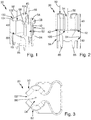
- the Figs. 1 to 4 show various views of a contact socket 20 according to the invention.
- the contact socket 20 is designed for electrical connection with a plug 200. It is a one-piece stamped and bent part made of sheet metal that is electrically conductive.
- the contact socket 20 is preferably a maximum of 20 mm high, a maximum of 10 mm wide and a maximum of 10 mm deep.
- the contact socket 20 has a plug receiving section 40 and a support section 80.
- the support section 80 is arranged opposite the plug receiving section 40.
- the plug receiving section 40 has a first clamping leg 50 and a second clamping leg 60 opposite this. Between the two clamping legs 50, 60 there is a separating slot 52 which separates them from one another and a touching contact prevented between them.
- the two clamping legs 50, 60 delimit a connector receiving space 54 into which the connector 200 can be inserted or pushed.
- the connector receiving space 54 is rectangular, see Fig. 3 , and has a longitudinal axis 56.
- the connector receiving space 54 is arranged within the connector receiving section 40.
- the contact socket 20 has a rear wall 100 which is arranged parallel and offset to the longitudinal axis 56 and within the plug receiving section 40 and the support section 80.
- the rear wall 100 is delimited at a free end of the contact socket 20 by an outer edge 102.
- the rear wall is laterally bounded by two edges 104, on which a first spring section 45 and a second spring section 55 are arranged within the plug receiving section 40.
- the first clamping leg 50 is arranged on the first spring section 45 and the second clamping leg 60 is arranged on the second spring section 55.
- the two spring sections 45, 55 are designed to elastically enlarge the connector receiving space 54 due to the resilience of the clamping legs 50 and 60.
- the two clamping legs 50, 60 each have at the upper end a first insertion bevel 58 and a second insertion bevel 68, which face the connector receiving space 54.
- a respective lead-in bevel 58, 68 is bent outward in the radial direction in such a way that the two lead-in bevels 58, 68 enlarge the connector receiving space 54 in the radial direction.
- the insertion bevels 58, 68 preferably enlarge the plug receiving space 54 such that a diameter of a cross section transverse to the longitudinal axis 56 through the insertion bevel 58, 68 is greater than a diameter of the plug 200. It can thus be easily inserted.
- both insertion bevels 58, 68 interact in a manner known per se with the plug 200 in such a way that the plug receiving space 54 is elastically enlarged.
- the plug 200 is inserted into the plug receiving space 54, it is pushed towards the support section 80 in the direction of the longitudinal axis 56.
- the plug 200 first strikes against one of the two lead-in bevels 58, 68 and slides along this lead-in bevel 58, 68 until the plug 200 strikes both lead-in bevels 58, 68.
- the plug 200 If the plug 200 is pushed further towards the support section 80, it presses the two clamping legs 50, 60 apart, as a result of which the plug receiving space 54 is elastically enlarged and the two spring sections 45, 55 are pretensioned.
- the plug receiving space 54 is enlarged by the plug 200 in such a way that it can be inserted or plugged into the plug receiving space 54 as intended.
- the plug 200 is clamped between the two clamping legs 50, 60 and is held by them.
- FIG Fig. 4 A plug 200 inserted into the plug receiving space 54 is shown in FIG Fig. 4 shown.
- the plug 200 is a one-piece stamped and bent part made of suitable sheet metal that is electrically conductive.
- the plug 200 has a cylindrical plug section 205 which is clamped or held between the two clamping legs 50, 60.
- the two clamping legs 50, 60 contact the connector section 205 mainly at four line contacts 62.
- the connector pull-off force should be selected in such a way that the clamping between the clamping legs 50, 60 and the connector 200 can be overcome. If the plug 200 is no longer received by the plug receiving space 54, the preload of the two spring sections 45, 55 is released, and the two clamping legs 50, 60 are moved towards each other by releasing the preload, the plug receiving space 54 being reduced in size.
- Fig. 2 shows that the rear wall 100 has a connecting section 106, within which the plug receiving section 40 is connected to the support section 80.
- the support section 80 is connected to the plug receiving section 40 via the rear wall 100.
- Two slots 42 partially separate the plug receiving section 40 from the support section 80 from one another.
- the support section 80 is roughly cuboid.
- Figs. 1 and 2 show that a force 82 acts parallel to the longitudinal axis 56 on the plug receiving section 40, in particular on the second spring section 55, and acts in the direction of the support section 80.
- This force 82 can typically occur during the intended use of the contact socket 20, in particular when a plug holder with the plug is inserted into the plug receiving space 54 by a fitter. This can happen above all if, instead of inserting the plug into the plug receiving space, the user presses with the plug holder or the plug on the rear wall 100 and / or on one of the two spring sections 45, 55.
- the rear wall 100 is bent and pretensioned with the narrowing of the slot 42 until one of the two spring sections 45, 55 touches one of two side walls 84 of the support section 80 and is supported on it.
- the latter at least partially absorbs the force 82.
- the plug receiving section 40 is supported by the support section 80 when the force 82 acts on the plug receiving section 40 in the direction of the longitudinal axis 56 and in the direction of the support section 80.
- the force 82 no longer acts on the plug receiving section 40, the Pre-tensioning of the rear wall 100, and the rear wall 100 is moved into its original position as a result of this release of the pre-tension with the expansion of the slot 42.
- the support section 80 has a number of fastening elements 86 in the form of protruding pins as retaining legs, which are designed for through-mounting the contact socket 20 on a printed circuit board.
- Figs. 1 and 2 show that the contact socket 20 has a total of six such fastening elements 86.
- the contact socket can also have a different number, for example four, eight, ten, twelve fastening elements 86. These fastening elements 86 are inserted through openings in the circuit board and then connected to the circuit board by soldering to contact fields on the underside.
- the fastening elements 86 are preferably designed to fasten the contact socket 20 on the printed circuit board and at the same time to electrically connect the contact socket 20 to the printed circuit board as described above when the contact socket 20 is fastened to the printed circuit board. If the contact socket 20 is attached to the circuit board and the force 82 acts and the plug receiving section 40 is supported by the support section 80, then the circuit board can at least partially absorb the force 82.
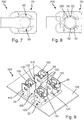
- Figures 5 to 8 show various views of an alternative embodiment 20 'of the contact socket from FIG Figs. 1 to 4 .
- the same reference numerals are used for identical and functionally equivalent elements and in this respect the above statements on the Figs. 1 to 4 to get expelled. Essentially, only the existing differences are discussed below.
- the connector receiving section 40 and the support section 80 are each rectangular in cross section perpendicular to the longitudinal axis 56.
- Contact socket 20 ′ shown has a first side wall 110 and a second side wall 120, which are arranged within the plug receiving section 40 and the support section 80.
- Both side walls 110, 120 are each arranged on an edge 104 running perpendicular to the outer edge 102 of the rear wall 100.
- Both side walls 110, 120 are parallel to the longitudinal axis 56 of the connector receiving space 54 and orthogonal to the rear wall 100.
- the first side wall 110 and the second side wall 120 are parallel to one another.
- the rear wall 100 and the two side walls 110, 120 delimit the plug receiving section 40 and the support section 80.
- the first side wall 110 has a first side wall outer edge 112 and the second side wall 120 has a second side wall outer edge 122.
- the first spring section 45 and the first spring section 45 are each on an edge 114, 124 running towards the side wall outer edge 112, 122 second spring portion 55 arranged.
- the first spring section 45 and the second spring section 55 delimit the plug receiving section 40.
- the outer edge 102 of the rear wall 100 and the two side wall outer edges 112, 122 delimit the contact socket 20 'at the free end and lie within a plane.
- Fig. 5 shows that the outer edge 102 of the rear wall 100 and the two side wall outer edges 112, 122 protrude beyond the two lead-in bevels 58, 68 in the direction of the longitudinal axis 56.
- the two clamping legs 50, 60 in particular the two lead-in bevels 58, 68, do not protrude beyond the rear wall 100 and beyond the two side walls 110, 120.
- the two clamping legs 58, 68 are protected from inadvertent contact with the connector holder, especially if it is used incorrectly.
- Fig. 6 shows that the two side walls 110, 120 each have a latching element 116, 126 in the form of an opening, which is designed to interact with corresponding latching elements in the form of latching lugs of the connector holder, the latching lugs snap into the openings when the plug 200 is in the connector receiving space 54 is inserted.
- the latching elements secure the plug 200 in the plug receiving space 54 against unintentional removal of the plug 200 from the plug receiving space 54.
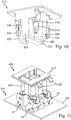
- Fig. 9 shows a circuit board arrangement 300 with a circuit board 150 on which a first contact socket 21, a second contact socket 22, a third contact socket 23 and a fourth contact socket 24 are attached and electrically connected to the circuit board 150.
- All four contact sockets 21, 22, 23, 24 are identical in structure and agree with the previously described contact socket 20 'of the Figures 5 to 8 match.
- the same reference symbols are used for identical and functionally equivalent elements. In this respect, reference is made to the above statements on Figures 1 to 8 , in particular Figures 5 to 8 , so that essentially only the existing differences will be discussed below.
- the four contact sockets 21, 22, 23, 24 are arranged on the circuit board 150 in such a way that the rear wall 100 of the first contact socket 21 is parallel and offset to the rear wall 100 of the second contact socket 22.
- the first side wall 110 of the first contact socket 21 is parallel and offset to the first side wall 110 of the third contact socket 23.
- the first side wall 110 of the first contact socket 21 and the second side wall 120 of the second contact socket 22 arranged within a plane.
- the rear wall 100 of the first contact socket 21 and the rear wall 100 of the second contact socket 22 face one another and are spaced apart from one another. There is a gap 160 between the two rear walls 100 of the first contact socket 21 and the second contact socket 22.
- the rear wall 100 of the first contact socket 21 and the rear wall 100 of the third contact socket 23 are also arranged within one plane.
- the second side wall 120 of the first female contact 100 and the first side wall 110 of the third female contact 23 face one another and are spaced apart from one another.
- the rear wall 100 of the second contact socket 22 and the rear wall 100 of the fourth contact socket 24 are also arranged within one plane.
- the first side wall 110 of the second female contact 22 and the second side wall 120 of the fourth female contact 24 face one another and are spaced apart from one another.
- the gap 160 between the rear walls 100 of the third contact socket 23 and the fourth contact socket 24 and the gap 162 between the first side wall 110 and the second side wall 120 continue.
- the gap 160 and the gap 162 together result in a cruciform shape which runs between all four contact sockets 21, 22, 23, 24.
- the two gaps 160, 162 are designed to receive a centering projection of the connector holder.
- Fig. 10 shows a connector holder 210.
- This connector holder 210 has four retaining pegs 215 which are designed to receive four identical hollow cylindrical connectors 200, the connectors 200 being preferably connected to the retaining pegs 215 via a press fit.
- Each of the holding pegs 215 has a latching lug 216 which engages in a corresponding latching recess in the plug 200 when the plug 200 is pressed onto the holding peg 215.
- the hollow cylindrical plug 200 it would also be possible to use the usual solid or closed plugs.
- the connector holder 210 also has a centering projection 220 which is designed to be inserted into the two columns 160, 162 of the FIG Fig. 9 shown arrangement of contact sockets 21, 22, 23, 24 to be arranged or inserted.
- the centering projection 220 has four protruding wall sections 222, 224, 226, 228, the number of which corresponds to that of the contact sockets 21, 22, 23, 24 of the circuit board arrangement Fig. 9 corresponds to. All four protruding wall sections 222, 224, 226, 228 protrude in different directions.
- the centering projection 220 has a free end on which a centering bevel 225 is arranged. This centering bevel 225 runs around the centering projection 220.
- the centering projection 220 is designed to press against the side walls 110, 120 and / or the rear walls 100 of the in Fig. 9 contact sockets 21, 22, 23, 24 shown when the plug holder 210 with plugs 200 is to be inserted into the plug receiving spaces 54.
- the centering bevel 225 slides on the abutted side wall 110, 120 and / or rear wall 100 until the centering projection 220 has largely aligned the plugs 200 relative to the plug receiving spaces 54 in such a way that they can be easily and completely correctly inserted into the plug receiving spaces 54 of the contact sockets 21, 22, 23, 24 can.
- the centering bevel 225 therefore aligns the plug 200 relative to the plug receiving spaces 54 in such a way that they are aligned concentrically with the plug receiving spaces 54 and can be inserted into them.
- Fig. 11 shows a connector system 400 with the circuit board arrangement from Fig. 9 and the connector holder 210 Fig. 10 .
- a plug 200 is arranged on each of the retaining pins 215.
- a pulled-out state of the plug-in system 400 is shown, the plug holder 210 with the plugs 200 already being positioned in such a way that it only needs to be pressed towards the circuit board 150 in the direction of the longitudinal axis 56 in order to achieve an inserted state.
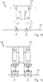
- Figures 12 and 13 show the connector system 400 Fig. 11 from two different side views.
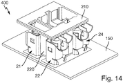
- Fig. 14 shows the connector system 400 in an inserted state in which the connectors 200 are arranged in the respective corresponding connector receiving spaces 64 of the circuit board arrangement 300.
- the centering projection 220 is also arranged between the rear walls 100 of the contact sockets 21, 22, 23, 24.
- the centering projection 220 is also arranged between the first side wall 110 and the second side wall 120.
- the centering projection 220 is arranged between the first side wall 110 of the third contact socket 23 and the second side wall 120 of the first contact socket 21.
- the centering projection 220 advantageously insulates the individual contact sockets 21, 22, 23, 24 electrically from one another in the direction of a direct connection between the individual contact sockets 21, 22, 23, 24.
Landscapes
- Coupling Device And Connection With Printed Circuit (AREA)
Applications Claiming Priority (1)
| Application Number | Priority Date | Filing Date | Title |
|---|---|---|---|
| DE102019214012.2A DE102019214012A1 (de) | 2019-09-13 | 2019-09-13 | Kontaktbuchse, Leiterplattenanordnung und Stecksystem damit |
Publications (2)
| Publication Number | Publication Date |
|---|---|
| EP3793036A1 true EP3793036A1 (fr) | 2021-03-17 |
| EP3793036B1 EP3793036B1 (fr) | 2022-11-23 |
Family
ID=72340227
Family Applications (1)
| Application Number | Title | Priority Date | Filing Date |
|---|---|---|---|
| EP20194014.5A Active EP3793036B1 (fr) | 2019-09-13 | 2020-09-02 | Prise de contact, dispositif de carte de circuit imprimé et système enfichable correspondant |
Country Status (3)
| Country | Link |
|---|---|
| EP (1) | EP3793036B1 (fr) |
| DE (1) | DE102019214012A1 (fr) |
| ES (1) | ES2939006T3 (fr) |
Cited By (2)
| Publication number | Priority date | Publication date | Assignee | Title |
|---|---|---|---|---|
| CN114696138A (zh) * | 2022-04-11 | 2022-07-01 | 宁波公牛电器有限公司 | 一种插座 |
| CN115995722A (zh) * | 2021-10-18 | 2023-04-21 | 明泰科技股份有限公司 | 浮动电连接器及电路连接构造 |
Families Citing this family (1)
| Publication number | Priority date | Publication date | Assignee | Title |
|---|---|---|---|---|
| EP4518036A1 (fr) * | 2023-06-06 | 2025-03-05 | Delphi Technologies IP Limited | Borne de montage sur circuit imprimé pour applications à courant élevé |
Citations (8)
| Publication number | Priority date | Publication date | Assignee | Title |
|---|---|---|---|---|
| GB418244A (en) * | 1933-06-21 | 1934-10-22 | A P Lundberg And Sons Ltd | Improvements in or relating to a combined spring-clip contact and terminal for electrical apparatus |
| DE7638508U1 (de) * | 1976-12-09 | 1977-04-28 | Grote & Hartmann Gmbh & Co Kg, 5600 Wuppertal | Steckfeder fuer gedruckte schaltungen |
| EP0110084A1 (fr) * | 1982-11-26 | 1984-06-13 | Robert Bosch Gmbh | Elément de distribution électrique |
| EP0908966A1 (fr) * | 1997-10-06 | 1999-04-14 | Legrand | Bloc de contact pour socle de prise de courant |
| CH693727A5 (de) * | 1998-08-25 | 2003-12-31 | Feller Ag | Kontaktfeder sowie Steckdose mit derselben. |
| DE102007063592A1 (de) * | 2007-12-21 | 2009-07-02 | Merten Gmbh & Co. Kg | Kontaktelement |
| EP3104665A1 (fr) | 2015-06-10 | 2016-12-14 | E.G.O. ELEKTRO-GERÄTEBAU GmbH | Dispositif de chauffage a induction et champ de cuisson a induction equipe d'un tel dispositif de chauffage a induction |
| EP3611804A1 (fr) * | 2018-08-13 | 2020-02-19 | Valeo Siemens eAutomotive France SAS | Equipement electrique |
Family Cites Families (1)
| Publication number | Priority date | Publication date | Assignee | Title |
|---|---|---|---|---|
| JP5501143B2 (ja) * | 2010-07-30 | 2014-05-21 | タイコエレクトロニクスジャパン合同会社 | コンタクトおよび電気コネクタ |
-
2019
- 2019-09-13 DE DE102019214012.2A patent/DE102019214012A1/de not_active Withdrawn
-
2020
- 2020-09-02 ES ES20194014T patent/ES2939006T3/es active Active
- 2020-09-02 EP EP20194014.5A patent/EP3793036B1/fr active Active
Patent Citations (8)
| Publication number | Priority date | Publication date | Assignee | Title |
|---|---|---|---|---|
| GB418244A (en) * | 1933-06-21 | 1934-10-22 | A P Lundberg And Sons Ltd | Improvements in or relating to a combined spring-clip contact and terminal for electrical apparatus |
| DE7638508U1 (de) * | 1976-12-09 | 1977-04-28 | Grote & Hartmann Gmbh & Co Kg, 5600 Wuppertal | Steckfeder fuer gedruckte schaltungen |
| EP0110084A1 (fr) * | 1982-11-26 | 1984-06-13 | Robert Bosch Gmbh | Elément de distribution électrique |
| EP0908966A1 (fr) * | 1997-10-06 | 1999-04-14 | Legrand | Bloc de contact pour socle de prise de courant |
| CH693727A5 (de) * | 1998-08-25 | 2003-12-31 | Feller Ag | Kontaktfeder sowie Steckdose mit derselben. |
| DE102007063592A1 (de) * | 2007-12-21 | 2009-07-02 | Merten Gmbh & Co. Kg | Kontaktelement |
| EP3104665A1 (fr) | 2015-06-10 | 2016-12-14 | E.G.O. ELEKTRO-GERÄTEBAU GmbH | Dispositif de chauffage a induction et champ de cuisson a induction equipe d'un tel dispositif de chauffage a induction |
| EP3611804A1 (fr) * | 2018-08-13 | 2020-02-19 | Valeo Siemens eAutomotive France SAS | Equipement electrique |
Cited By (2)
| Publication number | Priority date | Publication date | Assignee | Title |
|---|---|---|---|---|
| CN115995722A (zh) * | 2021-10-18 | 2023-04-21 | 明泰科技股份有限公司 | 浮动电连接器及电路连接构造 |
| CN114696138A (zh) * | 2022-04-11 | 2022-07-01 | 宁波公牛电器有限公司 | 一种插座 |
Also Published As
| Publication number | Publication date |
|---|---|
| ES2939006T3 (es) | 2023-04-18 |
| EP3793036B1 (fr) | 2022-11-23 |
| DE102019214012A1 (de) | 2021-03-18 |
Similar Documents
| Publication | Publication Date | Title |
|---|---|---|
| DE2406125C3 (de) | Buchsenkontakt | |
| DE102013111649B4 (de) | Einzelelement-Draht/Platte-Verbinder | |
| EP1657789B1 (fr) | Dispositif de connexion pour connexion directe de la partie finale de conducteurs et appareil avec un tel dispositif de connexion | |
| DE102015211002B4 (de) | Verbinder mit einem Verbindergehäuse und einem Verbinderanschluss | |
| DE29920231U1 (de) | Schraubenlose Anschlußklemme | |
| DE3234095A1 (de) | Montagesockel fuer elektronische bauteile | |
| DE3934790C2 (de) | Elektrische Steckverbindung | |
| DE2941029A1 (de) | Zum einpressverbinden mit einem elektrischen leiter vorgesehenen elektrischen anschlussteil, verfahren zum verbinden eines anschlussteils mit einem elektrischen leiter sowie verbinder mit einer mehrzahl elektrischer anschlussteile | |
| DE102014108965A1 (de) | Einzelelement-Verbinder Draht zu Platte | |
| EP3793036B1 (fr) | Prise de contact, dispositif de carte de circuit imprimé et système enfichable correspondant | |
| EP3782235B1 (fr) | Connecteur direct | |
| DE602005000836T2 (de) | Elektrischer Steckverbinder | |
| DE2546189C3 (de) | In einem Schalungsträger einsetzbare Kontaktbuchse | |
| DE3810209C2 (fr) | ||
| DE102015211725B4 (de) | Verbinderanschluss und Verbinder hiermit | |
| DE69328387T2 (de) | Leiterplatte mit stützender Randverbinder-Einrichtung, Verfahren für deren Zusammenbau sowie Verbinder zu deren Aufnahme | |
| DE3781997T2 (de) | Geschlitzte anschlusseinrichtung fuer elektrisches kabel und dementsprechendes anschlusswerkzeug. | |
| DE2536184A1 (de) | Kontaktelement | |
| EP0483532B1 (fr) | Dispositifs de connexion pour circuits imprimés | |
| EP1154521B1 (fr) | Connecteur et procédé de montage de connecteur | |
| EP3168933B1 (fr) | Borne de prise électrique | |
| DE20113884U1 (de) | Elektrischer Verbinder für eine Leiterplatte | |
| EP3201994A1 (fr) | Barrette à broches | |
| DE8010402U1 (de) | Halter für elektrotechnische Bauteile mit stirnseitigen Kontaktflächen | |
| DE102019122328A1 (de) | Elektrischer Steckverbinder und Steckverbinderanordnung |
Legal Events
| Date | Code | Title | Description |
|---|---|---|---|
| PUAI | Public reference made under article 153(3) epc to a published international application that has entered the european phase |
Free format text: ORIGINAL CODE: 0009012 |
|
| STAA | Information on the status of an ep patent application or granted ep patent |
Free format text: STATUS: THE APPLICATION HAS BEEN PUBLISHED |
|
| AK | Designated contracting states |
Kind code of ref document: A1 Designated state(s): AL AT BE BG CH CY CZ DE DK EE ES FI FR GB GR HR HU IE IS IT LI LT LU LV MC MK MT NL NO PL PT RO RS SE SI SK SM TR |
|
| AX | Request for extension of the european patent |
Extension state: BA ME |
|
| STAA | Information on the status of an ep patent application or granted ep patent |
Free format text: STATUS: REQUEST FOR EXAMINATION WAS MADE |
|
| 17P | Request for examination filed |
Effective date: 20210830 |
|
| RBV | Designated contracting states (corrected) |
Designated state(s): AL AT BE BG CH CY CZ DE DK EE ES FI FR GB GR HR HU IE IS IT LI LT LU LV MC MK MT NL NO PL PT RO RS SE SI SK SM TR |
|
| GRAP | Despatch of communication of intention to grant a patent |
Free format text: ORIGINAL CODE: EPIDOSNIGR1 |
|
| STAA | Information on the status of an ep patent application or granted ep patent |
Free format text: STATUS: GRANT OF PATENT IS INTENDED |
|
| INTG | Intention to grant announced |
Effective date: 20220712 |
|
| GRAS | Grant fee paid |
Free format text: ORIGINAL CODE: EPIDOSNIGR3 |
|
| GRAA | (expected) grant |
Free format text: ORIGINAL CODE: 0009210 |
|
| STAA | Information on the status of an ep patent application or granted ep patent |
Free format text: STATUS: THE PATENT HAS BEEN GRANTED |
|
| AK | Designated contracting states |
Kind code of ref document: B1 Designated state(s): AL AT BE BG CH CY CZ DE DK EE ES FI FR GB GR HR HU IE IS IT LI LT LU LV MC MK MT NL NO PL PT RO RS SE SI SK SM TR |
|
| REG | Reference to a national code |
Ref country code: GB Ref legal event code: FG4D Free format text: NOT ENGLISH |
|
| REG | Reference to a national code |
Ref country code: CH Ref legal event code: EP |
|
| REG | Reference to a national code |
Ref country code: DE Ref legal event code: R096 Ref document number: 502020002044 Country of ref document: DE |
|
| REG | Reference to a national code |
Ref country code: AT Ref legal event code: REF Ref document number: 1533725 Country of ref document: AT Kind code of ref document: T Effective date: 20221215 |
|
| REG | Reference to a national code |
Ref country code: IE Ref legal event code: FG4D Free format text: LANGUAGE OF EP DOCUMENT: GERMAN |
|
| REG | Reference to a national code |
Ref country code: LT Ref legal event code: MG9D |
|
| REG | Reference to a national code |
Ref country code: NL Ref legal event code: MP Effective date: 20221123 |
|
| REG | Reference to a national code |
Ref country code: ES Ref legal event code: FG2A Ref document number: 2939006 Country of ref document: ES Kind code of ref document: T3 Effective date: 20230418 |
|
| PG25 | Lapsed in a contracting state [announced via postgrant information from national office to epo] |
Ref country code: SE Free format text: LAPSE BECAUSE OF FAILURE TO SUBMIT A TRANSLATION OF THE DESCRIPTION OR TO PAY THE FEE WITHIN THE PRESCRIBED TIME-LIMIT Effective date: 20221123 Ref country code: PT Free format text: LAPSE BECAUSE OF FAILURE TO SUBMIT A TRANSLATION OF THE DESCRIPTION OR TO PAY THE FEE WITHIN THE PRESCRIBED TIME-LIMIT Effective date: 20230323 Ref country code: NO Free format text: LAPSE BECAUSE OF FAILURE TO SUBMIT A TRANSLATION OF THE DESCRIPTION OR TO PAY THE FEE WITHIN THE PRESCRIBED TIME-LIMIT Effective date: 20230223 Ref country code: LT Free format text: LAPSE BECAUSE OF FAILURE TO SUBMIT A TRANSLATION OF THE DESCRIPTION OR TO PAY THE FEE WITHIN THE PRESCRIBED TIME-LIMIT Effective date: 20221123 Ref country code: FI Free format text: LAPSE BECAUSE OF FAILURE TO SUBMIT A TRANSLATION OF THE DESCRIPTION OR TO PAY THE FEE WITHIN THE PRESCRIBED TIME-LIMIT Effective date: 20221123 |
|
| PG25 | Lapsed in a contracting state [announced via postgrant information from national office to epo] |
Ref country code: RS Free format text: LAPSE BECAUSE OF FAILURE TO SUBMIT A TRANSLATION OF THE DESCRIPTION OR TO PAY THE FEE WITHIN THE PRESCRIBED TIME-LIMIT Effective date: 20221123 Ref country code: PL Free format text: LAPSE BECAUSE OF FAILURE TO SUBMIT A TRANSLATION OF THE DESCRIPTION OR TO PAY THE FEE WITHIN THE PRESCRIBED TIME-LIMIT Effective date: 20221123 Ref country code: LV Free format text: LAPSE BECAUSE OF FAILURE TO SUBMIT A TRANSLATION OF THE DESCRIPTION OR TO PAY THE FEE WITHIN THE PRESCRIBED TIME-LIMIT Effective date: 20221123 Ref country code: IS Free format text: LAPSE BECAUSE OF FAILURE TO SUBMIT A TRANSLATION OF THE DESCRIPTION OR TO PAY THE FEE WITHIN THE PRESCRIBED TIME-LIMIT Effective date: 20230323 Ref country code: HR Free format text: LAPSE BECAUSE OF FAILURE TO SUBMIT A TRANSLATION OF THE DESCRIPTION OR TO PAY THE FEE WITHIN THE PRESCRIBED TIME-LIMIT Effective date: 20221123 Ref country code: GR Free format text: LAPSE BECAUSE OF FAILURE TO SUBMIT A TRANSLATION OF THE DESCRIPTION OR TO PAY THE FEE WITHIN THE PRESCRIBED TIME-LIMIT Effective date: 20230224 |
|
| PG25 | Lapsed in a contracting state [announced via postgrant information from national office to epo] |
Ref country code: NL Free format text: LAPSE BECAUSE OF FAILURE TO SUBMIT A TRANSLATION OF THE DESCRIPTION OR TO PAY THE FEE WITHIN THE PRESCRIBED TIME-LIMIT Effective date: 20221123 |
|
| PG25 | Lapsed in a contracting state [announced via postgrant information from national office to epo] |
Ref country code: SM Free format text: LAPSE BECAUSE OF FAILURE TO SUBMIT A TRANSLATION OF THE DESCRIPTION OR TO PAY THE FEE WITHIN THE PRESCRIBED TIME-LIMIT Effective date: 20221123 Ref country code: RO Free format text: LAPSE BECAUSE OF FAILURE TO SUBMIT A TRANSLATION OF THE DESCRIPTION OR TO PAY THE FEE WITHIN THE PRESCRIBED TIME-LIMIT Effective date: 20221123 Ref country code: EE Free format text: LAPSE BECAUSE OF FAILURE TO SUBMIT A TRANSLATION OF THE DESCRIPTION OR TO PAY THE FEE WITHIN THE PRESCRIBED TIME-LIMIT Effective date: 20221123 Ref country code: DK Free format text: LAPSE BECAUSE OF FAILURE TO SUBMIT A TRANSLATION OF THE DESCRIPTION OR TO PAY THE FEE WITHIN THE PRESCRIBED TIME-LIMIT Effective date: 20221123 Ref country code: CZ Free format text: LAPSE BECAUSE OF FAILURE TO SUBMIT A TRANSLATION OF THE DESCRIPTION OR TO PAY THE FEE WITHIN THE PRESCRIBED TIME-LIMIT Effective date: 20221123 |
|
| REG | Reference to a national code |
Ref country code: DE Ref legal event code: R097 Ref document number: 502020002044 Country of ref document: DE |
|
| PG25 | Lapsed in a contracting state [announced via postgrant information from national office to epo] |
Ref country code: SK Free format text: LAPSE BECAUSE OF FAILURE TO SUBMIT A TRANSLATION OF THE DESCRIPTION OR TO PAY THE FEE WITHIN THE PRESCRIBED TIME-LIMIT Effective date: 20221123 Ref country code: AL Free format text: LAPSE BECAUSE OF FAILURE TO SUBMIT A TRANSLATION OF THE DESCRIPTION OR TO PAY THE FEE WITHIN THE PRESCRIBED TIME-LIMIT Effective date: 20221123 |
|
| PLBE | No opposition filed within time limit |
Free format text: ORIGINAL CODE: 0009261 |
|
| STAA | Information on the status of an ep patent application or granted ep patent |
Free format text: STATUS: NO OPPOSITION FILED WITHIN TIME LIMIT |
|
| 26N | No opposition filed |
Effective date: 20230824 |
|
| PG25 | Lapsed in a contracting state [announced via postgrant information from national office to epo] |
Ref country code: SI Free format text: LAPSE BECAUSE OF FAILURE TO SUBMIT A TRANSLATION OF THE DESCRIPTION OR TO PAY THE FEE WITHIN THE PRESCRIBED TIME-LIMIT Effective date: 20221123 |
|
| REG | Reference to a national code |
Ref country code: CH Ref legal event code: PL |
|
| PG25 | Lapsed in a contracting state [announced via postgrant information from national office to epo] |
Ref country code: LU Free format text: LAPSE BECAUSE OF NON-PAYMENT OF DUE FEES Effective date: 20230902 |
|
| REG | Reference to a national code |
Ref country code: BE Ref legal event code: MM Effective date: 20230930 |
|
| PG25 | Lapsed in a contracting state [announced via postgrant information from national office to epo] |
Ref country code: LU Free format text: LAPSE BECAUSE OF NON-PAYMENT OF DUE FEES Effective date: 20230902 Ref country code: MC Free format text: LAPSE BECAUSE OF FAILURE TO SUBMIT A TRANSLATION OF THE DESCRIPTION OR TO PAY THE FEE WITHIN THE PRESCRIBED TIME-LIMIT Effective date: 20221123 |
|
| REG | Reference to a national code |
Ref country code: IE Ref legal event code: MM4A |
|
| PG25 | Lapsed in a contracting state [announced via postgrant information from national office to epo] |
Ref country code: IE Free format text: LAPSE BECAUSE OF NON-PAYMENT OF DUE FEES Effective date: 20230902 |
|
| PG25 | Lapsed in a contracting state [announced via postgrant information from national office to epo] |
Ref country code: CH Free format text: LAPSE BECAUSE OF NON-PAYMENT OF DUE FEES Effective date: 20230930 |
|
| PG25 | Lapsed in a contracting state [announced via postgrant information from national office to epo] |
Ref country code: IE Free format text: LAPSE BECAUSE OF NON-PAYMENT OF DUE FEES Effective date: 20230902 Ref country code: CH Free format text: LAPSE BECAUSE OF NON-PAYMENT OF DUE FEES Effective date: 20230930 |
|
| PG25 | Lapsed in a contracting state [announced via postgrant information from national office to epo] |
Ref country code: BE Free format text: LAPSE BECAUSE OF NON-PAYMENT OF DUE FEES Effective date: 20230930 |
|
| PG25 | Lapsed in a contracting state [announced via postgrant information from national office to epo] |
Ref country code: BG Free format text: LAPSE BECAUSE OF FAILURE TO SUBMIT A TRANSLATION OF THE DESCRIPTION OR TO PAY THE FEE WITHIN THE PRESCRIBED TIME-LIMIT Effective date: 20221123 |
|
| PG25 | Lapsed in a contracting state [announced via postgrant information from national office to epo] |
Ref country code: BG Free format text: LAPSE BECAUSE OF FAILURE TO SUBMIT A TRANSLATION OF THE DESCRIPTION OR TO PAY THE FEE WITHIN THE PRESCRIBED TIME-LIMIT Effective date: 20221123 |
|
| GBPC | Gb: european patent ceased through non-payment of renewal fee |
Effective date: 20240902 |
|
| PG25 | Lapsed in a contracting state [announced via postgrant information from national office to epo] |
Ref country code: GB Free format text: LAPSE BECAUSE OF NON-PAYMENT OF DUE FEES Effective date: 20240902 |
|
| PG25 | Lapsed in a contracting state [announced via postgrant information from national office to epo] |
Ref country code: CY Free format text: LAPSE BECAUSE OF FAILURE TO SUBMIT A TRANSLATION OF THE DESCRIPTION OR TO PAY THE FEE WITHIN THE PRESCRIBED TIME-LIMIT; INVALID AB INITIO Effective date: 20200902 |
|
| PG25 | Lapsed in a contracting state [announced via postgrant information from national office to epo] |
Ref country code: HU Free format text: LAPSE BECAUSE OF FAILURE TO SUBMIT A TRANSLATION OF THE DESCRIPTION OR TO PAY THE FEE WITHIN THE PRESCRIBED TIME-LIMIT; INVALID AB INITIO Effective date: 20200902 |
|
| PGFP | Annual fee paid to national office [announced via postgrant information from national office to epo] |
Ref country code: DE Payment date: 20250919 Year of fee payment: 6 |
|
| PGFP | Annual fee paid to national office [announced via postgrant information from national office to epo] |
Ref country code: FR Payment date: 20250924 Year of fee payment: 6 Ref country code: AT Payment date: 20251020 Year of fee payment: 5 |
|
| PG25 | Lapsed in a contracting state [announced via postgrant information from national office to epo] |
Ref country code: TR Free format text: LAPSE BECAUSE OF FAILURE TO SUBMIT A TRANSLATION OF THE DESCRIPTION OR TO PAY THE FEE WITHIN THE PRESCRIBED TIME-LIMIT Effective date: 20221123 |
|
| PGFP | Annual fee paid to national office [announced via postgrant information from national office to epo] |
Ref country code: IT Payment date: 20250930 Year of fee payment: 6 |
|
| PGFP | Annual fee paid to national office [announced via postgrant information from national office to epo] |
Ref country code: ES Payment date: 20251020 Year of fee payment: 6 |