EP3796230B1 - Verfahren zur bestimmung von prozessgrenzen eines halbleiterprozesses - Google Patents
Verfahren zur bestimmung von prozessgrenzen eines halbleiterprozesses Download PDFInfo
- Publication number
- EP3796230B1 EP3796230B1 EP19197794.1A EP19197794A EP3796230B1 EP 3796230 B1 EP3796230 B1 EP 3796230B1 EP 19197794 A EP19197794 A EP 19197794A EP 3796230 B1 EP3796230 B1 EP 3796230B1
- Authority
- EP
- European Patent Office
- Prior art keywords
- images
- score
- query
- image
- dataset
- Prior art date
- Legal status (The legal status is an assumption and is not a legal conclusion. Google has not performed a legal analysis and makes no representation as to the accuracy of the status listed.)
- Active
Links
Images



Classifications
-
- G—PHYSICS
- G06—COMPUTING OR CALCULATING; COUNTING
- G06T—IMAGE DATA PROCESSING OR GENERATION, IN GENERAL
- G06T7/00—Image analysis
- G06T7/0002—Inspection of images, e.g. flaw detection
- G06T7/0004—Industrial image inspection
-
- G—PHYSICS
- G06—COMPUTING OR CALCULATING; COUNTING
- G06N—COMPUTING ARRANGEMENTS BASED ON SPECIFIC COMPUTATIONAL MODELS
- G06N3/00—Computing arrangements based on biological models
- G06N3/02—Neural networks
- G06N3/08—Learning methods
- G06N3/088—Non-supervised learning, e.g. competitive learning
-
- G—PHYSICS
- G03—PHOTOGRAPHY; CINEMATOGRAPHY; ANALOGOUS TECHNIQUES USING WAVES OTHER THAN OPTICAL WAVES; ELECTROGRAPHY; HOLOGRAPHY
- G03F—PHOTOMECHANICAL PRODUCTION OF TEXTURED OR PATTERNED SURFACES, e.g. FOR PRINTING, FOR PROCESSING OF SEMICONDUCTOR DEVICES; MATERIALS THEREFOR; ORIGINALS THEREFOR; APPARATUS SPECIALLY ADAPTED THEREFOR
- G03F7/00—Photomechanical, e.g. photolithographic, production of textured or patterned surfaces, e.g. printing surfaces; Materials therefor, e.g. comprising photoresists; Apparatus specially adapted therefor
- G03F7/70—Microphotolithographic exposure; Apparatus therefor
- G03F7/70483—Information management; Active and passive control; Testing; Wafer monitoring, e.g. pattern monitoring
- G03F7/70491—Information management, e.g. software; Active and passive control, e.g. details of controlling exposure processes or exposure tool monitoring processes
- G03F7/70508—Data handling in all parts of the microlithographic apparatus, e.g. handling pattern data for addressable masks or data transfer to or from different components within the exposure apparatus
-
- G—PHYSICS
- G03—PHOTOGRAPHY; CINEMATOGRAPHY; ANALOGOUS TECHNIQUES USING WAVES OTHER THAN OPTICAL WAVES; ELECTROGRAPHY; HOLOGRAPHY
- G03F—PHOTOMECHANICAL PRODUCTION OF TEXTURED OR PATTERNED SURFACES, e.g. FOR PRINTING, FOR PROCESSING OF SEMICONDUCTOR DEVICES; MATERIALS THEREFOR; ORIGINALS THEREFOR; APPARATUS SPECIALLY ADAPTED THEREFOR
- G03F7/00—Photomechanical, e.g. photolithographic, production of textured or patterned surfaces, e.g. printing surfaces; Materials therefor, e.g. comprising photoresists; Apparatus specially adapted therefor
- G03F7/70—Microphotolithographic exposure; Apparatus therefor
- G03F7/70483—Information management; Active and passive control; Testing; Wafer monitoring, e.g. pattern monitoring
- G03F7/70491—Information management, e.g. software; Active and passive control, e.g. details of controlling exposure processes or exposure tool monitoring processes
- G03F7/70525—Controlling normal operating mode, e.g. matching different apparatus, remote control or prediction of failure
-
- G—PHYSICS
- G03—PHOTOGRAPHY; CINEMATOGRAPHY; ANALOGOUS TECHNIQUES USING WAVES OTHER THAN OPTICAL WAVES; ELECTROGRAPHY; HOLOGRAPHY
- G03F—PHOTOMECHANICAL PRODUCTION OF TEXTURED OR PATTERNED SURFACES, e.g. FOR PRINTING, FOR PROCESSING OF SEMICONDUCTOR DEVICES; MATERIALS THEREFOR; ORIGINALS THEREFOR; APPARATUS SPECIALLY ADAPTED THEREFOR
- G03F7/00—Photomechanical, e.g. photolithographic, production of textured or patterned surfaces, e.g. printing surfaces; Materials therefor, e.g. comprising photoresists; Apparatus specially adapted therefor
- G03F7/70—Microphotolithographic exposure; Apparatus therefor
- G03F7/70483—Information management; Active and passive control; Testing; Wafer monitoring, e.g. pattern monitoring
- G03F7/70605—Workpiece metrology
- G03F7/70616—Monitoring the printed patterns
- G03F7/70625—Dimensions, e.g. line width, critical dimension [CD], profile, sidewall angle or edge roughness
-
- G—PHYSICS
- G03—PHOTOGRAPHY; CINEMATOGRAPHY; ANALOGOUS TECHNIQUES USING WAVES OTHER THAN OPTICAL WAVES; ELECTROGRAPHY; HOLOGRAPHY
- G03F—PHOTOMECHANICAL PRODUCTION OF TEXTURED OR PATTERNED SURFACES, e.g. FOR PRINTING, FOR PROCESSING OF SEMICONDUCTOR DEVICES; MATERIALS THEREFOR; ORIGINALS THEREFOR; APPARATUS SPECIALLY ADAPTED THEREFOR
- G03F7/00—Photomechanical, e.g. photolithographic, production of textured or patterned surfaces, e.g. printing surfaces; Materials therefor, e.g. comprising photoresists; Apparatus specially adapted therefor
- G03F7/70—Microphotolithographic exposure; Apparatus therefor
- G03F7/70483—Information management; Active and passive control; Testing; Wafer monitoring, e.g. pattern monitoring
- G03F7/70605—Workpiece metrology
- G03F7/70616—Monitoring the printed patterns
- G03F7/7065—Defects, e.g. optical inspection of patterned layer for defects
-
- G—PHYSICS
- G06—COMPUTING OR CALCULATING; COUNTING
- G06F—ELECTRIC DIGITAL DATA PROCESSING
- G06F16/00—Information retrieval; Database structures therefor; File system structures therefor
- G06F16/50—Information retrieval; Database structures therefor; File system structures therefor of still image data
- G06F16/53—Querying
-
- G—PHYSICS
- G06—COMPUTING OR CALCULATING; COUNTING
- G06F—ELECTRIC DIGITAL DATA PROCESSING
- G06F16/00—Information retrieval; Database structures therefor; File system structures therefor
- G06F16/50—Information retrieval; Database structures therefor; File system structures therefor of still image data
- G06F16/58—Retrieval characterised by using metadata, e.g. metadata not derived from the content or metadata generated manually
- G06F16/583—Retrieval characterised by using metadata, e.g. metadata not derived from the content or metadata generated manually using metadata automatically derived from the content
-
- G—PHYSICS
- G06—COMPUTING OR CALCULATING; COUNTING
- G06N—COMPUTING ARRANGEMENTS BASED ON SPECIFIC COMPUTATIONAL MODELS
- G06N20/00—Machine learning
-
- G—PHYSICS
- G06—COMPUTING OR CALCULATING; COUNTING
- G06N—COMPUTING ARRANGEMENTS BASED ON SPECIFIC COMPUTATIONAL MODELS
- G06N3/00—Computing arrangements based on biological models
- G06N3/02—Neural networks
- G06N3/04—Architecture, e.g. interconnection topology
- G06N3/045—Combinations of networks
-
- G—PHYSICS
- G06—COMPUTING OR CALCULATING; COUNTING
- G06N—COMPUTING ARRANGEMENTS BASED ON SPECIFIC COMPUTATIONAL MODELS
- G06N3/00—Computing arrangements based on biological models
- G06N3/02—Neural networks
- G06N3/04—Architecture, e.g. interconnection topology
- G06N3/045—Combinations of networks
- G06N3/0455—Auto-encoder networks; Encoder-decoder networks
-
- G—PHYSICS
- G06—COMPUTING OR CALCULATING; COUNTING
- G06N—COMPUTING ARRANGEMENTS BASED ON SPECIFIC COMPUTATIONAL MODELS
- G06N3/00—Computing arrangements based on biological models
- G06N3/02—Neural networks
- G06N3/04—Architecture, e.g. interconnection topology
- G06N3/047—Probabilistic or stochastic networks
-
- G—PHYSICS
- G06—COMPUTING OR CALCULATING; COUNTING
- G06N—COMPUTING ARRANGEMENTS BASED ON SPECIFIC COMPUTATIONAL MODELS
- G06N3/00—Computing arrangements based on biological models
- G06N3/02—Neural networks
- G06N3/04—Architecture, e.g. interconnection topology
- G06N3/0475—Generative networks
-
- G—PHYSICS
- G06—COMPUTING OR CALCULATING; COUNTING
- G06N—COMPUTING ARRANGEMENTS BASED ON SPECIFIC COMPUTATIONAL MODELS
- G06N3/00—Computing arrangements based on biological models
- G06N3/02—Neural networks
- G06N3/08—Learning methods
- G06N3/094—Adversarial learning
-
- G—PHYSICS
- G06—COMPUTING OR CALCULATING; COUNTING
- G06T—IMAGE DATA PROCESSING OR GENERATION, IN GENERAL
- G06T2207/00—Indexing scheme for image analysis or image enhancement
- G06T2207/10—Image acquisition modality
- G06T2207/10056—Microscopic image
- G06T2207/10061—Microscopic image from scanning electron microscope
-
- G—PHYSICS
- G06—COMPUTING OR CALCULATING; COUNTING
- G06T—IMAGE DATA PROCESSING OR GENERATION, IN GENERAL
- G06T2207/00—Indexing scheme for image analysis or image enhancement
- G06T2207/30—Subject of image; Context of image processing
- G06T2207/30108—Industrial image inspection
- G06T2207/30148—Semiconductor; IC; Wafer
Definitions
- a semiconductor device such as an integrated circuit chip is produced by a sequence of hundreds of process steps. Many of them require a lithographic mask through which a two-dimensional pattern is imprinted on a photoresist layer, followed by one or more etch processes for producing the pattern in the form of three-dimensional features formed in the material of a semiconductor wafer or of layers on the wafer.
- the design of such lithographic masks nowadays involves the prediction of the printed pattern taking into account optical, resist and etch phenomena, which occur at the scale of the mask features and below. These effects cause unavoidable deviations on the printed pattern with respect to the design intent.
- the printable window and the defect-related process window are examples of process limits needed for evaluating an OPC based mask design and/or for correctly printing a given set of features on a semiconductor wafer.
- Process limits are determined not only in terms of dose and focus applied in lithography processes, but also as a function of various other process parameters, such as etch parameters or parameters related to deposition or planarization processes. Today, the determination of these process limits equally requires a primarily manual analysis of CD-SEM images.
- the above described problems are related to the difficulty of distinguishing between different images of a die area obtained by a semiconductor process, wherein the different images are obtained by varying one or more process parameters.
- the different images are obtained by varying one or more process parameters.
- no reliable technique is available that allows to make this distinction without requiring extensive time and manual effort.
- the invention aims to provide a method for determining process limits that does not suffer from the above described problems. This aim is achieved by the method according to the appended claims.
- a dataset of detailed images of the same die area preferably CD-SEM images
- the images of the dataset correspond to different settings of one or more process parameters, for example different dose and focus settings applied in a lithographic process.
- One or more images from the dataset are used as training images of an unsupervised generative machine learning algorithm.
- the algorithm creates a latent vector space, comprising latent vectors that allow the algorithm to synthesize a large quantity of synthetic images.
- the method then presents one or more images from the dataset as query images to the algorithm, and a score is attributed to a set of object images from the dataset, based on the distances between the query image and respective object images, said distances being determined in the latent vector space.
- the score is representative of one or more characteristics of the images, such as the critical dimensions of one or more 2 or 3-dimensional features appearing in the images. This allows to extract the process limits directly from the score values, rather than from a manual comparison of the images.
- Obtaining a score value representative of a given image characteristic is enabled by a targeted choice of one or more of the query images and object images, and/or by determining the score as an aggregate score value, calculated from the scores obtained with respect to a set of different query images.
- the aggregate score may for example be the maximum or the average of the scores of the object images, obtained with respect to a set of query images.
- one or more synthetic images, generated by the algorithm are added to the dataset, and wherein one or more of said synthetic images are used as query images.
- the machine learning algorithm may be an algorithm of the type Generative Adversarial Network (GAN) or Variational Auto Encoder (Var-AE).
- GAN Generative Adversarial Network
- Var-AE Variational Auto Encoder
- the method may be used for determining a process window for one or more parameters of the process, wherein the process window determination is based on a predefined known relation between the scores and said one or more characteristics of the images.
- the predefined known relation may be based on one or more calibration steps performed prior to performing the method.
- the invention is equally related to an apparatus for determining process limits in accordance with the method of the invention, the apparatus comprising a computer configured to :
- the invention is equally related to a computer program product applicable in an apparatus according to the invention, and configured to
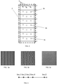
- the wafer portion 2 indicated in figure 1 is shown in an enlarged view in figure 2 , after printing the FEM wafer in a lithographic tool, at the various settings.
- Multiple pattern areas 3 on the die are examined, in order to determine the printable window in terms of the exposure and focus parameters, i.e. the ranges of exposure dose and focus within which the feature patterns as designed in these areas are effectively reproduced.
- CD-SEM images are taken of the areas in question.
- the printable window is linked to a step in the graph that sets out the CD as a function of dose and/or focus, i.e. a sudden rise or fall of the CD-curve.
- the present invention provides a way of automatically detecting the printable window.
- One or more of the CD-SEM images are used as training images for an unsupervised machine learning algorithm that creates a latent vector space on the basis of a pixel-by-pixel analysis of the training images. For example, if each of the images consist of an array of 256 by 256 pixels, each pixel may be attributed a value and a probability distribution, preferably a unit Gaussian.
- the algorithm transforms these data into a latent vector space through a neural network.
- the algorithm learns by a self-correcting sequence of image-synthesis and comparison to the training images, and thereby creates a large number of synthesized images, each image being defined by the values of its specific n-dimensional latent vector.
- this is done by selecting a single query image from the dataset, and comparing the query image to a set of other images from the dataset. These images will be referred to hereafter as 'object images'.
- the comparison is based on the distance in the latent vector space between the query image and the respective object images.
- the distance is the Euclidean distance between two n-dimensional latent vectors in the vector space.
- a score is attributed to the object images.
- the score is representative of the respective distances in the latent vector space, from the query image to the object images.
- the score may be the distance as such or any linear function of the distance. For example, the distance may be divided by a constant to obtain a normalized value of the distance, so that all scores are between 0 and 1.
- the maximum score is a suitable 'aggregate score' value, i.e. a score value based on the comparison of object images 1 to 5 to multiple query images, given that the outlier image 5 is in any case not related to a realistic CD.
- multiple images are used as query images, and at least one of the query images is an outlier image, i.e. an image for which it is known that it does not correspond to a CD value (or the value of another characteristic) within a predefined range of interest.
- the choice of the maximum score as the 'aggregate' score is one example of how the aggregate score is defined. Another possibility is taking the average of the scores of each column. Still other ways to define the aggregate score are included in the scope of the invention. What is needed is an aggregate score that behaves in a monotonic way for a sequence of images for which it is known that the CD (or another characteristic of the images) equally behaves monotonically in a given range of interest. If this is the case, the aggregate score will exhibit the same or very similar behaviour as the actual CD or other characteristic, as a function of dose and focus, and will therefore allow to extract a printable window.
- the score table as shown in tables 2 and 3 may be drawn up for the totality of the dataset, i.e. each of the 200 images is taken as the query image and each of the images is 'scored' as an object image relative to itself and to the other 199 images.
- the number of query images may however be smaller than the number of object images.
- the full set of 200 images may be 'scored' in relation to a smaller number, for example 50, query images.
- the dataset may be expanded by adding one or more synthetic images to it, for example a number of synthetic images for which it is known that they correspond to outlier images, and these synthetic images may be added to the list of query images in the first column of the table, and possibly also to the list of object images. This may help to obtain an aggregate score that corresponds well with the CD in the range of interest.
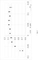
- Figure 6 shows an example of a score distribution obtained by the method of the invention, on the dies of a FEM wafer.
- Each number represents a score obtained in the above-described way, and wherein the query images, the object images and the definition of the aggregate score are chosen in such a way that the aggregate score behaves in the same way as the actual CD of a feature in the respective images.
- This is illustrated by the graph in Figure 7 , which shows normalized values of the CD and of the score relative to the same scale, as a function of the focus and for a dose setting of 41mJ/cm 2 , i.e. for the values of the column 10 highlighted in Figure 6 .
- the values of the CD and of the scores are normalized to the same dimensionless value.
- the scores furthermore closely follow the variations of the CD beyond the sharp rise.
- This result shows that it is possible to determine a CD-related process-window (i.e. a more narrow window within the limits of the printable window) on the basis of the score values alone, provided a preliminary calibration is performed.
- the calibration could entail the measurement of CDs on a limited number of images and the determination of a scale factor that allows to estimate the CD from the score values, possibly applying different scale factors in different ranges along the focus or dose axis, or determining a more intricate function that links the scores to the CD values. This allows to reconstruct the CDs from the scores, and to determine directly a CD-based process window from the score graph, without necessitating the manual inspection of a large number of CD-SEM images.
- the invention is therefore also related to such an apparatus and to a computer program product applicable in such an apparatus.
- the latter is a software product that includes the machine learning algorithm and that may further allow the user to perform a number of actions, such as the selection of training images, query images and object images, or the definition of the score.
- the software may also be configured to apply some of these actions automatically according to predefined selection and calculation criteria.
Landscapes
- Engineering & Computer Science (AREA)
- Physics & Mathematics (AREA)
- Theoretical Computer Science (AREA)
- General Physics & Mathematics (AREA)
- Data Mining & Analysis (AREA)
- General Engineering & Computer Science (AREA)
- Software Systems (AREA)
- Computing Systems (AREA)
- Artificial Intelligence (AREA)
- Mathematical Physics (AREA)
- Evolutionary Computation (AREA)
- Biophysics (AREA)
- General Health & Medical Sciences (AREA)
- Computational Linguistics (AREA)
- Biomedical Technology (AREA)
- Life Sciences & Earth Sciences (AREA)
- Health & Medical Sciences (AREA)
- Molecular Biology (AREA)
- Library & Information Science (AREA)
- Computer Vision & Pattern Recognition (AREA)
- Databases & Information Systems (AREA)
- Probability & Statistics with Applications (AREA)
- Quality & Reliability (AREA)
- Medical Informatics (AREA)
- Image Analysis (AREA)
Claims (14)
- Verfahren zum Bestimmen von Prozessgrenzen für einen oder mehrere Parameter eines Halbleiterprozesses, wobei das Verfahren die folgenden Schritte umfasst:- Bereitstellen eines oder mehrerer Testsubstrate, die eine Vielzahl von Chipbereichen (1) umfassen,- Anwenden des Prozesses auf verschiedene Chipbereiche des einen oder der mehreren Testsubstrate, wobei der eine oder die mehreren Prozessparameter ausgehend von einem eingestellten Wert der Parameter an einem der Chipbereiche inkrementiert werden und der Parameter oder die Parameter schrittweise in den anderen Chipbereichen erhöht und/oder verringert werden,- Erhalten eines Datensatzes von Bildern (3a, 3b, 3c) desselben Abschnitts der unterschiedlichen Chipbereiche, die durch Anwenden unterschiedlicher Parameterwerte verarbeitet werden,- Bestimmen der Prozessgrenzen durch eine Abfolge von Verfahrensschritten, umfassend: Erzeugen eines latenten Vektorraums durch Trainieren eines unüberwachten generativen maschinellen Lernalgorithmus auf der Grundlage eines oder mehrerer der Bilder des Datensatzes,- Auswählen eines oder mehrerer Abfragebilder aus dem Bilddatensatz,- für jedes Abfragebild, Bestimmen der Abstände im latenten Vektorraum vom Abfragebild zu einer Vielzahl von Bildern aus dem Datensatz, wobei die letztere Vielzahl von Bildern im Folgenden als Objektbilder bezeichnet wird,- Zuweisen einer Bewertung zu jedem der Objektbilder basierend auf den Abständen zwischen der Vielzahl von Objektbildern und dem einen oder den mehreren Abfragebildern, wobei die Abfragebilder, die Objektbilder und die Definition der Bewertung derart gewählt werden, dass die Punktzahl zumindest in einem gegebenen Bereich des einen oder der mehreren Merkmale repräsentativ für das eine oder die mehreren Merkmale der Bilder ist,- Extrahieren der Prozessgrenzen aus der Beziehung zwischen der Bewertung und dem einen oder den mehreren Prozessparametern.
- Verfahren nach Anspruch 1, wobei ein einzelnes Abfragebild ausgewählt wird und wobei die Bewertung der Abstand oder eine lineare Funktion davon ist.
- Verfahren nach Anspruch 1, wobei mehrere Abfragebilder ausgewählt werden und wobei die Bewertung eine Gesamtbewertung basierend auf der Gesamtheit der Bewertungen für jedes Objektbild ist.
- Verfahren nach Anspruch 3, wobei die Gesamtbewertung das Maximum der Bewertungen jedes der Objektbilder ist.
- Verfahren nach Anspruch 3, wobei die Gesamtbewertung der Mittelwert der Bewertungen jedes der Objektbilder ist.
- Verfahren nach einem der Ansprüche 3 bis 5, wobei ein oder mehrere synthetische Bilder, die von dem Algorithmus erzeugt werden, zu dem Datensatz hinzugefügt werden und wobei eines oder mehrere der synthetischen Bilder als Abfragebilder verwendet werden.
- Verfahren nach einem der vorstehenden Ansprüche, wobei mindestens eines der Abfragebilder und/oder mindestens eines der Objektbilder ein Ausreißerbild, d. h. ein Bild ist, das nicht den Werten des einen oder der mehreren Merkmale entspricht, die in einem vordefinierten Interessenbereich für das eine oder die mehreren Merkmale liegen.
- Verfahren nach einem der vorstehenden Ansprüche, wobei der maschinelle Lernalgorithmus ein Algorithmus des Typs Generative Adversarial Network (GAN) oder Variational Auto Encoder (Var-AE) ist.
- Verfahren nach einem der vorstehenden Ansprüche, wobei das Verfahren ein Lithographieprozess ist, wobei das Verfahren zum Bestimmen eines druckbaren Fensters hinsichtlich der im Lithographieprozess angewendeten Dosis und des Fokus verwendet wird, und wobei die Grenzen des druckbaren Fensters durch Bestimmen einer Stufe in der Relation zwischen der Bewertung und der Dosis und/oder dem Fokus erkannt werden.
- Verfahren nach einem der Ansprüche 1 bis 8, wobei das Verfahren zum Bestimmen eines Prozessfensters für einen oder mehrere Parameter des Prozesses verwendet wird und wobei die Prozessfensterbestimmung auf einer vordefinierten bekannten Beziehung zwischen den Bewertungen und dem einen oder den mehreren Merkmalen der Bilder basiert.
- Verfahren nach Anspruch 10, wobei die vordefinierte bekannte Beziehung auf einem oder mehreren Kalibrierungsschritten basiert, die vor der Durchführung des Verfahrens durchgeführt werden.
- Verfahren nach einem der vorstehenden Ansprüche, wobei das eine oder die mehreren Merkmale der Bilder die kritische Dimension eines oder mehrerer 2- oder 3-dimensionaler Mustermerkmale, die in den Bildern erscheinen, umfassen.
- Einrichtung zum Bestimmen von Prozessgrenzen gemäß dem Verfahren nach einem der vorstehenden Ansprüche, wobei die Einrichtung einen Computer umfasst, der konfiguriert ist zum:- Empfangen der Bilder des Datensatzes,- Trainieren des Algorithmus auf der Grundlage eines oder mehrerer der Bilder,- Berechnen des Abstands im latenten Vektorraum zwischen einem oder mehreren Abfragebildern und einer Vielzahl von Objektbildern,- Berechnen der Bewertung basierend auf den Abständen,- Extrahieren der Prozessgrenzen.
- Computerprogrammprodukt, das in einer Einrichtung nach Anspruch 13 anwendbar ist und konfiguriert ist zum- Empfangen der Bilder des Datensatzes,- Trainieren des Algorithmus auf der Grundlage eines oder mehrerer der Bilder,- Berechnen des Abstands im latenten Vektorraum zwischen einem oder mehreren Abfragebildern und einer Vielzahl von Objektbildern,- Berechnen der Bewertung basierend auf den Abständen,- Extrahieren der Prozessgrenzen.wenn das Programmprodukt auf dem Computer ausgeführt wird.
Priority Applications (2)
| Application Number | Priority Date | Filing Date | Title |
|---|---|---|---|
| EP19197794.1A EP3796230B1 (de) | 2019-09-17 | 2019-09-17 | Verfahren zur bestimmung von prozessgrenzen eines halbleiterprozesses |
| CN202010982374.3A CN112529833B (zh) | 2019-09-17 | 2020-09-17 | 一种用于确定半导体工艺的工艺极限的方法和装置 |
Applications Claiming Priority (1)
| Application Number | Priority Date | Filing Date | Title |
|---|---|---|---|
| EP19197794.1A EP3796230B1 (de) | 2019-09-17 | 2019-09-17 | Verfahren zur bestimmung von prozessgrenzen eines halbleiterprozesses |
Publications (2)
| Publication Number | Publication Date |
|---|---|
| EP3796230A1 EP3796230A1 (de) | 2021-03-24 |
| EP3796230B1 true EP3796230B1 (de) | 2022-03-09 |
Family
ID=67997362
Family Applications (1)
| Application Number | Title | Priority Date | Filing Date |
|---|---|---|---|
| EP19197794.1A Active EP3796230B1 (de) | 2019-09-17 | 2019-09-17 | Verfahren zur bestimmung von prozessgrenzen eines halbleiterprozesses |
Country Status (2)
| Country | Link |
|---|---|
| EP (1) | EP3796230B1 (de) |
| CN (1) | CN112529833B (de) |
Family Cites Families (7)
| Publication number | Priority date | Publication date | Assignee | Title |
|---|---|---|---|---|
| JP2013542404A (ja) * | 2010-07-30 | 2013-11-21 | ケーエルエー−テンカー コーポレイション | 領域ベースの仮想フーリエ・フィルタ |
| EP3398123B1 (de) * | 2015-12-31 | 2025-03-12 | KLA - Tencor Corporation | Beschleunigtes training eines auf maschinellem lernen basierendem modell für halbleiteranwendungen |
| US11580375B2 (en) * | 2015-12-31 | 2023-02-14 | Kla-Tencor Corp. | Accelerated training of a machine learning based model for semiconductor applications |
| EP3392712A1 (de) * | 2017-04-21 | 2018-10-24 | IMEC vzw | Verfahren zur analyse des entwurfs eines integrierten schaltkreises |
| US10551827B2 (en) * | 2017-07-25 | 2020-02-04 | Kla-Tencor Corporation | Hybrid inspection system for efficient process window discovery |
| US10580673B2 (en) * | 2018-01-05 | 2020-03-03 | Kla Corporation | Semiconductor metrology and defect classification using electron microscopy |
| US11199506B2 (en) * | 2018-02-21 | 2021-12-14 | Applied Materials Israel Ltd. | Generating a training set usable for examination of a semiconductor specimen |
-
2019
- 2019-09-17 EP EP19197794.1A patent/EP3796230B1/de active Active
-
2020
- 2020-09-17 CN CN202010982374.3A patent/CN112529833B/zh active Active
Also Published As
| Publication number | Publication date |
|---|---|
| CN112529833A (zh) | 2021-03-19 |
| EP3796230A1 (de) | 2021-03-24 |
| CN112529833B (zh) | 2023-06-23 |
Similar Documents
| Publication | Publication Date | Title |
|---|---|---|
| US7383530B2 (en) | System and method for examining mask pattern fidelity | |
| TWI808815B (zh) | 半導體製作製程控制之系統及方法,以及電腦程式產品 | |
| JP4302965B2 (ja) | 半導体デバイスの製造方法及びその製造システム | |
| US8057967B2 (en) | Process window signature patterns for lithography process control | |
| US10720367B2 (en) | Process window analysis | |
| CN106407490B (zh) | 在芯片设计布局中发现未知问题图案的系统与方法 | |
| WO2002075793B1 (en) | System and method of providing mask defect printability analysis | |
| CN1825323A (zh) | 用处理灵敏度模型识别布局中制造问题区域的方法和装置 | |
| KR102886571B1 (ko) | 전자 설계의 피처들을 분류하기 위한 방법 및 시스템 | |
| TW202213166A (zh) | 用於生成用於電子設計之形狀資料之方法及系統 | |
| CN110763696B (zh) | 用于晶圆图像生成的方法和系统 | |
| KR102596144B1 (ko) | 프로세스 제어를 위한 인-다이 계측 방법 및 시스템 | |
| TW201606854A (zh) | 用於晶粒對資料庫光罩檢查之自動校準樣本選擇 | |
| CN1441316A (zh) | 光掩模的制造方法和使用该光掩模的半导体装置制造方法 | |
| JP4607380B2 (ja) | パターン検出方法、パターン検査方法およびパターン修正、加工方法 | |
| EP3796230B1 (de) | Verfahren zur bestimmung von prozessgrenzen eines halbleiterprozesses | |
| JP7445003B2 (ja) | マルチステッププロセス検査方法 | |
| US10008422B2 (en) | Method for assessing the usability of an exposed and developed semiconductor wafer | |
| US9086634B2 (en) | Production method and evaluation apparatus for mask layout | |
| US9885949B2 (en) | Method for designing a lithographic mask | |
| US20160062227A1 (en) | Mask monitor mark and method for marking the mark | |
| US7587700B2 (en) | Process monitoring system and method for processing a large number of sub-micron measurement targets | |
| Hu et al. | Pattern-Centric Computational System for Logic and Memory Manufacturing and Process Technology Development | |
| US10699971B2 (en) | Method for processing of a further layer on a semiconductor wafer | |
| CN119356019A (zh) | Opc模型的建立方法和装置、光学临近修正方法和设备、存储介质 |
Legal Events
| Date | Code | Title | Description |
|---|---|---|---|
| PUAI | Public reference made under article 153(3) epc to a published international application that has entered the european phase |
Free format text: ORIGINAL CODE: 0009012 |
|
| STAA | Information on the status of an ep patent application or granted ep patent |
Free format text: STATUS: THE APPLICATION HAS BEEN PUBLISHED |
|
| AK | Designated contracting states |
Kind code of ref document: A1 Designated state(s): AL AT BE BG CH CY CZ DE DK EE ES FI FR GB GR HR HU IE IS IT LI LT LU LV MC MK MT NL NO PL PT RO RS SE SI SK SM TR |
|
| AX | Request for extension of the european patent |
Extension state: BA ME |
|
| STAA | Information on the status of an ep patent application or granted ep patent |
Free format text: STATUS: REQUEST FOR EXAMINATION WAS MADE |
|
| 17P | Request for examination filed |
Effective date: 20210624 |
|
| RBV | Designated contracting states (corrected) |
Designated state(s): AL AT BE BG CH CY CZ DE DK EE ES FI FR GB GR HR HU IE IS IT LI LT LU LV MC MK MT NL NO PL PT RO RS SE SI SK SM TR |
|
| REG | Reference to a national code |
Ref country code: DE Ref legal event code: R079 Ref document number: 602019012300 Country of ref document: DE Free format text: PREVIOUS MAIN CLASS: G06N0003080000 Ipc: G06N0003040000 |
|
| GRAP | Despatch of communication of intention to grant a patent |
Free format text: ORIGINAL CODE: EPIDOSNIGR1 |
|
| STAA | Information on the status of an ep patent application or granted ep patent |
Free format text: STATUS: GRANT OF PATENT IS INTENDED |
|
| RIC1 | Information provided on ipc code assigned before grant |
Ipc: G03F 7/20 20060101ALI20211018BHEP Ipc: G06T 7/00 20170101ALI20211018BHEP Ipc: G06N 3/08 20060101ALI20211018BHEP Ipc: G06N 3/04 20060101AFI20211018BHEP |
|
| INTG | Intention to grant announced |
Effective date: 20211124 |
|
| GRAS | Grant fee paid |
Free format text: ORIGINAL CODE: EPIDOSNIGR3 |
|
| GRAA | (expected) grant |
Free format text: ORIGINAL CODE: 0009210 |
|
| STAA | Information on the status of an ep patent application or granted ep patent |
Free format text: STATUS: THE PATENT HAS BEEN GRANTED |
|
| AK | Designated contracting states |
Kind code of ref document: B1 Designated state(s): AL AT BE BG CH CY CZ DE DK EE ES FI FR GB GR HR HU IE IS IT LI LT LU LV MC MK MT NL NO PL PT RO RS SE SI SK SM TR |
|
| REG | Reference to a national code |
Ref country code: CH Ref legal event code: EP Ref country code: AT Ref legal event code: REF Ref document number: 1474780 Country of ref document: AT Kind code of ref document: T Effective date: 20220315 |
|
| REG | Reference to a national code |
Ref country code: IE Ref legal event code: FG4D |
|
| REG | Reference to a national code |
Ref country code: DE Ref legal event code: R096 Ref document number: 602019012300 Country of ref document: DE |
|
| REG | Reference to a national code |
Ref country code: LT Ref legal event code: MG9D |
|
| REG | Reference to a national code |
Ref country code: NL Ref legal event code: MP Effective date: 20220309 |
|
| PG25 | Lapsed in a contracting state [announced via postgrant information from national office to epo] |
Ref country code: SE Free format text: LAPSE BECAUSE OF FAILURE TO SUBMIT A TRANSLATION OF THE DESCRIPTION OR TO PAY THE FEE WITHIN THE PRESCRIBED TIME-LIMIT Effective date: 20220309 Ref country code: RS Free format text: LAPSE BECAUSE OF FAILURE TO SUBMIT A TRANSLATION OF THE DESCRIPTION OR TO PAY THE FEE WITHIN THE PRESCRIBED TIME-LIMIT Effective date: 20220309 Ref country code: NO Free format text: LAPSE BECAUSE OF FAILURE TO SUBMIT A TRANSLATION OF THE DESCRIPTION OR TO PAY THE FEE WITHIN THE PRESCRIBED TIME-LIMIT Effective date: 20220609 Ref country code: LT Free format text: LAPSE BECAUSE OF FAILURE TO SUBMIT A TRANSLATION OF THE DESCRIPTION OR TO PAY THE FEE WITHIN THE PRESCRIBED TIME-LIMIT Effective date: 20220309 Ref country code: HR Free format text: LAPSE BECAUSE OF FAILURE TO SUBMIT A TRANSLATION OF THE DESCRIPTION OR TO PAY THE FEE WITHIN THE PRESCRIBED TIME-LIMIT Effective date: 20220309 Ref country code: BG Free format text: LAPSE BECAUSE OF FAILURE TO SUBMIT A TRANSLATION OF THE DESCRIPTION OR TO PAY THE FEE WITHIN THE PRESCRIBED TIME-LIMIT Effective date: 20220609 |
|
| REG | Reference to a national code |
Ref country code: AT Ref legal event code: MK05 Ref document number: 1474780 Country of ref document: AT Kind code of ref document: T Effective date: 20220309 |
|
| PG25 | Lapsed in a contracting state [announced via postgrant information from national office to epo] |
Ref country code: LV Free format text: LAPSE BECAUSE OF FAILURE TO SUBMIT A TRANSLATION OF THE DESCRIPTION OR TO PAY THE FEE WITHIN THE PRESCRIBED TIME-LIMIT Effective date: 20220309 Ref country code: GR Free format text: LAPSE BECAUSE OF FAILURE TO SUBMIT A TRANSLATION OF THE DESCRIPTION OR TO PAY THE FEE WITHIN THE PRESCRIBED TIME-LIMIT Effective date: 20220610 Ref country code: FI Free format text: LAPSE BECAUSE OF FAILURE TO SUBMIT A TRANSLATION OF THE DESCRIPTION OR TO PAY THE FEE WITHIN THE PRESCRIBED TIME-LIMIT Effective date: 20220309 |
|
| PG25 | Lapsed in a contracting state [announced via postgrant information from national office to epo] |
Ref country code: NL Free format text: LAPSE BECAUSE OF FAILURE TO SUBMIT A TRANSLATION OF THE DESCRIPTION OR TO PAY THE FEE WITHIN THE PRESCRIBED TIME-LIMIT Effective date: 20220309 |
|
| PG25 | Lapsed in a contracting state [announced via postgrant information from national office to epo] |
Ref country code: SM Free format text: LAPSE BECAUSE OF FAILURE TO SUBMIT A TRANSLATION OF THE DESCRIPTION OR TO PAY THE FEE WITHIN THE PRESCRIBED TIME-LIMIT Effective date: 20220309 Ref country code: SK Free format text: LAPSE BECAUSE OF FAILURE TO SUBMIT A TRANSLATION OF THE DESCRIPTION OR TO PAY THE FEE WITHIN THE PRESCRIBED TIME-LIMIT Effective date: 20220309 Ref country code: RO Free format text: LAPSE BECAUSE OF FAILURE TO SUBMIT A TRANSLATION OF THE DESCRIPTION OR TO PAY THE FEE WITHIN THE PRESCRIBED TIME-LIMIT Effective date: 20220309 Ref country code: PT Free format text: LAPSE BECAUSE OF FAILURE TO SUBMIT A TRANSLATION OF THE DESCRIPTION OR TO PAY THE FEE WITHIN THE PRESCRIBED TIME-LIMIT Effective date: 20220711 Ref country code: ES Free format text: LAPSE BECAUSE OF FAILURE TO SUBMIT A TRANSLATION OF THE DESCRIPTION OR TO PAY THE FEE WITHIN THE PRESCRIBED TIME-LIMIT Effective date: 20220309 Ref country code: EE Free format text: LAPSE BECAUSE OF FAILURE TO SUBMIT A TRANSLATION OF THE DESCRIPTION OR TO PAY THE FEE WITHIN THE PRESCRIBED TIME-LIMIT Effective date: 20220309 Ref country code: CZ Free format text: LAPSE BECAUSE OF FAILURE TO SUBMIT A TRANSLATION OF THE DESCRIPTION OR TO PAY THE FEE WITHIN THE PRESCRIBED TIME-LIMIT Effective date: 20220309 Ref country code: AT Free format text: LAPSE BECAUSE OF FAILURE TO SUBMIT A TRANSLATION OF THE DESCRIPTION OR TO PAY THE FEE WITHIN THE PRESCRIBED TIME-LIMIT Effective date: 20220309 |
|
| PG25 | Lapsed in a contracting state [announced via postgrant information from national office to epo] |
Ref country code: PL Free format text: LAPSE BECAUSE OF FAILURE TO SUBMIT A TRANSLATION OF THE DESCRIPTION OR TO PAY THE FEE WITHIN THE PRESCRIBED TIME-LIMIT Effective date: 20220309 Ref country code: IS Free format text: LAPSE BECAUSE OF FAILURE TO SUBMIT A TRANSLATION OF THE DESCRIPTION OR TO PAY THE FEE WITHIN THE PRESCRIBED TIME-LIMIT Effective date: 20220709 Ref country code: AL Free format text: LAPSE BECAUSE OF FAILURE TO SUBMIT A TRANSLATION OF THE DESCRIPTION OR TO PAY THE FEE WITHIN THE PRESCRIBED TIME-LIMIT Effective date: 20220309 |
|
| REG | Reference to a national code |
Ref country code: DE Ref legal event code: R097 Ref document number: 602019012300 Country of ref document: DE |
|
| PLBE | No opposition filed within time limit |
Free format text: ORIGINAL CODE: 0009261 |
|
| STAA | Information on the status of an ep patent application or granted ep patent |
Free format text: STATUS: NO OPPOSITION FILED WITHIN TIME LIMIT |
|
| PG25 | Lapsed in a contracting state [announced via postgrant information from national office to epo] |
Ref country code: DK Free format text: LAPSE BECAUSE OF FAILURE TO SUBMIT A TRANSLATION OF THE DESCRIPTION OR TO PAY THE FEE WITHIN THE PRESCRIBED TIME-LIMIT Effective date: 20220309 |
|
| 26N | No opposition filed |
Effective date: 20221212 |
|
| PG25 | Lapsed in a contracting state [announced via postgrant information from national office to epo] |
Ref country code: SI Free format text: LAPSE BECAUSE OF FAILURE TO SUBMIT A TRANSLATION OF THE DESCRIPTION OR TO PAY THE FEE WITHIN THE PRESCRIBED TIME-LIMIT Effective date: 20220309 |
|
| PG25 | Lapsed in a contracting state [announced via postgrant information from national office to epo] |
Ref country code: MC Free format text: LAPSE BECAUSE OF FAILURE TO SUBMIT A TRANSLATION OF THE DESCRIPTION OR TO PAY THE FEE WITHIN THE PRESCRIBED TIME-LIMIT Effective date: 20220309 |
|
| REG | Reference to a national code |
Ref country code: CH Ref legal event code: PL |
|
| REG | Reference to a national code |
Ref country code: BE Ref legal event code: MM Effective date: 20220930 |
|
| P01 | Opt-out of the competence of the unified patent court (upc) registered |
Effective date: 20230513 |
|
| PG25 | Lapsed in a contracting state [announced via postgrant information from national office to epo] |
Ref country code: LU Free format text: LAPSE BECAUSE OF NON-PAYMENT OF DUE FEES Effective date: 20220917 |
|
| PG25 | Lapsed in a contracting state [announced via postgrant information from national office to epo] |
Ref country code: LI Free format text: LAPSE BECAUSE OF NON-PAYMENT OF DUE FEES Effective date: 20220930 Ref country code: IT Free format text: LAPSE BECAUSE OF FAILURE TO SUBMIT A TRANSLATION OF THE DESCRIPTION OR TO PAY THE FEE WITHIN THE PRESCRIBED TIME-LIMIT Effective date: 20220309 Ref country code: IE Free format text: LAPSE BECAUSE OF NON-PAYMENT OF DUE FEES Effective date: 20220917 Ref country code: FR Free format text: LAPSE BECAUSE OF NON-PAYMENT OF DUE FEES Effective date: 20220930 Ref country code: CH Free format text: LAPSE BECAUSE OF NON-PAYMENT OF DUE FEES Effective date: 20220930 |
|
| PG25 | Lapsed in a contracting state [announced via postgrant information from national office to epo] |
Ref country code: BE Free format text: LAPSE BECAUSE OF NON-PAYMENT OF DUE FEES Effective date: 20220930 |
|
| PG25 | Lapsed in a contracting state [announced via postgrant information from national office to epo] |
Ref country code: CY Free format text: LAPSE BECAUSE OF FAILURE TO SUBMIT A TRANSLATION OF THE DESCRIPTION OR TO PAY THE FEE WITHIN THE PRESCRIBED TIME-LIMIT Effective date: 20220309 |
|
| GBPC | Gb: european patent ceased through non-payment of renewal fee |
Effective date: 20230917 |
|
| PG25 | Lapsed in a contracting state [announced via postgrant information from national office to epo] |
Ref country code: MK Free format text: LAPSE BECAUSE OF FAILURE TO SUBMIT A TRANSLATION OF THE DESCRIPTION OR TO PAY THE FEE WITHIN THE PRESCRIBED TIME-LIMIT Effective date: 20220309 Ref country code: HU Free format text: LAPSE BECAUSE OF FAILURE TO SUBMIT A TRANSLATION OF THE DESCRIPTION OR TO PAY THE FEE WITHIN THE PRESCRIBED TIME-LIMIT; INVALID AB INITIO Effective date: 20190917 |
|
| PG25 | Lapsed in a contracting state [announced via postgrant information from national office to epo] |
Ref country code: GB Free format text: LAPSE BECAUSE OF NON-PAYMENT OF DUE FEES Effective date: 20230917 |
|
| PG25 | Lapsed in a contracting state [announced via postgrant information from national office to epo] |
Ref country code: GB Free format text: LAPSE BECAUSE OF NON-PAYMENT OF DUE FEES Effective date: 20230917 |
|
| PG25 | Lapsed in a contracting state [announced via postgrant information from national office to epo] |
Ref country code: MT Free format text: LAPSE BECAUSE OF FAILURE TO SUBMIT A TRANSLATION OF THE DESCRIPTION OR TO PAY THE FEE WITHIN THE PRESCRIBED TIME-LIMIT Effective date: 20220309 |
|
| PGFP | Annual fee paid to national office [announced via postgrant information from national office to epo] |
Ref country code: DE Payment date: 20250820 Year of fee payment: 7 |
|
| PG25 | Lapsed in a contracting state [announced via postgrant information from national office to epo] |
Ref country code: TR Free format text: LAPSE BECAUSE OF FAILURE TO SUBMIT A TRANSLATION OF THE DESCRIPTION OR TO PAY THE FEE WITHIN THE PRESCRIBED TIME-LIMIT Effective date: 20220309 |