EP3797441B1 - Cellule solaire à base de pérovskite organométallique, cellule solaire tandem et procédé de fabrication associé - Google Patents
Cellule solaire à base de pérovskite organométallique, cellule solaire tandem et procédé de fabrication associé Download PDFInfo
- Publication number
- EP3797441B1 EP3797441B1 EP19745981.1A EP19745981A EP3797441B1 EP 3797441 B1 EP3797441 B1 EP 3797441B1 EP 19745981 A EP19745981 A EP 19745981A EP 3797441 B1 EP3797441 B1 EP 3797441B1
- Authority
- EP
- European Patent Office
- Prior art keywords
- solar cell
- layer
- metal
- organic
- cell according
- Prior art date
- Legal status (The legal status is an assumption and is not a legal conclusion. Google has not performed a legal analysis and makes no representation as to the accuracy of the status listed.)
- Active
Links
Images


Classifications
-
- H—ELECTRICITY
- H10—SEMICONDUCTOR DEVICES; ELECTRIC SOLID-STATE DEVICES NOT OTHERWISE PROVIDED FOR
- H10K—ORGANIC ELECTRIC SOLID-STATE DEVICES
- H10K30/00—Organic devices sensitive to infrared radiation, light, electromagnetic radiation of shorter wavelength or corpuscular radiation
- H10K30/10—Organic devices sensitive to infrared radiation, light, electromagnetic radiation of shorter wavelength or corpuscular radiation comprising heterojunctions between organic semiconductors and inorganic semiconductors
- H10K30/15—Sensitised wide-bandgap semiconductor devices, e.g. dye-sensitised TiO2
- H10K30/151—Sensitised wide-bandgap semiconductor devices, e.g. dye-sensitised TiO2 the wide bandgap semiconductor comprising titanium oxide, e.g. TiO2
-
- H—ELECTRICITY
- H01—ELECTRIC ELEMENTS
- H01G—CAPACITORS; CAPACITORS, RECTIFIERS, DETECTORS, SWITCHING DEVICES, LIGHT-SENSITIVE OR TEMPERATURE-SENSITIVE DEVICES OF THE ELECTROLYTIC TYPE
- H01G9/00—Electrolytic capacitors, rectifiers, detectors, switching devices, light-sensitive or temperature-sensitive devices; Processes of their manufacture
- H01G9/0029—Processes of manufacture
- H01G9/0036—Formation of the solid electrolyte layer
-
- H—ELECTRICITY
- H01—ELECTRIC ELEMENTS
- H01G—CAPACITORS; CAPACITORS, RECTIFIERS, DETECTORS, SWITCHING DEVICES, LIGHT-SENSITIVE OR TEMPERATURE-SENSITIVE DEVICES OF THE ELECTROLYTIC TYPE
- H01G9/00—Electrolytic capacitors, rectifiers, detectors, switching devices, light-sensitive or temperature-sensitive devices; Processes of their manufacture
- H01G9/20—Light-sensitive devices
- H01G9/2004—Light-sensitive devices characterised by the electrolyte, e.g. comprising an organic electrolyte
- H01G9/2009—Solid electrolytes
-
- H—ELECTRICITY
- H01—ELECTRIC ELEMENTS
- H01G—CAPACITORS; CAPACITORS, RECTIFIERS, DETECTORS, SWITCHING DEVICES, LIGHT-SENSITIVE OR TEMPERATURE-SENSITIVE DEVICES OF THE ELECTROLYTIC TYPE
- H01G9/00—Electrolytic capacitors, rectifiers, detectors, switching devices, light-sensitive or temperature-sensitive devices; Processes of their manufacture
- H01G9/20—Light-sensitive devices
- H01G9/2068—Panels or arrays of photoelectrochemical cells, e.g. photovoltaic modules based on photoelectrochemical cells
- H01G9/2072—Panels or arrays of photoelectrochemical cells, e.g. photovoltaic modules based on photoelectrochemical cells comprising two or more photoelectrodes sensible to different parts of the solar spectrum, e.g. tandem cells
-
- H—ELECTRICITY
- H01—ELECTRIC ELEMENTS
- H01G—CAPACITORS; CAPACITORS, RECTIFIERS, DETECTORS, SWITCHING DEVICES, LIGHT-SENSITIVE OR TEMPERATURE-SENSITIVE DEVICES OF THE ELECTROLYTIC TYPE
- H01G9/00—Electrolytic capacitors, rectifiers, detectors, switching devices, light-sensitive or temperature-sensitive devices; Processes of their manufacture
- H01G9/20—Light-sensitive devices
- H01G9/2068—Panels or arrays of photoelectrochemical cells, e.g. photovoltaic modules based on photoelectrochemical cells
- H01G9/2077—Sealing arrangements, e.g. to prevent the leakage of the electrolyte
-
- H—ELECTRICITY
- H10—SEMICONDUCTOR DEVICES; ELECTRIC SOLID-STATE DEVICES NOT OTHERWISE PROVIDED FOR
- H10K—ORGANIC ELECTRIC SOLID-STATE DEVICES
- H10K30/00—Organic devices sensitive to infrared radiation, light, electromagnetic radiation of shorter wavelength or corpuscular radiation
- H10K30/30—Organic devices sensitive to infrared radiation, light, electromagnetic radiation of shorter wavelength or corpuscular radiation comprising bulk heterojunctions, e.g. interpenetrating networks of donor and acceptor material domains
-
- H—ELECTRICITY
- H10—SEMICONDUCTOR DEVICES; ELECTRIC SOLID-STATE DEVICES NOT OTHERWISE PROVIDED FOR
- H10K—ORGANIC ELECTRIC SOLID-STATE DEVICES
- H10K30/00—Organic devices sensitive to infrared radiation, light, electromagnetic radiation of shorter wavelength or corpuscular radiation
- H10K30/50—Photovoltaic [PV] devices
- H10K30/57—Photovoltaic [PV] devices comprising multiple junctions, e.g. tandem PV cells
-
- H—ELECTRICITY
- H10—SEMICONDUCTOR DEVICES; ELECTRIC SOLID-STATE DEVICES NOT OTHERWISE PROVIDED FOR
- H10K—ORGANIC ELECTRIC SOLID-STATE DEVICES
- H10K30/00—Organic devices sensitive to infrared radiation, light, electromagnetic radiation of shorter wavelength or corpuscular radiation
- H10K30/80—Constructional details
- H10K30/88—Passivation; Containers; Encapsulations
-
- H—ELECTRICITY
- H10—SEMICONDUCTOR DEVICES; ELECTRIC SOLID-STATE DEVICES NOT OTHERWISE PROVIDED FOR
- H10K—ORGANIC ELECTRIC SOLID-STATE DEVICES
- H10K71/00—Manufacture or treatment specially adapted for the organic devices covered by this subclass
- H10K71/10—Deposition of organic active material
- H10K71/12—Deposition of organic active material using liquid deposition, e.g. spin coating
-
- H—ELECTRICITY
- H10—SEMICONDUCTOR DEVICES; ELECTRIC SOLID-STATE DEVICES NOT OTHERWISE PROVIDED FOR
- H10K—ORGANIC ELECTRIC SOLID-STATE DEVICES
- H10K85/00—Organic materials used in the body or electrodes of devices covered by this subclass
- H10K85/30—Coordination compounds
-
- H—ELECTRICITY
- H10—SEMICONDUCTOR DEVICES; ELECTRIC SOLID-STATE DEVICES NOT OTHERWISE PROVIDED FOR
- H10K—ORGANIC ELECTRIC SOLID-STATE DEVICES
- H10K85/00—Organic materials used in the body or electrodes of devices covered by this subclass
- H10K85/50—Organic perovskites; Hybrid organic-inorganic perovskites [HOIP], e.g. CH3NH3PbI3
-
- Y—GENERAL TAGGING OF NEW TECHNOLOGICAL DEVELOPMENTS; GENERAL TAGGING OF CROSS-SECTIONAL TECHNOLOGIES SPANNING OVER SEVERAL SECTIONS OF THE IPC; TECHNICAL SUBJECTS COVERED BY FORMER USPC CROSS-REFERENCE ART COLLECTIONS [XRACs] AND DIGESTS
- Y02—TECHNOLOGIES OR APPLICATIONS FOR MITIGATION OR ADAPTATION AGAINST CLIMATE CHANGE
- Y02E—REDUCTION OF GREENHOUSE GAS [GHG] EMISSIONS, RELATED TO ENERGY GENERATION, TRANSMISSION OR DISTRIBUTION
- Y02E10/00—Energy generation through renewable energy sources
- Y02E10/50—Photovoltaic [PV] energy
- Y02E10/542—Dye sensitized solar cells
-
- Y—GENERAL TAGGING OF NEW TECHNOLOGICAL DEVELOPMENTS; GENERAL TAGGING OF CROSS-SECTIONAL TECHNOLOGIES SPANNING OVER SEVERAL SECTIONS OF THE IPC; TECHNICAL SUBJECTS COVERED BY FORMER USPC CROSS-REFERENCE ART COLLECTIONS [XRACs] AND DIGESTS
- Y02—TECHNOLOGIES OR APPLICATIONS FOR MITIGATION OR ADAPTATION AGAINST CLIMATE CHANGE
- Y02E—REDUCTION OF GREENHOUSE GAS [GHG] EMISSIONS, RELATED TO ENERGY GENERATION, TRANSMISSION OR DISTRIBUTION
- Y02E10/00—Energy generation through renewable energy sources
- Y02E10/50—Photovoltaic [PV] energy
- Y02E10/549—Organic PV cells
Definitions
- the invention relates to an organometallic perovskite solar cell, in particular one with an organometallic photon absorber layer containing lead or tin, and a production method for the same.
- organic solar cells also called plastic solar cells, which, in contrast to inorganic solar cells, can be built on flexible substrates and films.
- Organic solar cells consist of a series of thin layers, typically between 1 nm and 100 ⁇ m.
- the band gap of suitable absorber layers is at least 1 eV, for example.
- Organic solar cells have been the subject of much investigation, as the prospect of coating entire glazing of high-rise buildings with organic solar cells to generate electricity is very enticing worldwide.
- the known plastic solar cells have conjugated polymers - hydrocarbon polymers - as material for the absorber layer in combination with small molecules, such as fullerenes, for charge separation.
- WO 2014/020499 It is also known from WO 2014/020499 a structure for a metal-organic perovskite solar cell, in which one or more organic-inorganic, here also referred to as "metal-organic" - perovskite layers between two contact layers, for example electrodes, with which the perovskite layers are in electrical, preferably galvanic contact, are arranged.
- organic-inorganic here also referred to as "metal-organic" - perovskite layers between two contact layers, for example electrodes, with which the perovskite layers are in electrical, preferably galvanic contact
- metal-organic absorber layers instead of the purely organic absorber layers, as described above, results in new challenges for the layer sequence of the metal-organic solar cell.
- organometallic absorber layer will make a hole transport layer, as provided in the organic solar cells between the absorber layer and the electrode, obsolete.
- the metal-organic solar cell is now also realized with an absorber layer of a metal-organic material crystallizing in the perovskite crystal lattice for faster removal of the charge carriers separated by photon radiation with at least one adjacent hole-transport layer.
- a metal-organic "pin"-switched solar cell the layer sequence of which comprises at least the following layers: transparent electrode, a hole-transport material on top of it, then the absorber layer with a metal-organic absorber material ABX 3 crystallizing in the three-dimensional perovskite lattice, then an electron-transport layer and the counter-electrode.
- a hole transport layer that can be used in a solar cell described here is, for example, made of "2,2'7,7'-tetrakis-(N,N-di-p-methoxyphenylamine)9,9'-spirobifluorene” or "SpiroOMeTad” for short with very high - for example 30 mol% and higher - concentrations of a weak dopant containing lithium ions.
- the object of the present invention is therefore to provide alternative p-dopants instead of or in addition to the known lithium-containing p-dopants, the stability of which within the hole conductor layer and the entire metal-organic solar cell is higher. This object is solved by the subject matter of the present invention as disclosed from the description, the figure and the claims.
- the subject matter of the present invention is a metal-organic solar cell, comprising at least two contact layers and a semiconducting layer adjoining them in a layer stack with a centrally arranged absorber layer made of a metal-organic material that crystallizes in the three-dimensional perovskite crystal lattice, the absorber layer containing lead and /or tin as a central atom and a halide as an anion in an organometallic compound, characterized in that the at least one semiconducting layer between the absorber layer and the anode is a hole transporting layer comprising a zinc and/or bismuth containing dopant.
- the subject of the invention is a tandem solar cell, comprising either two metal-organic solar cells or at least one metal-organic solar cell with a dopant containing zinc and/or bismuth in the hole conductor layer.
- the subject matter of the invention is a method for producing a layered body, forming a tandem solar cell, in which a stack of layers comprises two solar cells, with a lower and an upper solar cell being produced by the production of successive layers, characterized in that at least one of the solar cells is a metal-organic solar cell, as is the subject of the invention.
- a so-called complex compound is referred to as an organometallic compound.
- the compound CH 3 NH 3 PbI 3 that crystallizes in the perovskite crystal lattice is a prime example of such a compound.
- a unit cell can be seen in the crystal lattice, in which the lead sits in the middle as a so-called central atom in a cube, with the organic ligands, such as CH 3 NH 3 , forming the eight corners of the cube, i.e. a cube.
- An anion is then located in the middle of the surface of the cube, for example a halide anion such as iodide. If many such cells border one another in the crystal lattice, the stoichiometry results in a molecular formula of CH 3 NH 3 PbI 3 .
- tandem solar cell it has proven to be advantageous for the two solar cells in the tandem solar cell to be matched to one another with regard to their absorption spectrum, so that a maximum radiation spectrum is absorbed. It is particularly advantageous if the tandem solar cell is formed from two metal-organic solar cells is, for example, in that the two solar cells differ in the composition of the material that forms the absorber layer.
- a c-Si solar cell is a solar cell that includes crystalline silicon in the absorber layer.
- the organometallic solar cell is preferably located at the top, closer to the sun.
- the c-Si solar cell for example, is used as a substrate for constructing a metal-organic solar cell as is the subject of the invention.
- the individual layers of the layered body which forms a metal-organic solar cell or a tandem solar cell with a metal-organic solar cell, can be produced in a wet-chemical process, for example by spin coating, but not necessarily with a solvent. Alternatively, production via vapor deposition, chemical or physical, is possible.
- the dopant advantageously also comprises an anion of a superacid.
- the hole conductor layer comprises at least one matrix and one dopant, the latter here based on zinc and/or bismuth.
- the addition of customary additives is also included within the scope of the invention.
- a suitable matrix material for the hole transport layer of a metal-organic perovskite solar cell is, for example, an organic conductor, for example "2,2'7,7'-tetrakis-(N,N-di-p-methoxyphenylamine)9,9'-spirobifluorene " or "spiro-OMeTAD". Measurements have shown that low concentrations, such as 0.05 to 10 mol%, in particular 0.1 to 7 mol% and preferably even only 0.1 to 2 mol% of a dopant containing zinc and/or bismuth in a spiro-OMeTAD layer are sufficient to generate the necessary current densities in the hole conductor layer of the solar cell.
- the doping concentration is adjusted via the mass fraction, for example, of a superacid salt and the mass fraction of the matrix material in the solution before deposition.
- the volume concentration of the p-dopant in the completely deposited hole conductor layer can deviate from this concentration.
- a wet-chemical deposition method is preferred to deposition from the gas phase for producing the individual layers of the layer stack.
- the photon-absorbing properties for the use of the p-type dopant in metal-organic solar cells can be greatly improved by the new materials for p-type doping.
- a high conductivity is already achieved with low doping concentrations.
- trifluoromethylsulfonic acid (HSO 3 CF 3 ) is a particularly suitable representative.
- a further particular advantage of the invention is that the material class of superacid salts suitable for the p-doping can be deposited with the hole conductor matrix from the same solvent. This represents a significant simplification of the deposition process for the production of the metal-organic solar cell.
- the doping of the hole transport layer can be produced more easily with the zinc and/or bismuth salts as doping agents, in particular at a lower process temperature than the already known hole transport layers doped with lithium.
- the temperature is a very sensitive factor in the production of the metal-organic solar cell, because the organic ligands and the crystal structure are of course extremely sensitive to temperature increases.
- these doping materials do not require the presence of oxygen during processing to achieve the doping effect. This is advantageous since oxygen has a negative effect on other parts of the layer system of the organometallic solar cell.
- the production of a hole conductor layer mixed with a lithium-containing dopant requires the use of additives such as tert-butylpyridine—TBP—. Together with the high hygroscopicity of the lithium compounds, this leads to indirect oxidation by atmospheric oxygen.
- the metal-organic solar cell is the upper solar cell on which the photons impinge first.
- a layer with an ABX 3 stoichiometry, which crystallizes in the three-dimensional perovskite crystal lattice, is preferably used as the absorber layer of the metal-organic solar cell.
- a CH 3 NH 3 PbX 3 and/or CH 3 NH 3 SnX 3 is used as the organometallic ABX 3 compound, where X is a halide or pseudohalide, for example selected from the group consisting of fluoride, chloride, cyanide, isocyanide, bromide and/or or iodide, and any combination thereof.
- the perovskite absorber can have very different compositions and can include, for example, so-called “mixing cations” such as MA, FA and/or Cs.
- figure 1 shows the structure of a metal-organic solar cell 1, in the nip layout, comprising at least the following layers:
- an n-conducting layer 2 for example made of titanium dioxide.
- the absorber layer is located thereon, for example the layer 3 made of CH 3 NH 3 PbI 3 and/or CH 3 NH 3 SnI 3 present in the three-dimensional perovskite structure.
- the absorber layer 3 can be planar or in the form of a framework structure.
- Adjacent to this layer is the hole transport layer 4, which is present from a matrix material, such as the spiro-MeOTAD with a dopant containing zinc and / or bismuth, in particular with Zn (TFSI) 2 and / or Bi (TFSI) 3, as it is from the DE 10 2015 121844 known is.
- a thin barrier layer is also provided between the hole conductor layer 4 and the absorber layer 3 . This can be advantageous if the dopant tends to diffuse into the absorber layer.
- tri-fluoromethanesulfonates such as Zn(TFMS) 2 can advantageously be used as dopants.
- so-called ionic liquids can also be used as effective dopants.
- the counter-electrode for example made of aluminum, silver and/or gold, is also located on the hole conductor layer 4 .
- the entire structure is preferably protected from moisture and/or air by an encapsulation 6 .
- figure 2 shows the increase in open-circuit voltage of a metal-organic solar cell when changing from one doped with lithium Hole conductor layer to a zinc-doped hole conductor layer.
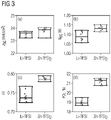
- figure 3 shows four different characteristic photovoltaic parameters (JSC (short circuit current), VOC (open circuit voltage), FF (fill factor) and PCE (photo current efficiency) of perovskite solar cells.
- JSC short circuit current
- VOC open circuit voltage
- FF fill factor
- PCE photo current efficiency
- figure 4 shows measurement of individual hole conductor layers without solar cell structure.
- the figure shows the current density of different doping concentrations at different voltages, with the result that from 0.2 mol of dopant per mol of matrix compound, a significant increase in the current density by increasing the doping concentration is obviously no longer possible.
- the Fill Factor denotes the quotient of the maximum power of a solar cell at the maximum power point and the product of open circuit voltage and short circuit current.
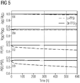
- the result of the measurements shows that the organometallic solar cells constructed with a hole conductor layer with the doping agent based on zinc and/or bismuth according to the invention and with an absorber layer made of a material that crystallizes in the three-dimensional perovskite structure have a very good efficiency of converting light into electricity -Show conversion.
- the present invention discloses for the first time a metal-organic solar cell, comprising an absorber layer with a compound that crystallizes in the perovskite crystal lattice, which has a lithium-poor hole conductor layer.
Landscapes
- Engineering & Computer Science (AREA)
- Chemical & Material Sciences (AREA)
- Power Engineering (AREA)
- Chemical Kinetics & Catalysis (AREA)
- Electrochemistry (AREA)
- Physics & Mathematics (AREA)
- Materials Engineering (AREA)
- Electromagnetism (AREA)
- Microelectronics & Electronic Packaging (AREA)
- Inorganic Chemistry (AREA)
- Manufacturing & Machinery (AREA)
- Life Sciences & Earth Sciences (AREA)
- Sustainable Development (AREA)
- Photovoltaic Devices (AREA)
- Inorganic Insulating Materials (AREA)
- Inorganic Compounds Of Heavy Metals (AREA)
Claims (13)
- Pile solaire organométallique, comprenant au moins deux couches (5, 7) de contact, dans laquelle une couche de contact est constituée en anode (5),
et, en étant voisine respectivement, une couche (2, 4) semiconductrice d'un empilement de couches ayant une couche (3) absorbante au milieu en un matériau organométallique, qui cristallise dans le réseau cristallin perovskite tridimensionnel, dans laquelle la couche (3) absorbante comprend du plomb comme atome central et un halogénure comme anion dans un composé organométallique, caractérisé en ce que la au moins une couche (4) semiconductrice entre la couche (3) absorbante et l'anode (5) est une couche de conduction par trou, qui comprend un agent de dopage contenant du zinc. - Pile solaire organométallique, comprenant au moins deux couches (5, 7) de contact, dans laquelle une couche de contact est constituée en anode (5),
et, en étant voisine respectivement, une couche (2, 4) semiconductrice d'un empilement de couches ayant une couche (3) absorbante au milieu en un matériau organométallique, qui cristallise dans le réseau cristallin perovskite tridimensionnel, dans laquelle la couche (3) absorbante comprend de l'étain comme atome central et un halogénure comme anion dans un composé organométallique, caractérisé en ce que la au moins une couche (4) semiconductrice entre la couche (3) absorbante et l'anode (5) est une couche à conduction par trou, qui comprend un agent de dopage contenant du bismuth. - Pile solaire suivant l'une des revendications 1 ou 2, dans laquelle l'agent de dopage composé du zinc ou du bismuth est le sel d'un peracide.
- Pile solaire suivant l'une des revendications 1 à 3, dans laquelle la pile solaire comprend une couche formant barrière de diffusion entre la couche absorbante et une couche semiconductrice.
- Pile solaire suivant la revendication 4, dans laquelle la couche formant barrière de diffusion a une épaisseur de couche plus petite que 150 nm.
- Pile solaire suivant l'une des revendications 1 à 5, qui comprend, dans la matière de matrice de la couche de la conduction par trou, un ou plusieurs composés choisis dans le groupe des composés suivants :spiro-OMeTAD - 2,2',7,7'-tétrakis-(N, N-di-p-méthoxyphénylamine) 9,9'-spirobifluorène,PEDOT - poly(3,4 éthylènedioxythiophène),PVK - poly(9-vinylcarbazole),PTPD - poly(N.N-bis(4-butylphényl)-N,N-bis(phényl - benzidine),P3HT - poly(3-hexylthiophène),PANI - polyaniline,PTAA - Poly[bis(4-phényl)(2,4,6-triméthylphényl)amine],9,9-Bis[4-(N, N-bis-biphényl-4-yl-amino)phényl)]-9H-fluorène, 4,4',4"-Tris(N-(2-naphtyl)-N-phényl- amino)triphénylamine,et / ou des liquides ioniques ainsi que des mélanges des composés mentionnés ci-dessus.
- Pile solaire suivant l'une des revendications 1 à 6, dans laquelle la couche absorbante comprend un complexe métallique ayant de l'étain et/ou du plomb comme atome central, qui contient au moins un anion sous la forme d'un halogénure ou d'un pseudo-halogénure choisi dans le groupe des éléments suivants : fluorure, chlorure, bromure, iodure, cyanure, isocyanure.
- Pile solaire suivant l'une des revendications 1 à 7, dans laquelle la couche absorbante comprend un complexe métallique ayant de l'étain et/ou du plomb comme atome central, auquel est coordinné un ligand- (CH3NH3)+.
- Pile solaire tandem comprenant au moins deux piles solaires mises l'une sur l'autre en un empilement de couches, dans laquelle une pile solaire est une pile solaire organométallique suivant l'une des revendications 1 à 8.
- Pile solaire tandem suivant la revendication 9, dans laquelle la pile solaire organométallique suivant l'une des revendications 1 à 9 est la pile solaire supérieure, sur laquelle les photons arrivent en premier.
- Pile solaire tandem suivant l'une des revendications 9 ou 10, qui comprend une pile solaire ayant du silicium cristallin dans la couche absorbante.
- Pile solaire tandem suivant l'une des revendications 9 à 11, qui comprend deux piles solaires organométalliques suivant l'une des revendications 1 à 8, dans laquelle les deux piles solaires sont différentes dans la composition de la matière, qui forme la couche absorbante.
- Procédé de préparation d'un corps stratifié, formant une pile solaire tandem, dans lequel un empilement de couches, comprenant deux piles solaires, peut être produit par dépôt de couches dans un procédé chimique en voie humide, dans lequel on prépare une pile solaire inférieure et une pile solaire supérieure par la production de couches se succédant l'une sur l'autre, caractérisé en ce que l'une des piles solaires est une pile solaire organométallique suivant l'une des revendications 1 à 8.
Applications Claiming Priority (2)
| Application Number | Priority Date | Filing Date | Title |
|---|---|---|---|
| DE102018212305.5A DE102018212305A1 (de) | 2018-07-24 | 2018-07-24 | Metallorganische Perowskit-Solarzelle, Tandem-Solarzelle sowie Herstellungsverfahren dazu |
| PCT/EP2019/068247 WO2020020620A1 (fr) | 2018-07-24 | 2019-07-08 | Cellule solaire à base de pérovskite organométallique, cellule solaire tandem et procédé de fabrication associé |
Publications (2)
| Publication Number | Publication Date |
|---|---|
| EP3797441A1 EP3797441A1 (fr) | 2021-03-31 |
| EP3797441B1 true EP3797441B1 (fr) | 2022-06-08 |
Family
ID=67480150
Family Applications (1)
| Application Number | Title | Priority Date | Filing Date |
|---|---|---|---|
| EP19745981.1A Active EP3797441B1 (fr) | 2018-07-24 | 2019-07-08 | Cellule solaire à base de pérovskite organométallique, cellule solaire tandem et procédé de fabrication associé |
Country Status (9)
| Country | Link |
|---|---|
| US (1) | US20210249196A1 (fr) |
| EP (1) | EP3797441B1 (fr) |
| CN (1) | CN112534596B (fr) |
| AU (1) | AU2019312457B2 (fr) |
| DE (1) | DE102018212305A1 (fr) |
| ES (1) | ES2926017T3 (fr) |
| MA (1) | MA52711B1 (fr) |
| SA (1) | SA521421077B1 (fr) |
| WO (1) | WO2020020620A1 (fr) |
Families Citing this family (2)
| Publication number | Priority date | Publication date | Assignee | Title |
|---|---|---|---|---|
| CN113707816B (zh) * | 2021-08-24 | 2023-07-04 | 江苏盛开高新材料有限公司 | 一种钙钛矿太阳能电池的制备方法 |
| WO2024054299A2 (fr) * | 2022-07-16 | 2024-03-14 | Board Of Trustees Of Michigan State University | Sels organiques multivalents pour photovoltaïque |
Family Cites Families (14)
| Publication number | Priority date | Publication date | Assignee | Title |
|---|---|---|---|---|
| DE102009022117A1 (de) | 2009-05-20 | 2010-11-25 | Siemens Aktiengesellschaft | Material für eine Lochtransportschicht mit p-Dotierung |
| DE102011003192B4 (de) | 2011-01-26 | 2015-12-24 | Siemens Aktiengesellschaft | Halbleiterbauelement und Verfahren zu seiner Herstellung |
| DE102011013897A1 (de) | 2011-03-11 | 2012-09-13 | Technische Universität Dresden | Organische Solarzelle |
| DE102012209520A1 (de) | 2012-06-06 | 2013-12-12 | Osram Opto Semiconductors Gmbh | Metallkomplexe als p-Dotanden für organische elektronische Matrixmaterialien |
| EP2693503A1 (fr) | 2012-08-03 | 2014-02-05 | Ecole Polytechnique Fédérale de Lausanne (EPFL) | Cellule solaire à hétérojonction comprenant une couche pérovskite d'halogénures organo-métalliques et sa fabrication |
| AU2013319979B2 (en) | 2012-09-18 | 2016-08-25 | Oxford Photovoltaics Limited | Optoelectronic device |
| GB201309668D0 (en) * | 2013-05-30 | 2013-07-17 | Isis Innovation | Organic semiconductor doping process |
| EP3132472A1 (fr) * | 2014-04-15 | 2017-02-22 | Northwestern University | Cellules photovoltaïques à pérovskite organique-inorganique d'halogénure à semi-conducteurs sans plomb |
| DE102014210412A1 (de) | 2014-06-03 | 2015-12-03 | Siemens Aktiengesellschaft | p-Dotierende Vernetzung organischer Lochleiter |
| DE102015121844A1 (de) * | 2015-12-15 | 2017-06-22 | Osram Oled Gmbh | Organisches elektronisches Bauelement und Verwendung eines fluorierten Sulfonimid-Metallsalzes |
| WO2018005749A1 (fr) * | 2016-06-29 | 2018-01-04 | Alliance For Sustainable Energy, Llc | Procédés de fabrication de cellules solaires en pérovskite ayant des couches de transport de trous améliorées |
| WO2018007586A1 (fr) * | 2016-07-07 | 2018-01-11 | Technische Universiteit Eindhoven | Couche barrière de passivation en contact avec de la pérovskite pour cellules solaires |
| KR20180047382A (ko) * | 2016-10-31 | 2018-05-10 | 고려대학교 산학협력단 | 확산 방지막을 이용한 페로브스카이트 태양전지 및 이의 제조방법 |
| CN108063186A (zh) * | 2017-11-20 | 2018-05-22 | 济南大学 | 锌掺杂氧化镍空穴传输层反置钙钛矿太阳能电池及制备方法 |
-
2018
- 2018-07-24 DE DE102018212305.5A patent/DE102018212305A1/de not_active Withdrawn
-
2019
- 2019-07-08 ES ES19745981T patent/ES2926017T3/es active Active
- 2019-07-08 EP EP19745981.1A patent/EP3797441B1/fr active Active
- 2019-07-08 AU AU2019312457A patent/AU2019312457B2/en active Active
- 2019-07-08 WO PCT/EP2019/068247 patent/WO2020020620A1/fr not_active Ceased
- 2019-07-08 CN CN201980049175.2A patent/CN112534596B/zh active Active
- 2019-07-08 US US17/261,001 patent/US20210249196A1/en not_active Abandoned
- 2019-07-08 MA MA52711A patent/MA52711B1/fr unknown
-
2021
- 2021-01-21 SA SA521421077A patent/SA521421077B1/ar unknown
Also Published As
| Publication number | Publication date |
|---|---|
| AU2019312457B2 (en) | 2021-05-27 |
| WO2020020620A1 (fr) | 2020-01-30 |
| DE102018212305A1 (de) | 2020-01-30 |
| EP3797441A1 (fr) | 2021-03-31 |
| ES2926017T3 (es) | 2022-10-21 |
| MA52711A (fr) | 2021-03-31 |
| CN112534596A (zh) | 2021-03-19 |
| MA52711B1 (fr) | 2022-08-31 |
| AU2019312457A1 (en) | 2021-02-11 |
| SA521421077B1 (ar) | 2025-04-20 |
| CN112534596B (zh) | 2023-09-12 |
| US20210249196A1 (en) | 2021-08-12 |
Similar Documents
| Publication | Publication Date | Title |
|---|---|---|
| Yang et al. | Achievements, challenges, and future prospects for industrialization of perovskite solar cells | |
| US11335513B2 (en) | Passivation of defects in perovskite materials for improved solar cell efficiency and stability | |
| Tiep et al. | Recent advances in improving the stability of perovskite solar cells | |
| DE102007018456B4 (de) | Verwendung von Hauptgruppenelementhalogeniden und/oder -pseudohalogeniden, organisches halbleitendes Matrixmaterial, elektronische und optoelektronische Bauelemente | |
| US10332688B2 (en) | Methods for making perovskite solar cells having improved hole-transport layers | |
| DE102008051737B4 (de) | Quadratisch planare Übergangsmetallkomplexe, organische halbleitende Materialien sowie elektronische oder optoelektronische Bauelemente, die diese umfassen und Verwendung derselben | |
| JP6935175B2 (ja) | 膜、光デバイス、電子デバイス、光電変換装置、および膜の製造方法 | |
| KR20190141742A (ko) | 장기 고 가동 안정성을 갖는 무기 홀 도체 기초 퍼로브스카이트 광전 전환 장치 | |
| WO2007134873A1 (fr) | Utilisation de complexes de métaux transitoires planaires quadratiques comme dopants | |
| EP2002492A1 (fr) | Utilisation de radicaux heterocycliques pour le dopage de semi-conducteurs organiques | |
| EP3385269B1 (fr) | Pérovskite hybride organique-inorganique, procédé de préparation de celle-ci, et cellule solaire comprenant celle-ci | |
| DE112020007073T5 (de) | Verarbeitung von effizienten perovskit-solarzellen in feuchter luft basierend auf polymerisierbaren ionischen flüssigkeiten und salzen | |
| DE102006054523B4 (de) | Dithiolenübergangsmetallkomplexe und Selen-analoge Verbindungen, deren Verwendung als Dotand, organisches halbleitendes Material enthaltend die Komplexe, sowie elektronische oder optoelektronisches Bauelement enthaltend einen Komplex | |
| EP2659529B1 (fr) | Composant optoélectronique à couches dopées | |
| EP3797441B1 (fr) | Cellule solaire à base de pérovskite organométallique, cellule solaire tandem et procédé de fabrication associé | |
| Jamesh et al. | Advancement of technology towards developing perovskite-based solar cells for renewable energy harvesting and energy transformation applications | |
| EP2132800B1 (fr) | Dispositif organique à émission de rayonnements et procédé pour le produire | |
| WO2020020622A1 (fr) | Cellule solaire à base de pérovskite organométallique, cellule solaire tandem et procédé de fabrication associé | |
| US12334279B2 (en) | Compositions and methods for modifying perovskite surfaces | |
| CN118475207A (zh) | 钙钛矿太阳能电池及其制备方法、叠层电池 | |
| WO2016116205A1 (fr) | Proazaphosphatranes en tant qu'agents de dopage de type n en électronique organique | |
| KR102022688B1 (ko) | 흡수체로서 3-피콜리뉴밀암모늄을 포함하는 화합물, 이의 제조 방법 및 이를 포함하는 태양전지 |
Legal Events
| Date | Code | Title | Description |
|---|---|---|---|
| STAA | Information on the status of an ep patent application or granted ep patent |
Free format text: STATUS: UNKNOWN |
|
| STAA | Information on the status of an ep patent application or granted ep patent |
Free format text: STATUS: THE INTERNATIONAL PUBLICATION HAS BEEN MADE |
|
| PUAI | Public reference made under article 153(3) epc to a published international application that has entered the european phase |
Free format text: ORIGINAL CODE: 0009012 |
|
| STAA | Information on the status of an ep patent application or granted ep patent |
Free format text: STATUS: REQUEST FOR EXAMINATION WAS MADE |
|
| 17P | Request for examination filed |
Effective date: 20201222 |
|
| AK | Designated contracting states |
Kind code of ref document: A1 Designated state(s): AL AT BE BG CH CY CZ DE DK EE ES FI FR GB GR HR HU IE IS IT LI LT LU LV MC MK MT NL NO PL PT RO RS SE SI SK SM TR |
|
| AX | Request for extension of the european patent |
Extension state: BA ME |
|
| RAP1 | Party data changed (applicant data changed or rights of an application transferred) |
Owner name: SIEMENS ENERGY GLOBAL GMBH & CO. KG |
|
| DAX | Request for extension of the european patent (deleted) | ||
| RAV | Requested validation state of the european patent: fee paid |
Extension state: TN Effective date: 20201222 Extension state: MA Effective date: 20201222 |
|
| GRAP | Despatch of communication of intention to grant a patent |
Free format text: ORIGINAL CODE: EPIDOSNIGR1 |
|
| STAA | Information on the status of an ep patent application or granted ep patent |
Free format text: STATUS: GRANT OF PATENT IS INTENDED |
|
| INTG | Intention to grant announced |
Effective date: 20220127 |
|
| GRAS | Grant fee paid |
Free format text: ORIGINAL CODE: EPIDOSNIGR3 |
|
| GRAA | (expected) grant |
Free format text: ORIGINAL CODE: 0009210 |
|
| STAA | Information on the status of an ep patent application or granted ep patent |
Free format text: STATUS: THE PATENT HAS BEEN GRANTED |
|
| AK | Designated contracting states |
Kind code of ref document: B1 Designated state(s): AL AT BE BG CH CY CZ DE DK EE ES FI FR GB GR HR HU IE IS IT LI LT LU LV MC MK MT NL NO PL PT RO RS SE SI SK SM TR |
|
| REG | Reference to a national code |
Ref country code: TN Ref legal event code: VAGR Ref document number: TN/P/2022/000296 Country of ref document: TN |
|
| REG | Reference to a national code |
Ref country code: AT Ref legal event code: REF Ref document number: 1497537 Country of ref document: AT Kind code of ref document: T Effective date: 20220615 Ref country code: CH Ref legal event code: EP |
|
| REG | Reference to a national code |
Ref country code: DE Ref legal event code: R096 Ref document number: 502019004601 Country of ref document: DE |
|
| REG | Reference to a national code |
Ref country code: IE Ref legal event code: FG4D Free format text: LANGUAGE OF EP DOCUMENT: GERMAN |
|
| REG | Reference to a national code |
Ref country code: MA Ref legal event code: VAGR Ref document number: 52711 Country of ref document: MA Kind code of ref document: B1 |
|
| REG | Reference to a national code |
Ref country code: LT Ref legal event code: MG9D |
|
| REG | Reference to a national code |
Ref country code: NL Ref legal event code: MP Effective date: 20220608 |
|
| REG | Reference to a national code |
Ref country code: ES Ref legal event code: FG2A Ref document number: 2926017 Country of ref document: ES Kind code of ref document: T3 Effective date: 20221021 |
|
| PG25 | Lapsed in a contracting state [announced via postgrant information from national office to epo] |
Ref country code: SE Free format text: LAPSE BECAUSE OF FAILURE TO SUBMIT A TRANSLATION OF THE DESCRIPTION OR TO PAY THE FEE WITHIN THE PRESCRIBED TIME-LIMIT Effective date: 20220608 Ref country code: NO Free format text: LAPSE BECAUSE OF FAILURE TO SUBMIT A TRANSLATION OF THE DESCRIPTION OR TO PAY THE FEE WITHIN THE PRESCRIBED TIME-LIMIT Effective date: 20220908 Ref country code: LT Free format text: LAPSE BECAUSE OF FAILURE TO SUBMIT A TRANSLATION OF THE DESCRIPTION OR TO PAY THE FEE WITHIN THE PRESCRIBED TIME-LIMIT Effective date: 20220608 Ref country code: HR Free format text: LAPSE BECAUSE OF FAILURE TO SUBMIT A TRANSLATION OF THE DESCRIPTION OR TO PAY THE FEE WITHIN THE PRESCRIBED TIME-LIMIT Effective date: 20220608 Ref country code: GR Free format text: LAPSE BECAUSE OF FAILURE TO SUBMIT A TRANSLATION OF THE DESCRIPTION OR TO PAY THE FEE WITHIN THE PRESCRIBED TIME-LIMIT Effective date: 20220909 Ref country code: FI Free format text: LAPSE BECAUSE OF FAILURE TO SUBMIT A TRANSLATION OF THE DESCRIPTION OR TO PAY THE FEE WITHIN THE PRESCRIBED TIME-LIMIT Effective date: 20220608 Ref country code: BG Free format text: LAPSE BECAUSE OF FAILURE TO SUBMIT A TRANSLATION OF THE DESCRIPTION OR TO PAY THE FEE WITHIN THE PRESCRIBED TIME-LIMIT Effective date: 20220908 |
|
| REG | Reference to a national code |
Ref country code: DE Ref legal event code: R079 Ref document number: 502019004601 Country of ref document: DE Free format text: PREVIOUS MAIN CLASS: H01L0051420000 Ipc: H10K0030000000 |
|
| PG25 | Lapsed in a contracting state [announced via postgrant information from national office to epo] |
Ref country code: RS Free format text: LAPSE BECAUSE OF FAILURE TO SUBMIT A TRANSLATION OF THE DESCRIPTION OR TO PAY THE FEE WITHIN THE PRESCRIBED TIME-LIMIT Effective date: 20220608 Ref country code: LV Free format text: LAPSE BECAUSE OF FAILURE TO SUBMIT A TRANSLATION OF THE DESCRIPTION OR TO PAY THE FEE WITHIN THE PRESCRIBED TIME-LIMIT Effective date: 20220608 |
|
| PG25 | Lapsed in a contracting state [announced via postgrant information from national office to epo] |
Ref country code: NL Free format text: LAPSE BECAUSE OF FAILURE TO SUBMIT A TRANSLATION OF THE DESCRIPTION OR TO PAY THE FEE WITHIN THE PRESCRIBED TIME-LIMIT Effective date: 20220608 |
|
| PG25 | Lapsed in a contracting state [announced via postgrant information from national office to epo] |
Ref country code: SM Free format text: LAPSE BECAUSE OF FAILURE TO SUBMIT A TRANSLATION OF THE DESCRIPTION OR TO PAY THE FEE WITHIN THE PRESCRIBED TIME-LIMIT Effective date: 20220608 Ref country code: SK Free format text: LAPSE BECAUSE OF FAILURE TO SUBMIT A TRANSLATION OF THE DESCRIPTION OR TO PAY THE FEE WITHIN THE PRESCRIBED TIME-LIMIT Effective date: 20220608 Ref country code: RO Free format text: LAPSE BECAUSE OF FAILURE TO SUBMIT A TRANSLATION OF THE DESCRIPTION OR TO PAY THE FEE WITHIN THE PRESCRIBED TIME-LIMIT Effective date: 20220608 Ref country code: PT Free format text: LAPSE BECAUSE OF FAILURE TO SUBMIT A TRANSLATION OF THE DESCRIPTION OR TO PAY THE FEE WITHIN THE PRESCRIBED TIME-LIMIT Effective date: 20221010 Ref country code: EE Free format text: LAPSE BECAUSE OF FAILURE TO SUBMIT A TRANSLATION OF THE DESCRIPTION OR TO PAY THE FEE WITHIN THE PRESCRIBED TIME-LIMIT Effective date: 20220608 Ref country code: CZ Free format text: LAPSE BECAUSE OF FAILURE TO SUBMIT A TRANSLATION OF THE DESCRIPTION OR TO PAY THE FEE WITHIN THE PRESCRIBED TIME-LIMIT Effective date: 20220608 |
|
| PG25 | Lapsed in a contracting state [announced via postgrant information from national office to epo] |
Ref country code: PL Free format text: LAPSE BECAUSE OF FAILURE TO SUBMIT A TRANSLATION OF THE DESCRIPTION OR TO PAY THE FEE WITHIN THE PRESCRIBED TIME-LIMIT Effective date: 20220608 Ref country code: IS Free format text: LAPSE BECAUSE OF FAILURE TO SUBMIT A TRANSLATION OF THE DESCRIPTION OR TO PAY THE FEE WITHIN THE PRESCRIBED TIME-LIMIT Effective date: 20221008 |
|
| REG | Reference to a national code |
Ref country code: CH Ref legal event code: PL |
|
| RAP4 | Party data changed (patent owner data changed or rights of a patent transferred) |
Owner name: SIEMENS ENERGY GLOBAL GMBH & CO. KG |
|
| REG | Reference to a national code |
Ref country code: DE Ref legal event code: R097 Ref document number: 502019004601 Country of ref document: DE |
|
| REG | Reference to a national code |
Ref country code: BE Ref legal event code: MM Effective date: 20220731 |
|
| PG25 | Lapsed in a contracting state [announced via postgrant information from national office to epo] |
Ref country code: MC Free format text: LAPSE BECAUSE OF FAILURE TO SUBMIT A TRANSLATION OF THE DESCRIPTION OR TO PAY THE FEE WITHIN THE PRESCRIBED TIME-LIMIT Effective date: 20220608 Ref country code: AL Free format text: LAPSE BECAUSE OF FAILURE TO SUBMIT A TRANSLATION OF THE DESCRIPTION OR TO PAY THE FEE WITHIN THE PRESCRIBED TIME-LIMIT Effective date: 20220608 |
|
| PLBE | No opposition filed within time limit |
Free format text: ORIGINAL CODE: 0009261 |
|
| STAA | Information on the status of an ep patent application or granted ep patent |
Free format text: STATUS: NO OPPOSITION FILED WITHIN TIME LIMIT |
|
| PG25 | Lapsed in a contracting state [announced via postgrant information from national office to epo] |
Ref country code: LU Free format text: LAPSE BECAUSE OF NON-PAYMENT OF DUE FEES Effective date: 20220708 Ref country code: LI Free format text: LAPSE BECAUSE OF NON-PAYMENT OF DUE FEES Effective date: 20220731 Ref country code: DK Free format text: LAPSE BECAUSE OF FAILURE TO SUBMIT A TRANSLATION OF THE DESCRIPTION OR TO PAY THE FEE WITHIN THE PRESCRIBED TIME-LIMIT Effective date: 20220608 Ref country code: CH Free format text: LAPSE BECAUSE OF NON-PAYMENT OF DUE FEES Effective date: 20220731 |
|
| 26N | No opposition filed |
Effective date: 20230310 |
|
| PG25 | Lapsed in a contracting state [announced via postgrant information from national office to epo] |
Ref country code: SI Free format text: LAPSE BECAUSE OF FAILURE TO SUBMIT A TRANSLATION OF THE DESCRIPTION OR TO PAY THE FEE WITHIN THE PRESCRIBED TIME-LIMIT Effective date: 20220608 Ref country code: BE Free format text: LAPSE BECAUSE OF NON-PAYMENT OF DUE FEES Effective date: 20220731 |
|
| PG25 | Lapsed in a contracting state [announced via postgrant information from national office to epo] |
Ref country code: IE Free format text: LAPSE BECAUSE OF NON-PAYMENT OF DUE FEES Effective date: 20220708 Ref country code: FR Free format text: LAPSE BECAUSE OF NON-PAYMENT OF DUE FEES Effective date: 20220808 |
|
| VSFP | Annual fee paid to validation state [announced via postgrant information from national office to epo] |
Ref country code: TN Payment date: 20220731 Year of fee payment: 4 |
|
| GBPC | Gb: european patent ceased through non-payment of renewal fee |
Effective date: 20230708 |
|
| PG25 | Lapsed in a contracting state [announced via postgrant information from national office to epo] |
Ref country code: MK Free format text: LAPSE BECAUSE OF FAILURE TO SUBMIT A TRANSLATION OF THE DESCRIPTION OR TO PAY THE FEE WITHIN THE PRESCRIBED TIME-LIMIT Effective date: 20220608 Ref country code: CY Free format text: LAPSE BECAUSE OF FAILURE TO SUBMIT A TRANSLATION OF THE DESCRIPTION OR TO PAY THE FEE WITHIN THE PRESCRIBED TIME-LIMIT Effective date: 20220608 Ref country code: GB Free format text: LAPSE BECAUSE OF NON-PAYMENT OF DUE FEES Effective date: 20230708 |
|
| PG25 | Lapsed in a contracting state [announced via postgrant information from national office to epo] |
Ref country code: HU Free format text: LAPSE BECAUSE OF FAILURE TO SUBMIT A TRANSLATION OF THE DESCRIPTION OR TO PAY THE FEE WITHIN THE PRESCRIBED TIME-LIMIT; INVALID AB INITIO Effective date: 20190708 |
|
| PG25 | Lapsed in a contracting state [announced via postgrant information from national office to epo] |
Ref country code: MT Free format text: LAPSE BECAUSE OF FAILURE TO SUBMIT A TRANSLATION OF THE DESCRIPTION OR TO PAY THE FEE WITHIN THE PRESCRIBED TIME-LIMIT Effective date: 20220608 |
|
| PG25 | Lapsed in a contracting state [announced via postgrant information from national office to epo] |
Ref country code: BG Free format text: LAPSE BECAUSE OF FAILURE TO SUBMIT A TRANSLATION OF THE DESCRIPTION OR TO PAY THE FEE WITHIN THE PRESCRIBED TIME-LIMIT Effective date: 20220608 |
|
| PG25 | Lapsed in a contracting state [announced via postgrant information from national office to epo] |
Ref country code: BG Free format text: LAPSE BECAUSE OF FAILURE TO SUBMIT A TRANSLATION OF THE DESCRIPTION OR TO PAY THE FEE WITHIN THE PRESCRIBED TIME-LIMIT Effective date: 20220608 |
|
| PGFP | Annual fee paid to national office [announced via postgrant information from national office to epo] |
Ref country code: TR Payment date: 20250619 Year of fee payment: 7 |
|
| REG | Reference to a national code |
Ref country code: AT Ref legal event code: MM01 Ref document number: 1497537 Country of ref document: AT Kind code of ref document: T Effective date: 20240708 |
|
| PGFP | Annual fee paid to national office [announced via postgrant information from national office to epo] |
Ref country code: ES Payment date: 20250812 Year of fee payment: 7 |
|
| PGFP | Annual fee paid to national office [announced via postgrant information from national office to epo] |
Ref country code: DE Payment date: 20250728 Year of fee payment: 7 |
|
| PGFP | Annual fee paid to national office [announced via postgrant information from national office to epo] |
Ref country code: IT Payment date: 20250721 Year of fee payment: 7 |
|
| PG25 | Lapsed in a contracting state [announced via postgrant information from national office to epo] |
Ref country code: AT Free format text: LAPSE BECAUSE OF NON-PAYMENT OF DUE FEES Effective date: 20240708 |
|
| VSFP | Annual fee paid to validation state [announced via postgrant information from national office to epo] |
Ref country code: MA Payment date: 20230704 Year of fee payment: 5 |
|
| VSFP | Annual fee paid to validation state [announced via postgrant information from national office to epo] |
Ref country code: MA Payment date: 20220701 Year of fee payment: 4 |
|
| VSFP | Annual fee paid to validation state [announced via postgrant information from national office to epo] |
Ref country code: MA Payment date: 20240701 Year of fee payment: 6 |
|
| VSFP | Annual fee paid to validation state [announced via postgrant information from national office to epo] |
Ref country code: MA Payment date: 20250813 Year of fee payment: 7 |
|
| PGFP | Annual fee paid to national office [announced via postgrant information from national office to epo] |
Ref country code: AT Payment date: 20260410 Year of fee payment: 5 |