EP3799108A1 - Lentille d'entrée et spectromètre d'électrons - Google Patents
Lentille d'entrée et spectromètre d'électrons Download PDFInfo
- Publication number
- EP3799108A1 EP3799108A1 EP20198606.4A EP20198606A EP3799108A1 EP 3799108 A1 EP3799108 A1 EP 3799108A1 EP 20198606 A EP20198606 A EP 20198606A EP 3799108 A1 EP3799108 A1 EP 3799108A1
- Authority
- EP
- European Patent Office
- Prior art keywords
- input lens
- electrode
- electron
- mesh
- electrons
- Prior art date
- Legal status (The legal status is an assumption and is not a legal conclusion. Google has not performed a legal analysis and makes no representation as to the accuracy of the status listed.)
- Withdrawn
Links
Images

Classifications
-
- H—ELECTRICITY
- H01—ELECTRIC ELEMENTS
- H01J—ELECTRIC DISCHARGE TUBES OR DISCHARGE LAMPS
- H01J49/00—Particle spectrometers or separator tubes
- H01J49/02—Details
- H01J49/06—Electron- or ion-optical arrangements
- H01J49/068—Mounting, supporting, spacing, or insulating electrodes
-
- H—ELECTRICITY
- H01—ELECTRIC ELEMENTS
- H01J—ELECTRIC DISCHARGE TUBES OR DISCHARGE LAMPS
- H01J49/00—Particle spectrometers or separator tubes
- H01J49/02—Details
- H01J49/06—Electron- or ion-optical arrangements
- H01J49/067—Ion lenses, apertures, skimmers
-
- H—ELECTRICITY
- H01—ELECTRIC ELEMENTS
- H01J—ELECTRIC DISCHARGE TUBES OR DISCHARGE LAMPS
- H01J37/00—Discharge tubes with provision for introducing objects or material to be exposed to the discharge, e.g. for the purpose of examination or processing thereof
- H01J37/02—Details
- H01J37/04—Arrangements of electrodes and associated parts for generating or controlling the discharge, e.g. electron-optical arrangement or ion-optical arrangement
- H01J37/05—Electron or ion-optical arrangements for separating electrons or ions according to their energy or mass
-
- H—ELECTRICITY
- H01—ELECTRIC ELEMENTS
- H01J—ELECTRIC DISCHARGE TUBES OR DISCHARGE LAMPS
- H01J37/00—Discharge tubes with provision for introducing objects or material to be exposed to the discharge, e.g. for the purpose of examination or processing thereof
- H01J37/02—Details
- H01J37/04—Arrangements of electrodes and associated parts for generating or controlling the discharge, e.g. electron-optical arrangement or ion-optical arrangement
- H01J37/10—Lenses
- H01J37/12—Lenses electrostatic
-
- H—ELECTRICITY
- H01—ELECTRIC ELEMENTS
- H01J—ELECTRIC DISCHARGE TUBES OR DISCHARGE LAMPS
- H01J37/00—Discharge tubes with provision for introducing objects or material to be exposed to the discharge, e.g. for the purpose of examination or processing thereof
- H01J37/02—Details
- H01J37/04—Arrangements of electrodes and associated parts for generating or controlling the discharge, e.g. electron-optical arrangement or ion-optical arrangement
- H01J37/153—Electron-optical or ion-optical arrangements for the correction of image defects, e.g. stigmators
-
- H—ELECTRICITY
- H01—ELECTRIC ELEMENTS
- H01J—ELECTRIC DISCHARGE TUBES OR DISCHARGE LAMPS
- H01J49/00—Particle spectrometers or separator tubes
- H01J49/44—Energy spectrometers, e.g. alpha-, beta-spectrometers
-
- G—PHYSICS
- G01—MEASURING; TESTING
- G01N—INVESTIGATING OR ANALYSING MATERIALS BY DETERMINING THEIR CHEMICAL OR PHYSICAL PROPERTIES
- G01N23/00—Investigating or analysing materials by the use of wave or particle radiation, e.g. X-rays or neutrons, not covered by groups G01N3/00 – G01N17/00, G01N21/00 or G01N22/00
- G01N23/22—Investigating or analysing materials by the use of wave or particle radiation, e.g. X-rays or neutrons, not covered by groups G01N3/00 – G01N17/00, G01N21/00 or G01N22/00 by measuring secondary emission from the material
- G01N23/227—Measuring photoelectric effect, e.g. photoelectron emission microscopy [PEEM]
-
- H—ELECTRICITY
- H01—ELECTRIC ELEMENTS
- H01J—ELECTRIC DISCHARGE TUBES OR DISCHARGE LAMPS
- H01J2237/00—Discharge tubes exposing object to beam, e.g. for analysis treatment, etching, imaging
- H01J2237/02—Details
- H01J2237/026—Shields
- H01J2237/0262—Shields electrostatic
-
- H—ELECTRICITY
- H01—ELECTRIC ELEMENTS
- H01J—ELECTRIC DISCHARGE TUBES OR DISCHARGE LAMPS
- H01J2237/00—Discharge tubes exposing object to beam, e.g. for analysis treatment, etching, imaging
- H01J2237/05—Arrangements for energy or mass analysis
-
- H—ELECTRICITY
- H01—ELECTRIC ELEMENTS
- H01J—ELECTRIC DISCHARGE TUBES OR DISCHARGE LAMPS
- H01J2237/00—Discharge tubes exposing object to beam, e.g. for analysis treatment, etching, imaging
- H01J2237/10—Lenses
- H01J2237/12—Lenses electrostatic
- H01J2237/121—Lenses electrostatic characterised by shape
-
- H—ELECTRICITY
- H01—ELECTRIC ELEMENTS
- H01J—ELECTRIC DISCHARGE TUBES OR DISCHARGE LAMPS
- H01J2237/00—Discharge tubes exposing object to beam, e.g. for analysis treatment, etching, imaging
- H01J2237/153—Correcting image defects, e.g. stigmators
-
- H—ELECTRICITY
- H01—ELECTRIC ELEMENTS
- H01J—ELECTRIC DISCHARGE TUBES OR DISCHARGE LAMPS
- H01J2237/00—Discharge tubes exposing object to beam, e.g. for analysis treatment, etching, imaging
- H01J2237/153—Correcting image defects, e.g. stigmators
- H01J2237/1534—Aberrations
-
- H—ELECTRICITY
- H01—ELECTRIC ELEMENTS
- H01J—ELECTRIC DISCHARGE TUBES OR DISCHARGE LAMPS
- H01J2237/00—Discharge tubes exposing object to beam, e.g. for analysis treatment, etching, imaging
- H01J2237/25—Tubes for localised analysis using electron or ion beams
- H01J2237/2505—Tubes for localised analysis using electron or ion beams characterised by their application
- H01J2237/2516—Secondary particles mass or energy spectrometry
- H01J2237/2522—Secondary particles mass or energy spectrometry of electrons (ESCA, XPS)
-
- H—ELECTRICITY
- H01—ELECTRIC ELEMENTS
- H01J—ELECTRIC DISCHARGE TUBES OR DISCHARGE LAMPS
- H01J49/00—Particle spectrometers or separator tubes
- H01J49/44—Energy spectrometers, e.g. alpha-, beta-spectrometers
- H01J49/46—Static spectrometers
- H01J49/48—Static spectrometers using electrostatic analysers, e.g. cylindrical sector, Wien filter
- H01J49/484—Static spectrometers using electrostatic analysers, e.g. cylindrical sector, Wien filter with spherical mirrors
Definitions
- the present invention relates to an input lens and electron spectrometer.
- electron spectroscopy is performed.
- One known electron analyzer for allowing for such electron spectroscopy is a hemispherical analyzer.
- an input lens is disposed between an electron source and the electron analyzer.
- the input lens has various functions including decelerating electrons, focusing electrons, converting image magnification factors, and others.
- Patent document 1 discloses an input lens comprising: a mesh disposed to form a magnified virtual image having a negative spherical aberration for electrons leaving a given object plane position with a given angular aperture, the mesh consisting of an ellipsoid of revolution that is recessed relative to the object plane and symmetrical with respect to the optical axis; and a lens system including electrodes arranged coaxially with the optical axis on the image plane side and forming a real image of the magnified virtual image.
- the electrodes consist of coaxial planes which together generate a focusing electric field that creates a positive spherical aberration.
- the acceptance solid angle for electrons is increased to the order of ⁇ 60 degrees by the use of an aspherical mesh which is an ellipsoid of revolution whose major axis lies in the direction of the optical axis.
- the ratio of the radius of the major axis to the radius of the minor axis in the ellipsoid of revolution is set to 1.5 to 2.
- Patent Document 1 Japanese Patent No. 4,802,340
- This electron spectrometer includes the input lens having a large acceptance solid angle for electrons and so electrons can be detected with improved sensitivity.
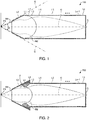
- FIG. 1 is a schematic cross-sectional view of the input lens, 100, associated with the first embodiment.
- FIG. 1 electron trajectories are indicated by broken lines.
- the input lens 100 is for use in an electron spectrometer having an electron source P1 and an electron analyzer, and is disposed between the electron source P1 and the electron analyzer in the spectrometer.
- the input lens 100 includes a reference electrode L0, a first electrode L1, a second electrode L2, a third electrode L3, a fourth electrode L4, a fifth electrode L5, ..., an ( n - 1)th electrode L n -1 , an n th electrode L n , a first mesh M1, a second mesh M2, and a slit S.
- the first mesh M1 is one example of another mesh referred to herein.
- the second mesh M2 is one example of a mesh referred to herein.
- the reference electrode L0 is positioned on the side of the electron source P1.
- the reference electrode L0 forms an entrance for electrons and is shaped cylindrically.
- the reference electrode L0 is in the form of a truncated cone.
- the potential of the reference electrode L0 is a reference potential.
- the reference potential is ground potential.
- the first mesh M1 is attached to the reference electrode L0.
- the optical axis O of the input lens 100 is the central axis of the reference electrode L0, for example.
- the first through n th electrodes L1 to L n are disposed between the reference electrode L0 and the slit S and arranged in this order along the optical axis O.
- the first through nth electrodes L1 to L n are in a tubular form, for example. In the illustrated example, they are cylindrical in shape.
- the optical axis O is a central axis, for example, of the first through nth electrodes L1 to L n .
- the optical axis O is the central axis common to the reference electrode L0 and to the first through n th electrodes L1 to L n . It suffices that the input lens 100 has three electrodes. That is, n is an integer equal to or greater than three.
- the first through n th electrodes L1 to L n are located inside a circular cone whose generatrix is a straight line G connecting the electron source P1 and the entrance-side end of the reference electrode L0.
- the first through n th electrodes L1 to L n may be located outside the circular cone in a manner not illustrated.
- the first electrode L1 is at a positive potential higher than that of the reference electrode L0.
- a positive voltage is applied to the first electrode L1.
- the potentials of the second to nth electrodes L2 to L n can be set according to electron spectroscopy conditions.
- a positive or negative voltage is applied to each of the second to nth electrodes L2 to L n .
- the voltages applied to the first through n th electrodes L1 to L n are variable, for example.
- the input lens 100 has a voltage source (not shown) for applying the voltages to the first through n th electrodes L1 to L n .
- the first mesh M1 is located at the entrance of the input lens 100 for electrons and attached to the reference electrode L0.
- the first mesh M1 is at the same potential as the reference electrode L0. That is, the potential of the first mesh M1 is ground potential.
- the first mesh M1 is a planar mesh and constitutes an electrostatic shield. The first mesh M1 serves to reduce leakage of electric fields from the front end of the input lens 100.
- the second mesh M2 is attached to the first electrode L1 and at the same potential as the first electrode L1. That is, the second mesh M2 is at a higher potential than the reference electrode L0.
- the second mesh M2 is shaped concavely relative to the electron source P1.
- the shape of the second mesh M2 is defined, for example, by a solid of revolution about the optical axis O.
- One example of the solid of revolution is an ellipsoid of revolution about the optical axis O.
- the second mesh M2 may be an aspherical mesh obtained by finely adjusting the shape of an ellipsoid of revolution so as to minimize the spherical aberration.
- the ratio a / b of the major axis a to the minor axis b of the ellipsoid of revolution of the second mesh M2 may be so set as to lie in the range of 1.5 to 2.0. Consequently, the acceptance solid angle ⁇ for electrons can be increased, for example, as compared with the case where the second mesh M2 is spherical in shape (see the above-cited Japanese Patent No. 4,802,340 ).
- the slit S is at the output of the input lens 100. That is, the slit S forms an exit of the input lens 100 for electrons. Electrons exit from the input lens 100 through the slit S.
- the second mesh M2 is attached to the first electrode L1. Additionally, another mesh similar to the second mesh M2 may be attached to at least one of the second to n th electrodes L2-L n .
- Electrons emanating from the electron source P1 enter the input lens 100. There is no potential gradient from the electron source P1 to the first mesh M1. Therefore, the electron trajectory between the electron source P1 and the first mesh M1 is linear. Electrons generated from the electron source P1 pass through the first mesh M1 and enter the input lens 100.
- the positive voltage is applied to the second mesh M2 to thereby create an electric field between the first mesh M1 and the second mesh M2, i.e., between the reference electrode L0 and the second mesh M2.
- This electric field creates a convex lens in an accelerating field. Consequently, between the first mesh M1 and the second mesh M2, electrons are attracted toward the optical axis O.
- the acceptance solid angle ⁇ for electrons can be increased, for example, as compared with the case where the potential of the second mesh M2 is the reference potential.
- the electric fields set up by the second to n th electrodes L2 to L n produce an electrostatic lens system between the second mesh M2 and the slit S.
- the potential of the reference electrode L0 is the reference potential.
- the potential of the second mesh M2 is set higher than the reference potential. This introduces a positive spherical aberration in the electric field produced between the reference electrode L0 and the second mesh M2. Therefore, the voltages applied to the second to n th electrodes L2 to L n are so set that the positive spherical aberration is canceled out, i.e., a negative spherical aberration is produced by the electric fields that are generated by the second to n th electrodes L2 to L n .
- the positive spherical aberration produced by the electric field generated between the reference electrode L0 and the second mesh M2 can be canceled out by the negative spherical aberration produced by the electric fields set up by the second to n th electrodes L2 to L n .
- the electrons generated from the electron source P1 are focused onto the slit S.
- the input lens 100 yields the following advantageous effects.
- the input lens 100 includes the reference electrode L0 at the reference potential, the slit S, the first through nth electrodes L1 to L n disposed between the reference electrode L0 and the slit S, and the second mesh M2 attached to the first electrode L1.
- the first through n th electrodes L1 to L n are arranged in this order along the optical axis O.
- the second mesh M2 is at a higher potential than the reference potential.
- the second mesh M2 is at a higher potential than the reference potential and so the electric field generated between the reference electrode L0 and the second mesh M2 creates a convex lens in an accelerating field.
- electrons are attracted toward the optical axis O between the reference electrode L0 (first mesh M1) and the second mesh M2.
- the acceptance solid angle ⁇ for electrons can be set to a higher value.
- the solid angle of the space occupied by the input lens 100 i.e., the vertical angle of the cone whose generatrix is the straight line G
- the acceptance solid angle ⁇ for electrons can be made substantially equal to each other. This allows for miniaturization of the input lens 100.
- the electric field produced between the reference electrode L0 and the second mesh M2 generates a positive spherical aberration, while the electric fields produced by the second to nth electrodes L2 to L n generate a negative spherical aberration. Therefore, in the input lens 100, spherical aberrations can be suppressed. Consequently, in the input lens 100, if the acceptance solid angle ⁇ for electrons is increased, electrons can be focused with the slit S.
- the second mesh M2 is at a higher potential than the reference potential and so chromatic aberrations can be suppressed as mentioned previously. Therefore, in the input lens 100, if electrons having a wide energy range enter the input lens 100, they can be brought to a focus by means of the slit S.
- the input lens In order to operate the electron analyzer with a higher energy resolution, it is customary to use the input lens as a decelerator. Under this condition, the input lens spectroscopically disperses electrons only a little. The electron analyzer behind the input lens implements spectroscopic dispersion. However, where an input lens is used as an accelerator, the input lens matches or excels an electron analyzer in spectroscopic capability. Accordingly, chromatic aberrations in an input lens can limit the range of energies that can be accepted at the same time.
- the input lens 100 includes the first mesh M1 attached to the reference electrode L0 and thus leakage of electric fields from the front end of the input lens 100 can be reduced.
- FIG. 2 is a schematic cross-sectional view of the input lens, 200, associated with the second embodiment.
- Those members of the input lens 200 which are similar in function to their counterparts of the input lens 100 associated with the first embodiment are indicated by the same reference numerals as in the foregoing figures and a detailed description thereof is omitted.
- the first electrode L1 protrudes from the inner surface 2 of the reference electrode L0 toward the optical axis O.
- a positive voltage is applied to the first electrode L1. Electrons are attracted toward the optical axis O. Therefore, although the first electrode L1 protrudes toward the optical axis O, the first electrode L1 does not block the electron path. Consequently, in the input lens 200, the second mesh M2 can be attached while preventing enlargement of the front end of the input lens.
- the protrusion of the first electrode L1 permits the shape of the second mesh M2 to be varied. This, in turn, can vary the electric field produced by the second mesh M2 and hence the lens action can be varied. Furthermore, the protrusion of the first electrode L1 allows the lens action to be varied. In this way, in the input lens 200, the lens action can be varied by the shape of the first electrode L1 and/or the shape of the second mesh M2, so that the electron trajectory can be controlled.
- the shapes of the second to n th electrodes L2 to L n are varied according to the varied shapes of the first electrode L1 and of the second mesh M2.
- the second electrode L2 protrudes from the inner surface 2 of the reference electrode L0 toward the optical axis O in the same way as the first electrode L1.
- the distance between the first electrode L1 and the optical axis O is less than the distance between the second electrode L2 and the optical axis O.
- the protrusion of the first electrode L1 permits the potentials in the vicinity of the second mesh M2 to be controlled finely. Furthermore, the protrusion of the second electrode L2 permits the potentials in the vicinity of the second mesh M2 to be controlled more finely.
- the operation of the input lens 200 is similar to the above-described operation of the input lens 100 except that different voltages are applied to the first through n th electrodes L1 to Ln because the shapes of the second mesh M2, first electrode L1, and second electrode L2 of the input lens 200 are different.
- the input lens 200 yields the following advantageous effects.
- the input lens 200 yields the same advantageous effects as the above-described input lens 100.
- the first electrode L1 protrudes from the inner surface 2 of the reference electrode L0 toward the optical axis O, the first electrode L1 can be placed without the need to increase the size of the front end portion of the input lens 200. Consequently, the input lens 200 can be miniaturized.
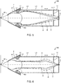
- FIG. 3 is a schematic cross-sectional view of the input lens, 300, associated with the third embodiment.
- Those members of the input lens 300 which are functionally similar to their counterparts of the input lens 100 associated with the first embodiment and the input lens 200 associated with the second embodiment are indicated by the same reference numerals as in the foregoing figures and a detailed description thereof is omitted.
- the distance between the ( n - 1)th electrode L n -1 and the optical axis O is less than both the distance between the ( n - 2)th electrode L n - 2 and the optical axis O and the distance between the n th electrode L n and the optical axis O.
- the ( n - 1)th electrode L n - 1 has a protrusive portion 4 protruding toward the optical axis O.
- FIG. 4 illustrates the operation of the input lens 300 and corresponds to FIG. 3 .
- the input lens 300 has two states of operation. In one of the two states, as shown in FIG. 3 , electrons are not focused within the input lens 300. In the other state, as shown in FIG. 4 , electrons are focused within the input lens 300.
- the ( n - 2)th electrode L n - 2, the ( n - 1)th electrode L n -1, and the n th electrode L n are substantially equipotential. These electrodes L n - 2 to L n together produce a weak lens action. Therefore, in the state of operation of FIG. 3 , the electron trajectory is almost identical to that shown in the state of operation of FIG. 2 , and electrons are focused at the slit S.
- electrons can be focused at two points, i.e., in the vicinity of the ( n - 1)th electrode L n -1 and at the slit S, as shown in FIG. 4 .
- the state of operation can be switched between the state of operation in which electrons are not focused within the input lens as shown in FIG. 3 and the state of operation in which electrons are focused within the input lens as shown in FIG. 4 , by controlling the voltages applied to the first through n th electrodes L1 to L n .
- the distance between the ( n - 1)th electrode L n -1 and the optical axis O is small and, therefore, a strong lens action can be produced in the vicinity of the ( n - 1)th electrode L n - 1. Consequently, electrons can be brought to a focus in the vicinity of the ( n - 1)th electrode L n -1.
- the image magnification factor of the input lens 300 and the set range of angular magnifications can be increased by varying the focal position.
- Good electron spectroscopy can be performed over a wider range of deceleration ratios by varying the image magnification or angular magnification according to the deceleration ratio. If electrons are focused within the input lens, there occurs the advantage that the image magnification and angular magnification can be set within wider ranges, but greater chromatic aberrations are produced. Accordingly, the state of operation is switched between the state of operation in which electrons are not focused within the input lens as shown in FIG. 3 and the state of operation in which electrons are focused within the input lens as shown in FIG. 4 according to electron spectroscopy conditions.
- the ( n - 1)th electrode L n - 1 is provided with the protrusive portion 4, and the distance between the ( n - 1)th electrode L n -1 and the optical axis O is less than both the distance between the ( n - 2)th electrode L n - 2 and the optical axis O and the distance between the n th electrode L n and the optical axis O.
- the distance between the m th electrode L m and the optical axis O may be less than both the distance between the ( m - 1)th electrode L m -1 and the optical axis O and the distance between the ( m + 1)th electrode L m + 1 and the optical axis O. As a result, a strong lens action can be produced in the vicinity of the m th electrode L m .
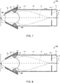
- FIGS. 5 and 6 illustrate the operation of the input lens 300.
- the input lens 300 can accomplish a spherical aberration correcting lens shown in FIG. 5 and an acceleration electrostatic lens shown in FIG. 6 .
- the input lens 300 shown in FIG. 5 When the input lens 300 shown in FIG. 5 is used as a spherical aberration correcting lens, the input lens 300 is operated similarly to the state of operation illustrated in FIG. 3 . That is, a positive voltage is applied to the second mesh M2 to thereby produce a convex lens in an accelerating field. The positive spherical aberration produced by the electric field set up between the reference electrode L0 and the second mesh M2 is reduced by the negative spherical aberration generated by the electric fields set up by the second to nth electrodes L2 to L n .
- FIG. 5 shows electron trajectories drawn under the conditions: electrons have energy Ek at the electron source P1 and energy Ep at the slit S and are accelerated by a factor of five in the input lens 300.
- Ep/Ek 5.00 ⁇ 0.95.
- Ep/Ek 5.00 ⁇ 1.00.
- Ep/Ek 5.00 ⁇ 1.05.
- spherical aberration can be reduced as shown in FIG. 5 .
- the potential difference between the first electrode L1 and the second electrode L2 of the input lens 300 is smaller than that in the input lens in the state of operation shown in FIG. 5 .
- FIG. 6 shows electron trajectories drawn under the conditions: electrons have energy Ek at the electron source P1 and energy Ep at the slit S and are accelerated by a factor of five in the input lens 300.
- Ep/Ek 5.00 ⁇ 0.95.
- Ep/Ek 5.00 ⁇ 1.00.
- Ep/Ek 5.00 ⁇ 1.05.
- chromatic aberration can be reduced as shown in FIG. 6 .
- electrons are accelerated by a factor of five in the input lens 300.
- the factor is merely exemplary and is not limited to five.
- the state of operation can be switched between the state of operation of FIG. 5 where the input lens 300 is operated as a spherical aberration correcting lens and the state of operation of FIG. 6 where the input lens 300 is operated as an acceleration electrostatic lens by controlling the voltages applied to the first through nth electrodes L1 to L n .
- the spherical aberration in the input lens is directly associated with the sensitivity of the electron analyzer, and the chromatic aberration in the input lens is directly associated with the range of energies of electrons that can be accepted at the same time. Consequently, the electron spectrometer including the input lens 300 can perform electron spectroscopy under optimum conditions by controlling the voltages applied to the first through nth electrodes L1 to L n according to electron spectroscopy conditions of the electron analyzer and other conditions.
- FIG. 7 is a schematic cross-sectional view of the input lens, 400, associated with the fourth embodiment.
- Those members of the input lens 400 which are similar in function to their respective counterparts of the input lens 100, input lens 200, and input lens 300 associated with the first, second, and third embodiments, respectively, are indicated by the same reference numerals as in the foregoing figures and a detailed description thereof is omitted.
- the input lens 400 includes a ground electrode Lg that is disposed outside the reference electrode L0.
- the ground electrode Lg is cylindrical, and the reference electrode L0 is disposed inside the ground electrode Lg.
- the reference electrode L0, the first electrode L1, and the second electrode L2 are arranged inside the ground electrode Lg that is at ground potential.
- the input lens 400 has a voltage source (not shown) for applying a voltage to the reference electrode L0.
- the reference potential is a positive potential. That is, positive voltages are applied to the reference electrode L0 and the first mesh M1. As a result, electrons can be efficiently guided from the electron source P1 to the first mesh M1. If voltage variations in the reference electrode L0 are made proportional to the energy being measured by the electron analyzer, the solid angle of acceptance subtended from the electron source P1 to the first mesh M1 is constant over the whole energy range.
- an objective lens is used as an electron source
- magnetic fields leaking out of the objective lens may reach close to the sample.
- the working distance between the bottom surface of the objective lens and the sample is short and the magnetic fields in the vicinities of the sample are higher.
- electrons emanating from the sample especially lower energy electrons, do not reach the first mesh M1 from the electron source P1 by the effects of the magnetic fields, thus lowering the sensitivity of the electron analyzer.
- the input lens 400 if a voltage of a positive fixed value is applied to the reference electrode L0, only lower energy electrons can be pulled into the first mesh M1. Therefore, deterioration of the sensitivity of the electron analyzer due to the objective lens magnetic field can be reduced. Furthermore, by increasing the voltage applied to the first mesh M1, the sensitivity to low energy electrons can be improved selectively.
- the linewidth of the electron beam is decreased in order to image or analyze microscopic regions.
- the prior-art input lens is used, secondary electrons released from the sample, backscattered electrons, and Auger electrons cannot enter the input lens due to magnetic fields leaking out of the objective lens. This may reduce the sensitivity of the electron analyzer. Especially, the sensitivity to lower energy electrons decreases.
- the input lens 400 As described above, lower energy electrons can be pulled into the first mesh M1 by applying a positive voltage to the reference electrode L0. Therefore, in an Auger electron spectrometer, if the objective lens is a semi-in lens or an in-lens, the sensitivity of the electron analyzer can be prevented from deteriorating.
- FIG. 8 is a schematic cross-sectional view of the input lens, 500, associated with the fifth embodiment.
- Those members of the input lens 500 which are similar in function to their counterparts of the input lens 100, input lens 200, input lens 300, and input lens 400, respectively, associated with the first, second, third, and fourth embodiments, are indicated by the same reference numerals as in the foregoing figures and a detailed description thereof is omitted.
- the input lens 500 does not have the first mesh M1.
- the sensitivity of the electron detector or analyzer can be enhanced as compared with the case where the first mesh M1 is attached.
- the sensitivity of the electron detector can be improved by an amount equal to "1 - transmissivity".
- the electric fields leaking out of the front end of the input lens 500 vary.
- the leaking electric fields can be adjusted, for example, with the voltage applied to the reference electrode L0.
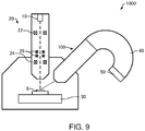
- FIG. 9 shows the configuration of the electron spectrometer, 1000, associated with the sixth embodiment.
- the electron spectrometer 1000 is an apparatus for analyzing a sample 6 by Auger electron spectroscopy.
- Auger electron spectroscopy is technology for performing elemental analysis by measuring the energies of Auger electrons emitted from a sample (e.g., sample 6) that are excited by an electron beam or the like and released from the sample.
- the electron spectrometer 1000 includes an electron source 10, an optical system 20, a sample stage 30, an input lens 100, an electron analyzer 40, and a detector 50.
- the electron source 10 produces an electron beam.
- the electron source 10 is an electron gun which emits an electron beam by accelerating electrons, released from a cathode, by means of an anode.
- the optical system 20 causes the electron beam emitted from the electron source 10 to be directed at the sample 6.
- the optical system 20 includes condenser lenses 22, an objective lens 24, and deflectors 26.
- the electron beam emitted from the electron source 10 can be focused into a probe of electrons by the condenser lenses 22 and the objective lens 24.
- the deflectors 26 deflect the electron beam focused by the condenser lenses 22 and the objective lens 24.
- the deflectors 26 are used, for example, to scan the electron beam over the sample 6.
- the sample stage 30 holds the sample 6 thereon.
- the sample stage 30 is equipped with a horizontal drive mechanism for moving the sample 6 horizontally, a vertical drive mechanism for moving the sample 6 in a heightwise direction, and a tilt mechanism for tilting the sample 6.
- the sample stage 30 permits the sample 6 to be placed in position.
- the electron analyzer 40 spectrally disperses Auger electrons produced from the sample 6 in response to irradiation of the sample 6 by the electron beam.
- the electron analyzer 40 is an electrostatic hemispherical analyzer, for example.
- the input lens 100 is positioned between the electron source and the electron analyzer 40, the electron source producing Auger electrons as the sample 6 is irradiated with the electron beam.
- the input lens 400 accepts incoming electrons and guides them into the electron analyzer 40.
- the input lens 100 provides variable energy resolution by decelerating the electrons. In the input lens 100, as electrons are decelerated to a greater extent, the resolution is improved but at the cost of the sensitivity.
- the electron analyzer 40 has an inner hemispherical electrode and an outer hemispherical electrode. In the electron analyzer 40, by applying a voltage between the inner and outer hemispherical electrodes, electrons having energies lying in an energy range corresponding to the applied voltage can be extracted. The detector 50 detects the electrons spectrally dispersed by the electron analyzer 40.
- the electron spectrometer 1000 includes the input lens 100 having a large acceptance solid angle ⁇ for electrons and, therefore, Auger electrons released from the sample can be detected at high sensitivity.
- the electron spectrometer 1000 includes the input lens 100.
- the electron spectrometer 1000 may include one of the above-described input lenses 200, 300, and 400.
- the electron spectrometer 1000 is an Auger electron spectrometer.
- the electron spectrometer 1000 may also be an X-ray photoelectron spectrometer or other type of electron spectrometer.
- the present invention is not restricted to the foregoing embodiments and that the invention can be practiced in variously varied forms.
- the invention embraces configurations which are substantially identical to the configurations described in the embodiments. What are meant by the substantially identical configurations are configurations which are identical in functions or method, for example.
- the present invention embraces configurations which are similar to the configurations described in the above embodiments except that nonessential portions have been replaced. Further, the present invention embraces configurations similar to the configurations of the above embodiments except that well-known techniques have been added.
Landscapes
- Chemical & Material Sciences (AREA)
- Analytical Chemistry (AREA)
- Analysing Materials By The Use Of Radiation (AREA)
- Electron Tubes For Measurement (AREA)
Applications Claiming Priority (1)
| Application Number | Priority Date | Filing Date | Title |
|---|---|---|---|
| JP2019178816A JP7030089B2 (ja) | 2019-09-30 | 2019-09-30 | インプットレンズおよび電子分光装置 |
Publications (1)
| Publication Number | Publication Date |
|---|---|
| EP3799108A1 true EP3799108A1 (fr) | 2021-03-31 |
Family
ID=72659758
Family Applications (1)
| Application Number | Title | Priority Date | Filing Date |
|---|---|---|---|
| EP20198606.4A Withdrawn EP3799108A1 (fr) | 2019-09-30 | 2020-09-28 | Lentille d'entrée et spectromètre d'électrons |
Country Status (3)
| Country | Link |
|---|---|
| US (1) | US11404260B2 (fr) |
| EP (1) | EP3799108A1 (fr) |
| JP (1) | JP7030089B2 (fr) |
Families Citing this family (1)
| Publication number | Priority date | Publication date | Assignee | Title |
|---|---|---|---|---|
| JP7105261B2 (ja) * | 2020-02-18 | 2022-07-22 | 日本電子株式会社 | オージェ電子分光装置および分析方法 |
Citations (4)
| Publication number | Priority date | Publication date | Assignee | Title |
|---|---|---|---|---|
| US5444242A (en) * | 1992-09-29 | 1995-08-22 | Physical Electronics Inc. | Scanning and high resolution electron spectroscopy and imaging |
| JPH08111199A (ja) * | 1994-10-12 | 1996-04-30 | Jeol Ltd | 球面収差補正静電型レンズ |
| US6104029A (en) * | 1997-08-26 | 2000-08-15 | Vg Systems Ltd. | Spectrometer and method of spectroscopy |
| JP4802340B2 (ja) | 2004-07-15 | 2011-10-26 | 国立大学法人 奈良先端科学技術大学院大学 | 球面収差補正静電型レンズ、インプットレンズ、電子分光装置、光電子顕微鏡、および測定システム |
Family Cites Families (14)
| Publication number | Priority date | Publication date | Assignee | Title |
|---|---|---|---|---|
| JPH04343054A (ja) * | 1991-05-20 | 1992-11-30 | Nippondenso Co Ltd | 光電子分光装置 |
| JPH0510897A (ja) * | 1991-07-02 | 1993-01-19 | Jeol Ltd | X線光電子分光イメージング装置 |
| US5315113A (en) | 1992-09-29 | 1994-05-24 | The Perkin-Elmer Corporation | Scanning and high resolution x-ray photoelectron spectroscopy and imaging |
| US5583336A (en) * | 1995-10-30 | 1996-12-10 | Kelly; Michael A. | High throughput electron energy analyzer |
| DE19929185A1 (de) * | 1999-06-25 | 2001-01-04 | Staib Instr Gmbh | Vorrichtung und Verfahren zur energie- und winkelaufgelösten Elektronenspektroskopie |
| JP4431698B2 (ja) | 2004-12-24 | 2010-03-17 | 独立行政法人産業技術総合研究所 | 飛行時間型分析装置 |
| EP2058834B1 (fr) * | 2006-07-26 | 2015-12-09 | National University Corporation Nara Institute of Science and Technology | Lentille à décélération à correction d'aberration sphérique, système de lentilles à correction d'aberration sphérique, dispositif de spectroscopie électronique, et microscope à photoélectrons |
| GB0700754D0 (en) | 2007-01-15 | 2007-02-21 | Oxford Instr Analytical Ltd | Charged particle analyser and method |
| WO2008114684A1 (fr) | 2007-03-16 | 2008-09-25 | National University Corporation NARA Institute of Science and Technology | Analyseur d'énergie, analyseur d'énergie de type à affichage bidimensionnel, et microscope photoélectronique |
| GB0720901D0 (en) * | 2007-10-24 | 2007-12-05 | Shimadzu Res Lab Europe Ltd | Charged particle energy analysers |
| US10586625B2 (en) * | 2012-05-14 | 2020-03-10 | Asml Netherlands B.V. | Vacuum chamber arrangement for charged particle beam generator |
| EP2997590B1 (fr) * | 2013-05-15 | 2018-01-10 | Okinawa Institute of Science and Technology School Corporation | Diffraction d'electrons de faible energie (leed) pour meb |
| WO2017010529A1 (fr) | 2015-07-15 | 2017-01-19 | 国立大学法人奈良先端科学技術大学院大学 | Lentille électrostatique, et dispositif de génération de faisceau parallèle et dispositif de convergence de faisceau parallèle utilisant la lentille électrostatique et un collimateur |
| CN109983386B (zh) * | 2016-11-21 | 2021-10-29 | 株式会社尼康 | 变倍光学系统、光学设备以及摄像设备 |
-
2019
- 2019-09-30 JP JP2019178816A patent/JP7030089B2/ja active Active
-
2020
- 2020-09-25 US US17/032,092 patent/US11404260B2/en active Active
- 2020-09-28 EP EP20198606.4A patent/EP3799108A1/fr not_active Withdrawn
Patent Citations (4)
| Publication number | Priority date | Publication date | Assignee | Title |
|---|---|---|---|---|
| US5444242A (en) * | 1992-09-29 | 1995-08-22 | Physical Electronics Inc. | Scanning and high resolution electron spectroscopy and imaging |
| JPH08111199A (ja) * | 1994-10-12 | 1996-04-30 | Jeol Ltd | 球面収差補正静電型レンズ |
| US6104029A (en) * | 1997-08-26 | 2000-08-15 | Vg Systems Ltd. | Spectrometer and method of spectroscopy |
| JP4802340B2 (ja) | 2004-07-15 | 2011-10-26 | 国立大学法人 奈良先端科学技術大学院大学 | 球面収差補正静電型レンズ、インプットレンズ、電子分光装置、光電子顕微鏡、および測定システム |
Also Published As
| Publication number | Publication date |
|---|---|
| JP7030089B2 (ja) | 2022-03-04 |
| JP2021057178A (ja) | 2021-04-08 |
| US11404260B2 (en) | 2022-08-02 |
| US20210098244A1 (en) | 2021-04-01 |
Similar Documents
| Publication | Publication Date | Title |
|---|---|---|
| EP1150327B1 (fr) | Dispositif multi-faisceaux de particules chargées | |
| US6043491A (en) | Scanning electron microscope | |
| JP6880209B2 (ja) | 走査電子顕微鏡 | |
| US8729466B1 (en) | Aberration-corrected and energy-filtered low energy electron microscope with monochromatic dual beam illumination | |
| US20240258067A1 (en) | Transmission charged particle microscope with an electron energy loss spectroscopy detector | |
| KR101815850B1 (ko) | 모노크로미터 및 이를 구비한 하전입자선 장치 | |
| CN110911259B (zh) | 具有改进的性能的多电子束成像设备 | |
| US20150340200A1 (en) | Electron beam imaging with dual wien-filter monochromator | |
| CN107301940A (zh) | 用于分析物体的方法以及执行该方法的带电粒子束装置 | |
| NL2012618A (en) | Scanning particle microscope having an energy selective detector system. | |
| US3617741A (en) | Electron spectroscopy system with a multiple electrode electron lens | |
| US6730907B1 (en) | Charged particle device | |
| US20040075053A1 (en) | Particle-optical arrangements and particle-optical systems | |
| US11404260B2 (en) | Input lens and electron spectrometer | |
| EP0537961B1 (fr) | Analyseurs en énergie de particules chargées | |
| US10446360B2 (en) | Particle source for producing a particle beam and particle-optical apparatus | |
| JPWO2016120971A1 (ja) | 荷電粒子線装置 | |
| US9543115B2 (en) | Electron microscope | |
| JP6104756B2 (ja) | 電子分光装置 | |
| EP3758042B1 (fr) | Monochromateur et système de faisceau de particules chargées | |
| US20230298845A1 (en) | Energy Filter, and Energy Analyzer and Charged Particle Beam Device Provided with Same | |
| US11276549B1 (en) | Compact arrangement for aberration correction of electron lenses | |
| KR20170113491A (ko) | 모노크로미터 및 이를 구비한 전자선 손실분광 장치 | |
| JP3814968B2 (ja) | 検査装置 | |
| JPH1027571A (ja) | トロイダル型分光器を有する分光装置 |
Legal Events
| Date | Code | Title | Description |
|---|---|---|---|
| PUAI | Public reference made under article 153(3) epc to a published international application that has entered the european phase |
Free format text: ORIGINAL CODE: 0009012 |
|
| STAA | Information on the status of an ep patent application or granted ep patent |
Free format text: STATUS: THE APPLICATION HAS BEEN PUBLISHED |
|
| AK | Designated contracting states |
Kind code of ref document: A1 Designated state(s): AL AT BE BG CH CY CZ DE DK EE ES FI FR GB GR HR HU IE IS IT LI LT LU LV MC MK MT NL NO PL PT RO RS SE SI SK SM TR |
|
| AX | Request for extension of the european patent |
Extension state: BA ME |
|
| STAA | Information on the status of an ep patent application or granted ep patent |
Free format text: STATUS: REQUEST FOR EXAMINATION WAS MADE |
|
| 17P | Request for examination filed |
Effective date: 20210910 |
|
| RBV | Designated contracting states (corrected) |
Designated state(s): AL AT BE BG CH CY CZ DE DK EE ES FI FR GB GR HR HU IE IS IT LI LT LU LV MC MK MT NL NO PL PT RO RS SE SI SK SM TR |
|
| STAA | Information on the status of an ep patent application or granted ep patent |
Free format text: STATUS: EXAMINATION IS IN PROGRESS |
|
| 17Q | First examination report despatched |
Effective date: 20230831 |
|
| STAA | Information on the status of an ep patent application or granted ep patent |
Free format text: STATUS: THE APPLICATION IS DEEMED TO BE WITHDRAWN |
|
| 18D | Application deemed to be withdrawn |
Effective date: 20250604 |