EP3807940B1 - Optoelektronische vorrichtung - Google Patents
Optoelektronische vorrichtung Download PDFInfo
- Publication number
- EP3807940B1 EP3807940B1 EP19746116.3A EP19746116A EP3807940B1 EP 3807940 B1 EP3807940 B1 EP 3807940B1 EP 19746116 A EP19746116 A EP 19746116A EP 3807940 B1 EP3807940 B1 EP 3807940B1
- Authority
- EP
- European Patent Office
- Prior art keywords
- conductive
- light
- emitting diodes
- wafer
- layers
- Prior art date
- Legal status (The legal status is an assumption and is not a legal conclusion. Google has not performed a legal analysis and makes no representation as to the accuracy of the status listed.)
- Active
Links
Images



Classifications
-
- H—ELECTRICITY
- H10—SEMICONDUCTOR DEVICES; ELECTRIC SOLID-STATE DEVICES NOT OTHERWISE PROVIDED FOR
- H10H—INORGANIC LIGHT-EMITTING SEMICONDUCTOR DEVICES HAVING POTENTIAL BARRIERS
- H10H20/00—Individual inorganic light-emitting semiconductor devices having potential barriers, e.g. light-emitting diodes [LED]
- H10H20/01—Manufacture or treatment
- H10H20/036—Manufacture or treatment of packages
- H10H20/0364—Manufacture or treatment of packages of interconnections
-
- H—ELECTRICITY
- H10—SEMICONDUCTOR DEVICES; ELECTRIC SOLID-STATE DEVICES NOT OTHERWISE PROVIDED FOR
- H10H—INORGANIC LIGHT-EMITTING SEMICONDUCTOR DEVICES HAVING POTENTIAL BARRIERS
- H10H20/00—Individual inorganic light-emitting semiconductor devices having potential barriers, e.g. light-emitting diodes [LED]
- H10H20/80—Constructional details
- H10H20/81—Bodies
- H10H20/813—Bodies having a plurality of light-emitting regions, e.g. multi-junction LEDs or light-emitting devices having photoluminescent regions within the bodies
-
- H—ELECTRICITY
- H10—SEMICONDUCTOR DEVICES; ELECTRIC SOLID-STATE DEVICES NOT OTHERWISE PROVIDED FOR
- H10H—INORGANIC LIGHT-EMITTING SEMICONDUCTOR DEVICES HAVING POTENTIAL BARRIERS
- H10H20/00—Individual inorganic light-emitting semiconductor devices having potential barriers, e.g. light-emitting diodes [LED]
- H10H20/80—Constructional details
- H10H20/81—Bodies
- H10H20/817—Bodies characterised by the crystal structures or orientations, e.g. polycrystalline, amorphous or porous
- H10H20/818—Bodies characterised by the crystal structures or orientations, e.g. polycrystalline, amorphous or porous within the light-emitting regions
-
- H—ELECTRICITY
- H10—SEMICONDUCTOR DEVICES; ELECTRIC SOLID-STATE DEVICES NOT OTHERWISE PROVIDED FOR
- H10H—INORGANIC LIGHT-EMITTING SEMICONDUCTOR DEVICES HAVING POTENTIAL BARRIERS
- H10H20/00—Individual inorganic light-emitting semiconductor devices having potential barriers, e.g. light-emitting diodes [LED]
- H10H20/80—Constructional details
- H10H20/81—Bodies
- H10H20/822—Materials of the light-emitting regions
- H10H20/824—Materials of the light-emitting regions comprising only Group III-V materials, e.g. GaP
- H10H20/825—Materials of the light-emitting regions comprising only Group III-V materials, e.g. GaP containing nitrogen, e.g. GaN
-
- H—ELECTRICITY
- H10—SEMICONDUCTOR DEVICES; ELECTRIC SOLID-STATE DEVICES NOT OTHERWISE PROVIDED FOR
- H10H—INORGANIC LIGHT-EMITTING SEMICONDUCTOR DEVICES HAVING POTENTIAL BARRIERS
- H10H20/00—Individual inorganic light-emitting semiconductor devices having potential barriers, e.g. light-emitting diodes [LED]
- H10H20/80—Constructional details
- H10H20/85—Packages
- H10H20/851—Wavelength conversion means
- H10H20/8514—Wavelength conversion means characterised by their shape, e.g. plate or foil
-
- H—ELECTRICITY
- H10—SEMICONDUCTOR DEVICES; ELECTRIC SOLID-STATE DEVICES NOT OTHERWISE PROVIDED FOR
- H10H—INORGANIC LIGHT-EMITTING SEMICONDUCTOR DEVICES HAVING POTENTIAL BARRIERS
- H10H20/00—Individual inorganic light-emitting semiconductor devices having potential barriers, e.g. light-emitting diodes [LED]
- H10H20/80—Constructional details
- H10H20/85—Packages
- H10H20/857—Interconnections, e.g. lead-frames, bond wires or solder balls
-
- H—ELECTRICITY
- H10—SEMICONDUCTOR DEVICES; ELECTRIC SOLID-STATE DEVICES NOT OTHERWISE PROVIDED FOR
- H10H—INORGANIC LIGHT-EMITTING SEMICONDUCTOR DEVICES HAVING POTENTIAL BARRIERS
- H10H29/00—Integrated devices, or assemblies of multiple devices, comprising at least one light-emitting semiconductor element covered by group H10H20/00
- H10H29/10—Integrated devices comprising at least one light-emitting semiconductor component covered by group H10H20/00
- H10H29/14—Integrated devices comprising at least one light-emitting semiconductor component covered by group H10H20/00 comprising multiple light-emitting semiconductor components
- H10H29/142—Two-dimensional arrangements, e.g. asymmetric LED layout
-
- H—ELECTRICITY
- H10—SEMICONDUCTOR DEVICES; ELECTRIC SOLID-STATE DEVICES NOT OTHERWISE PROVIDED FOR
- H10W—GENERIC PACKAGES, INTERCONNECTIONS, CONNECTORS OR OTHER CONSTRUCTIONAL DETAILS OF DEVICES COVERED BY CLASS H10
- H10W90/00—Package configurations
-
- H—ELECTRICITY
- H10—SEMICONDUCTOR DEVICES; ELECTRIC SOLID-STATE DEVICES NOT OTHERWISE PROVIDED FOR
- H10H—INORGANIC LIGHT-EMITTING SEMICONDUCTOR DEVICES HAVING POTENTIAL BARRIERS
- H10H20/00—Individual inorganic light-emitting semiconductor devices having potential barriers, e.g. light-emitting diodes [LED]
- H10H20/01—Manufacture or treatment
- H10H20/036—Manufacture or treatment of packages
- H10H20/0361—Manufacture or treatment of packages of wavelength conversion means
Definitions
- the present application relates to an optoelectronic device, in particular a display screen or an image projection device, comprising light-emitting diodes, based on semiconductor materials, and their manufacturing methods.
- a display pixel of an image corresponds to the unitary element of the image displayed by the optoelectronic device.
- the optoelectronic device is a color image display screen, it generally comprises, for the display of each display pixel of the image, at least three components, also called display sub-pixels, which each emit light radiation substantially in a single color (for example, red, green and blue). The superposition of the radiation emitted by these three display sub-pixels provides the observer with the colored sensation corresponding to the display pixel of the displayed image.
- the display pixel of the optoelectronic device is the set formed by the three display sub-pixels used for the display of a display pixel of an image.
- Each display sub-pixel can comprise a light source, in particular one or more light-emitting diodes, for example based on semiconductor materials.
- a known method of manufacturing a optoelectronic device, in particular a display screen or an image projection device, comprising light-emitting diodes, called the "pick and place” process consists in manufacturing the light-emitting diodes in the form of separate components, and in placing each light-emitting diode at a desired position on a support which may include conductive tracks for the electrical connection of the light-emitting diodes.
- a disadvantage of such a method is that it generally requires precise positioning of the light-emitting diodes on the support. This requires the implementation of alignment methods which are all the more complex as the dimensions of the light-emitting diodes are reduced.
- Another disadvantage of such a method is that an increase in the resolution of the optoelectronic device results in an increase in the number of transfers of light-emitting diodes on the support and therefore an increase in the duration of the manufacture of the optoelectronic device which may not not be compatible with manufacturing on an industrial scale.
- the LEDs For the realization of a large LED display screen composed of assembled unit LEDs, the LEDs must be assembled with driving circuits which control a number of LEDs.
- the assemblies comprising the control circuits and the light-emitting diodes are then interconnected by wires. This assembly reduces the amount of data that can be transmitted and it can be difficult to display a video stream.
- TFT Thin Film Transistor
- WO 2011/048318 A1 , FR 3 023 066 A1 and US 2017/358562 A1 disclose high resolution display screens of the prior art, integrating with a high density wired light emitting diodes on an active matrix.
- some of the conductive tracks interconnect electronic components of the first plate and conductive elements extend in the first insulating layers of the stack and are in contact with the first metal layer.
- each part of the first and second metal layers surrounded by a trench is connected to the first plate by one of the conductive elements.
- the first and second metal layers completely cover the first faces of the first and second plates.
- the method comprises a step of forming an electrode electrically connecting the second ends of all the light-emitting diodes.
- the insulated conductive trenches extend from the electrode to some of the conductive tracks.
- the insulated conductive trenches extend from the second face of the first plate as far as the electrode.
- the first and second metal layers are brought into contact before the formation of a photoluminescent layer covering the electrode.
- each trench is connected to one of the insulated conductor vias.
- the method comprises the formation of a second electrically insulating layer covering the light-emitting diodes, the second insulating layer being traversed by electrically conductive walls.
- each set of electronic components comprises a control circuit for the light-emitting diodes of the corresponding set of light-emitting diodes.
- the method comprises a step of thinning the second wafer before forming the second metal layer.
- the 3D light-emitting diodes are wire, conical or frustoconical diodes.
- the method comprises a step during which the first and second wafers are etched so as to form chips.
- some of the conductive tracks interconnect electronic components of the first plate and conductive elements included in the first insulating layers of the stack are in contact with the first metallic layer.
- each part of the first and second metal layers surrounded by a trench is connected to the first plate by one of the conductive elements.
- the first and second metal layers completely cover the first faces of the first and second plates.
- an electrode electrically connects the second ends of all light emitting diodes.
- the insulated conductive trenches extend from the electrode to a conductive track of the stack.
- the insulated conductive trenches extend from the second face of the first plate to the electrode.
- each trench is connected to one of the insulated conductive vias.
- a second electrically insulating layer covers the light-emitting diodes, the insulating layer being traversed by electrically conductive walls.
- the second metallic layer is in contact with the first ends of the light-emitting diodes.
- each set of electronic components comprises a control circuit for the light-emitting diodes of a corresponding set of light-emitting diodes.
- the 3D light-emitting diodes are wire, conical or frustoconical diodes.
- insulating and conductive are here considered to mean “electrically insulating” and “electrically conducting”.
- the present description relates to optoelectronic devices with three-dimensional or 3D elements, for example wire elements (microwires or nanowires), conical elements or frustoconical elements. More specifically, the devices described include wired light-emitting diodes. However, these embodiments can be implemented for three-dimensional elements other than wire diodes, for example three-dimensional elements in the shape of a pyramid.
- microwire designates a three-dimensional structure of elongated shape in a preferred direction, of which at least two dimensions, called minor dimensions, are between 5 nm and 2.5 ⁇ m, preferably between 50 nm and 2.5 ⁇ m, the third dimension, called major dimension, being at least equal to 1 time, preferably at least 5 times and even more preferably at least 10 times, the largest of the minor dimensions.
- the minor dimensions can be less than or equal to approximately 1 ⁇ m, preferably between 100 nm and 1 ⁇ m, more preferably between 100 nm and 300 nm.
- the height of each microwire or nanowire can be greater than or equal to 500 nm, preferably between 1 ⁇ m and 50 ⁇ m.
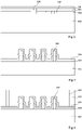
- the figure 1 represents part of an embodiment of an optoelectronic device 100, for example a display screen. More specifically, the figure 1 represents a display sub-pixel of a display pixel of the optoelectronic device 100.
- the display pixel comprises for example several display sub-pixels, for example at least three display sub-pixels.
- Such a display pixel comprises for example at least one display sub-pixel adapted to supply blue radiation, a display sub-pixel adapted to supply red radiation and a display sub-pixel adapted to supply a green radiation.
- the display pixel comprises an electronic circuit 101.
- Circuit 101 comprises a semiconductor substrate 102 in and on which sets of electronic components 103, represented very schematically in figure 1 , are formed. More precisely, each display sub-pixel comprises a set of electronic components 103.
- the substrate 102 is covered with a stack of at least one insulating layer, the stack further comprising conductive tracks 105 of a first level of metallization.
- the stack comprises two insulating layers 104 and 106.
- the conductive tracks 105 of the layer 104 serves for example to interconnect electronic components 103 of the same assembly.
- the display pixel further comprises an optoelectronic circuit 121.
- Circuit 121 comprises a semiconductor substrate 122 on which are formed sets of light-emitting diodes 120. More specifically, the display pixel comprises as many sets of light-emitting diodes than display sub-pixels, each display sub-pixel comprising a set of light-emitting diodes.
- Light-emitting diodes 120 are three-dimensional diodes as previously written. An example of light-emitting diodes 120 is described in the patent application US 2015/0255677 . A single set of light emitting diodes 120 is shown in figure 1 , this assembly comprising four light-emitting diodes. In practice, a set of light-emitting diodes can comprise between one and several tens of light-emitting diodes.
- Each set of electronic components 103 comprises for example a light-emitting diode control circuit. These sets of electronic components 103 are for example suitable for controlling a set of light-emitting diodes from the modulation of the voltage across the terminals of the sets of light-emitting diodes. Such circuits are described in the French patent application FR1756984 of the plaintiff.
- the electronic circuit 101 comprises a metallic layer 110, covering the insulating layer 106, and the optoelectronic circuit 121 comprises a metallic layer 142, covering the face of the substrate 122 opposite the light-emitting diodes 120.
- the metallic layers 110 and 142 are in contact with each other.
- the metal layers 110 and 142 are bonded by metal/metal molecular bonding and make it possible to fix the electronic circuit 101 to the optoelectronic circuit 121.
- the electronic circuit 101 comprises a conductive element 108, comprising for example conductive tracks located in the layers 104 and 106.
- the conductive element 108 makes it possible to form an electrical connection between each set of electronic components 103 and the metallic layer 110.
- conductive element 108 therefore makes it possible, for each set of electronic components 103, to form an electrical connection between the set of electronic components 103 of a display sub-pixel and the substrate 122 of the same display sub-pixel by the between the metal layers 110 and 142.
- the optoelectronic circuit 121 comprises an insulating layer 124 which covers the substrate 122 around the light-emitting diodes 120 and which covers a lower part of each light-emitting diode.
- the optoelectronic circuit 121 further comprises a conductive layer 126 which entirely covers the substrate 122, that is to say it covers the insulating layer 124 and the parts of the light-emitting diodes 120 not covered by the insulating layer 124.
- the conductive layer 126 is at least partially transparent to the radiation emitted by the light-emitting diodes.
- the conductive layer 126 corresponds to an electrode of the light-emitting diodes 120. This electrode is, preferably, an electrode common to all the light-emitting diodes 120 of the display sub-pixel.
- the optoelectronic circuit 121 comprises, for each display sub-pixel, a photoluminescent and insulating layer 130 covering the part of the conductive layer 126 associated with the display sub-pixel.
- the photoluminescent layer 130 is for example adapted to absorb at least part of the radiation emitted by the light-emitting diodes and to emit radiation at another wavelength.
- the photoluminescent layer 130 comprises for example quantum dots or phosphors.
- the composition of the photoluminescent layer 130 differs according to the display sub-pixel considered. Thus, certain photoluminescent layers 130 can be adapted to transform the radiation emitted by the light-emitting diodes of the display sub-pixel into blue, green or red radiation.
- substrate 122 may be absent.
- the metallic layer 142 is then directly in contact with the light-emitting diodes 120 and the insulating layer 124 or with a conductive nucleation layer allowing the latter to grow.
- Optoelectronic circuit 121 includes conductive walls 132 that extend from layer 126 to the face of photoluminescent layers 130 opposite substrate 122.
- walls 132 surround each set of light emitting diodes 120.
- the optoelectronic circuit 121 comprises a conductive layer 133 at least partially transparent to the radiation emitted by the display pixel, and covering the photoluminescent layers 130.
- the conductive layer 133 is for example in contact, and is for example electrically connected with the ends of the walls 132.
- the photoluminescent layer 130 can conformally cover the light-emitting diodes 120 and be covered with an insulating and transparent layer, for example of silicon.
- the electronic circuit 101 further comprises an insulating layer 150 located on the face of the substrate 102 opposite the insulating layers 104 and 106. 105.
- the insulated conductive vias 152 and 154 each comprise a conductive core 156 surrounded by an insulating sheath 158 open at the ends of the vias so as to allow electrical connection.
- the display pixel further includes isolated conductive trenches 160 located to surround each display sub-pixel.
- Each trench 160 comprises, like the vias 152 and 154, an insulating sheath 158 and a conductive core 156.
- the trenches 160 pass through the insulating layer 150, the substrate 102, the insulating layers 104 and 106, the metallic layers 110 and 142, the substrate 122 (if present), and the insulating layer 124.
- the trenches 160 delimit portions of the substrate 122 under each set of light-emitting diodes 120. The delimited portions are electrically isolated from the rest of the substrate 122.
- the layers 110 and 142 entirely cover, respectively, the faces of the electronic circuit 101 and of the optoelectronic circuit 121 on which they are formed, with the exception of the trenches 160.
- the electronic circuit 101 comprises a stack of insulating layers 162, further comprising conductive tracks, formed on the face of the insulating layer 150 opposite the substrate 102.
- conductive tracks 164 are formed so as to connect one end from one of the trenches 160 to one end of a via 154 of each display sub-pixel.
- the electronic circuit 101 comprises a metal layer 168 covering the face of the stack of layers 162 opposite to the insulating layer 150.
- the stack of layers 162 comprises conductive elements 166, comprising for example conductive tracks located in the layers 162. The conductive elements 166 make it possible to connect one end of at least one via 152 of each sub-pixel display to the metal layer 168.
- the display pixel is attached to a support 170 by metal/metal molecular bonding between the metal layer 168 and a metal layer forming a pad 172 located on the support 170.
- support 170 may not be covered with metallic layer 172 but with a stack of at least one insulating layer and first conductive tracks.
- the stack of layers 162 can comprise second conductive tracks facing the first conductive tracks. The first conductive tracks are located such that each first track is in contact with a second track.
- the insulating layers comprising the first and second tracks are thus bonded by hybrid molecular bonding.
- the electronic 101 and optoelectronic 121 circuits can be attached to each other similarly.
- a first supply potential for example a high potential, is applied to the conductive layer 133.
- This supply potential is therefore applied to a first end of the light-emitting diodes 120 via the walls 132 and the conductive layer 126.
- This supply potential is further provided to the electronic component assembly 103 of each display sub-pixel via trenches 160, conductive tracks 164, vias 154 and conductive tracks 105
- the sets of electronic components 103 are also connected to a second potential supply, for example a low potential, for example ground, via conductive tracks 105, vias 152, conductive elements 166, conductive layer 168, pads 172 and support 170.
- the set of electronic components 103 of each display sub-pixel provides, from these potentials, a control signal supplied to the second ends of the light-emitting diodes 120 through the intermediary of the conductive element 108, parts of the layers metal 110 and 142 surrounded by trenches 160 and substrate 122.
- the figures 2 to 8 illustrate the results of steps, preferably successive, of an embodiment of a method for manufacturing the optoelectronic device 100 of the figure 1 . More specifically, the figures 2 to 7 illustrate the manufacture of a display sub-pixel comprising an assembly of light-emitting diodes and an assembly of electronic components. The figure 8 illustrates the placement of display pixels.
- the substrates 102 and 122 can each correspond to a one-piece structure or correspond to a layer covering a support made of another material.
- the substrates 102 and 122 are preferably each a semiconductor substrate, for example a substrate made of silicon, germanium, silicon carbide, a III-V compound, or a II-VI compound, for example ZnO.
- Substrates 102 and 122 can also be sapphire or graphene.
- substrates 102 and 122 are single crystal silicon substrates.
- they are semiconductor substrates compatible with the manufacturing processes implemented in microelectronics.
- the substrates 102 and 122 may correspond to a multilayer structure of the silicon-on-insulator type, also called SOI (English acronym for Silicon On Insulator).
- Substrates 102 and 122 can be heavily doped, lightly doped, or undoped.
- group II chemical elements include group IIA chemical elements including beryllium (Be) and magnesium (Mg), and group IIB chemical elements including zinc (Zn), cadmium (Cd) and mercury (Hg).
- group VI chemical elements include group VIA chemical elements including oxygen (O) and tellurium (Te).
- compounds II-VI are ZnO, ZnMgO, CdZnO, CdZnMgO, CdHgTe, CdTe or HgTe. Generally speaking, the chemical elements in compound II-VI can be combined with different mole fractions.
- group III chemical elements include gallium (Ga), indium (In) or aluminum (Al).
- Group V chemical elements include nitrogen, phosphorus, or arsenic.
- III-N compounds are GaN, AlN, InN, InGaN, AlGaN or AlInGaN. Generally speaking, the chemical elements in the III-V compound can be combined with different mole fractions.
- the various insulating elements can be made of a dielectric material or comprise a stack of dielectric layers, for example of silicon oxide (SiO 2 ), of silicon nitride (Si x N y , where x is approximately equal to 3 and y is approximately equal to 4, for example Si 3 N 4 ), silicon oxynitride (in particular of general formula SiO x N y , for example Si 2 ON 2 ), hafnium oxide (HfO 2 ) or diamond.
- Conductive cores 156 are made of filler material.
- the filling material may correspond to a semiconductor or electrically conductive material.
- the conductive cores are, for example, made of silicon, germanium, silicon carbide, a III-V compound, such as GaN, InP or GaAs, a II-VI compound, for example ZnO, tungsten (W) or copper (Cu).
- each conductive core is made of polycrystalline silicon.
- each conductive core is made of a material compatible with the manufacturing methods used in microelectronics.
- Each conductive core can be heavily doped, lightly doped, or undoped.
- the picture 2 partially illustrates the formation of the electronic circuit 101 and more particularly the result of a step during which the sets of electronic components (not shown) are formed in and on the substrate 102.
- the substrate 102 corresponds to a plate (wafer) and is used for the simultaneous formation of electronic circuits 101.
- the stack of insulating layers 104 and 106 and the conductive tracks 105 are formed. Conductive elements 108 are also formed. Layer 106 is covered, over the whole of plate 102, by metallic layer 110.
- the picture 3 partially illustrates the formation of the optoelectronic circuit 121 and more specifically the result of a step during which the sets of light-emitting diodes 120 are formed on the substrate 122.
- a single set of light-emitting diodes 120 is represented in picture 3 , this assembly comprising four elementary light-emitting diodes.
- a set of light-emitting diodes can comprise between one and several hundred light-emitting diodes.
- the substrate 122 corresponds to a plate (wafer) and comprises a large number sets of light emitting diodes.
- the plate corresponding to the substrate 122 has substantially the same dimensions as the plate corresponding to the substrate 102 and the number of sets of light-emitting diodes 120 corresponds to the number of sets of electronic components 103.
- the insulating layer 124 and the conductive layer 126, forming the electrode, are formed on the whole of the plate of the substrate 102.
- the electrode 126 is, preferably, common to all the light-emitting diodes 120 of the plate.
- the figure 4 illustrates the result of another step in which conductive walls 132 are formed on conductive layer 126.
- Photoluminescent layer 130 is formed, for each display sub-pixel, in the location bounded by walls 132.
- the figure 5 illustrates another step in which a handle 140 is attached to the free face of the photoluminescent layers 130.
- Substrate 122 is then thinned.
- the metallic layer 142 is formed on the free face of the substrate 122, that is to say the face opposite the face on which the light-emitting diodes 120 are formed.
- the metallic layer 142 is formed on the whole of the plate.
- the handle 140 allows manipulation of the plate 122 without causing deformation in the plate during the thinning step and after this step.
- the metallic layer 142 covers, for example, the substrate 122 entirely.
- substrate 122 can be removed entirely.
- the metallic layer 142 is then formed directly in contact with the insulating layer 124 and one end of each light-emitting diode 120.
- the figure 6 illustrates another step in which the optoelectronic circuit board and the electronic circuit board are brought into contact with each other. More specifically, the metal layers 142 and 110 are brought into contact with each other. The two plates are therefore fixed by metal/metal molecular bonding.
- Each set of light-emitting diodes is located substantially opposite a set of electronic components 103 suitable for controlling this set of light-emitting diodes. There is thus an electrical connection, via substrate 122, layers 142 and 110 and conductive element 108, between one of the ends of each light-emitting diode 120 of a set of light-emitting diodes and the electronic components of the associated set of electronic components 103.
- the figure 7 illustrates the result of a step during which insulating layer 150 is deposited on the free face of substrate 102. Insulated conductive vias 152 and 154 are formed through insulating layer 150 and substrate 102 so as to achieve some of the conductive tracks.
- Isolated conductive trenches 160 are formed to surround each display sub-pixel. Trenches 160 pass through insulating layer 150, substrate 102, layers 104 and 106, metal layers 110 and 142, substrate 122 (if not completely removed), and insulating layer 124. The trenches 160 therefore connect the free face of the insulating layer 150 to the electrode 126.
- the insulating layers 162 and the conductive tracks 164 and 166 are formed on the free face of the insulating layer 150.
- the conductive tracks 164 are formed so as to connect one end of the trenches 160 to one end of a via 154 of each display sub-pixel.
- the conductive tracks 166 are formed so as to connect one end of the vias 152 to the free face of the layers 162.
- the layers 110 and 142 entirely cover the faces of the electronic 101 and optoelectronic 121 circuits on which they are formed before the formation of the trenches 160.
- the layers 110 and 142 preferably completely cover the faces of the electronic 101 and optoelectronic 121 circuits on which they are formed, with the exception of the trenches 160, which pass through them.
- the metal layer 168 is deposited on the free face of the stack of insulating layers 162. This layer 168 is therefore in contact with the conductive elements 166 and is therefore connected to a conductive track 105.
- the trenches 160 are therefore formed after the contacting of the optoelectronic circuit 121 and the electronic circuit 121.
- the figure 8 illustrates the result of a step during which trenches are dug between display pixels 169 so as to individualize them. Display pixels 169 nevertheless remain attached to handle 140.
- a certain number of display pixels 169 are deposited on the support 170.
- the metal pads 172 are formed at the desired locations of the display pixels 169.
- the handle 140 is then placed so as to put a display pixel opposite each metal stud 172.
- the gaps between the studs 172 are preferably chosen so that each display pixel 169 of a display screen can be placed, at the same time, next to the corresponding pad 172.
- the display pixels can be deposited several times.
- the display pixels 169 are then brought into contact with the studs 172 so as to fix by molecular bonding the pad 172 to the metallic layer 168, which is common to all the display sub-pixels of each display pixel 169.
- the handle 140 and the display pixels not having been joined to pads 172 are then removed.
- an insulating layer is deposited on the support 170 and on the display pixels in such a way that one end of each wall 132 of each display pixel 169 remains uncovered.
- the conductive layer 133 is then deposited on the insulating layer, in contact with the walls 132.
- the figure 9 illustrates part of another embodiment of an optoelectronic device 300. Specifically, the figure 9 illustrates a display sub-pixel of a display pixel of the optoelectronic device 300.
- the display sub-pixel of the figure 9 includes all of the sub-pixel elements of the figure 1 except that the trenches 160 of the embodiment of the figure 9 only pass through the insulating layer 106, the metal layers 110 and 142, the substrate 122 and the insulating layer 124.
- the assembly of electronic components 103 receives the first supply potential via the conductive layer 133, walls 132, trenches 160, and conductive tracks 105.
- the layers 110 and 142 entirely cover, respectively, the faces of the electronic circuit 101 and of the optoelectronic circuit 121 on which they are formed, with the exception of trenches 160.
- the figure 10 and 11 illustrate the results of steps, preferably successive, of an embodiment of a method for manufacturing the optoelectronic device 300 of the figure 9 .
- the figure 10 illustrates the result of steps comprising first steps similar to the steps described in connection with the figures 2 and 3 .
- Substrate 122 is then thinned. However, the thickness of the substrate 122 is kept sufficiently thick so that the manipulation of the substrate 122 does not require the use of a handle.
- the metal layer 142 is then deposited on the free face of the substrate 122. The metal layers 142 and 110 are then brought into contact so as to fix the electronic circuit board 101 and the optoelectronic circuit board 121 by molecular bonding as described previously.
- the figure 11 illustrates the result of steps during which the insulated conductive trenches 160 are formed, from the free face of the conductive layer 126.
- the trenches 160 comprise an electrically conductive core and an electrically insulating sheath.
- the sheaths are formed in such a way that the conductive core is in contact with the conductive layer 126 forming the electrode.
- the trenches 160 are formed so as to reach conductive tracks 105 in places.
- the trenches 160 are therefore formed after the contacting of the optoelectronic circuit 121 and the electronic circuit 121.
- Insulated conductive vias 152 are formed through substrate 102 so as to form a connection between the free face of substrate 102 and conductive tracks 105.
- the layers 110 and 142 entirely cover the faces of the electronic 101 and optoelectronic 121 circuits on which they are formed before the formation of the trenches 160.
- the layers 110 and 142 preferably entirely cover the faces of the electronic 101 and optoelectronic 121 circuits on which they are formed with the exception of the trenches 160, which pass through them.
- the conductive walls 132 are formed on the layer 126.
- the photoluminescent layer 130 of each sub-pixel is deposited on the light-emitting diodes of the sub-pixel concerned.
- the walls 132 are not in contact with the trenches 160.
- the walls 132 of the embodiments of the figure 1 and 9 may be formed directly in contact with one end of trenches 160.
- walls 132 may be in contact with conductive layer 126 and one end of trenches 160.
- a handle is also formed on the photoluminescent layers 130.
- the conductive layer 168 is formed on the free face of the substrate 102, connected to the vias 152.
- the display pixels are then individualized.
- the display pixels and the display sub-pixels are thus ready to be deposited on the support 170 so as to form a display screen, as described previously in relation to the figure 8 .
- Layer conductive 133 is then deposited on the display sub-pixels.
- the metal layers 142 and 110 can only partially cover the substrate 122 and the layer 106.
- the parts not covered by the layers 142 and 110 can be covered with another material, for example an insulating material.
- the optoelectronic circuit board and the electronic circuit board are then fixed by hybrid molecular bonding.
- the figure 12 illustrates part of another embodiment of an optoelectronic device 500. Specifically, the figure 12 illustrates a display sub-pixel of a display pixel of the optoelectronic device 500.
- the display sub-pixel of the embodiment shown at figure 12 does not include either conductive layer 133 covering insulating layer 130 or conductive walls 132 in photoluminescent layer 130.
- the trenches 160 cross, as in the embodiment of the figure 1 , the insulating layer 124, the substrate 122, the metal layers 142 and 110, the insulating layers 106 and 104, the substrate 102 and the insulating layer 150.
- the trenches 160 connect the electrode 126 to conductive tracks 180 located in the insulating layers 162.
- the layers 110 and 142 entirely cover, respectively, the faces of the electronic circuit 101 and of the optoelectronic circuit 121 on which they are formed, with the exception of the trenches 160.
- the support 170 is not covered with the metallic layer 172 but with a stack of at least one insulating layer 182 and conductive tracks 184.
- the tracks 184 are located in such a way that each track 180 is in contact with a track 184.
- Layers 182 and 162 are thus bonded by hybrid molecular bonding.
- layers 182 and 162 can be bonded in another way.
- Such other ways are described in the patents US 8898896 B2 and US 8586409 B2 .
- a voltage is applied to electrode 126 via tracks 184 and 180 and trenches 160, conductive tracks 184 being able for example to extend into insulating layer 182 as far as other pads not shown.
- Each set of electronic components is connected to voltage sources, for example to a supply voltage source and to ground, via conductive tracks 180 and 184, insulated conductive vias 152 and conductive tracks 105.
- the figures 13 and 14 illustrate the results of steps, preferably successive, of an embodiment of a manufacturing method of the optoelectronic device 500 of the figure 12 .
- the figure 13 illustrates the result of steps comprising first steps similar to the steps previously described in relation to the figures 2 and 3 .
- the insulating layer 130 is then deposited on the electrode 126 for each display sub-pixel. However, the walls 132 are not formed.
- a handle, not shown, is also attached to the photoluminescent layers 130, so as to be able to manipulate the optoelectronic circuit board.
- the metallic layer 142 is deposited on the free face of the substrate 122.
- the metallic layers 110 and 142 are fixed to each other by metal/metal molecular bonding. Alternatively, substrate 122 can be removed entirely.
- the figure 14 illustrates the result of steps during which insulated conductive vias 152 are formed from the free face of substrate 102 so as to reach conductive tracks 105.
- Insulating conductive trenches 160 are formed from the free face of substrate 102 and surround each display sub-pixel. The trenches 160 pass through the substrate 102, the layers 104 and 106, the metal layers 142 and 110, the substrate 122, and the insulating layer 124. Thus, the insulating trenches 160 form a connection between the free face of the substrate 102 and the electrode 126.
- the trenches 160 are therefore formed after the contacting of the optoelectronic circuit 121 and the electronic circuit 121.
- the layers 110 and 142 entirely cover the faces of the electronic 101 and optoelectronic 121 circuits on which they are formed before the formation of the trenches 160.
- the layers 110 and 142 preferably entirely cover the faces of the electronic 101 and optoelectronic 121 circuits on which they are formed with the exception of the trenches 160, which pass through them.
- the insulating layer 162 and the conductive tracks 180 are formed.
- the display pixels and the display sub-pixels are ready to be deposited on a chip so as to form a display screen.
- a step similar to the step described in connection with the figure 8 is carried out after the steps whose result is illustrated in figure 14 . It is not necessary to deposit a conductive layer on the layers photoluminescent 130 after removal of the handle. There are no conductive walls allowing the connection with the electrode 126.
- each display pixel is not deposited on a single pad, as described previously in relation to the figure 8 , but on the insulating layer 182 and the conductive tracks 184 so as to be able to separately connect the trenches 160 and the various vias 152.
- trenches 160 make it possible to isolate the parts of the layers 110 and 142 of each display sub-pixel and to individualize the connection of each set of light-emitting diodes.
- An advantage of the embodiments described previously is that the positioning, on the one hand of the substrate 122 on the substrate 102, and on the other hand of the display pixels 169 on the chips forming the display screen, is done by manipulating entire plates and not just individual elements. Thus, the process is faster than a process using a so-called “pick and place” technique.
- An advantage of the embodiments described previously is that, for each display sub-pixel, the connection between the set of light-emitting diodes and the set of associated electronic components 103 is made via layers 142 and 110. Thus, it is not necessary for the sets of light-emitting diodes and the sets of electronic components 103 to be perfectly aligned. This is also the case for the connection between the display pixels 169 and the pads 172 in the embodiments of the figure 1 and 9 .
Landscapes
- Led Device Packages (AREA)
- Devices For Indicating Variable Information By Combining Individual Elements (AREA)
- Led Devices (AREA)
Claims (20)
- Ein Verfahren zur Herstellung einer optoelektronischen Vorrichtung (100, 300, 500), das die folgenden Schritte aufweist:Ausbilden, auf einer ersten Oberfläche eines ersten Wafers (102), welche Anordnungen elektronischer Komponenten (103) aufweist, eines Stapels aus ersten Isolierschichten (104, 106) und Leiterbahnen (105);Ausbilden, auf einem zweiten Wafer (122), von Anordnungen dreidimensionaler Leuchtdioden (120), die jeweils ein erstes und ein zweites Ende aufweisen;Ausbilden einer ersten Metallschicht (110) auf mindestens einem Teil der ersten Oberfläche des ersten Wafers und einer zweiten Metallschicht (142) auf mindestens einem Teil einer ersten Oberfläche des zweiten Wafers, wobei die zweite Metallschicht elektrisch mit dem ersten Ende jeder Leuchtdiode (120) verbunden ist;In-Kontakt-Bringen der ersten und der zweiten Metallschicht (110, 142), um sie durch molekulares Bonden zu verbinden;Ausbilden mindestens einer isolierten leitenden Durchkontaktierung (152, 154), die eine zweite Oberfläche des ersten Wafers mit einer der Leiterbahnen (105) verbindet; undAusbilden, nach dem In-Kontakt-Bringen der ersten und der zweiten Metallschicht, von isolierten leitenden Gräben (160), die jede Anordnung von Leuchtdioden umgeben und Teile der ersten und zweiten Metallschicht (110, 142) seitlich voneinander isolieren, wobei jeder Teil mit einer der Anordnungen von Leuchtdioden verbunden ist.
- Verfahren nach Anspruch 1, wobei einige der Leiterbahnen (105) elektronische Komponenten des ersten Wafers miteinander verbinden und wobei sich leitende Elemente (108) in den ersten Isolierschichten des Stapels (104, 106) erstrecken und in Kontakt mit der ersten Metallschicht (110) stehen.
- Verfahren nach Anspruch 2, wobei jeder Teil der ersten und zweiten Metallschichten (110, 142), der von einem Graben (160) umgeben ist, durch eines der leitenden Elemente (108) mit dem ersten Wafer verbunden ist.
- Verfahren nach einem der Ansprüche 1 bis 3, wobei die ersten und zweiten Metallschichten (110, 142) vor dem Ausbilden von isolierten, leitenden Gräben (160) die ersten Oberflächen des ersten und des zweiten Wafers (102, 122) vollständig bedecken.
- Verfahren nach einem der Ansprüche 1 bis 4, wobei das Verfahren einen Schritt des Ausbildens einer Elektrode (126) aufweist, die die zweiten Enden aller Leuchtdioden (120) elektrisch verbindet.
- Verfahren nach Anspruch 5, wobei sich die isolierten, leitenden Gräben (160) von der Elektrode (126) zu einigen der Leiterbahnen (105) erstrecken.
- Verfahren nach Anspruch 5, wobei sich die isolierten, leitenden Gräben (160) von der zweiten Oberfläche des ersten Wafers zur Elektrode (126) erstrecken.
- Verfahren nach einem der Ansprüche 4 bis 7, wobei die erste und die zweite Metallschicht (110, 142) vor dem Ausbilden einer photolumineszierenden Schicht (130), die die Elektrode (126) bedeckt, in Kontakt gebracht werden.
- Verfahren nach einem der Ansprüche 1 bis 8, wobei jeder Graben (160) mit einer der isolierten leitenden Durchkontaktierungen (154) verbunden wird.
- Verfahren nach einem der Ansprüche 1 bis 9, aufweisend das Ausbilden einer zweiten elektrisch isolierende Schicht (130), die die lichtemittierenden Dioden abdeckt, wobei die zweite isolierende Schicht von elektrisch leitenden Wänden (132) gequert wird.
- Optoelektronisches Bauelement (100, 300, 500), das Folgendes aufweist:einen ersten Wafer mit Anordnungen elektronischer Komponenten und einem Stapel von ersten Isolierschichten (104, 106) und Leiterbahnen (105), wobei eine erste Oberfläche des ersten Wafers zumindest teilweise mit einer ersten Metallschicht (110) abgedeckt ist, wobei mindestens eine isolierte leitende Durchkontaktierung (154) eine zweite Oberfläche des ersten Wafers mit einer der Leiterbahnen verbindet;einen zweiten Wafer mit Anordnungen von dreidimensionalen lichtemittierenden Dioden (120), wobei jede lichtemittierende Diode ein erstes und ein zweites Ende aufweist, wobei eine erste Oberfläche des zweiten Wafers zumindest teilweise mit einer zweiten Metallschicht (142) abgedeckt ist, wobei die zweite Metallschicht elektrisch mit den ersten Enden aller lichtemittierenden Dioden gekoppelt ist, wobei die erste und die zweite Metallschicht (110, 142) durch molekulares Bonden miteinander verbunden sind; undisolierte, leitende Gräben (160), die jede Anordnung von Leuchtdioden umgeben, und Teile der ersten und zweiten Metallschicht, die mit jeder Anordnung von Leuchtdioden verbunden sind, seitlich isolieren.
- Vorrichtung nach Anspruch 11, wobei einige der Leiterbahnen (105) elektronische Komponenten des ersten Wafers miteinander verbinden und leitende Elemente (108), die in den ersten isolierenden Schichten des Stapels (104, 106) enthalten sind, in Kontakt mit der ersten Metallschicht (110) stehen.
- Vorrichtung nach Anspruch 12, wobei jeder Teil der ersten und zweiten Metallschichten (110, 142), der von einem Graben umgeben ist, mit dem ersten Wafer durch eines der leitenden Elemente (108) verbunden ist.
- Vorrichtung nach einem der Ansprüche 11 bis 13, wobei die ersten und zweiten Metallschichten (110, 142) die ersten Oberflächen des ersten und zweiten Wafers vollständig abdecken.
- Vorrichtung nach einem der Ansprüche 11 bis 14, wobei eine Elektrode (126) die zweiten Enden aller lichtemittierenden Dioden (120) elektrisch verbindet.
- Vorrichtung nach Anspruch 15, wobei sich die isolierten, leitenden Gräben (160) von der Elektrode (126) zu einer Leiterbahn des Stapels (104, 106) erstrecken.
- Vorrichtung nach Anspruch 15, wobei sich die isolierten, leitenden Gräben (160) von der zweiten Oberfläche des ersten Wafers zur Elektrode (126) erstrecken.
- Vorrichtung nach einem der Ansprüche 11 bis 17, wobei jeder Graben (160) mit einer der isolierten, leitenden Durchkontaktierungen (154) verbunden ist.
- Vorrichtung nach einem der Ansprüche 11 bis 18, wobei eine zweite elektrisch isolierender Schicht (130) die Leuchtdioden (120) abdeckt, wobei die isolierende Schicht von elektrisch leitenden Wänden (132) gequert wird.
- Vorrichtung nach einem der Ansprüche 11 bis 19, wobei die zweite Metallschicht (142) in Kontakt mit den ersten Enden der Leuchtdioden (120) steht.
Applications Claiming Priority (2)
| Application Number | Priority Date | Filing Date | Title |
|---|---|---|---|
| FR1870698A FR3082663B1 (fr) | 2018-06-14 | 2018-06-14 | Dispositif optoelectronique |
| PCT/FR2019/051410 WO2019239059A1 (fr) | 2018-06-14 | 2019-06-11 | Dispositif optoélectronique |
Publications (2)
| Publication Number | Publication Date |
|---|---|
| EP3807940A1 EP3807940A1 (de) | 2021-04-21 |
| EP3807940B1 true EP3807940B1 (de) | 2022-08-03 |
Family
ID=63491820
Family Applications (1)
| Application Number | Title | Priority Date | Filing Date |
|---|---|---|---|
| EP19746116.3A Active EP3807940B1 (de) | 2018-06-14 | 2019-06-11 | Optoelektronische vorrichtung |
Country Status (7)
| Country | Link |
|---|---|
| US (1) | US11581295B2 (de) |
| EP (1) | EP3807940B1 (de) |
| JP (1) | JP7313384B2 (de) |
| KR (1) | KR102744953B1 (de) |
| CN (1) | CN112470293B (de) |
| FR (1) | FR3082663B1 (de) |
| WO (1) | WO2019239059A1 (de) |
Citations (1)
| Publication number | Priority date | Publication date | Assignee | Title |
|---|---|---|---|---|
| EP3401958A1 (de) * | 2017-05-11 | 2018-11-14 | Commissariat à l'Energie Atomique et aux Energies Alternatives | Herstellungsverfahren einer led-emissionsanzeigevorrichtung |
Family Cites Families (18)
| Publication number | Priority date | Publication date | Assignee | Title |
|---|---|---|---|---|
| JPS62219954A (ja) * | 1986-03-20 | 1987-09-28 | Fujitsu Ltd | 三次元icの製造方法 |
| FR2876243B1 (fr) | 2004-10-04 | 2007-01-26 | Commissariat Energie Atomique | Composant a protuberances conductrices ductiles enterrees et procede de connexion electrique entre ce composant et un composant muni de pointes conductrices dures |
| US20070133356A1 (en) * | 2005-12-08 | 2007-06-14 | Zip Alarm Inc. | Alarm system with a plurality of interactive alarm units |
| FR2928033B1 (fr) | 2008-02-22 | 2010-07-30 | Commissariat Energie Atomique | Composant de connexion muni d'inserts creux. |
| FR2951875B1 (fr) * | 2009-10-23 | 2012-05-18 | Commissariat Energie Atomique | Procede de fabrication d?un ecran a tres haute resolution utilisant une couche conductrice anisotropique et emissive |
| JP5966412B2 (ja) | 2011-04-08 | 2016-08-10 | ソニー株式会社 | 画素チップ、表示パネル、照明パネル、表示装置および照明装置 |
| KR20140010521A (ko) | 2012-07-12 | 2014-01-27 | 삼성전자주식회사 | 발광소자 패키지 및 그 제조방법 |
| FR2997558B1 (fr) | 2012-10-26 | 2015-12-18 | Aledia | Dispositif opto-electrique et son procede de fabrication |
| FR3011388B1 (fr) * | 2013-09-30 | 2016-11-25 | Aledia | Dispositif optoelectronique a diodes electroluminescentes |
| FR3011381B1 (fr) * | 2013-09-30 | 2017-12-08 | Aledia | Dispositif optoelectronique a diodes electroluminescentes |
| DE102014100773A1 (de) | 2014-01-23 | 2015-07-23 | Osram Opto Semiconductors Gmbh | Halbleiterbauelement und Verfahren zur Herstellung eines Halbleiterbauelements |
| FR3023066B1 (fr) * | 2014-06-30 | 2017-10-27 | Aledia | Dispositif optoelectronique comprenant des diodes electroluminescentes et un circuit de commande |
| FR3031238B1 (fr) * | 2014-12-30 | 2016-12-30 | Aledia | Dispositif optoelectronique a diodes electroluminescentes |
| FR3033939B1 (fr) * | 2015-03-20 | 2018-04-27 | Commissariat A L'energie Atomique Et Aux Energies Alternatives | Dispositif optoelectronique a diode electroluminescente |
| DE102015108545A1 (de) | 2015-05-29 | 2016-12-01 | Osram Opto Semiconductors Gmbh | Optoelektronisches Bauelement und Verfahren zur Herstellung eines optoelektronischen Bauelements |
| US10177127B2 (en) | 2015-09-04 | 2019-01-08 | Hong Kong Beida Jade Bird Display Limited | Semiconductor apparatus and method of manufacturing the same |
| US10037981B2 (en) * | 2016-05-18 | 2018-07-31 | Globalfoundries Inc. | Integrated display system with multi-color light emitting diodes (LEDs) |
| FR3053530B1 (fr) | 2016-06-30 | 2018-07-27 | Aledia | Dispositif optoelectronique a pixels a contraste et luminance ameliores |
-
2018
- 2018-06-14 FR FR1870698A patent/FR3082663B1/fr not_active Expired - Fee Related
-
2019
- 2019-06-11 CN CN201980039921.XA patent/CN112470293B/zh active Active
- 2019-06-11 KR KR1020217001020A patent/KR102744953B1/ko active Active
- 2019-06-11 JP JP2020569812A patent/JP7313384B2/ja active Active
- 2019-06-11 US US17/251,762 patent/US11581295B2/en active Active
- 2019-06-11 EP EP19746116.3A patent/EP3807940B1/de active Active
- 2019-06-11 WO PCT/FR2019/051410 patent/WO2019239059A1/fr not_active Ceased
Patent Citations (1)
| Publication number | Priority date | Publication date | Assignee | Title |
|---|---|---|---|---|
| EP3401958A1 (de) * | 2017-05-11 | 2018-11-14 | Commissariat à l'Energie Atomique et aux Energies Alternatives | Herstellungsverfahren einer led-emissionsanzeigevorrichtung |
Also Published As
| Publication number | Publication date |
|---|---|
| KR20210020111A (ko) | 2021-02-23 |
| US20210134777A1 (en) | 2021-05-06 |
| JP7313384B2 (ja) | 2023-07-24 |
| FR3082663B1 (fr) | 2022-01-07 |
| EP3807940A1 (de) | 2021-04-21 |
| CN112470293A (zh) | 2021-03-09 |
| KR102744953B1 (ko) | 2024-12-19 |
| JP2021528846A (ja) | 2021-10-21 |
| US11581295B2 (en) | 2023-02-14 |
| FR3082663A1 (fr) | 2019-12-20 |
| WO2019239059A1 (fr) | 2019-12-19 |
| CN112470293B (zh) | 2024-05-03 |
Similar Documents
| Publication | Publication Date | Title |
|---|---|---|
| EP3401958B1 (de) | Herstellungsverfahren einer led-anzeigevorrichtung | |
| EP3455882B1 (de) | Verfahren zur herstellung einer optoelektronischen vorrichtung mit mehreren galliumnitriddioden | |
| US10629577B2 (en) | Direct-bonded LED arrays and applications | |
| EP3479408B1 (de) | Optoelektronische vorrichtung mit pixeln mit verbessertem kontrast und verbesserter helligkeit | |
| EP3410482B1 (de) | Optoelektronische vorrichtung mit leuchtdioden auf einem steuerschaltkreis | |
| EP3815139B1 (de) | Optoelektronische vorrichtung mit leuchtdioden | |
| EP3529834B1 (de) | Anzeigevorrichtung und verfahren zur herstellung solch einer vorrichtung | |
| EP3241245A1 (de) | Optoelektronische vorrichtung mit leuchtdioden | |
| EP3381060A1 (de) | Beleuchtete frontplatte und verfahren zur herstellung solch einer beleuchteten frontplatte | |
| JP2016502123A (ja) | 発光ダイオードディスプレイの製造方法および発光ダイオードディスプレイ | |
| WO2020128314A1 (fr) | Dispositif optoelectronique pour l'acquisition d'images selon plusieurs points de vue et/ou l'affichage d'images selon plusieurs points de vue | |
| EP3807940B1 (de) | Optoelektronische vorrichtung | |
| WO2021073981A1 (fr) | Procede de protection d'un dispositif optoelectronique contre les decharges electrostatiques | |
| EP4145507B1 (de) | Verfahren zur herstellung einer optoelektronischen vorrichtung und optoelektronische vorrichtung | |
| WO2022017972A1 (fr) | Dispositif optoelectronique flexible et son procede de fabrication | |
| WO2023126134A1 (fr) | Pixel d'affichage a diodes electroluminescentes pour ecran d'affichage |
Legal Events
| Date | Code | Title | Description |
|---|---|---|---|
| STAA | Information on the status of an ep patent application or granted ep patent |
Free format text: STATUS: UNKNOWN |
|
| STAA | Information on the status of an ep patent application or granted ep patent |
Free format text: STATUS: THE INTERNATIONAL PUBLICATION HAS BEEN MADE |
|
| PUAI | Public reference made under article 153(3) epc to a published international application that has entered the european phase |
Free format text: ORIGINAL CODE: 0009012 |
|
| STAA | Information on the status of an ep patent application or granted ep patent |
Free format text: STATUS: REQUEST FOR EXAMINATION WAS MADE |
|
| 17P | Request for examination filed |
Effective date: 20201125 |
|
| AK | Designated contracting states |
Kind code of ref document: A1 Designated state(s): AL AT BE BG CH CY CZ DE DK EE ES FI FR GB GR HR HU IE IS IT LI LT LU LV MC MK MT NL NO PL PT RO RS SE SI SK SM TR |
|
| AX | Request for extension of the european patent |
Extension state: BA ME |
|
| DAV | Request for validation of the european patent (deleted) | ||
| DAX | Request for extension of the european patent (deleted) | ||
| GRAP | Despatch of communication of intention to grant a patent |
Free format text: ORIGINAL CODE: EPIDOSNIGR1 |
|
| STAA | Information on the status of an ep patent application or granted ep patent |
Free format text: STATUS: GRANT OF PATENT IS INTENDED |
|
| INTG | Intention to grant announced |
Effective date: 20220223 |
|
| GRAS | Grant fee paid |
Free format text: ORIGINAL CODE: EPIDOSNIGR3 |
|
| GRAA | (expected) grant |
Free format text: ORIGINAL CODE: 0009210 |
|
| STAA | Information on the status of an ep patent application or granted ep patent |
Free format text: STATUS: THE PATENT HAS BEEN GRANTED |
|
| AK | Designated contracting states |
Kind code of ref document: B1 Designated state(s): AL AT BE BG CH CY CZ DE DK EE ES FI FR GB GR HR HU IE IS IT LI LT LU LV MC MK MT NL NO PL PT RO RS SE SI SK SM TR |
|
| REG | Reference to a national code |
Ref country code: AT Ref legal event code: REF Ref document number: 1509456 Country of ref document: AT Kind code of ref document: T Effective date: 20220815 Ref country code: CH Ref legal event code: EP |
|
| REG | Reference to a national code |
Ref country code: DE Ref legal event code: R096 Ref document number: 602019017854 Country of ref document: DE |
|
| REG | Reference to a national code |
Ref country code: IE Ref legal event code: FG4D Free format text: LANGUAGE OF EP DOCUMENT: FRENCH |
|
| REG | Reference to a national code |
Ref country code: LT Ref legal event code: MG9D |
|
| REG | Reference to a national code |
Ref country code: NL Ref legal event code: MP Effective date: 20220803 |
|
| PG25 | Lapsed in a contracting state [announced via postgrant information from national office to epo] |
Ref country code: SE Free format text: LAPSE BECAUSE OF FAILURE TO SUBMIT A TRANSLATION OF THE DESCRIPTION OR TO PAY THE FEE WITHIN THE PRESCRIBED TIME-LIMIT Effective date: 20220803 Ref country code: RS Free format text: LAPSE BECAUSE OF FAILURE TO SUBMIT A TRANSLATION OF THE DESCRIPTION OR TO PAY THE FEE WITHIN THE PRESCRIBED TIME-LIMIT Effective date: 20220803 Ref country code: PT Free format text: LAPSE BECAUSE OF FAILURE TO SUBMIT A TRANSLATION OF THE DESCRIPTION OR TO PAY THE FEE WITHIN THE PRESCRIBED TIME-LIMIT Effective date: 20221205 Ref country code: NO Free format text: LAPSE BECAUSE OF FAILURE TO SUBMIT A TRANSLATION OF THE DESCRIPTION OR TO PAY THE FEE WITHIN THE PRESCRIBED TIME-LIMIT Effective date: 20221103 Ref country code: NL Free format text: LAPSE BECAUSE OF FAILURE TO SUBMIT A TRANSLATION OF THE DESCRIPTION OR TO PAY THE FEE WITHIN THE PRESCRIBED TIME-LIMIT Effective date: 20220803 Ref country code: LV Free format text: LAPSE BECAUSE OF FAILURE TO SUBMIT A TRANSLATION OF THE DESCRIPTION OR TO PAY THE FEE WITHIN THE PRESCRIBED TIME-LIMIT Effective date: 20220803 Ref country code: LT Free format text: LAPSE BECAUSE OF FAILURE TO SUBMIT A TRANSLATION OF THE DESCRIPTION OR TO PAY THE FEE WITHIN THE PRESCRIBED TIME-LIMIT Effective date: 20220803 Ref country code: FI Free format text: LAPSE BECAUSE OF FAILURE TO SUBMIT A TRANSLATION OF THE DESCRIPTION OR TO PAY THE FEE WITHIN THE PRESCRIBED TIME-LIMIT Effective date: 20220803 Ref country code: ES Free format text: LAPSE BECAUSE OF FAILURE TO SUBMIT A TRANSLATION OF THE DESCRIPTION OR TO PAY THE FEE WITHIN THE PRESCRIBED TIME-LIMIT Effective date: 20220803 |
|
| REG | Reference to a national code |
Ref country code: AT Ref legal event code: MK05 Ref document number: 1509456 Country of ref document: AT Kind code of ref document: T Effective date: 20220803 |
|
| PG25 | Lapsed in a contracting state [announced via postgrant information from national office to epo] |
Ref country code: PL Free format text: LAPSE BECAUSE OF FAILURE TO SUBMIT A TRANSLATION OF THE DESCRIPTION OR TO PAY THE FEE WITHIN THE PRESCRIBED TIME-LIMIT Effective date: 20220803 Ref country code: IS Free format text: LAPSE BECAUSE OF FAILURE TO SUBMIT A TRANSLATION OF THE DESCRIPTION OR TO PAY THE FEE WITHIN THE PRESCRIBED TIME-LIMIT Effective date: 20221203 Ref country code: HR Free format text: LAPSE BECAUSE OF FAILURE TO SUBMIT A TRANSLATION OF THE DESCRIPTION OR TO PAY THE FEE WITHIN THE PRESCRIBED TIME-LIMIT Effective date: 20220803 Ref country code: GR Free format text: LAPSE BECAUSE OF FAILURE TO SUBMIT A TRANSLATION OF THE DESCRIPTION OR TO PAY THE FEE WITHIN THE PRESCRIBED TIME-LIMIT Effective date: 20221104 |
|
| PG25 | Lapsed in a contracting state [announced via postgrant information from national office to epo] |
Ref country code: SM Free format text: LAPSE BECAUSE OF FAILURE TO SUBMIT A TRANSLATION OF THE DESCRIPTION OR TO PAY THE FEE WITHIN THE PRESCRIBED TIME-LIMIT Effective date: 20220803 Ref country code: RO Free format text: LAPSE BECAUSE OF FAILURE TO SUBMIT A TRANSLATION OF THE DESCRIPTION OR TO PAY THE FEE WITHIN THE PRESCRIBED TIME-LIMIT Effective date: 20220803 Ref country code: DK Free format text: LAPSE BECAUSE OF FAILURE TO SUBMIT A TRANSLATION OF THE DESCRIPTION OR TO PAY THE FEE WITHIN THE PRESCRIBED TIME-LIMIT Effective date: 20220803 Ref country code: CZ Free format text: LAPSE BECAUSE OF FAILURE TO SUBMIT A TRANSLATION OF THE DESCRIPTION OR TO PAY THE FEE WITHIN THE PRESCRIBED TIME-LIMIT Effective date: 20220803 Ref country code: AT Free format text: LAPSE BECAUSE OF FAILURE TO SUBMIT A TRANSLATION OF THE DESCRIPTION OR TO PAY THE FEE WITHIN THE PRESCRIBED TIME-LIMIT Effective date: 20220803 |
|
| REG | Reference to a national code |
Ref country code: DE Ref legal event code: R097 Ref document number: 602019017854 Country of ref document: DE |
|
| PG25 | Lapsed in a contracting state [announced via postgrant information from national office to epo] |
Ref country code: SK Free format text: LAPSE BECAUSE OF FAILURE TO SUBMIT A TRANSLATION OF THE DESCRIPTION OR TO PAY THE FEE WITHIN THE PRESCRIBED TIME-LIMIT Effective date: 20220803 Ref country code: EE Free format text: LAPSE BECAUSE OF FAILURE TO SUBMIT A TRANSLATION OF THE DESCRIPTION OR TO PAY THE FEE WITHIN THE PRESCRIBED TIME-LIMIT Effective date: 20220803 |
|
| PLBE | No opposition filed within time limit |
Free format text: ORIGINAL CODE: 0009261 |
|
| STAA | Information on the status of an ep patent application or granted ep patent |
Free format text: STATUS: NO OPPOSITION FILED WITHIN TIME LIMIT |
|
| PG25 | Lapsed in a contracting state [announced via postgrant information from national office to epo] |
Ref country code: AL Free format text: LAPSE BECAUSE OF FAILURE TO SUBMIT A TRANSLATION OF THE DESCRIPTION OR TO PAY THE FEE WITHIN THE PRESCRIBED TIME-LIMIT Effective date: 20220803 |
|
| 26N | No opposition filed |
Effective date: 20230504 |
|
| PG25 | Lapsed in a contracting state [announced via postgrant information from national office to epo] |
Ref country code: SI Free format text: LAPSE BECAUSE OF FAILURE TO SUBMIT A TRANSLATION OF THE DESCRIPTION OR TO PAY THE FEE WITHIN THE PRESCRIBED TIME-LIMIT Effective date: 20220803 |
|
| PG25 | Lapsed in a contracting state [announced via postgrant information from national office to epo] |
Ref country code: MC Free format text: LAPSE BECAUSE OF FAILURE TO SUBMIT A TRANSLATION OF THE DESCRIPTION OR TO PAY THE FEE WITHIN THE PRESCRIBED TIME-LIMIT Effective date: 20220803 |
|
| PG25 | Lapsed in a contracting state [announced via postgrant information from national office to epo] |
Ref country code: MC Free format text: LAPSE BECAUSE OF FAILURE TO SUBMIT A TRANSLATION OF THE DESCRIPTION OR TO PAY THE FEE WITHIN THE PRESCRIBED TIME-LIMIT Effective date: 20220803 |
|
| REG | Reference to a national code |
Ref country code: CH Ref legal event code: PL |
|
| REG | Reference to a national code |
Ref country code: BE Ref legal event code: MM Effective date: 20230630 |
|
| PG25 | Lapsed in a contracting state [announced via postgrant information from national office to epo] |
Ref country code: LU Free format text: LAPSE BECAUSE OF NON-PAYMENT OF DUE FEES Effective date: 20230611 |
|
| REG | Reference to a national code |
Ref country code: IE Ref legal event code: MM4A |
|
| PG25 | Lapsed in a contracting state [announced via postgrant information from national office to epo] |
Ref country code: LU Free format text: LAPSE BECAUSE OF NON-PAYMENT OF DUE FEES Effective date: 20230611 |
|
| PG25 | Lapsed in a contracting state [announced via postgrant information from national office to epo] |
Ref country code: IE Free format text: LAPSE BECAUSE OF NON-PAYMENT OF DUE FEES Effective date: 20230611 |
|
| PG25 | Lapsed in a contracting state [announced via postgrant information from national office to epo] |
Ref country code: IE Free format text: LAPSE BECAUSE OF NON-PAYMENT OF DUE FEES Effective date: 20230611 Ref country code: CH Free format text: LAPSE BECAUSE OF NON-PAYMENT OF DUE FEES Effective date: 20230630 |
|
| PG25 | Lapsed in a contracting state [announced via postgrant information from national office to epo] |
Ref country code: IT Free format text: LAPSE BECAUSE OF FAILURE TO SUBMIT A TRANSLATION OF THE DESCRIPTION OR TO PAY THE FEE WITHIN THE PRESCRIBED TIME-LIMIT Effective date: 20220803 Ref country code: BE Free format text: LAPSE BECAUSE OF NON-PAYMENT OF DUE FEES Effective date: 20230630 |
|
| PG25 | Lapsed in a contracting state [announced via postgrant information from national office to epo] |
Ref country code: BG Free format text: LAPSE BECAUSE OF FAILURE TO SUBMIT A TRANSLATION OF THE DESCRIPTION OR TO PAY THE FEE WITHIN THE PRESCRIBED TIME-LIMIT Effective date: 20220803 |
|
| REG | Reference to a national code |
Ref country code: DE Ref legal event code: R079 Ref document number: 602019017854 Country of ref document: DE Free format text: PREVIOUS MAIN CLASS: H01L0033080000 Ipc: H10H0020813000 |
|
| PG25 | Lapsed in a contracting state [announced via postgrant information from national office to epo] |
Ref country code: BG Free format text: LAPSE BECAUSE OF FAILURE TO SUBMIT A TRANSLATION OF THE DESCRIPTION OR TO PAY THE FEE WITHIN THE PRESCRIBED TIME-LIMIT Effective date: 20220803 |
|
| PGFP | Annual fee paid to national office [announced via postgrant information from national office to epo] |
Ref country code: DE Payment date: 20250618 Year of fee payment: 7 |
|
| PGFP | Annual fee paid to national office [announced via postgrant information from national office to epo] |
Ref country code: GB Payment date: 20250618 Year of fee payment: 7 |
|
| PGFP | Annual fee paid to national office [announced via postgrant information from national office to epo] |
Ref country code: FR Payment date: 20250627 Year of fee payment: 7 |
|
| PG25 | Lapsed in a contracting state [announced via postgrant information from national office to epo] |
Ref country code: CY Free format text: LAPSE BECAUSE OF FAILURE TO SUBMIT A TRANSLATION OF THE DESCRIPTION OR TO PAY THE FEE WITHIN THE PRESCRIBED TIME-LIMIT; INVALID AB INITIO Effective date: 20190611 |
|
| PG25 | Lapsed in a contracting state [announced via postgrant information from national office to epo] |
Ref country code: HU Free format text: LAPSE BECAUSE OF FAILURE TO SUBMIT A TRANSLATION OF THE DESCRIPTION OR TO PAY THE FEE WITHIN THE PRESCRIBED TIME-LIMIT; INVALID AB INITIO Effective date: 20190611 |
|
| PG25 | Lapsed in a contracting state [announced via postgrant information from national office to epo] |
Ref country code: TR Free format text: LAPSE BECAUSE OF FAILURE TO SUBMIT A TRANSLATION OF THE DESCRIPTION OR TO PAY THE FEE WITHIN THE PRESCRIBED TIME-LIMIT Effective date: 20220803 |