EP3814680B1 - Optischer stapel für anzeige mit privatsphäre - Google Patents
Optischer stapel für anzeige mit privatsphäre Download PDFInfo
- Publication number
- EP3814680B1 EP3814680B1 EP19825030.0A EP19825030A EP3814680B1 EP 3814680 B1 EP3814680 B1 EP 3814680B1 EP 19825030 A EP19825030 A EP 19825030A EP 3814680 B1 EP3814680 B1 EP 3814680B1
- Authority
- EP
- European Patent Office
- Prior art keywords
- retarder
- retarders
- passive
- polariser
- liquid crystal
- Prior art date
- Legal status (The legal status is an assumption and is not a legal conclusion. Google has not performed a legal analysis and makes no representation as to the accuracy of the status listed.)
- Active
Links
Images

















Classifications
-
- G—PHYSICS
- G02—OPTICS
- G02F—OPTICAL DEVICES OR ARRANGEMENTS FOR THE CONTROL OF LIGHT BY MODIFICATION OF THE OPTICAL PROPERTIES OF THE MEDIA OF THE ELEMENTS INVOLVED THEREIN; NON-LINEAR OPTICS; FREQUENCY-CHANGING OF LIGHT; OPTICAL LOGIC ELEMENTS; OPTICAL ANALOGUE/DIGITAL CONVERTERS
- G02F1/00—Devices or arrangements for the control of the intensity, colour, phase, polarisation or direction of light arriving from an independent light source, e.g. switching, gating or modulating; Non-linear optics
- G02F1/01—Devices or arrangements for the control of the intensity, colour, phase, polarisation or direction of light arriving from an independent light source, e.g. switching, gating or modulating; Non-linear optics for the control of the intensity, phase, polarisation or colour
- G02F1/13—Devices or arrangements for the control of the intensity, colour, phase, polarisation or direction of light arriving from an independent light source, e.g. switching, gating or modulating; Non-linear optics for the control of the intensity, phase, polarisation or colour based on liquid crystals, e.g. single liquid crystal display cells
- G02F1/137—Devices or arrangements for the control of the intensity, colour, phase, polarisation or direction of light arriving from an independent light source, e.g. switching, gating or modulating; Non-linear optics for the control of the intensity, phase, polarisation or colour based on liquid crystals, e.g. single liquid crystal display cells characterised by the electro-optical or magneto-optical effect, e.g. field-induced phase transition, orientation effect, guest-host interaction or dynamic scattering
-
- G—PHYSICS
- G02—OPTICS
- G02B—OPTICAL ELEMENTS, SYSTEMS OR APPARATUS
- G02B6/00—Light guides; Structural details of arrangements comprising light guides and other optical elements, e.g. couplings
- G02B6/0001—Light guides; Structural details of arrangements comprising light guides and other optical elements, e.g. couplings specially adapted for lighting devices or systems
- G02B6/0011—Light guides; Structural details of arrangements comprising light guides and other optical elements, e.g. couplings specially adapted for lighting devices or systems the light guides being planar or of plate-like form
- G02B6/0033—Means for improving the coupling-out of light from the light guide
- G02B6/0035—Means for improving the coupling-out of light from the light guide provided on the surface of the light guide or in the bulk of it
- G02B6/0038—Linear indentations or grooves, e.g. arc-shaped grooves or meandering grooves, extending over the full length or width of the light guide
-
- G—PHYSICS
- G02—OPTICS
- G02B—OPTICAL ELEMENTS, SYSTEMS OR APPARATUS
- G02B6/00—Light guides; Structural details of arrangements comprising light guides and other optical elements, e.g. couplings
- G02B6/0001—Light guides; Structural details of arrangements comprising light guides and other optical elements, e.g. couplings specially adapted for lighting devices or systems
- G02B6/0011—Light guides; Structural details of arrangements comprising light guides and other optical elements, e.g. couplings specially adapted for lighting devices or systems the light guides being planar or of plate-like form
- G02B6/0033—Means for improving the coupling-out of light from the light guide
- G02B6/005—Means for improving the coupling-out of light from the light guide provided by one optical element, or plurality thereof, placed on the light output side of the light guide
- G02B6/0055—Reflecting element, sheet or layer
-
- G—PHYSICS
- G02—OPTICS
- G02F—OPTICAL DEVICES OR ARRANGEMENTS FOR THE CONTROL OF LIGHT BY MODIFICATION OF THE OPTICAL PROPERTIES OF THE MEDIA OF THE ELEMENTS INVOLVED THEREIN; NON-LINEAR OPTICS; FREQUENCY-CHANGING OF LIGHT; OPTICAL LOGIC ELEMENTS; OPTICAL ANALOGUE/DIGITAL CONVERTERS
- G02F1/00—Devices or arrangements for the control of the intensity, colour, phase, polarisation or direction of light arriving from an independent light source, e.g. switching, gating or modulating; Non-linear optics
- G02F1/01—Devices or arrangements for the control of the intensity, colour, phase, polarisation or direction of light arriving from an independent light source, e.g. switching, gating or modulating; Non-linear optics for the control of the intensity, phase, polarisation or colour
- G02F1/13—Devices or arrangements for the control of the intensity, colour, phase, polarisation or direction of light arriving from an independent light source, e.g. switching, gating or modulating; Non-linear optics for the control of the intensity, phase, polarisation or colour based on liquid crystals, e.g. single liquid crystal display cells
- G02F1/1323—Arrangements for providing a switchable viewing angle
-
- G—PHYSICS
- G02—OPTICS
- G02F—OPTICAL DEVICES OR ARRANGEMENTS FOR THE CONTROL OF LIGHT BY MODIFICATION OF THE OPTICAL PROPERTIES OF THE MEDIA OF THE ELEMENTS INVOLVED THEREIN; NON-LINEAR OPTICS; FREQUENCY-CHANGING OF LIGHT; OPTICAL LOGIC ELEMENTS; OPTICAL ANALOGUE/DIGITAL CONVERTERS
- G02F1/00—Devices or arrangements for the control of the intensity, colour, phase, polarisation or direction of light arriving from an independent light source, e.g. switching, gating or modulating; Non-linear optics
- G02F1/01—Devices or arrangements for the control of the intensity, colour, phase, polarisation or direction of light arriving from an independent light source, e.g. switching, gating or modulating; Non-linear optics for the control of the intensity, phase, polarisation or colour
- G02F1/13—Devices or arrangements for the control of the intensity, colour, phase, polarisation or direction of light arriving from an independent light source, e.g. switching, gating or modulating; Non-linear optics for the control of the intensity, phase, polarisation or colour based on liquid crystals, e.g. single liquid crystal display cells
- G02F1/133—Constructional arrangements; Operation of liquid crystal cells; Circuit arrangements
- G02F1/1333—Constructional arrangements; Manufacturing methods
- G02F1/13338—Input devices, e.g. touch panels
-
- G—PHYSICS
- G02—OPTICS
- G02F—OPTICAL DEVICES OR ARRANGEMENTS FOR THE CONTROL OF LIGHT BY MODIFICATION OF THE OPTICAL PROPERTIES OF THE MEDIA OF THE ELEMENTS INVOLVED THEREIN; NON-LINEAR OPTICS; FREQUENCY-CHANGING OF LIGHT; OPTICAL LOGIC ELEMENTS; OPTICAL ANALOGUE/DIGITAL CONVERTERS
- G02F1/00—Devices or arrangements for the control of the intensity, colour, phase, polarisation or direction of light arriving from an independent light source, e.g. switching, gating or modulating; Non-linear optics
- G02F1/01—Devices or arrangements for the control of the intensity, colour, phase, polarisation or direction of light arriving from an independent light source, e.g. switching, gating or modulating; Non-linear optics for the control of the intensity, phase, polarisation or colour
- G02F1/13—Devices or arrangements for the control of the intensity, colour, phase, polarisation or direction of light arriving from an independent light source, e.g. switching, gating or modulating; Non-linear optics for the control of the intensity, phase, polarisation or colour based on liquid crystals, e.g. single liquid crystal display cells
- G02F1/133—Constructional arrangements; Operation of liquid crystal cells; Circuit arrangements
- G02F1/1333—Constructional arrangements; Manufacturing methods
- G02F1/1335—Structural association of cells with optical devices, e.g. polarisers or reflectors
- G02F1/133504—Diffusing, scattering, diffracting elements
-
- G—PHYSICS
- G02—OPTICS
- G02F—OPTICAL DEVICES OR ARRANGEMENTS FOR THE CONTROL OF LIGHT BY MODIFICATION OF THE OPTICAL PROPERTIES OF THE MEDIA OF THE ELEMENTS INVOLVED THEREIN; NON-LINEAR OPTICS; FREQUENCY-CHANGING OF LIGHT; OPTICAL LOGIC ELEMENTS; OPTICAL ANALOGUE/DIGITAL CONVERTERS
- G02F1/00—Devices or arrangements for the control of the intensity, colour, phase, polarisation or direction of light arriving from an independent light source, e.g. switching, gating or modulating; Non-linear optics
- G02F1/01—Devices or arrangements for the control of the intensity, colour, phase, polarisation or direction of light arriving from an independent light source, e.g. switching, gating or modulating; Non-linear optics for the control of the intensity, phase, polarisation or colour
- G02F1/13—Devices or arrangements for the control of the intensity, colour, phase, polarisation or direction of light arriving from an independent light source, e.g. switching, gating or modulating; Non-linear optics for the control of the intensity, phase, polarisation or colour based on liquid crystals, e.g. single liquid crystal display cells
- G02F1/133—Constructional arrangements; Operation of liquid crystal cells; Circuit arrangements
- G02F1/1333—Constructional arrangements; Manufacturing methods
- G02F1/1335—Structural association of cells with optical devices, e.g. polarisers or reflectors
- G02F1/133528—Polarisers
-
- G—PHYSICS
- G02—OPTICS
- G02F—OPTICAL DEVICES OR ARRANGEMENTS FOR THE CONTROL OF LIGHT BY MODIFICATION OF THE OPTICAL PROPERTIES OF THE MEDIA OF THE ELEMENTS INVOLVED THEREIN; NON-LINEAR OPTICS; FREQUENCY-CHANGING OF LIGHT; OPTICAL LOGIC ELEMENTS; OPTICAL ANALOGUE/DIGITAL CONVERTERS
- G02F1/00—Devices or arrangements for the control of the intensity, colour, phase, polarisation or direction of light arriving from an independent light source, e.g. switching, gating or modulating; Non-linear optics
- G02F1/01—Devices or arrangements for the control of the intensity, colour, phase, polarisation or direction of light arriving from an independent light source, e.g. switching, gating or modulating; Non-linear optics for the control of the intensity, phase, polarisation or colour
- G02F1/13—Devices or arrangements for the control of the intensity, colour, phase, polarisation or direction of light arriving from an independent light source, e.g. switching, gating or modulating; Non-linear optics for the control of the intensity, phase, polarisation or colour based on liquid crystals, e.g. single liquid crystal display cells
- G02F1/133—Constructional arrangements; Operation of liquid crystal cells; Circuit arrangements
- G02F1/1333—Constructional arrangements; Manufacturing methods
- G02F1/1335—Structural association of cells with optical devices, e.g. polarisers or reflectors
- G02F1/133528—Polarisers
- G02F1/133536—Reflective polarizers
-
- G—PHYSICS
- G02—OPTICS
- G02F—OPTICAL DEVICES OR ARRANGEMENTS FOR THE CONTROL OF LIGHT BY MODIFICATION OF THE OPTICAL PROPERTIES OF THE MEDIA OF THE ELEMENTS INVOLVED THEREIN; NON-LINEAR OPTICS; FREQUENCY-CHANGING OF LIGHT; OPTICAL LOGIC ELEMENTS; OPTICAL ANALOGUE/DIGITAL CONVERTERS
- G02F1/00—Devices or arrangements for the control of the intensity, colour, phase, polarisation or direction of light arriving from an independent light source, e.g. switching, gating or modulating; Non-linear optics
- G02F1/01—Devices or arrangements for the control of the intensity, colour, phase, polarisation or direction of light arriving from an independent light source, e.g. switching, gating or modulating; Non-linear optics for the control of the intensity, phase, polarisation or colour
- G02F1/13—Devices or arrangements for the control of the intensity, colour, phase, polarisation or direction of light arriving from an independent light source, e.g. switching, gating or modulating; Non-linear optics for the control of the intensity, phase, polarisation or colour based on liquid crystals, e.g. single liquid crystal display cells
- G02F1/133—Constructional arrangements; Operation of liquid crystal cells; Circuit arrangements
- G02F1/1333—Constructional arrangements; Manufacturing methods
- G02F1/1335—Structural association of cells with optical devices, e.g. polarisers or reflectors
- G02F1/13363—Birefringent elements, e.g. for optical compensation
-
- G—PHYSICS
- G02—OPTICS
- G02F—OPTICAL DEVICES OR ARRANGEMENTS FOR THE CONTROL OF LIGHT BY MODIFICATION OF THE OPTICAL PROPERTIES OF THE MEDIA OF THE ELEMENTS INVOLVED THEREIN; NON-LINEAR OPTICS; FREQUENCY-CHANGING OF LIGHT; OPTICAL LOGIC ELEMENTS; OPTICAL ANALOGUE/DIGITAL CONVERTERS
- G02F1/00—Devices or arrangements for the control of the intensity, colour, phase, polarisation or direction of light arriving from an independent light source, e.g. switching, gating or modulating; Non-linear optics
- G02F1/01—Devices or arrangements for the control of the intensity, colour, phase, polarisation or direction of light arriving from an independent light source, e.g. switching, gating or modulating; Non-linear optics for the control of the intensity, phase, polarisation or colour
- G02F1/13—Devices or arrangements for the control of the intensity, colour, phase, polarisation or direction of light arriving from an independent light source, e.g. switching, gating or modulating; Non-linear optics for the control of the intensity, phase, polarisation or colour based on liquid crystals, e.g. single liquid crystal display cells
- G02F1/133—Constructional arrangements; Operation of liquid crystal cells; Circuit arrangements
- G02F1/1333—Constructional arrangements; Manufacturing methods
- G02F1/1335—Structural association of cells with optical devices, e.g. polarisers or reflectors
- G02F1/13363—Birefringent elements, e.g. for optical compensation
- G02F1/133634—Birefringent elements, e.g. for optical compensation the refractive index Nz perpendicular to the element surface being different from in-plane refractive indices Nx and Ny, e.g. biaxial or with normal optical axis
-
- G—PHYSICS
- G02—OPTICS
- G02F—OPTICAL DEVICES OR ARRANGEMENTS FOR THE CONTROL OF LIGHT BY MODIFICATION OF THE OPTICAL PROPERTIES OF THE MEDIA OF THE ELEMENTS INVOLVED THEREIN; NON-LINEAR OPTICS; FREQUENCY-CHANGING OF LIGHT; OPTICAL LOGIC ELEMENTS; OPTICAL ANALOGUE/DIGITAL CONVERTERS
- G02F1/00—Devices or arrangements for the control of the intensity, colour, phase, polarisation or direction of light arriving from an independent light source, e.g. switching, gating or modulating; Non-linear optics
- G02F1/01—Devices or arrangements for the control of the intensity, colour, phase, polarisation or direction of light arriving from an independent light source, e.g. switching, gating or modulating; Non-linear optics for the control of the intensity, phase, polarisation or colour
- G02F1/13—Devices or arrangements for the control of the intensity, colour, phase, polarisation or direction of light arriving from an independent light source, e.g. switching, gating or modulating; Non-linear optics for the control of the intensity, phase, polarisation or colour based on liquid crystals, e.g. single liquid crystal display cells
- G02F1/133—Constructional arrangements; Operation of liquid crystal cells; Circuit arrangements
- G02F1/1333—Constructional arrangements; Manufacturing methods
- G02F1/1335—Structural association of cells with optical devices, e.g. polarisers or reflectors
- G02F1/13363—Birefringent elements, e.g. for optical compensation
- G02F1/133638—Waveplates, i.e. plates with a retardation value of lambda/n
-
- G—PHYSICS
- G02—OPTICS
- G02F—OPTICAL DEVICES OR ARRANGEMENTS FOR THE CONTROL OF LIGHT BY MODIFICATION OF THE OPTICAL PROPERTIES OF THE MEDIA OF THE ELEMENTS INVOLVED THEREIN; NON-LINEAR OPTICS; FREQUENCY-CHANGING OF LIGHT; OPTICAL LOGIC ELEMENTS; OPTICAL ANALOGUE/DIGITAL CONVERTERS
- G02F1/00—Devices or arrangements for the control of the intensity, colour, phase, polarisation or direction of light arriving from an independent light source, e.g. switching, gating or modulating; Non-linear optics
- G02F1/01—Devices or arrangements for the control of the intensity, colour, phase, polarisation or direction of light arriving from an independent light source, e.g. switching, gating or modulating; Non-linear optics for the control of the intensity, phase, polarisation or colour
- G02F1/13—Devices or arrangements for the control of the intensity, colour, phase, polarisation or direction of light arriving from an independent light source, e.g. switching, gating or modulating; Non-linear optics for the control of the intensity, phase, polarisation or colour based on liquid crystals, e.g. single liquid crystal display cells
- G02F1/133—Constructional arrangements; Operation of liquid crystal cells; Circuit arrangements
- G02F1/1333—Constructional arrangements; Manufacturing methods
- G02F1/1337—Surface-induced orientation of the liquid crystal molecules, e.g. by alignment layers
-
- G—PHYSICS
- G02—OPTICS
- G02F—OPTICAL DEVICES OR ARRANGEMENTS FOR THE CONTROL OF LIGHT BY MODIFICATION OF THE OPTICAL PROPERTIES OF THE MEDIA OF THE ELEMENTS INVOLVED THEREIN; NON-LINEAR OPTICS; FREQUENCY-CHANGING OF LIGHT; OPTICAL LOGIC ELEMENTS; OPTICAL ANALOGUE/DIGITAL CONVERTERS
- G02F1/00—Devices or arrangements for the control of the intensity, colour, phase, polarisation or direction of light arriving from an independent light source, e.g. switching, gating or modulating; Non-linear optics
- G02F1/01—Devices or arrangements for the control of the intensity, colour, phase, polarisation or direction of light arriving from an independent light source, e.g. switching, gating or modulating; Non-linear optics for the control of the intensity, phase, polarisation or colour
- G02F1/13—Devices or arrangements for the control of the intensity, colour, phase, polarisation or direction of light arriving from an independent light source, e.g. switching, gating or modulating; Non-linear optics for the control of the intensity, phase, polarisation or colour based on liquid crystals, e.g. single liquid crystal display cells
- G02F1/133—Constructional arrangements; Operation of liquid crystal cells; Circuit arrangements
- G02F1/1333—Constructional arrangements; Manufacturing methods
- G02F1/1343—Electrodes
- G02F1/13439—Electrodes characterised by their electrical, optical, physical properties; materials therefor; method of making
-
- G—PHYSICS
- G02—OPTICS
- G02F—OPTICAL DEVICES OR ARRANGEMENTS FOR THE CONTROL OF LIGHT BY MODIFICATION OF THE OPTICAL PROPERTIES OF THE MEDIA OF THE ELEMENTS INVOLVED THEREIN; NON-LINEAR OPTICS; FREQUENCY-CHANGING OF LIGHT; OPTICAL LOGIC ELEMENTS; OPTICAL ANALOGUE/DIGITAL CONVERTERS
- G02F1/00—Devices or arrangements for the control of the intensity, colour, phase, polarisation or direction of light arriving from an independent light source, e.g. switching, gating or modulating; Non-linear optics
- G02F1/01—Devices or arrangements for the control of the intensity, colour, phase, polarisation or direction of light arriving from an independent light source, e.g. switching, gating or modulating; Non-linear optics for the control of the intensity, phase, polarisation or colour
- G02F1/13—Devices or arrangements for the control of the intensity, colour, phase, polarisation or direction of light arriving from an independent light source, e.g. switching, gating or modulating; Non-linear optics for the control of the intensity, phase, polarisation or colour based on liquid crystals, e.g. single liquid crystal display cells
- G02F1/137—Devices or arrangements for the control of the intensity, colour, phase, polarisation or direction of light arriving from an independent light source, e.g. switching, gating or modulating; Non-linear optics for the control of the intensity, phase, polarisation or colour based on liquid crystals, e.g. single liquid crystal display cells characterised by the electro-optical or magneto-optical effect, e.g. field-induced phase transition, orientation effect, guest-host interaction or dynamic scattering
- G02F1/139—Devices or arrangements for the control of the intensity, colour, phase, polarisation or direction of light arriving from an independent light source, e.g. switching, gating or modulating; Non-linear optics for the control of the intensity, phase, polarisation or colour based on liquid crystals, e.g. single liquid crystal display cells characterised by the electro-optical or magneto-optical effect, e.g. field-induced phase transition, orientation effect, guest-host interaction or dynamic scattering based on orientation effects in which the liquid crystal remains transparent
-
- G—PHYSICS
- G02—OPTICS
- G02F—OPTICAL DEVICES OR ARRANGEMENTS FOR THE CONTROL OF LIGHT BY MODIFICATION OF THE OPTICAL PROPERTIES OF THE MEDIA OF THE ELEMENTS INVOLVED THEREIN; NON-LINEAR OPTICS; FREQUENCY-CHANGING OF LIGHT; OPTICAL LOGIC ELEMENTS; OPTICAL ANALOGUE/DIGITAL CONVERTERS
- G02F1/00—Devices or arrangements for the control of the intensity, colour, phase, polarisation or direction of light arriving from an independent light source, e.g. switching, gating or modulating; Non-linear optics
- G02F1/01—Devices or arrangements for the control of the intensity, colour, phase, polarisation or direction of light arriving from an independent light source, e.g. switching, gating or modulating; Non-linear optics for the control of the intensity, phase, polarisation or colour
- G02F1/13—Devices or arrangements for the control of the intensity, colour, phase, polarisation or direction of light arriving from an independent light source, e.g. switching, gating or modulating; Non-linear optics for the control of the intensity, phase, polarisation or colour based on liquid crystals, e.g. single liquid crystal display cells
- G02F1/133—Constructional arrangements; Operation of liquid crystal cells; Circuit arrangements
- G02F1/1333—Constructional arrangements; Manufacturing methods
- G02F1/1335—Structural association of cells with optical devices, e.g. polarisers or reflectors
- G02F1/133528—Polarisers
- G02F1/133531—Polarisers characterised by the arrangement of polariser or analyser axes
-
- G—PHYSICS
- G02—OPTICS
- G02F—OPTICAL DEVICES OR ARRANGEMENTS FOR THE CONTROL OF LIGHT BY MODIFICATION OF THE OPTICAL PROPERTIES OF THE MEDIA OF THE ELEMENTS INVOLVED THEREIN; NON-LINEAR OPTICS; FREQUENCY-CHANGING OF LIGHT; OPTICAL LOGIC ELEMENTS; OPTICAL ANALOGUE/DIGITAL CONVERTERS
- G02F1/00—Devices or arrangements for the control of the intensity, colour, phase, polarisation or direction of light arriving from an independent light source, e.g. switching, gating or modulating; Non-linear optics
- G02F1/01—Devices or arrangements for the control of the intensity, colour, phase, polarisation or direction of light arriving from an independent light source, e.g. switching, gating or modulating; Non-linear optics for the control of the intensity, phase, polarisation or colour
- G02F1/13—Devices or arrangements for the control of the intensity, colour, phase, polarisation or direction of light arriving from an independent light source, e.g. switching, gating or modulating; Non-linear optics for the control of the intensity, phase, polarisation or colour based on liquid crystals, e.g. single liquid crystal display cells
- G02F1/133—Constructional arrangements; Operation of liquid crystal cells; Circuit arrangements
- G02F1/1333—Constructional arrangements; Manufacturing methods
- G02F1/1337—Surface-induced orientation of the liquid crystal molecules, e.g. by alignment layers
- G02F1/133738—Surface-induced orientation of the liquid crystal molecules, e.g. by alignment layers for homogeneous alignment
-
- G—PHYSICS
- G02—OPTICS
- G02F—OPTICAL DEVICES OR ARRANGEMENTS FOR THE CONTROL OF LIGHT BY MODIFICATION OF THE OPTICAL PROPERTIES OF THE MEDIA OF THE ELEMENTS INVOLVED THEREIN; NON-LINEAR OPTICS; FREQUENCY-CHANGING OF LIGHT; OPTICAL LOGIC ELEMENTS; OPTICAL ANALOGUE/DIGITAL CONVERTERS
- G02F1/00—Devices or arrangements for the control of the intensity, colour, phase, polarisation or direction of light arriving from an independent light source, e.g. switching, gating or modulating; Non-linear optics
- G02F1/01—Devices or arrangements for the control of the intensity, colour, phase, polarisation or direction of light arriving from an independent light source, e.g. switching, gating or modulating; Non-linear optics for the control of the intensity, phase, polarisation or colour
- G02F1/13—Devices or arrangements for the control of the intensity, colour, phase, polarisation or direction of light arriving from an independent light source, e.g. switching, gating or modulating; Non-linear optics for the control of the intensity, phase, polarisation or colour based on liquid crystals, e.g. single liquid crystal display cells
- G02F1/133—Constructional arrangements; Operation of liquid crystal cells; Circuit arrangements
- G02F1/1333—Constructional arrangements; Manufacturing methods
- G02F1/1337—Surface-induced orientation of the liquid crystal molecules, e.g. by alignment layers
- G02F1/133742—Surface-induced orientation of the liquid crystal molecules, e.g. by alignment layers for homeotropic alignment
-
- G—PHYSICS
- G02—OPTICS
- G02F—OPTICAL DEVICES OR ARRANGEMENTS FOR THE CONTROL OF LIGHT BY MODIFICATION OF THE OPTICAL PROPERTIES OF THE MEDIA OF THE ELEMENTS INVOLVED THEREIN; NON-LINEAR OPTICS; FREQUENCY-CHANGING OF LIGHT; OPTICAL LOGIC ELEMENTS; OPTICAL ANALOGUE/DIGITAL CONVERTERS
- G02F1/00—Devices or arrangements for the control of the intensity, colour, phase, polarisation or direction of light arriving from an independent light source, e.g. switching, gating or modulating; Non-linear optics
- G02F1/01—Devices or arrangements for the control of the intensity, colour, phase, polarisation or direction of light arriving from an independent light source, e.g. switching, gating or modulating; Non-linear optics for the control of the intensity, phase, polarisation or colour
- G02F1/13—Devices or arrangements for the control of the intensity, colour, phase, polarisation or direction of light arriving from an independent light source, e.g. switching, gating or modulating; Non-linear optics for the control of the intensity, phase, polarisation or colour based on liquid crystals, e.g. single liquid crystal display cells
- G02F1/137—Devices or arrangements for the control of the intensity, colour, phase, polarisation or direction of light arriving from an independent light source, e.g. switching, gating or modulating; Non-linear optics for the control of the intensity, phase, polarisation or colour based on liquid crystals, e.g. single liquid crystal display cells characterised by the electro-optical or magneto-optical effect, e.g. field-induced phase transition, orientation effect, guest-host interaction or dynamic scattering
- G02F1/13706—Devices or arrangements for the control of the intensity, colour, phase, polarisation or direction of light arriving from an independent light source, e.g. switching, gating or modulating; Non-linear optics for the control of the intensity, phase, polarisation or colour based on liquid crystals, e.g. single liquid crystal display cells characterised by the electro-optical or magneto-optical effect, e.g. field-induced phase transition, orientation effect, guest-host interaction or dynamic scattering the liquid crystal having positive dielectric anisotropy
-
- G—PHYSICS
- G02—OPTICS
- G02F—OPTICAL DEVICES OR ARRANGEMENTS FOR THE CONTROL OF LIGHT BY MODIFICATION OF THE OPTICAL PROPERTIES OF THE MEDIA OF THE ELEMENTS INVOLVED THEREIN; NON-LINEAR OPTICS; FREQUENCY-CHANGING OF LIGHT; OPTICAL LOGIC ELEMENTS; OPTICAL ANALOGUE/DIGITAL CONVERTERS
- G02F1/00—Devices or arrangements for the control of the intensity, colour, phase, polarisation or direction of light arriving from an independent light source, e.g. switching, gating or modulating; Non-linear optics
- G02F1/01—Devices or arrangements for the control of the intensity, colour, phase, polarisation or direction of light arriving from an independent light source, e.g. switching, gating or modulating; Non-linear optics for the control of the intensity, phase, polarisation or colour
- G02F1/13—Devices or arrangements for the control of the intensity, colour, phase, polarisation or direction of light arriving from an independent light source, e.g. switching, gating or modulating; Non-linear optics for the control of the intensity, phase, polarisation or colour based on liquid crystals, e.g. single liquid crystal display cells
- G02F1/137—Devices or arrangements for the control of the intensity, colour, phase, polarisation or direction of light arriving from an independent light source, e.g. switching, gating or modulating; Non-linear optics for the control of the intensity, phase, polarisation or colour based on liquid crystals, e.g. single liquid crystal display cells characterised by the electro-optical or magneto-optical effect, e.g. field-induced phase transition, orientation effect, guest-host interaction or dynamic scattering
- G02F1/13712—Devices or arrangements for the control of the intensity, colour, phase, polarisation or direction of light arriving from an independent light source, e.g. switching, gating or modulating; Non-linear optics for the control of the intensity, phase, polarisation or colour based on liquid crystals, e.g. single liquid crystal display cells characterised by the electro-optical or magneto-optical effect, e.g. field-induced phase transition, orientation effect, guest-host interaction or dynamic scattering the liquid crystal having negative dielectric anisotropy
-
- G—PHYSICS
- G02—OPTICS
- G02F—OPTICAL DEVICES OR ARRANGEMENTS FOR THE CONTROL OF LIGHT BY MODIFICATION OF THE OPTICAL PROPERTIES OF THE MEDIA OF THE ELEMENTS INVOLVED THEREIN; NON-LINEAR OPTICS; FREQUENCY-CHANGING OF LIGHT; OPTICAL LOGIC ELEMENTS; OPTICAL ANALOGUE/DIGITAL CONVERTERS
- G02F1/00—Devices or arrangements for the control of the intensity, colour, phase, polarisation or direction of light arriving from an independent light source, e.g. switching, gating or modulating; Non-linear optics
- G02F1/01—Devices or arrangements for the control of the intensity, colour, phase, polarisation or direction of light arriving from an independent light source, e.g. switching, gating or modulating; Non-linear optics for the control of the intensity, phase, polarisation or colour
- G02F1/13—Devices or arrangements for the control of the intensity, colour, phase, polarisation or direction of light arriving from an independent light source, e.g. switching, gating or modulating; Non-linear optics for the control of the intensity, phase, polarisation or colour based on liquid crystals, e.g. single liquid crystal display cells
- G02F1/137—Devices or arrangements for the control of the intensity, colour, phase, polarisation or direction of light arriving from an independent light source, e.g. switching, gating or modulating; Non-linear optics for the control of the intensity, phase, polarisation or colour based on liquid crystals, e.g. single liquid crystal display cells characterised by the electro-optical or magneto-optical effect, e.g. field-induced phase transition, orientation effect, guest-host interaction or dynamic scattering
- G02F1/13725—Devices or arrangements for the control of the intensity, colour, phase, polarisation or direction of light arriving from an independent light source, e.g. switching, gating or modulating; Non-linear optics for the control of the intensity, phase, polarisation or colour based on liquid crystals, e.g. single liquid crystal display cells characterised by the electro-optical or magneto-optical effect, e.g. field-induced phase transition, orientation effect, guest-host interaction or dynamic scattering based on guest-host interaction
-
- G—PHYSICS
- G02—OPTICS
- G02F—OPTICAL DEVICES OR ARRANGEMENTS FOR THE CONTROL OF LIGHT BY MODIFICATION OF THE OPTICAL PROPERTIES OF THE MEDIA OF THE ELEMENTS INVOLVED THEREIN; NON-LINEAR OPTICS; FREQUENCY-CHANGING OF LIGHT; OPTICAL LOGIC ELEMENTS; OPTICAL ANALOGUE/DIGITAL CONVERTERS
- G02F1/00—Devices or arrangements for the control of the intensity, colour, phase, polarisation or direction of light arriving from an independent light source, e.g. switching, gating or modulating; Non-linear optics
- G02F1/01—Devices or arrangements for the control of the intensity, colour, phase, polarisation or direction of light arriving from an independent light source, e.g. switching, gating or modulating; Non-linear optics for the control of the intensity, phase, polarisation or colour
- G02F1/13—Devices or arrangements for the control of the intensity, colour, phase, polarisation or direction of light arriving from an independent light source, e.g. switching, gating or modulating; Non-linear optics for the control of the intensity, phase, polarisation or colour based on liquid crystals, e.g. single liquid crystal display cells
- G02F1/137—Devices or arrangements for the control of the intensity, colour, phase, polarisation or direction of light arriving from an independent light source, e.g. switching, gating or modulating; Non-linear optics for the control of the intensity, phase, polarisation or colour based on liquid crystals, e.g. single liquid crystal display cells characterised by the electro-optical or magneto-optical effect, e.g. field-induced phase transition, orientation effect, guest-host interaction or dynamic scattering
- G02F1/13775—Polymer-stabilized liquid crystal layers
-
- G—PHYSICS
- G02—OPTICS
- G02F—OPTICAL DEVICES OR ARRANGEMENTS FOR THE CONTROL OF LIGHT BY MODIFICATION OF THE OPTICAL PROPERTIES OF THE MEDIA OF THE ELEMENTS INVOLVED THEREIN; NON-LINEAR OPTICS; FREQUENCY-CHANGING OF LIGHT; OPTICAL LOGIC ELEMENTS; OPTICAL ANALOGUE/DIGITAL CONVERTERS
- G02F2203/00—Function characteristic
- G02F2203/62—Switchable arrangements whereby the element being usually not switchable
-
- G—PHYSICS
- G02—OPTICS
- G02F—OPTICAL DEVICES OR ARRANGEMENTS FOR THE CONTROL OF LIGHT BY MODIFICATION OF THE OPTICAL PROPERTIES OF THE MEDIA OF THE ELEMENTS INVOLVED THEREIN; NON-LINEAR OPTICS; FREQUENCY-CHANGING OF LIGHT; OPTICAL LOGIC ELEMENTS; OPTICAL ANALOGUE/DIGITAL CONVERTERS
- G02F2413/00—Indexing scheme related to G02F1/13363, i.e. to birefringent elements, e.g. for optical compensation, characterised by the number, position, orientation or value of the compensation plates
- G02F2413/14—Negative birefingence
-
- G—PHYSICS
- G06—COMPUTING OR CALCULATING; COUNTING
- G06F—ELECTRIC DIGITAL DATA PROCESSING
- G06F3/00—Input arrangements for transferring data to be processed into a form capable of being handled by the computer; Output arrangements for transferring data from processing unit to output unit, e.g. interface arrangements
- G06F3/01—Input arrangements or combined input and output arrangements for interaction between user and computer
- G06F3/03—Arrangements for converting the position or the displacement of a member into a coded form
- G06F3/041—Digitisers, e.g. for touch screens or touch pads, characterised by the transducing means
- G06F3/044—Digitisers, e.g. for touch screens or touch pads, characterised by the transducing means by capacitive means
- G06F3/0445—Digitisers, e.g. for touch screens or touch pads, characterised by the transducing means by capacitive means using two or more layers of sensing electrodes, e.g. using two layers of electrodes separated by a dielectric layer
Definitions
- This disclosure generally relates to optical stacks for use in privacy display and low stray light displays.
- Privacy displays provide image visibility to a primary user that is typically in an on-axis position and reduced visibility of image content to a snooper, that is typically in an off-axis position.
- a privacy function may be provided by micro-louvre optical films that transmit a high luminance from a display in an on-axis direction with low luminance in off-axis positions, however such films are not switchable, and thus the display is limited to privacy only function.
- US 2010/0149459 A1 discloses an example of a privacy display device comprising: a liquid crystal panel; a display polariser arranged on the output side of the liquid crystal panel, the display polariser being a linear polariser; an additional polariser arranged on the output side of display polariser, the additional polariser being a linear polariser; and plural polar direction control retarders arranged between the additional polariser and the display polariser, wherein the plural polar direction control retarders are passive retarders, which together are capable of simultaneously introducing no net, relative phase shift to orthogonal polarisation components of light passed by the display polariser along an axis along a normal to the plane of the plural polar direction control retarders and introducing a net, relative phase shift to orthogonal polarisation components of light passed by the display polariser along an axis inclined to a normal to the plane of the plural polar direction control retarders.
- US 6,392,727 B1 discloses a display device with a display panel having an image of
- Switchable privacy displays may be provided by control of the off-axis optical output.
- Control of off-axis privacy may be provided by means of contrast reduction, for example by adjusting the liquid crystal bias tilt in an In-Plane-Switching LCD.
- Control may be further provided by means of off-axis luminance reduction.
- Luminance reduction may be achieved by means of switchable backlights for a liquid crystal display (LCD) spatial light modulator.
- Off-axis luminance reduction may also be provided by switchable liquid crystal retarders and compensation retarders arranged to modulate the input and/or output directional luminance profile of a spatial light modulator.
- Control may be further provided by means of off-axis reflectivity increase.
- Reflectivity increase may be achieved by means of switchable liquid crystal retarders, and compensation retarders that are arranged to control the polarisation of ambient light that falls onto a reflective polariser.
- a display device comprising: a spatial light modulator; a display polariser arranged on the output side of the spatial light modulator, the display polariser being a linear polariser; an additional polariser arranged on the output side of display polariser, the additional polariser being a linear polariser; and plural polar direction control retarders arranged between the additional polariser and the display polariser, wherein the plural polar direction control retarders include at least one passive retarder and together are capable of simultaneously introducing no net, relative phase shift to orthogonal polarisation components of light passed by the display polariser along an axis along a normal to the plane of the plural polar direction control retarders and introducing a net, relative phase shift to orthogonal polarisation components of light passed by the display polariser along an axis inclined to a normal to the plane of the plural polar direction control retarders, and wherein an air gap divides the plural polar direction control retarders into at least one air gap input retard
- a privacy display may be provided to achieve high luminance to an on-axis user and low luminance to an off-axis snooper, achieving high visual security level.
- An air gap is arranged to achieve reduced assembly cost and improve manufacturing yield.
- Multiple spatial light modulators may be arranged with a single retardation stack and additional polariser.
- Image contrast may be optimised for the head-on user.
- the plural polar direction control retarders may include at least one passive retarder.
- the cost of the display may be reduced.
- the polar angular range over which high visual security level is achieved may be increased in comparison to displays without passive retarders.
- the plural polar direction control retarders may further comprise two passive retarders which have optical axes in the plane of the retarders that are crossed, the two passive retarders being respectively included in the at least one air gap output retarder and the at least one air gap input retarder, the two passive retarders introducing no net, relative phase shift to orthogonal polarisation components of light passed by the display polariser along an axis along a normal to the plane of the plural polar direction control retarders, and the one of the two passive retarders which is arranged in the at least one air gap retarder being arranged to convert linearly polarised light passed by the display polariser into circularly polarised light.
- the retardance of the at least one passive compensation retarder may be equal and opposite to the retardance of the switchable liquid crystal retarder.
- the plural polar direction control retarders may include a switchable liquid crystal retarder comprising a layer of liquid crystal material.
- the switchable liquid crystal retarder may comprise two surface alignment layers disposed adjacent to the layer of liquid crystal material and on opposite sides thereof, each of the surface alignment layers being arranged to provide homeotropic alignment in the adjacent liquid crystal material.
- the layer of liquid crystal material of the switchable liquid crystal retarder may comprise a liquid crystal material with a negative dielectric anisotropy.
- the layer of liquid crystal material may have a retardance for light of a wavelength of 550nm in a range from 500nm to 1000nm, preferably in a range from 600nm to 900nm and most preferably in a range from 700nm to 850nm.
- the plural polar direction control retarders may further include: a passive retarder which has an optical axis perpendicular to the plane of the retarder, the passive retarder having a retardance for light of a wavelength of 550nm in a range from -300nm to -900nm, preferably in a range from -450nm to -800nm and most preferably in a range from -500nm to -725nm; or a pair of passive retarders which have optical axes in the plane of the retarders that are crossed, each retarder of the pair of passive retarders having a retardance for light of a wavelength of 550nm in a range from 300nm to 800nm, preferably in a range from 500nm to 700nm and most preferably in a range from 550nm to 675nm.
- the public mode may be provided with low power consumption.
- the passive retarders may be provided to match the liquid crystal mode.
- the switchable liquid crystal retarder may comprise two surface alignment layers disposed adjacent to the layer of liquid crystal material and on opposite sides thereof, each of the surface alignment layers being arranged to provide homogeneous alignment in the adjacent liquid crystal material.
- the layer of liquid crystal material of the switchable liquid crystal retarder may comprise a liquid crystal material with a positive dielectric anisotropy.
- the layer of liquid crystal material may have a retardance for light of a wavelength of 550nm in a range from 500nm to 1000nm, preferably in a range from 600nm to 850nm and most preferably in a range from 700nm to 800nm.
- the plural polar direction control retarders may further include: a passive retarder which has an optical axis perpendicular to the plane of the retarder, the retarder having a retardance for light of a wavelength of 550nm in a range from -300nm to -700nm, preferably in a range from -350nm to -600nm and most preferably in a range from -400nm to -500nm; or a pair of passive retarders which have optical axes in the plane of the retarders that are crossed, each retarder of the pair of passive retarders having a retardance for light of a wavelength of 550nm in a range from 300nm to 800nm, preferably in a range from 350nm to 650nm and most preferably in a range from 450nm to 550nm.
- the display may have increased resilience to applied mechanical stress.
- Each alignment layer may have a pretilt having a pretilt direction with a component in the plane of the liquid crystal layer that is parallel or anti-parallel or orthogonal to the electric vector transmission direction of the display polariser.
- the switchable liquid crystal retarder may further comprise electrodes arranged to apply a voltage for controlling the layer of liquid crystal material. The electrodes may be on opposite sides of the layer of liquid crystal material.
- the display polariser and the additional polariser may have electric vector transmission directions that are parallel.
- the display may be controlled to switch between privacy and public modes with high efficiency.
- the display polariser and the additional polariser may have electric vector transmission directions that are not parallel, and the display device may further comprise a rotator retarder arranged between the additional polariser and the display polariser, the rotator retarder being arranged to rotate a polarisation direction of polarised light incident thereon between the electric vector transmission directions of the display polariser and the additional polariser.
- the spatial light modulator may include a layer of twisted nematic liquid crystal material.
- a reflective polariser is arranged between the display polariser and additional polariser, the reflective polariser being a linear polariser.
- the display polariser and the reflective polariser may have electric vector transmission directions that are parallel.
- Advantageously off-axis visual security level of the display may be increased for reduced ambient light levels in comparison to displays without the reflective polariser.
- a diffusing surface structure may be provided on at least one of the at least one air gap input retarder and at least one air gap output retarder.
- Advantageously specular reflections at interfaces may be reduced.
- the display device may further comprise at least one further retarder and a further additional polariser, wherein the at least one further retarder is arranged between the first-mentioned additional polariser and the further additional polariser.
- the off-axis luminance may be further reduced in privacy mode in comparison to displays comprising a single additional polariser.
- Desirable visual security levels may be achieved using wide angle luminance output profiles from the spatial light modulator. Wide angle backlights may be used that may be manufactured with higher yields in comparison to collimated backlights. Emissive displays may be provided with switchable privacy functionality while achieving high visual security levels.
- the display device may further comprise a backlight arranged to output light, wherein the spatial light modulator is a transmissive spatial light modulator arranged to receive output light from the backlight.
- the backlight may provide a luminance at polar angles to the normal to the spatial light modulator greater than 45 degrees that is at most 33% of the luminance along the normal to the spatial light modulator, preferably at most 20% of the luminance along the normal to the spatial light modulator, and most preferably at most 10% of the luminance along the normal to the spatial light modulator.
- a further additional polariser may not be provided in order to achieve desirable visual security levels for off-axis snoopers. Display thickness, complexity and cost may be reduced.
- the backlight may comprise: an array of light sources; a directional waveguide comprising: an input end extending in a lateral direction along a side of the directional waveguide, the light sources being disposed along the input end and arranged to input input light into the waveguide; and opposed first and second guide surfaces extending across the directional waveguide from the input end for guiding light input at the input end along the waveguide, the waveguide being arranged to deflect input light guided through the directional waveguide to exit through the first guide surface.
- the backlight may further comprise a light turning film and the directional waveguide is a collimating waveguide.
- the collimating waveguide may comprise: (i) a plurality of elongate lenticular elements; and (ii) a plurality of inclined light extraction features, wherein the plurality of elongate lenticular elements and the plurality of inclined light extraction features are oriented to deflect input light guided through the directional waveguide to exit through the first guide surface.
- the directional waveguide may be an imaging waveguide arranged to image the light sources in the lateral direction so that the output light from the light sources is directed into respective optical windows in output directions that are distributed in dependence on the input positions of the light sources.
- the imaging waveguide may comprise a reflective end for reflecting the input light back along the imaging waveguide, wherein the second guide surface is arranged to deflect the reflected input light through the first guide surface as output light, the second guide surface comprises light extraction features and intermediate regions between the light extraction features, the light extraction features being oriented to deflect the reflected input light through the first guide surface as output light and the intermediate regions being arranged to direct light through the waveguide without extracting it; and the reflective end has positive optical power in the lateral direction extending between sides of the waveguide that extend between the first and second guide surfaces.
- the display device may further comprise an input polariser arranged on the input side of the spatial light modulator.
- Advantageously low cost collimating backlights with low thickness may be provided.
- the display device may further comprise a further additional polariser arranged on the input side of the spatial light modulator and at least one further retarder arranged between the at least one further additional polariser and the input polariser.
- a further additional polariser arranged on the input side of the spatial light modulator and at least one further retarder arranged between the at least one further additional polariser and the input polariser.
- the thickness added to the front of the display may be reduced.
- No air gap input and output retarders may be provided for the at least one further retarder.
- the complexity of the retarder stack may be reduced, reducing thickness and cost.
- the spatial light modulator may comprise an emissive spatial light modulator.
- Advantageously device thickness may be reduced.
- Embodiments of the present disclosure may be used in a variety of optical systems.
- the embodiment may include or work with a variety of projectors, projection systems, optical components, displays, microdisplays, computer systems, processors, self-contained projector systems, visual and/or audio-visual systems and electrical and/or optical devices.
- aspects of the present disclosure may be used with practically any apparatus related to optical and electrical devices, optical systems, presentation systems or any apparatus that may contain any type of optical system. Accordingly, embodiments of the present disclosure may be employed in optical systems, devices used in visual and/or optical presentations, visual peripherals and so on and in a number of computing environments.
- Directional backlights offer control over the illumination emanating from substantially the entire output surface controlled typically through modulation of independent LED light sources arranged at the input aperture side of an optical waveguide. Controlling the emitted light directional distribution can achieve single person viewing for a security function, where the display can only be seen by a single viewer from a limited range of angles; high electrical efficiency, where illumination is primarily provided over a small angular directional distribution; alternating left and right eye viewing for time sequential stereoscopic and autostereoscopic display; and low cost.
- optical axis of an optical retarder refers to the direction of propagation of a light ray in the uniaxial birefringent material in which no birefringence is experienced. This is different from the optical axis of an optical system which may for example be parallel to a line of symmetry or normal to a display surface along which a principal ray propagates.
- the optical axis is the slow axis when linearly polarized light with an electric vector direction parallel to the slow axis travels at the slowest speed.
- the slow axis direction is the direction with the highest refractive index at the design wavelength.
- the fast axis direction is the direction with the lowest refractive index at the design wavelength.
- the slow axis direction is the extraordinary axis of the birefringent material.
- the fast axis direction is the extraordinary axis of the birefringent material.
- half a wavelength and quarter a wavelength refer to the operation of a retarder for a design wavelength ⁇ 0 that may typically be between 500nm and 570nm.
- exemplary retardance values are provided for a wavelength of 550nm unless otherwise specified.
- the retarder provides a relative phase shift between two orthogonal polarization components of the light wave incident thereon and is characterized by the amount of relative phase, ⁇ , that it imparts on the two polarization components.
- phase shift is used without the word “relative” but still meaning relative phase shift.
- half-wave retarder herein typically refers to light propagating normal to the retarder and normal to the spatial light modulator (SLM).
- SLM spatial light modulator
- the state of polarisation (SOP) of a light ray is described by the relative amplitude and phase shift between any two orthogonal polarization components.
- Transparent retarders do not alter the relative amplitudes of these orthogonal polarisation components but act only on their relative phase. Providing a net phase shift between the orthogonal polarisation components alters the SOP whereas maintaining net relative phase preserves the SOP.
- a linear SOP has a polarisation component with a non-zero amplitude and an orthogonal polarisation component which has zero amplitude.
- a linear polariser transmits a unique linear SOP that has a linear polarisation component parallel to the electric vector transmission direction of the linear polariser and attenuates light with a different SOP.
- Absorbing polarisers are polarisers that absorb one polarisation component of incident light and transmit a second orthogonal polarisation component.
- Examples of absorbing linear polarisers are dichroic polarisers.
- Reflective polarisers are polarisers that reflect one polarisation component of incident light and transmit a second orthogonal polarisation component.
- Examples of reflective polarisers that are linear polarisers are multilayer polymeric film stacks such as DBEF TM or APF TM from 3M Corporation, or wire grid polarisers such as ProFlux TM from Moxtek.
- Reflective linear polarisers may further comprise cholesteric reflective materials and a quarter waveplate arranged in series.
- a retarder arranged between a linear polariser and a parallel linear analysing polariser that introduces no relative net phase shift provides full transmission of the light other than residual absorption within the linear polariser.
- a retarder that provides a relative net phase shift between orthogonal polarisation components changes the SOP and provides attenuation at the analysing polariser.
- an 'A-plate' refers to an optical retarder utilizing a layer of birefringent material with its optical axis parallel to the plane of the layer.
- a 'positive A-plate' refers to positively birefringent A-plates, i.e. A-plates with a positive ⁇ n.
- a 'C-plate' refers to an optical retarder utilizing a layer of birefringent material with its optical axis perpendicular to the plane of the layer.
- a 'positive C-plate' refers to positively birefringent C-plate, i.e. a C-plate with a positive ⁇ n.
- a 'negative C-plate' refers to a negatively birefringent C-plate, i.e. a C-plate with a negative ⁇ n.
- 'O-plate' refers to an optical retarder utilizing a layer of birefringent material with its optical axis having a component parallel to the plane of the layer and a component perpendicular to the plane of the layer.
- a 'positive O-plate' refers to positively birefringent O-plates, i.e. O-plates with a positive ⁇ n.
- suitable materials include modified polycarbonates from Teijin Films.
- Achromatic retarders may be provided in the present embodiments to advantageously minimise color changes between polar angular viewing directions which have low luminance reduction and polar angular viewing directions which have increased luminance reductions as will be described below.
- a liquid crystal cell has a retardance given by ⁇ n . d where ⁇ n is the birefringence of the liquid crystal material in the liquid crystal cell and d is the thickness of the liquid crystal cell, independent of the alignment of the liquid crystal material in the liquid crystal cell.
- Homogeneous alignment refers to the alignment of liquid crystals in switchable LCDs where molecules align substantially parallel to a substrate. Homogeneous alignment is sometimes referred to as planar alignment. Homogeneous alignment may typically be provided with a small pre-tilt such as 2 degrees, so that the molecules at the surfaces of the alignment layers of the liquid crystal cell are slightly inclined as will be described below. Pretilt is arranged to minimise degeneracies in switching of cells.
- homeotropic alignment is the state in which rod-like liquid crystalline molecules align substantially perpendicularly to the substrate.
- discotic liquid crystals homeotropic alignment is defined as the state in which an axis of the column structure, which is formed by disc-like liquid crystalline molecules, aligns perpendicularly to a surface.
- pretilt is the tilt angle of the molecules that are close to the alignment layer and is typically close to 90 degrees and for example may be 88 degrees.
- a twisted configuration also known as a helical structure or helix
- the twist may be achieved by means of a non-parallel alignment of alignment layers.
- cholesteric dopants may be added to the liquid crystal material to break degeneracy of the twist direction (clockwise or anti-clockwise) and to further control the pitch of the twist in the relaxed (typically undriven) state.
- a supertwisted liquid crystal layer has a twist of greater than 180 degrees.
- a twisted nematic layer used in SLMs typically has a twist of 90 degrees.
- Liquid crystal molecules with positive dielectric anisotropy are switched from a homogeneous alignment (such as an A-plate retarder orientation) to a homeotropic alignment (such as a C-plate or O-plate retarder orientation) by means of an applied electric field.
- a homogeneous alignment such as an A-plate retarder orientation
- a homeotropic alignment such as a C-plate or O-plate retarder orientation
- Liquid crystal molecules with negative dielectric anisotropy are switched from a homeotropic alignment (such as a C-plate or O-plate retarder orientation) to a homogeneous alignment (such as an A-plate retarder orientation) by means of an applied electric field.
- a homeotropic alignment such as a C-plate or O-plate retarder orientation
- a homogeneous alignment such as an A-plate retarder orientation
- Rod-like molecules have a positive birefringence so that n e > n o as described in equation 2.
- Discotic molecules have negative birefringence so that n e ⁇ n o .
- Positive retarders such as A-plates, positive O-plates and positive C-plates may typically be provided by stretched films or rod-like liquid crystal molecules.
- Negative retarders such as negative C-plates may be provided by stretched films or discotic like liquid crystal molecules.
- Parallel liquid crystal cell alignment refers to the alignment direction of homogeneous alignment layers being parallel or more typically antiparallel.
- the alignment layers may have components that are substantially parallel or antiparallel.
- Hybrid aligned liquid crystal cells may have one homogeneous alignment layer and one homeotropic alignment layer. Twisted liquid crystal cells may be provided by alignment layers that do not have parallel alignment, for example oriented at 90 degrees to each other.
- Transmissive SLMs may further comprise retarders between the input display polariser and the output display polariser for example as disclosed in U.S. Patent No. 8,237,876 .
- Such retarders are in a different place to the passive retarders of the present embodiments.
- Such retarders compensate for contrast degradations for off-axis viewing locations, which is a different effect to the luminance reduction for off-axis viewing positions of the present embodiments.
- a private mode of operation of a display is one in which an observer sees a low contrast sensitivity such that an image is not clearly visible.
- Contrast sensitivity is a measure of the ability to discern between luminances of different levels in a static image.
- Inverse contrast sensitivity may be used as a measure of visual security, in that a high visual security level (VSL) corresponds to low image visibility.
- VSL Y + R / Y ⁇ K
- VSL the visual security level
- Y the luminance of the white state of the display at a snooper viewing angle
- K the luminance of the black state of the display at the snooper viewing angle
- R the luminance of reflected light from the display
- the white state transmission remains substantially constant with viewing angle.
- white state transmission typically reduces as black state transmission increases such that Y + K ⁇ P .
- VSL C + I . ⁇ / ⁇ . C + 1 / P . L C ⁇ 1
- off-axis relative luminance P is typically defined as the percentage of head-on luminance
- L at the snooper angle and the display may have image contrast ratio C and the surface reflectivity is ⁇ .
- the off-axis relative luminance, P is sometimes referred to as the privacy level.
- P describes relative luminance of a display at a given polar angle compared to head-on luminance, and is not a measure of privacy appearance.
- the display may be illuminated by Lambertian ambient illuminance I.
- a high contrast display has VSL of approximately 1.0.
- VSL increases and a private image is perceived.
- VSL 1 + I . ⁇ / ⁇ . P . L
- VSL visual security level
- Switchable directional display apparatuses for use in privacy display for example and comprising plural retarders arranged between a display polariser and an additional polariser are described in U.S. Patent No. 10,126,575 and in U.S. Patent Publ. No. 2019-0086706 .
- Directional display apparatuses further comprising reflective polarisers arranged between the display polariser and retarders are described in U.S. Patent No. 10,303,030 and in U.S. Patent Appl. No. 16/256,120 filed January 24, 2019 (Attorney reference number 413101).
- Directional display polarisers comprising passive retarders arranged between a display polariser and an additional polariser are described in U.S. Patent Publ. No. 2018-0321553 .
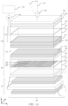
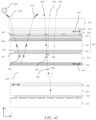
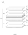
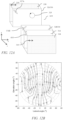
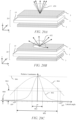
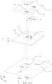
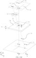
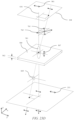
- FIGURE 1A is a schematic diagram illustrating in perspective side view a privacy display device 100 comprising a spatial light modulator 48 with an air gap input quarter waveplate 326; an air gap 619; an air gap output quarter waveplate 328, a switchable retarder stack 300 and an additional polariser 318; and
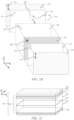
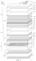
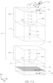
- FIGURE 1B is a schematic diagram illustrating in expanded view the arrangement of polarisers and retarders of FIGURE 1 .
- the display device 100 comprises a spatial light modulator 48; a display polariser 218 arranged on the output side of the spatial light modulator 48, the display polariser 218 being a linear polariser; an additional polariser 318 arranged on the output side of display polariser 218, the additional polariser 318 being a linear polariser; and plural polar direction control retarders 300 arranged between the additional polariser 318 and the display polariser 218, wherein an air gap 619 divides the plural polar direction control retarders 300 into at least one air gap input retarder 326 between the display polariser 218 and the air gap 619 and at least one air gap output retarder 328 between the air gap 619 and the additional polariser 318, the at least one air gap input retarder 326 being arranged to convert linearly polarised light passed by the display polariser 218 into circularly polarised light 325, and the plural polar direction control retarders 300 together being capable of simultaneously introducing no net, relative phase shift to orthogonal polarisation components of
- the plural control retarders 300 and additional polariser 318 do not affect the luminance of light from the display polariser 218 passing through the retarders 300 and the additional polariser 318 along an axis 199 along a normal to the plane of the retarders 300 and simultaneously the retarders 300 and additional polariser 318 do reduce the luminance of light from the display polariser 218 passing therethrough along an axis inclined to a normal to the plane of the retarders 300, at least in one of the switchable states of the switchable retarder 301.
- the plural polar direction control retarders 300 include at least one passive retarder.
- air gap input retarder 326, air gap output retarder 328, and passive polar direction control retarder 330 are passive retarders, while retarder 301 is a switchable liquid crystal retarder.
- the plural polar direction control retarders 300 include a switchable liquid crystal retarder 301 comprising a layer 314 of liquid crystal material.
- the at least one passive polar direction control retarder 330 comprises a passive retarder having an optical axis perpendicular to the plane of the retarder.
- the spatial light modulator 48 comprises a liquid crystal display comprising input polariser 210, output polariser 218 with substrates 212, 216, liquid crystal pixel layer 214 and red, green and blue pixels 220, 222, 224.
- the input electric vector transmission direction 211 at the input polariser 210 provides an input polarisation component that may be transformed by the liquid crystal pixel layer 214 to provide output polarisation component determined by the electric vector transmission direction 219 of the output polariser 218.
- Typical polarisers 210, 218, 318 may be linear polarisers such as dichroic polarisers.
- FIGURE 1B further illustrates that the retarders 326, 328, 330 have optical axis directions 327, 329, 408 respectively.
- the optical axis direction of the material in the layer 314 of liquid crystal material is determined by the voltage applied to the layer 314, as will be described further below.
- the display device 100 further comprises a backlight 20 arranged to output light, wherein the spatial light modulator 48 is a transmissive spatial light modulator arranged to receive output light from the backlight 20.
- Backlight 20 may be arranged to illuminate the spatial light modulator 48 and may comprise input light sources 15, waveguide 1, rear reflector 3 and optical stack 5 comprising diffusers, light turning films and other known optical backlight structures.
- Asymmetric diffusers that may comprise asymmetric surface relief features for example, may be provided in the optical stack 5 with increased diffusion in the elevation direction in comparison to the lateral direction may be provided.
- Advantageously image uniformity may be increased.
- the backlight 20 may be arranged to provide an angular light distribution that has reduced luminance for off-axis viewing positions in comparison to head-on luminance.
- a typical wide angle backlight has a roll-off at higher angles such that the full width half maximum of relative luminance may be preferably greater than 40°, more preferably greater than 60° and most preferably greater than 80°.
- the backlight 20 may provide a luminance at polar angles to the normal to the spatial light modulator greater than 45 degrees that is at most 33% of the luminance along the normal to the spatial light modulator, preferably at most 20% of the luminance along the normal to the spatial light modulator, and most preferably at most 10% of the luminance along the normal to the spatial light modulator.
- the luminance at polar angles to the normal to the spatial light modulator greater than 45 degrees may be at most 18%.
- the luminance for off-axis snoopers in a privacy display may be provided at sufficiently low levels, for example less than 1% and preferably less than 0.5%.
- a desirable visual security level can be achieved for high contrast images provided by the spatial light modulator 48.
- Backlight 20 may further comprise a switchable backlight arranged to switch the output angular luminance profile in order to provide reduced off-axis luminance in a privacy mode of operation and higher off-axis luminance in a public mode of operation.
- a switchable backlight arranged to switch the output angular luminance profile in order to provide reduced off-axis luminance in a privacy mode of operation and higher off-axis luminance in a public mode of operation.
- Such a directional backlight provides some off-axis luminance reduction, advantageously increasing head-on efficiency and reducing display visibility and stray light for off-axis locations.
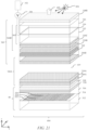
- the spatial light modulator 48 may alternatively be provided by other display types that provide output light 400 by emission, such as organic LED displays (OLED), with output polariser 218 in which case backlight 20 is omitted as will be illustrated in FIGURE 21 below.
- OLED organic LED displays
- the substrates 312, 316 of the switchable liquid crystal retarder 301 comprise electrodes arranged to provide a voltage across the layer 314 of liquid crystal material.
- Control system 352 is arranged to control the voltage applied by voltage driver 350 across the electrodes of the switchable liquid crystal retarder 301.
- Retarder 300 comprises a switchable liquid crystal retarder 301 comprising a layer 314 of liquid crystal material, and substrates 312, 316 arranged between the reflective polariser 302 and the additional polariser 318.
- a switchable liquid crystal retarder 301 comprising a layer 314 of liquid crystal material, and substrates 312, 316 arranged between the reflective polariser 302 and the additional polariser 318.
- An illustrative example for the arrangement of FIGURE 1A is given in TABLE 1.
- Retarder 300 further comprises a passive polar direction control retarder 330 as will be described further below.
- the switchable liquid crystal retarder 301 may comprise two surface alignment layers disposed adjacent to the layer 314 of liquid crystal material and on opposite sides thereof and each arranged to provide homeotropic alignment in the adjacent liquid crystal material.
- the layer 314 of liquid crystal material of the switchable liquid crystal retarder 301 may comprise a liquid crystal material with a negative dielectric anisotropy.
- the layer 314 of liquid crystal material may have a retardance for light of a wavelength of 550nm in a range from 500nm to 1000nm, preferably in a range from 600nm to 900nm and most preferably in a range from 700nm to 850nm.
- the at least one passive polar direction control retarder 330 may comprise a pair of retarders which have optical axes in the plane of the retarders that are crossed, each retarder of the pair of retarders having a retardance for light of a wavelength of 550nm in a range from 300nm to 800nm, preferably in a range from 500nm to 700nm and most preferably in a range from 550nm to 675nm.
- increased field of view in public mode of operation may be provided.
- zero voltage operation in public mode of operation may be provided, reducing power consumption.
- the switchable liquid crystal retarder 301 may comprise two surface alignment layers disposed adjacent to the layer 314 of liquid crystal material and on opposite sides thereof and each arranged to provide homogeneous alignment in the adjacent liquid crystal material.
- the switchable liquid crystal retarder 301 may comprise two surface alignment layers disposed adjacent to the layer 314 of liquid crystal material and on opposite sides thereof and each arranged to provide homogeneous alignment in the adjacent liquid crystal material.
- increased resilience to the visibility of flow of liquid crystal material during applied pressure may be achieved.
- the layer 314 of liquid crystal material of the switchable liquid crystal retarder 301 may comprise a liquid crystal material with a positive dielectric anisotropy.
- the layer 314 of liquid crystal material may have a retardance for light of a wavelength of 550nm in a range from 500nm to 900nm, preferably in a range from 600nm to 850nm and most preferably in a range from 700nm to 800nm.
- the at least one passive polar direction control retarder 330 may comprise a retarder having its optical axis perpendicular to the plane of the retarder, the at least one passive retarder having a retardance for light of a wavelength of 550nm in a range from -300nm to -700nm, preferably in a range from -350nm to - 600nm and most preferably in a range from -400nm to -500nm.
- the at least one passive polar direction control retarder 330 may comprise a pair of retarders which have optical axes in the plane of the retarders that are crossed, each retarder of the pair of retarders having a retardance for light of a wavelength of 550nm in a range from 300nm to 800nm, preferably in a range from 350nm to 650nm and most preferably in a range from 450nm to 550nm.
- a wavelength of 550nm in a range from 300nm to 800nm, preferably in a range from 350nm to 650nm and most preferably in a range from 450nm to 550nm.
- increased resilience to the visibility of flow of liquid crystal material during applied pressure may be achieved.
- the switchable liquid crystal retarder 301 may comprise two surface alignment layers disposed adjacent to the layer 314 of liquid crystal material and on opposite sides thereof, one of the surface alignment layers being arranged to provide homeotropic alignment in the adjacent liquid crystal material and the other of the surface alignment layers being arranged to provide homogeneous alignment in the adjacent liquid crystal material.
- the layer 314 of liquid crystal material may have a retardance for light of a wavelength of 550nm in a range from 700nm to 2000nm, preferably in a range from 1000nm to 1500nm and most preferably in a range from 1200nm to 1500nm.
- the at least one passive polar direction control retarder 330 may comprise a retarder having its optical axis perpendicular to the plane of the retarder, the at least one passive retarder having a retardance for light of a wavelength of 550nm in a range from -400nm to -1800nm, preferably in a range from -700nm to -1500nm and most preferably in a range from -900nm to -1300nm.
- the at least one passive polar direction control retarder 330 may comprise a pair of retarders which have optical axes in the plane of the retarders that are crossed, each retarder of the pair of retarders having a retardance for light of a wavelength of 550nm in a range from 400nm to 1800nm, preferably in a range from 700nm to 1500nm and most preferably in a range from 900nm to 1300nm.
- the layer 314 of liquid crystal material may have a retardance for light of a wavelength of 550nm in a range from 500nm to 1800nm, preferably in a range from 700nm to 1500nm and most preferably in a range from 900nm to 1350nm.
- the at least one passive polar direction control retarder 330 may comprise a retarder having its optical axis perpendicular to the plane of the retarder, the at least one passive retarder having a retardance for light of a wavelength of 550nm in a range from -300nm to -1600nm, preferably in a range from -500nm to -1300nm and most preferably in a range from -700nm to -1150nm.
- the at least one passive polar direction control retarder 330 may comprise a pair of retarders which have optical axes in the plane of the retarders that are crossed, each retarder of the pair of retarders having a retardance for light of a wavelength of 550nm in a range from 400nm to 1600nm, preferably in a range from 600nm to 1400nm and most preferably in a range from 800nm to 1300nm.
- a wavelength of 550nm in a range from 400nm to 1600nm, preferably in a range from 600nm to 1400nm and most preferably in a range from 800nm to 1300nm.
- increased resilience to the visibility of flow of liquid crystal material during applied pressure may be achieved.
- Each alignment layer may have a pretilt having a pretilt direction with a component in the plane of the liquid crystal layer that is parallel or anti-parallel or orthogonal to the electric vector transmission direction of the display polariser.
- a display may be provided with narrow viewing angle in a lateral direction and a wide viewing freedom for display rotation about a horizontal axis. Such a display may be comfortable to view for a head-on display user and difficult to view for an off-axis display user.
- the at least one passive retarder may comprise at least two passive retarders with at least two different orientations of optical axes which may have optical axes in the plane of the retarders that are crossed. Field of view for liquid crystal retarders with homogeneous alignment is increased while providing resilience to the visibility of flow of liquid crystal material during applied pressure.
- the pair of passive retarders may have optical axes that extend at 45° and at 135°, respectively, with respect to an electric vector transmission direction that is parallel to the electric vector transmission of the display polariser.
- the passive retarders may be provided using stretched films to advantageously achieve low cost and high uniformity.
- the switchable liquid crystal retarder 301 may be provided between the pair of passive retarders. Advantageously the thickness and complexity of the plural retarders may be reduced.
- a transparent electrode and a liquid crystal alignment layer may be formed on a side of each of the pair of passive retarders adjacent the switchable liquid crystal retarder 301; and may further comprise first and second substrates between which the switchable liquid crystal retarder 301 is provided, the first and second substrates each comprising one of the pair of passive retarders, wherein each of the pair of passive retarders has a retardance for light of a wavelength of 550nm in a range from 150nm to 800nm, preferably in a range from 200nm to 700nm and most preferably in a range from 250nm to 600nm.
- the at least one passive polar direction control retarder 330 may comprise a retarder having an optical axis perpendicular to the plane of the retarder.
- the thickness and complexity of the passive retarder stack may be reduced.
- the at least one passive polar direction control retarder 330 may comprise two passive retarders having an optical axis perpendicular to the plane of the passive retarders, and the switchable liquid crystal retarder 301 is provided between the two passive retarders.
- the thickness and complexity of the plural retarders may be reduced. High head-on efficiency may be achieved in both wide and privacy modes, a wide field of view for public mode and snoopers may be unable to perceive image data from a wide range of off-axis viewing locations.
- a transparent electrode and a liquid crystal alignment layer may be formed on a side of each of the two passive retarders adjacent the switchable liquid crystal retarder 301.
- the two passive retarders may have a total retardance for light of a wavelength of 550nm in a range from -300nm to -700nm, preferably in a range from -350nm to -600nm and most preferably in a range from -400nm to -500nm.
- the at least one passive polar direction control retarder 330 may comprise a retarder having an optical axis with a component perpendicular to the plane of the retarder and with a component in the plane of the retarder.
- Advantageously fields of view in public mode may be increased and snoopers may be unable to perceive image data from a wide range of off-axis viewing locations.
- the component in the plane of the passive retarder may extend at 0°, with respect to an electric vector transmission direction that is parallel or perpendicular to the electric vector transmission of the display polariser.
- the at least one passive retarder may further comprise a passive retarder having an optical axis perpendicular to the plane of the passive retarder or a pair of passive retarders which have optical axes in the plane of the passive retarders that are crossed.
- the retardance of the at least one passive polar direction control retarder 330 may be equal and opposite to the retardance of the switchable liquid crystal retarder 301.
- the plural polar direction control retarders 300 further comprise: an air gap input retarder 326 comprising at least one retarder arranged between the display polariser 218 and the air gap 619; and an air gap output retarder 328 comprising at least one retarder arranged between the air gap 619 and the additional polariser 318.
- the air gap input retarder 326 is arranged to provide a phase shift to provide a circularly polarised light component 325 in the air gap 619 of light passed by the display polariser 218 along an axis along a normal to the plane of the air gap input retarder 326.
- the retarders 300 do not affect the luminance of light passing through the reflective polariser 302, the retarders 300 and the additional polariser 318 along an axis along a normal to the plane of the retarders 300 but the retarders 300 do reduce the luminance of light passing therethrough along an axis inclined to a normal to the plane of the retarders 300, at least in one of the switchable states of the switchable retarder 301.
- the principles leading to this effect are described in greater detail below with reference to FIGURES 22A-26 and arises from the presence or absence of a phase shift introduced by the retarders 300 to light along axes that are angled differently with respect to the liquid crystal material of the retarders 300. A similar effect is achieved in all the devices described below.
- the display device 100 may further comprise a further additional polariser 318 and further polar direction control retarders (not shown) 300 arranged on the input side of the transmissive spatial light modulator 48 and between the backlight 20 and the spatial light modulator.
- the luminance may be further reduced for off-axis snoopers.
- wide angle backlights may be used so that viewing angle in public mode of operation may be increased, as described further below with respect to FIGURE 5 and FIGURE 8 .
- a view angle control optical element 360 for application to a display device comprising a spatial light modulator 48 and a display polariser 218 arranged on the output side of the spatial light modulator 48, the view angle control optical element 360 comprising a control polariser 318, being a linear polariser, and plural polar direction control retarders 300 for arrangement between the control polariser 318 and the display polariser 218 on application of the view angle control optical element 360 to the display device, wherein an air gap 619 divides the plural polar direction control retarders 300 into at least one air gap input retarder 326 and at least one air gap output retarder 328, the at least one air gap input retarder 326 being arranged to convert linearly polarised light passed by the display polariser 218 into circularly polarised light 325, and the plural polar direction control retarders 300 together being capable of simultaneously introducing no net, relative phase shift to orthogonal polarisation components of light passed by the display polariser 218 along an axis 199 along a normal to the plane of the
- a display apparatus may be fitted with a view angle control element 360 separately to the construction of the display.
- the fitting may be a retrofit.
- Image contrast due to frontal reflections for a head-on user may be optimised.
- Multiple spatial light modulators may be provided for a single view angle control element to increase display area. Thermal and mechanical variations between the spatial light modulator 48 and view angle control element 360 may be mitigated by using the air gap 619. Manufacturing yield may be increased in comparison to bonded optical components.
- FIGURE 2A is a schematic diagram illustrating in perspective side view a privacy display device comprising an emissive spatial light modulator with an output quarter waveplate; an air gap; an input quarter waveplate, a switchable retarder stack and an additional polariser, further comprising a reflective polariser; and
- FIGURE 2B is a schematic diagram illustrating in expanded view the arrangement of polarisers and retarders of FIGURE 2A .
- a reflective polariser 302 is arranged between the display polariser 218 and air gap input retarder 326, the reflective polariser 302 being a linear polariser.
- FIGURE 2A The structure of FIGURE 2A will now be described in more detail.
- the spatial light modulator 48 of FIGURE 2A comprises an emissive spatial light modulator in comparison to the transmissive spatial light modulator 48 and backlight 20 of FIGURE 1A .
- the emissive spatial light modulator 48 may comprise emissive pixels 220, 222, 224 that comprise organic LED (OLED) materials and/or inorganic LED (micro-LED) materials.
- the pixel layer 214 may further comprise a reflective surface. Undesirable reflections from the reflective surface may be reduced by means of quarter waveplate 221 arranged between the reflective pixel layer 214 and output polariser 218.
- Advantageously device thickness may be reduced in comparison to the arrangement of FIGURE 1A .
- output brightness may be increased.
- the display device 100 comprises: a spatial light modulator 48 arranged to output light 400; wherein the spatial light modulator 48 comprises an output polariser 218 arranged on the output side of the spatial light modulator 48; an additional polariser 318 arranged on the output side of the output polariser 218; a reflective polariser 302 arranged between the output polariser 218 and the additional polariser 318; and plural polar direction control retarders 300 arranged between the reflective polariser 302 and the additional polariser 318.
- the electric vector transmission direction 303 of the reflective polariser 302 is parallel to the electric vector transmission direction 319 of the additional polariser 318.
- the electric vector transmission direction 303 of the reflective polariser 302 is parallel to the electric vector transmission direction 219 of the output polariser 218.
- the display device may be arranged for use in ambient illumination 604.
- FIGURE 2C is a schematic diagram illustrating in expanded view an alternative arrangement of display polarisers 218, plural polar direction control retarders 326, 328, reflective polariser, 302 plural polar direction control retarders 300 and additional polariser 318 for a switchable privacy display.
- the reflective polariser is arranged on the output side of the air gap 619.
- the reflectivity of the display to ambient illumination 604 may be increased as will now be described.
- FIGURE 3A is a schematic diagram illustrating in side view propagation of output light from a spatial light modulator 48 through the optical stack of FIGURE 1A in a public mode of operation.
- light rays 400, 402 emitted by the backlight 20 in an on-axis direction have a polarisation component 359 parallel to the electric vector transmission direction 219 of the output polariser 218 on exiting the spatial light modulator 48.
- the on-axis ray 400 then traverses the plural polar direction control retarders 300 to the linear polarisation 362 which is the same as component 359.
- the switchable liquid crystal retarder 301 is in the off state where typically (but not necessarily) a voltage is not applied. In the case where the switchable liquid crystal retarder 301 has a positive dielectric anisotropy, the switchable liquid crystal retarder 301 therefore acts in a similar manner to an A-plate retarder in the first state.
- the on-axis light ray 400 therefore experiences minimal retardation when passing through the plural polar direction control retarders 300.
- the combined effect off the plural polar direction control retarders 300 results in the on-axis light ray 400 exiting the plural polar direction control retarders 300 with the same or similar linear polarisation 362 to the linear polarisation 359 with which the on-axis light ray 400 entered the plural polar direction control retarders 300.
- This linear polarisation 362 is parallel to the electric vector transmission direction 319 of the additional polariser 318 and the on-axis ray 400 therefore exits the display device 100 with a relatively unchanged luminance.
- the off-axis ray 402 traverses the plural polar direction control retarders 300 in a similar fashion to the on-axis ray 400.
- Polarisation 362 is substantially the same as polarisation 359 and polarisation 364 is substantially the same as polarisation 361.
- the angular transmission profile is substantially uniformly transmitting across a wide polar region.
- the plural polar direction control retarders 300 provide no overall retardance to light passing therethrough perpendicular to the plane of the retarders or at an acute angle to the perpendicular to the plane of the plural polar direction control retarders 300.
- the variation of display luminance with viewing angle in the first state is substantially unmodified. Multiple users may conveniently view the display from a wide range of viewing angles.
- FIGURE 3B is a schematic diagram illustrating in side view propagation of light rays from an ambient light source 604 through the optical stack of FIGURE 1A in a public mode of operation.
- the on-axis ray 410 of ambient light 604 traverses the plural polar direction control retarders 300 in a similar fashion to the on-axis ray 400 emitted from the backlight 20 discussed above.
- the on-axis ray 410 traverses the plural polar direction control retarders 300 in the reverse direction to the on-axis ray 400 emitted from the backlight 20, the traversal of the plural polar direction control retarders 300 in a reverse direction may not change the effect of the plural polar direction control retarders 300 on the light ray as discussed above for light emitted from the backlight 20.
- the on-axis ray 410 therefore reaches the backlight 20 where it may be absorbed or recirculated as emitted light 400 from the display device 100.
- the off-axis ray 402 experiences no overall transformation of polarisation when passing through the plural polar direction control retarders 300.
- Ambient light 604 is unpolarised and the off-axis light ray initially has no polarisation 370.
- the additional polariser 318 passes the polarisation 372 that is parallel to the electric vector transmission direction 319 of the additional polariser.
- the additional polariser 318 absorbs the majority of the polarisation 372 that is perpendicular to the electric vector transmission direction 319 of the additional polariser. Some light is reflected from the front surface of the polariser 318 by Fresnel reflections at the outer air interface.
- the linear polarisation 374 of the off-axis ray 402 is therefore parallel to the electric vector transmission direction 303 of the reflective polariser 302 and the off-axis ray is not reflected but instead passes the reflective polariser 302 to reach the spatial light modulator 448 where it may be absorbed by the input polariser 210 or transmitted into the backlight 20.
- the display reflectance in the public mode is reduced across a wide range of viewing angles. Multiple users may conveniently view the display from a wide range of viewing angles with high image contrast.
- FIGURE 3C is a schematic diagram illustrating in side view propagation of output light from a spatial light modulator 48 through the optical stack of FIGURE 1A in a privacy mode of operation.
- the switchable liquid crystal retarder 301 In the privacy mode, the switchable liquid crystal retarder 301 is in the on state where a voltage is applied to the liquid crystal layer 314. The switchable liquid crystal retarder 301 may therefore be in the second state of the said two states.
- the on-axis light ray 400 experiences no retardation when passing and has the same polarisation as the linear polarisation 362 after traversing the plural polar direction control retarders 300. The on-axis ray 400 therefore exits the display via the additional polariser 318 with a largely unchanged luminance in the privacy mode of operation.
- Off-axis light rays 402 emitted from the backlight 20 experience a transformation of polarisation when passing through plural polar direction control retarders 300. This is because of the acute angle of entry of the off-axis light ray 402, as discussed in further detail herein.
- the off-axis light ray 402 therefore arrives at the additional polariser 318 with a linear polarisation 364 that has polarisation components that have a relative phase shift.
- the linear polarisation 364 has at least some perpendicular component to the electric vector transmission direction 319 of the additional polariser 318 and the luminance of the off-axis light ray 402 is therefore reduced compared to the on-axis ray 400.
- the display luminance at wide viewing angles may be reduced in the second state. Snoopers may therefore be prevented from viewing the image emitted by the display device 100 at wide viewing angles. Stray light may be reduced in night-time operation while the head-on user may see an image.
- FIGURE 3D is a schematic diagram illustrating in side view propagation of light rays from an ambient light source 604 through the optical stack of FIGURE 1A in a privacy mode of operation.
- incident on-axis light rays 410 from the ambient light source 604 traverse the plural polar direction control retarders 300 in a similar fashion to the on-axis ray 400 emitted from the backlight 20 as described in relation to FIGURE 3C .
- the on-axis ray 410 traverses the plural polar direction control retarders 300 in the reverse direction to the on-axis ray 400 emitted from the backlight 20
- the direction of traversal of the plural polar direction control retarders 300 into or out of the display does not change the effect of the plural polar direction control retarders 300 on the light ray as discussed for light emitted from the backlight 20.
- the on-axis ray 410 therefore reaches the backlight 20 where it may be absorbed or recirculated as emitted light 400 from the display device 100.
- off-axis light rays 412 emitted from the backlight 20 experience a transformation of polarisation when passing through the plural polar direction control retarders 300. This is because of the acute angle of entry of the off-axis light ray 412, as discussed in further detail below.
- the off-axis light ray 412 therefore arrives at the reflective polariser 302 with a linear polarisation 374 that is at least partially rotated when compared to the linear polarisation 372.
- the linear polarisation 374 has at least some perpendicular component to the electric vector transmission direction 303 of the reflective polariser 302 and is therefore at least partially reflected by the reflective polariser 302.
- the ray 412 then traverses the plural polar direction control retarders 300 in the reverse direction, reversing the polarisation conversion from the first pass of the plural polar direction control retarders 300 and resulting in a polarisation 376 that is parallel to the electric vector transmission direction of the additional polariser 318.
- the off-axis ray 412 therefore leaves the display device 100 with polarisation 378, resulting in the stack appearing as a mirror when viewed from a wide angle.
- the additional polariser 318 absorbs the majority of the polarisation 372 that is perpendicular to the electric vector transmission direction 319 of the additional polariser, but may reflect a small proportion of the perpendicular component 404.
- the reflectance at wide viewing angles may be increased in the second state. Snoopers may therefore be prevented from viewing the image emitted by the display device 100 at wide viewing angles due to the reflected light reducing the contrast of the image being emitted by the display device, and so increasing visual security level, VSL as described in equation 4, above due to increased reflectivity, R.
- FIGURES 4A-B are schematic diagrams illustrating in side views surface reflections in a privacy display device 100 comprising a pair of quarter waveplates 326, 328 arranged on opposite sides of an air gap.
- FIGURE 4A illustrates the propagation of circularly polarised light for the arrangement of FIGURE 2C .
- the principles of operation of reflection reduction at the air gap 619 interfaces are common in the present embodiments.
- the air gap input retarder 326 is arranged on one side of the air gap 619 and air gap output retarder 328 is arranged on the opposite side of the air gap 619 and comprise respectively quarter waveplates.
- the first and second quarter waveplates of the air gap input and output retarders 326, 328 have optical axes that are crossed; and light 400 from the spatial light modulator 48 has a polarisation that undergoes equal and opposite phase shifts in the first and second crossed retarders 326 328.
- ambient light rays 623 are incident onto the reflective polariser 302 with a polarisation 630 that is substantially linear after transmission through the passive polar direction control retarder 330 and switchable liquid crystal layer 314.
- the polarisation 630 is parallel to the transmission electric vector direction of the reflective polariser 302 and is transmitted into the quarter waveplate of retarder 328 and undergoes a quarter wave phase shift to provide left circular polarisation 632.
- Quarter waveplate of retarder 328 provides an opposite phase shift for transmitted light ray 623 such that light is transmitted by polariser 218 and absorbed in the input polariser 210 or backlight 20 in the example of an LCD, or is extinguished by an optical isolator in the example of an OLED display.
- the opposite retarders 326, 328 also cancel each other, advantageously achieving high output efficiency.
- a display with high on-axis contrast and low off-axis contrast may be provided while providing an air gap to increase yield and reduce cost and complexity of assembly.
- FIGURE 4B differs from FIGURE 4A in that reflective polariser 302 is omitted, as illustrated in FIGURE 1A .
- a display with high on-axis contrast and low off-axis luminance may be provided while providing an air gap to increase yield and reduce cost and complexity of assembly.
- FIGURES 4A-B further illustrate that electrodes 500, 502 of a touch screen apparatus may be provided on the passive polar direction control retarder 330.
- electrodes 500, 502 of a touch screen apparatus may be provided on the passive polar direction control retarder 330.
- a compact touch screen apparatus with low reflectivity may be provided.
- FIGURE 4C is a schematic diagram illustrating in a side view surface reflections in a privacy display device with no pair of quarter waveplates.
- off-axis light rays 620 from external light source 604 are directed through the substrate 320 and directed through the retarders 300 towards the reflective polariser 302, at which the polarisation state 621 has polarisations that are orthogonal to the transmission direction of the reflective polariser 302.
- Air gap 619 provides Fresnel reflections at the air interfaces of the reflective polariser 302 and display polariser 218, as illustrated by rays 626, 628 that degrade contrast for the on-axis user.
- An index matched interface may be provided but reduces yield during manufacture.
- the backlight of FIGURE 1A may have a FWHM of less than 30 degrees, however desirably such displays have a FWHM of greater than 50 degrees.
- Switchable privacy displays may be provided with high visual security level in privacy mode and wide viewing freedom in privacy mode by stacking more than one plural retarder 300 and additional polariser 318 as will be described below.
- Such wide viewing freedom can be achieved from an emissive spatial light modulator 48 or a wide angle backlight 20 and transmissive spatial light modulator 48 as illustrated in FIGURE 1A .
- emissive spatial light modulator 48 or a wide angle backlight 20 and transmissive spatial light modulator 48 as illustrated in FIGURE 1A .
- more than one view angle control element 360 may be arranged with the display.
- Such a display can be expensive to assemble as a single bonded stack and so additional air gaps between component parts of the stack are desirable. It would be desirable to achieve high image contrast for such stacks of components for a head-on user in both privacy and public modes of operation.
- FIGURE 5 is a schematic diagram illustrating in perspective side view a privacy display device 100 comprising a spatial light modulator 48, first and second plural polar direction control retarders 300A, 300B, an additional polariser 318A and further additional polariser 318B; and
- FIGURE 6 is a schematic diagram illustrating in expanded view the arrangement of polarisers and retarders of FIGURE 5 .
- Air gap 619A is arranged between the spatial light modulator 48 and additional polariser 318A
- a second air gap 619B is arranged between the additional polariser 318A and further additional polariser 318B.
- the display device 100 thus further comprises a first-mentioned retarder 300A, a first-mentioned polariser 318A, at least one further retarder 300B and a further additional polariser 318B, wherein the at least one further retarder 300B is arranged between the first-mentioned additional polariser 318A and the further additional polariser 318B.
- the structure of the retarders 300A, 300B are each the same as the structure of the retarders 300 in FIGURE 1A and illustrated in TABLES 1-2.
- a backlight 20 with wide field of view may be provided for a transmissive spatial light modulator 48, or a wide field of view emissive spatial light modulator 48 may be provided.
- the display 100 may comprise a non-collimated (wide angle) backlight 20.
- Non-collimated backlights 20 may have reduced sensitivity to tooling and replication errors and may advantageously have reduced cost.
- the present embodiment may achieve very wide viewing angle and image uniformity in a public mode of operation, while having reduced assembly cost and complexity.
- the off-axis luminance may be increased, advantageously improving the image visibility to off-axis viewers in public mode. Further, the contrast for the head-on and off-axis users may be improved in public mode of operation. In privacy mode of operation, the contrast for the head-on user may be increased because reflections at air gaps are reduced. Further, the number of bonding steps during manufacture may be reduced and the yield increased.
- FIGURES 5-6 further illustrate that a diffuser structure may be used.
- a diffusing surface 346, 348 structure is provided on the air gap input retarder 326 and the air gap output retarder 328.
- Diffuser surfaces 346, 348 may be applied to at least some of the air gap input and output retarders 326A, 326B.
- the diffuser surfaces 346, 348 may be embossed structures formed on the retarders.
- Diffusers (not shown) may also be formed on the further additional polariser 318B and other layers within the structure such as retarders 326B, 328B.
- Advantageously the visibility of residual specular frontal reflections may be improved.
- air gap input retarders 326A, 326B and air gap output retarders 328A, 328B are arranged on opposite sides of the respective gap.
- the operation of the retarders for each gap is as illustrated above.
- Features of the embodiment of FIGURES 5-6 not discussed in further detail may be assumed to correspond to the features with equivalent reference numerals as discussed above, including any potential variations in the features.
- FIGURE 7 is a schematic diagram illustrating in perspective side views a view angle control element 360 for use in the privacy display device similar to FIGURES 5-6 .
- Features of the embodiment of FIGURE 7 not discussed in further detail may be assumed to correspond to the features with equivalent reference numerals as discussed above, including any potential variations in the features.
- Input retarder 328 is provided to the component 360 as an air gap output retarder for an air gap between the component and an air gap input retarder 326 arranged on the output polariser 218 of a spatial light modulator 48 (not shown).
- a high contrast switchable privacy display can be provided at low cost with a wide angle public mode and high visual security level for off-axis snoopers in privacy mode.
- FIGURE 5 A similar arrangement of FIGURE 5 wherein the plural polar direction control retarders 300 comprise crossed A-plates instead of a negative C-plate will now be described.
- FIGURE 8 is a schematic diagram illustrating in perspective side view a privacy display device comprising a spatial light modulator, first and second pairs of quarter waveplates, first and second switchable retarder stacks and an additional polariser and further additional polariser wherein the switchable retarder stacks comprise compensation retarders that are crossed A-plates; and
- FIGURE 9 is a schematic diagram illustrating in expanded view the arrangement of polarisers and retarders of FIGURE 1 .
- the pair of passive retarders 330A, 330B have optical axes that extend at 45° and at 135°, respectively, with respect to an electric vector transmission direction 219 that is parallel to the electric vector transmission of the display polariser 218.
- A-plates are simpler to manufacture and lower cost than C-plates.
- the switchable liquid crystal retarder 301 comprises two surface alignment layers disposed adjacent to the layer of liquid crystal material 314 and on opposite sides thereof and each arranged to provide homogeneous alignment in the adjacent liquid crystal material 314.
- the layer of liquid crystal material 314 of the switchable liquid crystal retarder 301 comprises a liquid crystal material 314 with a positive dielectric anisotropy.
- the layer of liquid crystal material 314 has a retardance for light of a wavelength of 550nm in a range from 500nm to 1000nm, preferably in a range from 600nm to 850nm and most preferably in a range from 700nm to 800nm.
- the homogeneous alignment of TABLE 3 may provide a display with improved resilience to applied stress. In particular relaxation times for homeotropic alignment are relatively long and may leave noticeable visual defects. While the illustrative embodiments below are provided by liquid crystal retarders 314 that use homogeneous alignment, homeotropic liquid crystal alignment similar to that illustrated in TABLE 1 may also be used. A lower drive voltage in public mode may be provided by homeotropic alignment, advantageously reducing power consumption.
- FIGURE 10A is a schematic diagram illustrating in expanded view an arrangement of polarisers and retarders comprising a pair of quarter waveplates either side of an air gap, crossed A-plates and a switchable liquid crystal retarder arranged between an output polariser and an additional polariser; and
- FIGURE 10B is a schematic graph illustrating the variation in transmission with polar direction for transmitted light rays in FIGURE 10A in a privacy mode of operation, with the illustrative embodiment of TABLE 4, where ⁇ o is the design wavelength of 540nm in this illustrative example.
- FIGURES 10A-B not discussed in further detail may be assumed to correspond to the features with equivalent reference numerals as discussed above, including any potential variations in the features.
- the two passive retarders 330A, 330B introduce no net, relative phase shift to orthogonal polarisation components of light passed by the display polariser 218 along an axis along a normal to the plane of the plural polar direction control retarders 300
- at least one compensation retarder comprises a further two passive retarders 330A, 330B which have optical axes 331A, 331B in the plane of the retarders that are crossed, the further two passive retarders 330A, 330B being respectively included in the at least one air gap output retarder 328 and the at least one air gap input retarder 326, the further two passive retarders 330A, 330B introducing no net, relative phase shift to orthogonal polarisation components of light passed by the display polariser 218 along an axis along a normal to the plane of the plural polar direction control retarders 300, and the one of the further two passive retarders 326 which is arranged in the at least one air gap retarder being arranged to convert linearly polarised light passed by the display polariser
- a display may be arranged to switch between a public and private mode of operation.
- Air gaps 619 may be provided while maintaining high contrast for on-axis images and increased manufacturing yield in comparison to arrangements wherein the plural polar direction control retarders 300 are bonded to the spatial light modulator 48.
- the retarders 326, 328 may be provided at low cost and complexity. In embodiments with crossed quarter wave retarders 326, 328 no net effect on retardance for on-axis and off-axis light rays is achieved.
- the reflection reduction at the air gap 619 is provided for off-axis viewing positions in public mode, achieving increased contrast.
- the A-plates of passive compensation retarder can further comprise at least one of the air gap input retarder 326 and air gap output retarder 328, as will now be described.
- FIGURE 10C is a schematic diagram illustrating in expanded view an arrangement of polarisers and retarders comprising a pair of quarter waveplates 326, 328 either side of an air gap 619, crossed A-plates 330A, 330B and a switchable liquid crystal retarder 314 arranged between an output polariser 218 and an additional polariser 318, wherein one of the A-plates 330A of the crossed A-plates comprises one of the pair of quarter waveplates 328; and
- FIGURE 10D is a schematic graph illustrating the variation in transmission with polar direction for transmitted light rays in FIGURE 10C in a privacy mode of operation, with the illustrative embodiment of TABLE 5.
- retarder 328330 has a retardance of the passive polar direction control retarder 330A minus the retardance of air gap output retarder 328, as illustrated in TABLE 5 for the illustrative nominal wavelength of 540nm.
- the two passive retarders 330A, 330B introduce no net, relative phase shift to orthogonal polarisation components of light passed by the display polariser 218 along an axis 199 along a normal to the plane of the plural polar direction control retarders 300
- the at least one passive compensation retarder comprises a further two passive retarders 326, 328 which have optical axes in the plane of the retarders that are crossed, the further two passive retarders being respectively included in the at least one air gap output retarder and the at least one air gap input retarder, the further two passive retarders introducing no net, relative phase shift to orthogonal polarisation components of light passed by the display polariser along an axis along a normal to the plane of the plural polar direction control retarders, and the one of the further two passive retarders which is arranged in the at least one air gap retarder being arranged to convert linearly polarised light passed by the display polariser into circularly polarised light.
- One of the two passive retarders has a retardance for light of a wavelength of 550nm in a range from 150nm to 800nm, preferably in a range from 200nm to 700nm and most preferably in a range from 250nm to 600nm.
- Said one of the two passive retarders and the further passive retarder have optical axes in the plane of the retarders that are crossed, and the other of the two passive retarders has a retardance for light of a wavelength of 550nm that is equal to the retardance of said one of the two passive retarders minus the retardance of the further passive retarder.
- Retarder 328330 comprises the retardance of the passive polar direction control retarder 330A of FIGURE 10A minus the retardance of the retarder 328 in FIGURE 10A .
- the circular polarisation 325 in the air gap 619 as illustrated in FIGURES 4A-B are converted to the appropriate linear polarisation state at the additional polariser 318.
- FIGURE 11A is a schematic diagram illustrating in expanded view an arrangement of polarisers and retarders comprising a pair of quarter waveplates either side of an air gap, crossed A-plates and a switchable liquid crystal retarder arranged between an output polariser and an additional polariser; and
- FIGURE 11B is a schematic graph illustrating the variation in transmission with polar direction for transmitted light rays in FIGURE 11A in a privacy mode of operation, with the illustrative embodiment of TABLE 6.
- the two passive retarders 326, 328 introduce no net, relative phase shift to orthogonal polarisation components of light passed by the display polariser 218 along an axis along a normal to the plane of the plural polar direction control retarders 300
- at least one compensation retarder comprises a further two passive retarders 330A, 330B which have optical axes 331A, 331B in the plane of the retarders that are crossed, the further two passive retarders 330A, 330B being respectively included in the at least one air gap output retarder 328 and the at least one air gap input retarder 326, the further two passive retarders 330A, 330B introducing no net, relative phase shift to orthogonal polarisation components of light passed by the display polariser 218 along an axis along a normal to the plane of the plural polar direction control retarders 300, and the one of the further two passive retarders 326 which is arranged in the at least one air gap retarder being arranged to convert linearly polarised light passed by the display polariser 218
- FIGURE 11C is a schematic diagram illustrating in expanded view an arrangement of polarisers and retarders comprising a pair of quarter waveplates either side of an air gap, crossed A-plates and a switchable liquid crystal retarder arranged between an output polariser and an additional polariser, wherein one of the A-plates of the crossed A-plates comprises one of the pair of quarter waveplates; and
- FIGURE 11D is a schematic graph illustrating the variation in transmission with polar direction for transmitted light rays in FIGURE 11C in a privacy mode of operation, with the illustrative embodiment of TABLE 7.
- FIGURES 11C-D not discussed in further detail may be assumed to correspond to the features with equivalent reference numerals as discussed above, including any potential variations in the features.
- the plural polar direction control retarders 300 introduce no net, relative phase shift to orthogonal polarisation components of light passed by the display polariser 218 along an axis along a normal to the plane of the plural polar direction control retarders 300, and at least one passive polar direction control retarder 330 comprises a further two passive retarders 328330, 330B which have optical axes in the plane of the retarders that are crossed.
- the further two passive retarders are respectively included in the at least one air gap output retarder 328 and the at least one air gap input retarder 326, the further two passive retarders introducing no net, relative phase shift to orthogonal polarisation components of light passed by the display polariser 218 along an axis along a normal to the plane of the plural polar direction control retarders 300, and the one of the further two passive retarders 326 which is arranged in the at least one air gap retarder 326 being arranged to convert linearly polarised light passed by the display polariser 218 into circularly polarised light 325.
- Said one of the two passive retarders and the further passive retarder have optical axes in the plane of the retarders that are aligned, and the other of the two passive retarders has a retardance for light of a wavelength of 550nm that is equal to the retardance of said one of the two passive retarders plus the retardance of the further passive retarder.
- the plural polar direction control retarders 300 include a switchable liquid crystal retarder comprising a layer of liquid crystal material, the switchable liquid crystal retarder being provided between the pair of passive retarders.
- the display device further comprises a transparent electrode and a liquid crystal alignment layer formed on a side of each of the pair of passive retarders adjacent the switchable liquid crystal retarder.
- the display device further comprises first and second substrates between which the switchable liquid crystal retarder is provided, the first and second substrates each comprising one of the pair of passive retarders.
- the two passive retarders are respectively included in the at least one air gap output retarder and the at least one air gap input retarder.
- FIGURE 12A is a schematic diagram illustrating in expanded view an arrangement of polarisers and retarders comprising crossed A-plates 326330, 328330 that operate as multiple order quarter waveplates either side of an air gap 619 and a switchable liquid crystal retarder 314 arranged between an output polariser and an additional polariser; and
- FIGURE 12B is a schematic graph illustrating the variation in transmission with polar direction for transmitted light rays in FIGURE 11A in a privacy mode of operation for the illustrative embodiment of TABLE 8.
- FIGURES 12A-B not discussed in further detail may be assumed to correspond to the features with equivalent reference numerals as discussed above, including any potential variations in the features.
- the circular polarisation 325 is provided by the first compensation retarder 326330.
- the second compensation retarder 328330 that is crossed with retarder 328330 provides the desirable viewing angle characteristics.
- the retardance of the retarders 326330 and 328330 is increased in comparison to zero order quarter waveplates 326, 328 of other illustrative embodiments herein.
- Advantageously cost and complexity is reduced while a switchable privacy display is achieved.
- FIGURE 13 is a schematic graph illustrating the variation in reflectivity with wavelength for reflected light rays at air interface 619, with the illustrative embodiments of TABLE 8 for profile 472 and TABLE 4 for profile 470. Additional colouration is provided for the circular polarisation 325 in FIGURE 12A in comparison to the colouration of polarisation 325 in FIGURE 10A .
- FIGURE 14 is a schematic diagram illustrating in expanded view an arrangement of polarisers and retarders comprising a pair of quarter waveplates either side of an air gap, crossed A-plates and a switchable liquid crystal retarder arranged between an output polariser and an additional polariser further comprising a half wave retarder arranged to rotate the polarisation component from the output polariser, with the illustrative embodiment of TABLE 9.
- polarisers and retarders comprising a pair of quarter waveplates either side of an air gap, crossed A-plates and a switchable liquid crystal retarder arranged between an output polariser and an additional polariser further comprising a half wave retarder arranged to rotate the polarisation component from the output polariser
- the display polariser 218 and the additional polariser 318 have electric vector transmission directions 219, 319 that are not parallel, and the display device 100 further comprises a rotator retarder 336 arranged between the additional polariser 318 and the display polariser 218, the rotator retarder 336 being arrange to rotate a polarisation direction of polarised light incident thereon between the electric vector transmission directions of the display polariser 218 and the additional polariser 318.
- the spatial light modulator 48 includes a layer 214 of twisted nematic liquid crystal material.
- a switchable privacy display may be provided for a twisted nematic LCD while maintaining a lateral roll-off in viewing angle in privacy mode and low reflection from air gaps 619.
- FIGURE 15 is a schematic diagram illustrating in expanded view an arrangement of polarisers and retarders comprising a pair of quarter waveplates either side of an air gap, crossed A-plates and a switchable liquid crystal retarder arranged between an output polariser and an additional polariser, wherein one of the A-plates of the crossed A-plates comprises one of the pair of quarter waveplates further comprising a half wave retarder arranged to rotate the polarisation component from the output polariser , with the illustrative embodiment of TABLE 10.
- FIG. 15 not discussed in further detail may be assumed to correspond to the features with equivalent reference numerals as discussed above, including any potential variations in the features.
- FIGURE 10C Such an arrangement provides the advantages of FIGURE 10C for example while providing a switchable privacy display for a twisted nematic LCD.
- the embodiments above have been described for switchable privacy displays. It may be desirable to provide non-switchable displays.
- the embodiments above have also described privacy displays with a luminance and reflectivity roll-off in a lateral direction. It may be desirable to provide luminance and reflectivity variations that are operable in both landscape and portrait display orientations for example, that is polar luminance and reflectivity profiles that have some degree of circular symmetry.
- FIGURE 16A is a schematic diagram illustrating in perspective side view an arrangement of a negative C-plate retarder arranged between quarter waveplates and a reflective polariser arranged between parallel polarisers wherein an air gap is arranged between the negative C-plate and one of the quarter waveplates;
- FIGURE 16B is a schematic graph illustrating the variation of transmission with polar direction for the transmitted light rays for the arrangement of FIGURE 16A ;
- FIGURE 16C is a schematic graph illustrating the variation of reflectivity with polar direction for the reflected light rays for the arrangement of FIGURE 16A , with the illustrative embodiment of TABLE 11.
- FIGURES 16A-C not discussed in further detail may be assumed to correspond to the features with equivalent reference numerals as discussed above, including any potential variations in the features.
- the plural polar direction control retarders 300 further comprise two passive retarders 296A, 296B which have optical axes in the plane of the retarders that are crossed, the two passive retarders being respectively included in the at least one air gap output retarder 330, 296B and the at least one air gap input retarder 296A, the two passive retarders 296A, 296B introducing no net, relative phase shift to orthogonal polarisation components of light passed by the display polariser along an axis 199 along a normal to the plane of the plural polar direction control retarders 300, and the one of the two passive retarders 296A which is arranged in the at least one air gap retarder being arranged to convert linearly polarised light passed by the display polariser 218 into circularly polarised light 325.
- the at least one passive polar direction control retarder 330 comprises a retarder having an optical axis with a component perpendicular to the plane of the retarder.
- the passive retarder 330 having an optical axis perpendicular to the plane of the retarder has a retardance for light of a wavelength of 550nm in a range from -400nm to -1000nm and preferably in a range from -750nm to - 850nm.
- the polar profile of FIGURE 16C illustrates the reflectivity of the display including the reflective polariser 302 and front surface Fresnel reflections from the additional polariser 318. Peak reflectivity of approximately 50% may be achieved, ignoring absorption of the transmitted polarisation at the polariser 318 for ambient light.
- FIGURE 16A can advantageously provide operation in landscape and portrait operations of a display, or privacy for a snooper looking down onto the display device 100. Further reduced cost and thickness can be achieved in comparison to the arrangements comprising a switchable liquid crystal retarder 301 described above.
- Such an element may be used to condition the angular output of a display with a wide angular range, such as an emissive display. Image contrast to the head-on user may be maintained when air gap 619 is used.
- FIGURE 17A is a schematic diagram illustrating in perspective side view an arrangement of a positive C-plate retarder arranged between quarter waveplates and a reflective polariser arranged between parallel polarisers;
- FIGURE 17B is a schematic graph illustrating the variation of transmission with polar direction for the transmitted light rays for the arrangement of FIGURE 17A ;
- FIGURE 17C is a schematic graph illustrating the variation of reflectivity with polar direction for the reflected light rays for the arrangement of FIGURE 17A , with the illustrative embodiment of TABLE 12.
- FIGURE 17A-C not discussed in further detail may be assumed to correspond to the features with equivalent reference numerals as discussed above, including any potential variations in the features.
- the at least one passive polar direction control retarder 330 comprises a retarder having an optical axis with a component perpendicular to the plane of the retarder.
- the passive retarder 330 having an optical axis perpendicular to the plane of the retarder has a retardance for light of a wavelength of 550nm in a range from +500nm to +1200nm and preferably in a range from +950nm to +1050nm.
- FIGURE 17A The operation of FIGURE 17A is similar to that of FIGURE 16A other than a positive C-plate is used in place of a negative C-plate. Improved polar profile may be achieved for luminance and reflectivity. Similar advantages to those of FIGURE 16A are obtained.
- A-plates are more conveniently manufactured than C-plates. It would be desirable to provide a passive structure with A-plates.
- FIGURE 18A is a schematic diagram illustrating in side perspective view an example of a passive retarder stack comprising a passive control retarder, comprising a series of four aligned A-plates; and FIGURE 18B is a schematic graph illustrating the variation of transmission with polar direction for the transmitted light rays for the arrangement of FIGURE 18A , with the illustrative embodiment of TABLE 13.
- FIGURES 18A-B may be assumed to correspond to the features with equivalent reference numerals as discussed above, including any potential variations in the features.
- the at least one passive retarder 330 may comprise a pair of passive retarders 330B, 330C which have optical axes in the plane of the passive retarders that are crossed.
- the two passive retarders 326, 328 introduce no net, relative phase shift to orthogonal polarisation components of light passed by the display polariser 218 along an axis along a normal to the plane of the plural polar direction control retarders 300
- at least one compensation retarder comprises a further two passive retarders 330A, 330B which have optical axes 331A, 331B in the plane of the retarders that are crossed, the further two passive retarders 330A, 330B being respectively included in the at least one air gap output retarder 328 and the at least one air gap input retarder 326, the further two passive retarders 330A, 330B introducing no net, relative phase shift to orthogonal polarisation components of light passed by the display polariser 218 along an axis along a normal to the plane of the plural polar direction control retarders 300, and the one of the further two passive retarders 326 which is arranged in the at least one air gap retarder being arranged to convert linearly polarised light passed by the display polariser 218
- FIGURE 18A The operation of FIGURE 18A is similar to that of FIGURE 16A and FIGURE 17A with similar application and advantages.
- A-plates are more convenient to manufacture than C-plates so that lower cost may be achieved.
- FIGURE 19A is a schematic diagram illustrating in a side view the structure of part of a switchable privacy display device 100 comprising touch electrode arrays 500, 502 arranged on facing surfaces of a pair of crossed passive polar direction control retarders 330A, 330B wherein the air gap 619 is between the display polariser 218 and the switchable liquid crystal retarder 301.
- FIGURE 19A is similar in structure to that of FIGURES 4A-B .
- the touch electrode arrays 500, 502 are arranged on the facing surfaces of the passive retarders 330A, 330B that may have the advantages described above.
- a dielectric layer 504 comprising dielectric material 507 is arranged between the electrode arrays 500, 502 and may for example be an adhesive.
- Touch electrode arrays 500, 502 may comprise transparent conductors for example ITO, silver nanowires or conductive polymers. They may be formed by know techniques including physical vapour deposition, sputtering, evaporation, ink-jet printing or contact printing. They may be patterned by the use of masks or photo resists and etching. When the electrodes are formed on the flexible retarder substrates, for example PC or COC/COP, then the type and temperature of the electrode deposition process may be controlled to avoid melting or the substrate. Inherently low temperature processes such as ink-jet and contact printing can produce electrode layers without exceeding the glass transition temperature of the substrates.
- the electrode arrays 500, 502 may be conveniently formed on the retarders 330A, 330B and low tolerance alignment may be provided between the two layers. Advantageously cost may be reduced while high contrast is maintained and touch screen operation enabled.
- FIGURE 19B is a schematic diagram illustrating in a side view the structure of part of a switchable privacy display device 100 comprising touch electrode arrays arranged on facing surfaces of a pair of crossed passive polar direction control retarders 330A, 330B wherein the air gap 619 is between the switchable liquid crystal retarder 301 and the additional polariser 318.
- FIGURE 19B is similar to FIGURE 19A , however the air gap 619 is located above the switchable liquid crystal retarder 301.
- the arrangement of polar direction control retarders 328330, 330B and air gap input quarter waveplate 326 as described previously may be provided.
- Advantageously the thickness and weight of the suspended touch screen element is reduced.
- FIGURE 19C is a schematic diagram illustrating in a side view the structure of part of a switchable privacy display device 100 comprising a touch electrode array 500 arranged on one surface of one of a pair of crossed passive polar direction control retarders wherein the air gap 619 is between the switchable liquid crystal retarder 301 and the additional polariser 318.
- FIGURE 19C is similar to the arrangement of FIGURE 19B , however a non-birefringent substrate 370 is provided for one of the touch screen electrode arrays.
- Substrate 370 may alternatively have an optical axis that is parallel or orthogonal to the electric vector transmission direction of the additional polariser 318.
- the polar direction control retarders may be provided on the substrate 316 of the switchable liquid crystal retarder 301.
- FIGURE 19D is a schematic diagram illustrating in a side view the structure of part of a switchable privacy display device 100 comprising touch electrode arrays 500, 502 that is not arranged on the passive polar direction control retarders 330A, 330B wherein the air gap 619 is between the switchable liquid crystal retarder 301 and the additional polariser 318.
- FIGURE 19D is similar to FIGURE 19C , but no touch screen electrodes are provided on retarders, and are provided on non-birefringent substrates 370, 372 (or substrates with optical axes aligned parallel or orthogonal to the electric vector transmission direction of the additional polariser 318).
- Electrode arrays 500, 502 may be arranged on substrates 370, 372 that are better suited to forming electrodes than the passive polar direction control retarders 330 or air gap quarter waveplates 326, 328, or polarisation rotation retarders 336.
- the formation of electrode arrays 500, 502 may be cheaper and have higher reliability and performance.
- FIGURE 20A is a schematic diagram illustrating in front perspective view a directional backlight
- FIGURE 20B is a schematic diagram illustrating in front perspective view a non-directional backlight 20, either of which may be applied in any of the devices described herein.
- a directional backlight 20 as shown in FIGURE 20A provides a narrow cone 450
- a non-directional backlight 20 as shown in FIGURE 20B provides a wide angular distribution cone 452 of light output rays.
- FIGURE 20C is a schematic graph illustrating variation with luminance with lateral viewing angle for various different backlight arrangements.
- the graph of FIGURE 20C may be a cross section through the polar field-of-view profiles described herein.
- a Lambertian backlight has a luminance profile 846 that is independent of viewing angle.
- a typical wide angle backlight has a roll-off 844 at higher angles such that the full width half maximum 866 of relative luminance may be greater than 40°, preferably greater than 60° and most preferably greater than 80°. Further the relative luminance 864 at +/-45°, is preferably greater than 7.5%, more preferably greater than 10% and most preferably greater than 20%.
- a directional backlight 20 has a roll-off at higher angles such that the full width half maximum 862 of relative luminance may be less than 60°, preferably less than 40° and most preferably less than 20°.
- the backlight 20 may provide a luminance at polar angles to the normal to the spatial light modulator 48 greater than 45 degrees that is at most 33% of the luminance along the normal to the spatial light modulator 48, preferably at most 20% of the luminance along the normal to the spatial light modulator 48, and most preferably at most 10% of the luminance along the normal to the spatial light modulator 48.
- Scatter and diffraction in the spatial light modulator 48 may degrade privacy mode operation when the switchable retarder 300 is arranged between the input display polariser 210 and additional polariser 318.
- the luminance at polar angles to the normal to the spatial light modulator greater than 45 degrees may be increased in arrangements wherein the switchable retarder 300 is arranged between the output display polariser 218 and additional polariser 318 in comparison to arrangements wherein the switchable retarder 300 is arranged between the input display polariser 210 and additional polariser 318.
- FIGURE 20D is a schematic diagram illustrating in side view a switchable directional display apparatus 100 comprising a switchable liquid crystal retarder 300 and backlight 20.
- the backlight 20 of FIGURE 20D may be applied in any of the devices described herein and which comprises an imaging waveguide 1 illuminated by a light source array 15 through an input end 2.
- FIGURE 20E which is a schematic diagram illustrating in rear perspective view operation of the imaging waveguide 1 of FIGURE 20D in a narrow angle mode of operation.
- the imaging waveguides 1 is of the type described in U.S. Patent No. 9,519,153 .
- the waveguide 1 has an input end 2 extending in a lateral direction along the waveguide 1.
- An array of light sources 15 are disposed along the input end 2 and input light into the waveguide 1.
- the waveguide 1 also has opposed first and second guide surfaces 6, 8 extending across the waveguide 1 from the input end 2 to a reflective end 4 for guiding light input at the input end 2 forwards and back along the waveguide 1.
- the second guide surface 8 has a plurality of light extraction features 12 facing the reflective end 4 and arranged to deflect at least some of the light guided back through the waveguide 1 from the reflective end 4 from different input positions across the input end 2 in different directions through the first guide surface 6 that are dependent on the input position.
- light rays are directed from light source array 15 through an input end and are guided between first and second guiding surfaces 6, 8 without loss to a reflective end 4. Reflected rays are incident onto facets 12 and output by reflection as light rays 230 or transmitted as light rays 232. Transmitted light rays 232 are directed back through the waveguide 1 by facets 803, 805 of rear reflector 800. Operation of rear reflectors are described further in U.S. Patent No. 10,054,732 .
- optical power of the curved reflective end 4 and facets 12 provide an optical window 26 that is transmitted through the spatial light modulator 48 and has an axis 197 that is typically aligned to the optical axis 199 of the waveguide 1. Similar optical window 26 is provided by transmitted light rays 232 that are reflected by the rear reflector 800.
- FIGURE 20F is a schematic graph illustrating field-of-view luminance plot of the output of FIGURE 20E when used in a display apparatus with no switchable liquid crystal retarder.
- off-axis viewing positions observed by snoopers 47 may have reduced luminance, for example between 1% and 3% of the central peak luminance at an elevation of 0 degrees and lateral angle of +/-45 degrees. Further reduction of off-axis luminance is achieved by the plural retarders 301, 330 of the present embodiments.
- FIGURE 20G is a schematic diagram illustrating in side view a switchable directional display apparatus comprising a backlight 20 including a switchable collimating waveguide 901 and a switchable liquid crystal retarder 300 and additional polariser 318.
- the backlight 20 of FIGURE 20G may be applied in any of the devices described herein and is arranged as follows.
- the waveguide 901 has an input end 902 extending in a lateral direction along the waveguide 901.
- An array of light sources 915 are disposed along the input end 902 and input light into the waveguide 1.
- the waveguide 901 also has opposed first and second guide surfaces 906, 908 extending across the waveguide 1 from the input end 2 to a reflective end 4 for guiding light input at the input end 2 forwards and back along the waveguide 1. In operation, light is guided between the first and second guiding surface 906, 908.
- the first guiding surface 906 may be provided with a lenticular structure 904 comprising a plurality of elongate lenticular elements 905 and the second guiding surface 908 may be provided with prismatic structures 912 which are inclined and act as light extraction features.
- the plurality of elongate lenticular elements 905 of the lenticular structure 904 and the plurality of inclined light extraction features deflect input light guided through the waveguide 901 to exit through the first guide surface 906.
- a rear reflector 903 that may be a planar reflector is provided to direct light that is transmitted through the surface 908 back through the waveguide 901.
- Output light rays that are incident on both the prismatic structures 912 and lenticular elements 905 of the lenticular structure 904 are output at angles close to grazing incidence to the surface 906.
- a prismatic turning film 926 comprising facets 927 is arranged to redirect output light rays 234 by total internal reflection through the spatial light modulator 48 and compensated switchable liquid crystal retarder 300.
- FIGURE 20H is a schematic diagram illustrating in top view output of the collimating waveguide 901.
- Prismatic structures 912 are arranged to provide light at angles of incidence onto the lenticular structure 904 that are below the critical angle and thus may escape. On incidence at the edges of a lenticular surface, the inclination of the surface provides a light deflection for escaping rays and provides a collimating effect.
- Light ray 234 may be provided by light rays 188a-c and light rays 189a-c, with incidence on locations 185 of the lenticular structure 904 of the collimated waveguide 901.
- FIGURE 20I is a schematic graph illustrating an iso-luminance field-of-view polar plot for the display apparatus of FIGURE 20G .
- a narrow output light cone may be provided, with size determined by the structures 904, 912 and the turning film 926.
- the luminance of output from the display is small, typically less than 2%. It would be desirable to achieve further reduction of output luminance. Such further reduction is provided by the compensated switchable liquid crystal retarder 300 and additional polariser 318 as illustrated in FIGURE 20G .
- a high performance privacy display with low off-axis luminance may be provided over a wide field of view.
- Directional backlights such as the types described in FIGURE 20D and FIGURE 20G together with the plural retarders 301, 330 of the present embodiments may achieve off-axis luminance of less than 1.5%, preferably less than 0.75% and most preferably less than 0.5% may be achieved for typical snooper 47 locations. Further, high on-axis luminance and uniformity may be provided for the primary user 45.
- a high performance privacy display with low off-axis luminance may be provided over a wide field of view, that may be switched to a wide angle mode by means of control of the switchable retarder 301 by means of control system 352.
- FIGURE 21 is a schematic diagram illustrating in side perspective view an example of an emissive switchable privacy display 604 comprising an emissive spatial light modulator 48, output polariser 218, crossed quarter waveplates 296A, 296B on opposites sides of an air gap 619, passive retarder 330A, additional polariser that is a reflective polariser 302, crossed A-plates 330B, 330C, switchable liquid crystal retarder 301 and further additional polariser 318, with the illustrative embodiment of TABLE 14.
- FIGURES 21 not discussed in further detail may be assumed to correspond to the features with equivalent reference numerals as discussed above, including any potential variations in the features.
- the spatial light modulator may comprise an emissive spatial light modulator 48 arranged to output light.
- the display polariser 218 may be an output display polariser arranged on the output side of the emissive spatial light modulator 48.
- Advantageously display thickness may be reduced in comparison to displays with backlights, and flexible and bendable displays may be conveniently provided.
- the spatial light modulator may have a pixel layer 514, support substrates 512, 516.
- the pixel layer 514 may be partially reflective to incident ambient light so that a quarter waveplate retarder 518 may be provided between the display polariser 218 and the pixel layer 514 to minimise reflection.
- the retarder 518 is different in operation to the retarders of the present retarders disclosed elsewhere herein and does not provide circular symmetry to polar output profiles or reduction of reflectivity at air gaps.
- Such an emissive display typically provides high angular range of optical output, that may be Lambertian or similar to Lambertian in profile.
- multiple view angle control retarders 300A, 300B, and additional polariser 318A, and further additional polariser 318B may be provided.
- the additional polariser 318A is provided by the reflective polariser 302, that is the dichroic polariser 318A illustrated elsewhere herein is omitted.
- Advantageously cost and thickness is reduced, and efficiency is increased.
- the first plural polar direction control retarders 300A are passive retarders 296A, 330A, 296B of the type illustrated in FIGURE 16A , FIGURE 17A or FIGURE 18A , and thus achieve a restricted angular luminance profile for light from the display in both public and privacy modes of operation.
- the plural polar direction control retarders 300B are arranged to provide switching between privacy and public modes of operation as described elsewhere herein.
- an emissive display may be provide with an air spaced view angle control element 360 that is spaced by air gap 619 from the emissive spatial light modulator 48 without reduction of head-on contrast to the primary user in both privacy and public modes of operation.
- At least one retarder is arranged between the reflective polariser 318 and the additional polariser 218 in various different configurations.
- the at least one retarder is configured so that it does not affect the luminance of light passing through the reflective polariser 318, the at least one retarder, and the additional polariser 218 along an axis along a normal to the plane of the retarder(s) but it does reduce the luminance of light passing through the reflective polariser 318, the at least one retarder, and the additional polariser 218 along an axis inclined to a normal to the plane of the retarder(s), at least in one of the switchable states of the compensated switchable retarder 300.
- FIGURE 22A is a schematic diagram illustrating in perspective view illumination of a retarder layer by off-axis light.
- Correction retarder 630 may comprise birefringent material, represented by refractive index ellipsoid 632 with optical axis direction 634 at 0 degrees to the x-axis, and have a thickness 631.
- Normal light rays 636 propagate so that the path length in the material is the same as the thickness 631.
- Light rays 637 are in the y-z plane have an increased path length; however the birefringence of the material is substantially the same as the rays 636.
- By way of comparison light rays 638 that are in the x-z plane have an increased path length in the birefringent material and further the birefringence is different to the normal ray 636.
- the retardance of the retarder 630 is thus dependent on the angle of incidence of the respective ray, and the plane of incidence, that is rays 638 in the x-z will have a retardance different from the normal rays 636 and the rays 637 in the y-z plane.
- FIGURE 22B is a schematic diagram illustrating in perspective view illumination of a retarder layer by off-axis light of a third linear polarization state at 90 degrees to the x-axis
- FIGURE 22C is a schematic diagram illustrating in perspective view illumination of a retarder layer by off-axis light of a fourth linear polarization state at 0 degrees to the x-axis.
- the incident linear polarization states are aligned to the optical axes of the birefringent material, represented by ellipse 632. Consequently, no phase difference between the third and fourth orthogonal polarization components is provided, and there is no resultant change of the polarization state of the linearly polarized input for each ray 636, 637, 638.
- the retarder 630 introduces no phase shift to polarisation components of light passed by the polariser on the input side of the retarder 630 along an axis along a normal to the plane of the retarder 630. Accordingly, the retarder 630 does not affect the luminance of light passing through the retarder 630 and polarisers (not shown) on each side of the retarder 630.
- FIGURES 29A-C relate specifically to the retarder 630 that is passive, a similar effect is achieved by the retarders in the devices described above.
- FIGURE 22D is a schematic diagram illustrating in perspective view illumination of a retarder 630 layer by off-axis light of a linear polarization state at 45 degrees.
- the linear polarization state may be resolved into third and fourth polarization components that are respectively orthogonal and parallel to optical axis 634 direction.
- the retarder thickness 631 and material retardance represented by refractive index ellipsoid 632 may provide a net effect of relatively shifting the phase of the third and fourth polarization components incident thereon in a normal direction represented by ray 636 by half a wavelength, for a design wavelength.
- the design wavelength may for example be in the range of 500 to 550 nm.
- the output polarization may be rotated by 90 degrees to a linear polarization state 640 at -45 degrees.
- Light propagating along ray 637 may see a phase difference that is similar but not identical to the phase difference along ray 637 due to the change in thickness, and thus an elliptical polarization state 639 may be output which may have a major axis similar to the linear polarization axis of the output light for ray 636.
- phase difference for the incident linear polarization state along ray 638 may be significantly different, in particular a lower phase difference may be provided.
- phase difference may provide an output polarization state 644 that is substantially circular at a given inclination angle 642.
- the retarder 630 introduces a phase shift to polarisation components of light passed by the polariser on the input side of the retarder 630 along an axis corresponding to ray 638 that is inclined to a normal to the plane of the retarder 630.
- FIGURE 29D relates to the retarder 630 that is passive, a similar effect is achieved by the retarders described above, in a switchable state of the switchable liquid crystal retarder corresponding to the privacy mode.
- FIGURE 23A is a schematic diagram illustrating in perspective view illumination of a C-plate layer by off-axis polarised light with a positive elevation.
- Incident linear polarisation component 704 is incident onto the birefringent material 632 of the retarder 560 that is a C-plate with optical axis direction 507 that is perpendicular to the plane of the retarder 560.
- Polarisation component 704 sees no net phase difference on transmission through the liquid crystal molecule and so the output polarisation component is the same as component 704.
- the retarder 560 having an optical axis 561 perpendicular to the plane of the retarder 560 that is the x-y plane.
- the retarder 560 having an optical axis perpendicular to the plane of the retarder comprises a C-plate.
- FIGURE 23B is a schematic diagram illustrating in perspective view illumination of a C-plate layer by off-axis polarised light with a negative lateral angle.
- polarisation state 704 sees no net phase difference and is transmitted with maximum luminance.
- the retarder 560 introduces no phase shift to polarisation components of light passed by the polariser on the input side of the retarder 560 along an axis along a normal to the plane of the retarder 560. Accordingly, the retarder 560 does not affect the luminance of light passing through the retarder 560 and polarisers (not shown) on each side of the retarder 560.
- FIGURES 29A-C relate specifically to the retarder 560 that is passive, a similar effect is achieved by the retarders in the devices described above.
- FIGURE 23C is a schematic diagram illustrating in perspective view illumination of a C-plate layer by off-axis polarised light with a positive elevation and negative lateral angle.
- the polarisation state 704 resolves onto eigenstates 703, 705 with respect to the birefringent material 632 providing a net phase difference on transmission through the retarder 560.
- the resultant elliptical polarisation component 656 is transmitted through polariser 210 with reduced luminance in comparison to the rays illustrated in FIGURES 23A-B .
- FIGURE 23D is a schematic diagram illustrating in perspective view illumination of a C-plate layer by off-axis polarised light with a positive elevation and positive lateral angle.
- the polarisation component 704 is resolved into eigenstates 703, 705 that undergo a net phase difference, and elliptical polarisation component 660 is provided, which after transmission through the polariser reduces the luminance of the respective off-axis ray.
- the retarder 560 introduces a phase shift to polarisation components of light passed by the polariser on the input side of the retarder 560 along an axis that is inclined to a normal to the plane of the retarder 560.
- FIGURE 29D relates to the retarder 560 that is passive, a similar effect is achieved by the retarders described above, in a switchable state of the switchable liquid crystal retarder corresponding to the privacy mode.
- FIGURE 24 is a schematic graph illustrating the variation of output transmission with polar direction for transmitted light rays in FIGURES 23A-D .
- the C-plate may provide luminance reduction in polar quadrants.
- removal of luminance reduction of the C-plate may be provided in a first wide angle state of operation
- extended polar region for luminance reduction may be achieved in a second privacy state of operation.
- FIGURE 25A is a schematic diagram illustrating in perspective view illumination of crossed A-plate retarder layers by off-axis polarised light with a positive elevation.
- Linear polariser 218 with electric vector transmission direction 219 is used to provide a linear polarisation state 704 that is parallel to the lateral direction onto first A-plate 308A of the crossed A-plates 308A, 308B.
- the optical axis direction 309A is inclined at +45 degrees to the lateral direction.
- the retardance of the retarder 308A for the off-axis angle ⁇ 1 in the positive elevation direction provides a resultant polarisation component 650 that is generally elliptical on output.
- Polarisation component 650 is incident onto the second A-plate 308B of the crossed A-plates 308A, 308B that has an optical axis direction 309B that is orthogonal to the optical axis direction 309A of the first A-plate 308A.
- the retardance of the second A-plate 308B for the off-axis angle ⁇ 1 is equal and opposite to the retardance of the first A-plate 308A.
- the output polarisation component is aligned to the electric vector transmission direction of the additional polariser 318, and thus is transmitted efficiently.
- FIGURE 25C is a schematic diagram illustrating in perspective view illumination of crossed A-plate retarder layers by off-axis polarised light with a positive elevation and negative lateral angle.
- Polarisation component 704 is converted to an elliptical polarisation component 654 by first A-plate 308A.
- a resultant elliptical component 656 is output from the second A-plate 308B.
- Elliptical component 656 is analysed by input polariser 318 with reduced luminance in comparison to the input luminance of the first polarisation component 704.
Landscapes
- Physics & Mathematics (AREA)
- Nonlinear Science (AREA)
- General Physics & Mathematics (AREA)
- Optics & Photonics (AREA)
- Chemical & Material Sciences (AREA)
- Crystallography & Structural Chemistry (AREA)
- Mathematical Physics (AREA)
- Engineering & Computer Science (AREA)
- General Engineering & Computer Science (AREA)
- Theoretical Computer Science (AREA)
- Liquid Crystal (AREA)
- Spectroscopy & Molecular Physics (AREA)
- Human Computer Interaction (AREA)
Claims (20)
- Anzeigevorrichtung, umfassend:einen räumlichen Lichtmodulator (48);einen Anzeigepolarisator (218), der an der Ausgangsseite des räumlichen Lichtmodulators (48) angeordnet ist, wobei der Anzeigepolarisator (218) ein linearer Polarisator ist;einen zusätzlichen Polarisator (318), der an der Ausgangsseite des Anzeigepolarisators (218) angeordnet ist, wobei der zusätzliche Polarisator (318) ein linearer Polarisator ist; undmehrere Verzögerer (300) für die Steuerung der Polarrichtung, die zwischen dem zusätzlichen Polarisator (318) und dem Anzeigepolarisator (218) angeordnet sind, wobei die mehreren Verzögerer (300) für die Steuerung der Polarrichtung wenigstens einen passiven Verzögerer (330) beinhalten und zusammen in der Lage sind, gleichzeitig keine relative Nettophasenverschiebung in orthogonale Polarisationskomponenten von Licht einzuführen, das durch den Anzeigepolarisator (218) entlang einer Achse entlang einer Normalen zu der Ebene der mehreren Verzögerer (300) für die Steuerung der Polarrichtung passiert wird, und eine relative Nettophasenverschiebung in orthogonale Polarisationskomponenten von Licht einzuführen, das durch den Anzeigepolarisator (218) entlang einer Achse, die zu einer Normalen auf die Ebene der mehreren Verzögerer (300) für die Steuerung der Polarrichtung geneigt ist, passiert wird, undwobeiein Luftspalt (619) die mehreren Verzögerer (300) für die Steuerung der Polarrichtung in wenigstens einen Luftspalteingangsverzögerer (326) zwischen dem Anzeigepolarisator (218) und dem Luftspalt (619) und wenigstens einen Luftspaltausgangsverzögerer (328) zwischen dem Luftspalt (619) und dem zusätzlichen Polarisator (318) teilt, undder wenigstens eine Luftspalteingangsverzögerer (326) angeordnet ist, um linear polarisiertes Licht, das durch den Anzeigepolarisator (218) hindurchgeht, in zirkular polarisiertes Licht umzuwandeln.
- Anzeigevorrichtung nach Anspruch 1, wobei der wenigstens eine passive Verzögerer zwei passive Verzögerer (330) umfasst, die optische Achsen in der Ebene der Verzögerer aufweisen, die gekreuzt sind.
- Anzeigevorrichtung nach Anspruch 2, wobeidie zwei passiven Verzögerer (330) beide in einem der wenigstens einen Luftspaltausgangsverzögerer (328) oder dem wenigstens einen Luftspalteingangsverzögerer (326) enthalten sind, oderdie zwei passiven Verzögerer (313) jeweilig in dem wenigstens einen Luftspaltausgangsverzögerer (328) und dem wenigstens einen Luftspalteingangsverzögerer (326) enthalten sind.
- Anzeigevorrichtung nach Anspruch 2, wobeidie zwei passiven Verzögerer (330) beide in einem des wenigstens einen Luftspaltausgangsverzögerers (328) oder des wenigstens einen Luftspalteingangsverzögerers (326) enthalten sind, die zwei passiven Verzögerer keine relative Nettophasenverschiebung zu orthogonalen Polarisationskomponenten von Licht einführen, das durch den Anzeigepolarisator (218) entlang einer Achse entlang einer Normalen zu der Ebene der mehreren Verzögerer (300) für die Steuerung der Polarrichtung passiert, undder wenigstens eine passive Verzögerer zwei weitere passive Verzögerer umfasst, die optische Achsen in der Ebene der Verzögerer aufweisen, die gekreuzt sind, wobei die weiteren zwei passiven Verzögerer jeweilig in dem wenigstens einen Luftspaltausgangsverzögerer (328) und dem wenigstens einen Luftspalteingangsverzögerer (326) enthalten sind, wobei die weiteren zwei passiven Verzögerer (330) keine relative Nettophasenverschiebung in orthogonale Polarisationskomponenten von Licht einführen, das durch den Anzeigepolarisator (218) entlang einer Achse entlang einer Normalen zu der Ebene der mehreren Verzögerer (300) für die Steuerung der Polarrichtung passiert wird, und der eine der weiteren zwei passiven Verzögerer (330), der in dem wenigstens einen Luftspalteingangsverzögerer (326) enthalten ist, angeordnet ist, um linear polarisiertes Licht, das durch den Anzeigepolarisator (218) passiert wird, in zirkular polarisiertes Licht umzuwandeln.
- Anzeigevorrichtung nach Anspruch 2, wobeidie zwei passiven Verzögerer (330) beide in einem des wenigstens einen Luftspaltausgangsverzögerers (328) oder des wenigstens einen Luftspalteingangsverzögerers (326) enthalten sind, wobei die zwei passiven Verzögerer (330) eine Nettophasenverschiebung zu den orthogonalen Polarisationskomponenten von Licht einführen, das durch den Anzeigepolarisator (218) entlang einer Achse entlang einer Normalen zu der Ebene der mehreren Verzögerer (300) für die Steuerung der Polarrichtung passiert, undder wenigstens eine passive Verzögerer einen weiteren passiven Verzögerer (330) umfasst, der in dem anderen des wenigstens einen Luftspaltausgangsverzögerers (328) oder des wenigstens einen Luftspalteingangsverzögerers (326) enthalten ist, der weitere passive Verzögerer (330) eine relative Phasenverschiebung zu orthogonalen Polarisationskomponenten von Licht einführt, das durch den Anzeigepolarisator (218) entlang einer Achse entlang einer Normalen zu der Ebene der mehreren Verzögerer für die Steuerung der Polarrichtung passiert, die gleich und entgegengesetzt zu der relativen Nettophasenverschiebung ist, die durch die zwei passiven Verzögerer (330) eingeführt wird.
- Anzeigevorrichtung nach Anspruch 5, wobei entweder:der eine der zwei passiven Verzögerer (330) und der weitere passive Verzögerer (330) optische Achsen in der Ebene der Verzögerer aufweisen, die gekreuzt sind, und der andere der zwei passiven Verzögerer (330) eine Retardanz für Licht mit einer Wellenlänge von 550 nm aufweist, die gleich der Retardanz des einen der zwei passiven Verzögerer (330) minus der Retardanz des weiteren passiven Verzögerers (330) ist; oderder eine der zwei passiven Verzögerer und der weitere passive Verzögerer (330) optische Achsen in der Ebene der Verzögerer aufweisen, die aufeinander ausgerichtet sind, und der andere der zwei passiven Verzögerer (330) eine Retardanz für Licht einer Wellenlänge von 550 nm aufweist, die gleich der Retardanz des einen der zwei passiven Verzögerer (330) plus der Retardanz des weiteren passiven Verzögerers (330) ist.
- Anzeigevorrichtung nach Anspruch 1, wobei der wenigstens eine passive Verzögerer einen passiven Verzögerer (330) mit einer optischen Achse senkrecht zu der Ebene des Verzögerers umfasst.
- Anzeigevorrichtung nach Anspruch 8, wobei der passive Verzögerer (330) mit einer optischen Achse senkrecht zu der Ebene des Verzögerers eine Retardanz für Licht einer Wellenlänge von 550 nm in einem Bereich von -400 nm bis -1000 nm oder in einem Bereich von +500 nm bis +1200 nm und vorzugsweise in einem Bereich von -750 nm bis -850 nm oder vorzugsweise in einem Bereich von +950 nm bis +1050 nm aufweist.
- Anzeigevorrichtung nach einem der vorhergehenden Ansprüche, wobei der wenigstens eine passive Verzögerer zwei passive Verzögerer (330) umfasst, die optische Achsen in der Ebene der Verzögerer aufweisen, die gekreuzt sind, wobei die zwei passiven Verzögerer (330) jeweilig in dem wenigstens einen Luftspaltausgangsverzögerer und dem wenigstens einen Luftspalteingangsverzögerer enthalten sind, wobei die zwei passiven Verzögerer (330) keine relative Nettophasenverschiebung in orthogonale Polarisationskomponenten von Licht einführen, das durch den Anzeigepolarisator (218) entlang einer Achse entlang einer Normalen zu der Ebene der mehreren Verzögerer für die Steuerung der Polarrichtung passiert wird, und der eine der zwei passiven Verzögerer (330), der in dem wenigstens einen Luftspaltverzögerer angeordnet ist, der angeordnet ist, um linear polarisiertes Licht, das durch den Anzeigepolarisator (218) passiert wird, in zirkular polarisiertes Licht umzuwandeln.
- Anzeigevorrichtung nach einem der vorhergehenden Ansprüche, wobei die mehreren Verzögerer (300) für die Steuerung der Polarrichtung einen schaltbaren Flüssigkristallverzögerer (301) beinhalten, der eine Schicht (314) aus Flüssigkristallmaterial und Elektroden umfasst, die auf gegenüberliegenden Seiten der Schicht (314) aus Flüssigkristallmaterial angeordnet sind, um eine Spannung für die Steuerung der Schicht (314) aus Flüssigkristallmaterial anzulegen.
- Anzeigevorrichtung nach Anspruch 10, wobeider schaltbare Flüssigkristallverzögerer (301) zwei Oberflächenausrichtungsschichten umfasst, die benachbart zu der Schicht (314) aus Flüssigkristallmaterial und auf gegenüberliegenden Seiten davon angeordnet sind, wobei jede der Oberflächenausrichtungsschichten angeordnet ist, um eine homöotrope Ausrichtung in dem benachbarten Flüssigkristallmaterial bereitzustellen, unddie Schicht (314) aus Flüssigkristallmaterial des schaltbaren Flüssigkristallverzögerers (301) ein Flüssigkristallmaterial mit einer negativen dielektrischen Anisotropie umfasst.
- Anzeigevorrichtung nach Anspruch 11, wobeidie Schicht (314) aus Flüssigkristallmaterial eine Retardanz für Licht mit einer Wellenlänge von 550 nm in einem Bereich von 500 nm bis 1000 nm, vorzugsweise in einem Bereich von 600 nm bis 900 nm und am stärksten bevorzugt in einem Bereich von 700 nm bis 850 nm aufweist, undder wenigstens eine passive Verzögerer (330) umfasst:einen passiven Verzögerer (330), der eine optische Achse senkrecht zu der Ebene des Verzögerers aufweist, wobei der passive Verzögerer eine Retardanz für Licht einer Wellenlänge von 550 nm in einem Bereich von -300 nm bis -900 nm, vorzugsweise in einem Bereich von -450 nm bis -800 nm und am stärksten bevorzugt in einem Bereich von -500 nm bis -725 nm aufweist; oderein Paar passiver Verzögerer (330), die optische Achsen in der Ebene der Verzögerer aufweisen, die gekreuzt sind, wobei jeder Verzögerer des Paars passiver Verzögerer eine Retardanz für Licht mit einer Wellenlänge von 550 nm in einem Bereich von 300 nm bis 800 nm, vorzugsweise in einem Bereich von 500 nm bis 700 nm und am meisten bevorzugt in einem Bereich von 550 nm bis 675 nm aufweist.
- Anzeigevorrichtung nach Anspruch 10, wobeider schaltbare Flüssigkristallverzögerer (301) zwei Oberflächenausrichtungsschichten umfasst, die benachbart an die Schicht (314) aus Flüssigkristallmaterial und auf gegenüberliegenden Seiten davon angeordnet sind, wobei jede der Oberflächenausrichtungsschichten angeordnet ist, um eine homogene Ausrichtung in dem benachbarten Flüssigkristallmaterial bereitzustellen, unddie Schicht (314) aus Flüssigkristallmaterial des schaltbaren Flüssigkristallverzögerers ein Flüssigkristallmaterial mit einer positiven dielektrischen Anisotropie umfasst.
- Anzeigevorrichtung nach Anspruch 13, wobei
die Schicht (314) aus Flüssigkristallmaterial eine Retardanz für Licht mit einer Wellenlänge von 550 nm in einem Bereich von 500 nm bis 1000 nm, vorzugsweise in einem Bereich von 600 nm bis 850 nm und am stärksten bevorzugt in einem Bereich von 700 nm bis 800 nm aufweist, und
der wenigstens eine passive Verzögerer umfasst:einen passiven Verzögerer (330), der eine optische Achse senkrecht zu der Ebene des Verzögerers aufweist, wobei der Verzögerer eine Retardanz für Licht mit einer Wellenlänge von 550 nm in einem Bereich von -300 nm bis -700 nm, vorzugsweise in einem Bereich von - 350 nm bis -600 nm und am stärksten bevorzugt in einem Bereich von -400 nm bis -500 nm aufweist; oderein Paar passiver Verzögerer (330), die optische Achsen in der Ebene der Verzögerer aufweisen, die gekreuzt sind, wobei jeder Verzögerer des Paares passiver Verzögerer (330) eine Retardanz für Licht mit einer Wellenlänge von 550 nm in einem Bereich von 300 nm bis 800 nm, vorzugsweise in einem Bereich von 350 nm bis 650 nm und am stärksten bevorzugt in einem Bereich von 450 nm bis 550 nm aufweist. - Anzeigevorrichtung nach Anspruch 10, wobei der schaltbare Flüssigkristallverzögerer (301) zwei Oberflächenausrichtungsschichten umfasst, die benachbart an die Schicht (314) aus Flüssigkristallmaterial und auf gegenüberliegenden Seiten davon angeordnet sind, wobei eine der Oberflächenausrichtungsschichten angeordnet ist, um eine homöotrope Ausrichtung in dem benachbarten Flüssigkristallmaterial bereitzustellen, und die andere der Oberflächenausrichtungsschichten angeordnet ist, um eine homogene Ausrichtung in dem benachbarten Flüssigkristallmaterial bereitzustellen.
- Anzeigevorrichtung nach Anspruch 15, wobeidie Oberflächenausrichtungsschicht angeordnet ist, um eine homogene Ausrichtung zwischen der Schicht aus Flüssigkristallmaterial und dem wenigstens einen passiven Verzögerer bereitzustellen,die Schicht (314) aus Flüssigkristallmaterial eine Retardanz für Licht mit einer Wellenlänge von 550 nm in einem Bereich von 700 nm bis 2000 nm, vorzugsweise in einem Bereich von 1000 nm bis 1500 nm und am stärksten bevorzugt in einem Bereich von 1200 nm bis 1500 nm aufweist, undder wenigstens eine passive Verzögerer umfasst:einen passiven Verzögerer (330), der seine optische Achse senkrecht zu der Ebene des Verzögerers aufweist, wobei der wenigstens eine passive Verzögerer eine Retardanz für Licht mit einer Wellenlänge von 550 nm in einem Bereich von -400 nm bis -1800 nm, vorzugsweise in einem Bereich von -700 nm bis -1500 nm und am stärksten bevorzugt in einem Bereich von -900 nm bis -1300 nm aufweist; oderein Paar passiver Verzögerer (330), die optische Achsen in der Ebene der Verzögerer aufweisen, die gekreuzt sind, wobei jeder Verzögerer des Paares passiver Verzögerer (330) eine Retardanz für Licht mit einer Wellenlänge von 550 nm in einem Bereich von 400 nm bis 1800 nm, vorzugsweise in einem Bereich von 700 nm bis 1500 nm und am stärksten bevorzugt in einem Bereich von 900 nm bis 1300 nm aufweist.
- Anzeigevorrichtung nach Anspruch 15, wobeidie Oberflächenausrichtungsschicht angeordnet ist, um eine homöotrope Ausrichtung zwischen der Schicht (314) aus Flüssigkristallmaterial und dem wenigstens einen passiven Verzögerer bereitzustellen,die Schicht (314) aus Flüssigkristallmaterial eine Retardanz für Licht mit einer Wellenlänge von 550 nm in einem Bereich von 500 nm bis 1800 nm, vorzugsweise in einem Bereich von 700 nm bis 1500 nm und am stärksten bevorzugt in einem Bereich von 900 nm bis 1350 nm aufweist, undder wenigstens eine passive Verzögerer umfasst:einen passiven Verzögerer (330), der seine optische Achse senkrecht zu der Ebene des Verzögerers aufweist, wobei der wenigstens eine passive Verzögerer (330) eine Retardanz für Licht mit einer Wellenlänge von 550 nm in einem Bereich von -300 nm bis -1600 nm, vorzugsweise in einem Bereich von -500 nm bis -1300 nm und am stärksten bevorzugt in einem Bereich von -700 nm bis -1150 nm aufweist, undein Paar passiver Verzögerer, die optische Achsen in der Ebene der Verzögerer aufweisen, die gekreuzt sind, wobei jeder Verzögerer des Paares passiver Verzögerer (330) eine Retardanz für Licht mit einer Wellenlänge von 550 nm in einem Bereich von 400 nm bis 1600 nm, vorzugsweise in einem Bereich von 600 nm bis 1400 nm und am stärksten bevorzugt in einem Bereich von 800 nm bis 1300 nm aufweist.
- Anzeigevorrichtung nach einem der vorhergehenden Ansprüche, wobei:der Anzeigepolarisator (218) und der zusätzliche Polarisator (318) elektrische Vektorübertragungsrichtungen aufweisen, die parallel sind; oderder Anzeigepolarisator (218) und der zusätzliche Polarisator (318) elektrische Vektorübertragungsrichtungen aufweisen, die nicht parallel sind, unddie Anzeigevorrichtung ferner einen Rotationsverzögerer (336) umfasst, der zwischen dem zusätzlichen Polarisator (318) und dem Anzeigepolarisator (218) angeordnet ist, wobei der Rotationsverzögerer (336) angeordnet ist, eine Polarisationsrichtung von darauf einfallendem polarisiertem Licht zwischen den elektrischen Vektorübertragungsrichtungen des Anzeigepolarisators (218) und des zusätzlichen Polarisators (318) zu drehen.
- Anzeigevorrichtung nach einem der vorhergehenden Ansprüche, ferner umfassend einen reflektierenden Polarisator (302), der zwischen dem Anzeigepolarisator (218) und einem zusätzlichen Polarisator (318) angeordnet ist, wobei der reflektierende Polarisator (302) ein linearer Polarisator ist.
- Anzeigevorrichtung nach einem der vorhergehenden Ansprüche, wobei die Anzeigevorrichtung ferner einen Eingangspolarisator (210), der auf der Eingangsseite des räumlichen Lichtmodulators (48) angeordnet ist, und die Anzeigevorrichtung ferner einen weiteren zusätzlichen Polarisator (318) umfasst, der auf der Eingangsseite des räumlichen Lichtmodulators (48) angeordnet ist, und wenigstens einen weiteren Verzögerer umfasst, der zwischen dem wenigstens einen weiteren zusätzlichen Polarisator (318) und dem Eingangspolarisator (210) angeordnet ist.
Applications Claiming Priority (4)
| Application Number | Priority Date | Filing Date | Title |
|---|---|---|---|
| US201862691896P | 2018-06-29 | 2018-06-29 | |
| US201962789322P | 2019-01-07 | 2019-01-07 | |
| US201962796423P | 2019-01-24 | 2019-01-24 | |
| PCT/US2019/038409 WO2020005748A1 (en) | 2018-06-29 | 2019-06-21 | Optical stack for privacy display |
Publications (3)
| Publication Number | Publication Date |
|---|---|
| EP3814680A1 EP3814680A1 (de) | 2021-05-05 |
| EP3814680A4 EP3814680A4 (de) | 2022-05-04 |
| EP3814680B1 true EP3814680B1 (de) | 2025-03-19 |
Family
ID=68985151
Family Applications (2)
| Application Number | Title | Priority Date | Filing Date |
|---|---|---|---|
| EP19825030.0A Active EP3814680B1 (de) | 2018-06-29 | 2019-06-21 | Optischer stapel für anzeige mit privatsphäre |
| EP19825448.4A Active EP3814832B1 (de) | 2018-06-29 | 2019-06-21 | Stabilisierung für datenschutzanzeige |
Family Applications After (1)
| Application Number | Title | Priority Date | Filing Date |
|---|---|---|---|
| EP19825448.4A Active EP3814832B1 (de) | 2018-06-29 | 2019-06-21 | Stabilisierung für datenschutzanzeige |
Country Status (4)
| Country | Link |
|---|---|
| US (5) | US10955715B2 (de) |
| EP (2) | EP3814680B1 (de) |
| CN (2) | CN112639591B (de) |
| WO (2) | WO2020005756A1 (de) |
Cited By (1)
| Publication number | Priority date | Publication date | Assignee | Title |
|---|---|---|---|---|
| EP4025952A4 (de) * | 2019-11-22 | 2023-11-08 | Valve Corporation | Am kopf montierte anzeige (hmd) mit räumlich variierender retarderoptik |
Families Citing this family (38)
| Publication number | Priority date | Publication date | Assignee | Title |
|---|---|---|---|---|
| CN100506841C (zh) | 2003-05-01 | 2009-07-01 | 科内尔研究基金会 | 将分子递送到细胞的方法和载体复合物 |
| CN114554177A (zh) | 2016-05-19 | 2022-05-27 | 瑞尔D斯帕克有限责任公司 | 广角成像定向背光源 |
| US20210199879A1 (en) | 2017-05-08 | 2021-07-01 | Reald Spark, Llc | Optical stack for imaging directional backlights |
| CN110709641B (zh) * | 2017-06-06 | 2021-08-10 | 3M创新有限公司 | 包括宽幅转向膜和具有四分之一波长延迟器的反射偏振片的背光源 |
| TWI878209B (zh) | 2017-09-15 | 2025-04-01 | 美商瑞爾D斯帕克有限責任公司 | 顯示裝置及應用於顯示裝置的視角控制光學元件 |
| TWI827580B (zh) | 2018-01-25 | 2024-01-01 | 美商瑞爾D斯帕克有限責任公司 | 用於防窺顯示裝置之反射式光學堆疊物 |
| KR102759510B1 (ko) | 2018-01-25 | 2025-02-04 | 리얼디 스파크, 엘엘씨 | 프라이버시 디스플레이를 위한 터치스크린 |
| EP3769516B1 (de) | 2018-03-22 | 2025-06-25 | RealD Spark, LLC | Optischer wellenleiter für eine gerichtete hintergrundbeleuchtung |
| US10955715B2 (en) * | 2018-06-29 | 2021-03-23 | Reald Spark, Llc | Optical stack for privacy display |
| CN112602011A (zh) | 2018-07-18 | 2021-04-02 | 瑞尔D斯帕克有限责任公司 | 用于可切换定向显示器的光学堆叠 |
| WO2020072643A1 (en) | 2018-10-03 | 2020-04-09 | Reald Spark, Llc | Privacy display control apparatus |
| WO2020097156A1 (en) | 2018-11-07 | 2020-05-14 | Reald Spark, Llc | Directional display apparatus |
| WO2020146091A1 (en) | 2019-01-07 | 2020-07-16 | Reald Spark, Llc | Optical stack for privacy display |
| EP3924776B1 (de) * | 2019-02-12 | 2024-07-10 | RealD Spark, LLC | Anzeigegerät mit diffusor für sichtschutzanzeige |
| TWI912252B (zh) | 2019-07-02 | 2026-01-21 | 美商瑞爾D斯帕克有限責任公司 | 定向顯示設備 |
| WO2021097040A1 (en) | 2019-11-13 | 2021-05-20 | Reald Spark, Llc | Display device with uniform off-axis luminance reduction |
| WO2021118936A1 (en) | 2019-12-10 | 2021-06-17 | Reald Spark, Llc | Control of reflections of a display device |
| EP4143631A4 (de) | 2020-04-30 | 2024-05-29 | RealD Spark, LLC | Richtungsanzeigegerät |
| WO2021222606A1 (en) | 2020-04-30 | 2021-11-04 | Reald Spark, Llc | Directional display apparatus |
| DE102020113714A1 (de) | 2020-05-20 | 2021-11-25 | Bayerische Motoren Werke Aktiengesellschaft | Anzeigevorrichtung für Kraftfahrzeuge |
| WO2022026536A1 (en) | 2020-07-29 | 2022-02-03 | Reald Spark, Llc | Backlight for switchable directional display |
| TWI898003B (zh) | 2020-07-29 | 2025-09-21 | 美商瑞爾D斯帕克有限責任公司 | 光瞳照明裝置 |
| CN112034640B (zh) | 2020-09-11 | 2023-03-17 | 京东方科技集团股份有限公司 | 防窥面板、制备方法、驱动方法及显示装置 |
| CN119781198A (zh) | 2020-09-30 | 2025-04-08 | 矽光学公司 | 可切换滤光器及其应用 |
| KR102874923B1 (ko) * | 2021-01-12 | 2025-10-24 | 삼성디스플레이 주식회사 | 표시 장치 |
| US11892717B2 (en) | 2021-09-30 | 2024-02-06 | Reald Spark, Llc | Marks for privacy display |
| CN114089552A (zh) * | 2021-11-18 | 2022-02-25 | 武汉华星光电技术有限公司 | 显示面板及显示装置 |
| WO2023154217A1 (en) | 2022-02-09 | 2023-08-17 | Reald Spark, Llc | Observer-tracked privacy display |
| TW202332973A (zh) | 2022-02-09 | 2023-08-16 | 美商瑞爾D斯帕克有限責任公司 | 具均勻減低偏軸亮度之顯示裝置 |
| CN119053908A (zh) | 2022-04-07 | 2024-11-29 | 瑞尔D斯帕克有限责任公司 | 定向显示设备 |
| CN115728978B (zh) * | 2022-04-18 | 2026-02-17 | 友达光电股份有限公司 | 显示装置及其制作方法 |
| NL2032216B1 (en) * | 2022-06-17 | 2024-01-05 | Dimenco Holding B V | Method for reducing disclinations in a 2d/3d switchable autostereoscopic display |
| KR20240053723A (ko) | 2022-10-17 | 2024-04-25 | 삼성디스플레이 주식회사 | 화소 및 이를 포함하는 표시 장치 |
| CN218675579U (zh) * | 2022-12-07 | 2023-03-21 | 中强光电股份有限公司 | 显示装置 |
| WO2024205986A1 (en) * | 2023-03-29 | 2024-10-03 | Reald Spark, Llc | Marks for angular optical filters |
| DE102023110269B3 (de) | 2023-04-21 | 2023-12-28 | Sioptica Gmbh | Schaltbarer Lichtfilter, Beleuchtungseinrichtung und Bildschirm |
| WO2024226506A1 (en) | 2023-04-25 | 2024-10-31 | Reald Spark, Llc | Switchable privacy display |
| WO2025030030A2 (en) | 2023-08-03 | 2025-02-06 | Reald Spark, Llc | Privacy displays |
Family Cites Families (382)
| Publication number | Priority date | Publication date | Assignee | Title |
|---|---|---|---|---|
| US3914022A (en) | 1974-07-02 | 1975-10-21 | Gen Electric | Quasi-homeotropic twisted nematic liquid crystal device |
| US4059916A (en) | 1975-01-30 | 1977-11-29 | Copal Company Limited | Light diffusing device |
| JPS58143305A (ja) | 1982-02-22 | 1983-08-25 | Hitachi Ltd | 表示パネル |
| US4621898A (en) | 1983-03-17 | 1986-11-11 | Allied Corporation | Directional optical filter |
| CA1312320C (en) | 1987-11-12 | 1993-01-05 | Makoto Oe | Plane light source unit |
| JPH06142Y2 (ja) | 1988-02-29 | 1994-01-05 | 株式会社三洋物産 | パチンコ機の遊技盤 |
| US5005108A (en) | 1989-02-10 | 1991-04-02 | Lumitex, Inc. | Thin panel illuminator |
| US4974941A (en) | 1989-03-08 | 1990-12-04 | Hercules Incorporated | Process of aligning and realigning liquid crystal media |
| AU628953B2 (en) | 1989-04-03 | 1992-09-24 | Canon Kabushiki Kaisha | Liquid crystal apparatus |
| GB9017938D0 (en) | 1990-08-15 | 1990-09-26 | Taylor Made Energy Savers Limi | Thermal insulation |
| US5671994A (en) | 1994-06-08 | 1997-09-30 | Clio Technologies, Inc. | Flat and transparent front-lighting system using microprisms |
| DE19521254A1 (de) | 1994-06-24 | 1996-01-04 | Minnesota Mining & Mfg | Anzeigesystem mit Helligkeitsverstärkungsfilm |
| US5835166A (en) | 1994-08-17 | 1998-11-10 | Hall; Dennis R. | Chiral nematic liquid crystal polarization modulated color display for stereoscopic viewing device |
| US5808784A (en) | 1994-09-06 | 1998-09-15 | Dai Nippon Printing Co., Ltd. | Lens array sheet surface light source, and transmission type display device |
| US6380997B1 (en) | 1995-04-07 | 2002-04-30 | Colorlink, Inc. | Achromatic polarization inverters for displaying inverse frames in DC balanced liquid crystal displays |
| US5658490A (en) | 1995-04-07 | 1997-08-19 | Board Of Regents Of The University Of Colorado | Liquid crystal achromatic compound retarder |
| EP0871949A2 (de) | 1995-05-09 | 1998-10-21 | Monsanto Company | Leitende schriftzeichen |
| US5579139A (en) | 1995-06-07 | 1996-11-26 | Ois Optical Imaging Systems, Inc. | LCD with reduced canopy reflection having a retarder of 220-320 nm retardation outside a polarizer |
| JPH09113911A (ja) | 1995-10-15 | 1997-05-02 | Semiconductor Energy Lab Co Ltd | 表示装置 |
| TW331593B (en) | 1996-05-13 | 1998-05-11 | Konika Co Ltd | Planer light source device and light guide plate |
| US5914760A (en) | 1996-06-21 | 1999-06-22 | Casio Computer Co., Ltd. | Surface light source device and liquid crystal display device using the same |
| GB2314640A (en) | 1996-06-26 | 1998-01-07 | Sharp Kk | Liquid crystal devices |
| EP0829744B1 (de) | 1996-09-12 | 2005-03-23 | Sharp Kabushiki Kaisha | Parallaxeschranke und Anzeigevorrichtung |
| US6642981B1 (en) | 1996-09-30 | 2003-11-04 | Fujitsu Display Technologies Corporation | Liquid crystal display device operating in a vertically aligned mode including at least one retardation film |
| US5854872A (en) | 1996-10-08 | 1998-12-29 | Clio Technologies, Inc. | Divergent angle rotator system and method for collimating light beams |
| GB2318878A (en) | 1996-10-31 | 1998-05-06 | Sharp Kk | Reflective liquid crystal device |
| CA2222313C (en) | 1996-12-12 | 2001-04-03 | Gregory P. Crawford | Liquid crystal display employing dual negative retarders and a brightness enhancing film |
| JPH10268251A (ja) | 1997-03-27 | 1998-10-09 | Advanced Display:Kk | 液晶表示装置の制御方法 |
| US5791757A (en) | 1997-04-01 | 1998-08-11 | Ford Global Technologies, Inc. | Vehicle lighting system utilizing a uniform thickness thin sheet optical element |
| US6280043B1 (en) | 1997-05-14 | 2001-08-28 | Enplas Corporation | Surface light source device of side light type |
| JP3615355B2 (ja) | 1997-06-04 | 2005-02-02 | 株式会社エンプラス | サイドライト型面光源装置及び導光板 |
| US6141070A (en) | 1997-06-13 | 2000-10-31 | Citizen Watch Co., Ltd. | Normally black liquid crystal display with twisted compensator and . .DELTAnd of 1500-1800 nm |
| US6055103A (en) | 1997-06-28 | 2000-04-25 | Sharp Kabushiki Kaisha | Passive polarisation modulating optical element and method of making such an element |
| US6099758A (en) | 1997-09-17 | 2000-08-08 | Merck Patent Gesellschaft Mit Beschrankter Haftung | Broadband reflective polarizer |
| US6411306B1 (en) | 1997-11-14 | 2002-06-25 | Eastman Kodak Company | Automatic luminance and contrast adustment for display device |
| GB2331883A (en) | 1997-11-26 | 1999-06-02 | Sharp Kk | Dual image viewing system |
| JP3322197B2 (ja) | 1997-12-17 | 2002-09-09 | 松下電器産業株式会社 | 液晶表示装置 |
| FI106323B (fi) | 1998-12-30 | 2001-01-15 | Nokia Mobile Phones Ltd | Taustavalaistuksen valonjohdin litteälle näytölle |
| US6256447B1 (en) | 1998-12-31 | 2001-07-03 | Physical Optics Corporation | Backlight for correcting diagonal line distortion |
| US6392727B1 (en) | 1998-12-31 | 2002-05-21 | Honeywell International Inc. | Reduced reflectance polarized display |
| US6752505B2 (en) | 1999-02-23 | 2004-06-22 | Solid State Opto Limited | Light redirecting films and film systems |
| EP1082638A4 (de) | 1999-03-24 | 2001-05-30 | Lg Chemical Ltd | Ein rückseitiges beleuchtungssystem |
| JP3405972B2 (ja) | 2000-01-11 | 2003-05-12 | 株式会社東芝 | 液晶表示装置 |
| CN1252496C (zh) | 2000-01-14 | 2006-04-19 | 皇家菲利浦电子有限公司 | 显示设备 |
| US6347874B1 (en) | 2000-02-16 | 2002-02-19 | 3M Innovative Properties Company | Wedge light extractor with risers |
| WO2001077744A1 (en) | 2000-04-10 | 2001-10-18 | Sony Corporation | Liquid crystal display, liquid crystal display element and liquid crystal display system |
| JP2002050219A (ja) | 2000-07-25 | 2002-02-15 | Internatl Business Mach Corp <Ibm> | 面状光源装置、導光板、表示装置 |
| KR100621495B1 (ko) | 2001-02-28 | 2006-09-13 | 가부시키가이샤 히타치 디스프레이즈 | 화상 표시 상태와 거울 상태를 전환 가능한 장치, 및이것을 구비한 기기 |
| JP4148657B2 (ja) * | 2001-04-04 | 2008-09-10 | シャープ株式会社 | 液晶表示装置 |
| GB0114998D0 (en) | 2001-06-20 | 2001-08-08 | Secr Defence | Liquid crystal device |
| KR100799156B1 (ko) | 2001-07-13 | 2008-01-29 | 삼성전자주식회사 | 도광판, 이의 제조 방법, 이를 이용한 액정표시장치 |
| GB0119176D0 (en) | 2001-08-06 | 2001-09-26 | Ocuity Ltd | Optical switching apparatus |
| JP2003150073A (ja) | 2001-08-27 | 2003-05-21 | Omron Corp | 画像表示装置及びフロントライト |
| US20030089956A1 (en) | 2001-09-27 | 2003-05-15 | Allen Richard Charles | Polarization rotators, articles containing the polarization rotators, and methods of making and using the same |
| EP2420873A3 (de) | 2001-12-14 | 2013-01-16 | QUALCOMM MEMS Technologies, Inc. | Einförmiges Beleuchtungssystem |
| US6837588B2 (en) | 2001-12-25 | 2005-01-04 | Minebea Co., Ltd. | Spread illuminating apparatus with means for reflecting light dispersely |
| WO2003075207A2 (en) | 2002-03-01 | 2003-09-12 | Planar Systems, Inc. | Reflection resistant touch screens |
| JP2003262734A (ja) | 2002-03-08 | 2003-09-19 | Citizen Electronics Co Ltd | 導光板 |
| US6831786B2 (en) | 2002-03-11 | 2004-12-14 | Eastman Kodak Company | Surface formed complex multi-layered polymer lenses for light diffusion |
| WO2003077019A1 (en) | 2002-03-14 | 2003-09-18 | Nec Corporation | Optical modulating/displaying device and production method therefor and display apparatus mounting the optical modulating/displaying device thereon |
| US6791639B2 (en) | 2002-05-14 | 2004-09-14 | International Business Machines Corporation | Direct view display with lenticular lens for improved brightness and wide viewing angle |
| US7437765B2 (en) | 2002-06-04 | 2008-10-14 | Sap Aktiengesellschaft | Sensitive display system |
| JP4027164B2 (ja) | 2002-06-21 | 2007-12-26 | 株式会社日立製作所 | 表示装置 |
| GB2390172A (en) * | 2002-06-28 | 2003-12-31 | Sharp Kk | Polarising optical element and display |
| JP3937945B2 (ja) | 2002-07-04 | 2007-06-27 | セイコーエプソン株式会社 | 表示装置及びこれを備えた電子機器 |
| KR100526402B1 (ko) | 2002-11-22 | 2005-11-08 | 주식회사 엘지화학 | 고리형 올레핀계 부가 중합체를 포함하는 네가티브C-플레이트(negative C-plate)형 광학이방성 필름 및 이의 제조방법 |
| US7125131B2 (en) | 2002-12-06 | 2006-10-24 | General Electric Company | Brightness enhancement film with improved view angle |
| US6779893B2 (en) | 2003-01-24 | 2004-08-24 | Intel Corporation | Non-collinear light engine for color imaging systems |
| KR100462326B1 (ko) | 2003-01-28 | 2004-12-18 | 주식회사 엘지화학 | 네가티브 보상필름을 갖는 수직배향 액정표시장치 |
| GB2398130A (en) | 2003-02-05 | 2004-08-11 | Ocuity Ltd | Switchable active lens for display apparatus |
| US7518663B2 (en) | 2003-03-31 | 2009-04-14 | Koninklike Philips Electronics N.V. | Display device with multi-grooved light direction element and first and second alternating illuminated light sources simultaneously switched for 2D display and synchronously switched for 3D display |
| JP4294992B2 (ja) | 2003-03-31 | 2009-07-15 | シャープ株式会社 | 反射型液晶表示装置 |
| KR100468860B1 (ko) | 2003-04-15 | 2005-01-29 | 삼성전자주식회사 | 광편향부재를 구비하는 도광판 및 측면 발광형 백라이트장치 |
| US6937310B2 (en) | 2003-05-16 | 2005-08-30 | Eastman Kodak Company | Compensation films for LCDs |
| JP2005017489A (ja) | 2003-06-24 | 2005-01-20 | Olympus Corp | 光アンテナ |
| GB2405519A (en) | 2003-08-30 | 2005-03-02 | Sharp Kk | A multiple-view directional display |
| GB2405542A (en) | 2003-08-30 | 2005-03-02 | Sharp Kk | Multiple view directional display having display layer and parallax optic sandwiched between substrates. |
| KR100677050B1 (ko) | 2003-10-22 | 2007-01-31 | 주식회사 엘지화학 | +a-플레이트와 +c-플레이트를 이용한 시야각보상필름을 포함하는 면상 스위칭 액정 표시장치 |
| EP2159611B1 (de) | 2003-11-06 | 2018-01-03 | Sumitomo Chemical Company, Limited | Polymerisierbarer Flüssigkristall und ausgerichtete Polymerfolie |
| US7623105B2 (en) | 2003-11-21 | 2009-11-24 | Sharp Laboratories Of America, Inc. | Liquid crystal display with adaptive color |
| IL165376A0 (en) | 2003-12-02 | 2006-01-15 | Electro Optics Ind Ltd | Vehicle display system |
| US7052168B2 (en) | 2003-12-17 | 2006-05-30 | 3M Innovative Properties Company | Illumination device |
| KR100561066B1 (ko) | 2004-01-08 | 2006-03-15 | 주식회사 엘지화학 | 시야각이 개선된 수직 배향 액정 표시장치 |
| US7307679B2 (en) | 2004-01-16 | 2007-12-11 | Fujifilm Corporation | Liquid-crystal display and polarizing plate |
| GB2410116A (en) | 2004-01-17 | 2005-07-20 | Sharp Kk | Illumination system and display device |
| US8154686B2 (en) | 2004-01-20 | 2012-04-10 | Sharp Kabushiki Kaisha | Directional backlight, a multiple view display and a multi-direction display |
| JP4285350B2 (ja) | 2004-02-26 | 2009-06-24 | セイコーエプソン株式会社 | 視角制御素子およびその製造方法、液晶表示装置、電子機器 |
| US20050219693A1 (en) | 2004-04-02 | 2005-10-06 | David Hartkop | Scanning aperture three dimensional display device |
| GB2413394A (en) | 2004-04-20 | 2005-10-26 | Sharp Kk | Display |
| JP4668549B2 (ja) | 2004-04-21 | 2011-04-13 | 大日本印刷株式会社 | 位相差量可変な光学補償素子およびそれを用いた液晶ディスプレイ |
| JP4717494B2 (ja) | 2004-05-20 | 2011-07-06 | セイコーインスツル株式会社 | 照明装置およびこれを用いた表示装置 |
| WO2005116737A2 (en) | 2004-05-24 | 2005-12-08 | Colorlink, Inc. | Polarization optics using a low-elasticity organic layer |
| US7160017B2 (en) | 2004-06-03 | 2007-01-09 | Eastman Kodak Company | Brightness enhancement film using a linear arrangement of light concentrators |
| JP2005345799A (ja) | 2004-06-03 | 2005-12-15 | Toshiba Electronic Engineering Corp | 視野角制御パネルおよび表示装置 |
| KR100853069B1 (ko) * | 2004-08-31 | 2008-08-19 | 샤프 가부시키가이샤 | 표시 소자 및 표시 장치 |
| US7834834B2 (en) | 2004-09-07 | 2010-11-16 | Sharp Kabushiki Kaisha | Display device, viewing angle control device, and electronic apparatus |
| WO2006030702A1 (ja) | 2004-09-15 | 2006-03-23 | Sharp Kabushiki Kaisha | 表示装置、視野角制御装置、および電子機器 |
| GB2418518A (en) | 2004-09-24 | 2006-03-29 | Sharp Kk | A Display |
| US7450204B1 (en) | 2004-11-02 | 2008-11-11 | University Of Central Florida Research Foundation, Inc. | Multi-film compensated liquid crystal display with initial homogeneous alignment |
| JP4536489B2 (ja) | 2004-11-15 | 2010-09-01 | 株式会社 日立ディスプレイズ | 光学素子及びそれを用いた表示装置 |
| US7170680B2 (en) | 2005-01-06 | 2007-01-30 | E. I. Du Pont De Nemours And Company | Privacy screen for a display |
| TWI255896B (en) | 2005-01-19 | 2006-06-01 | Au Optronics Corp | Backlight module |
| JP4225279B2 (ja) | 2005-01-19 | 2009-02-18 | セイコーエプソン株式会社 | 液晶表示装置及び電子機器 |
| JP2006251050A (ja) | 2005-03-08 | 2006-09-21 | Toshiba Matsushita Display Technology Co Ltd | 液晶表示素子 |
| CN101142442A (zh) | 2005-03-17 | 2008-03-12 | 富士通株式会社 | 照明装置和液晶显示装置 |
| US8542334B2 (en) | 2005-05-20 | 2013-09-24 | Institut Jozef Stefan | Variable contrast, wide viewing angle LCD light-switching filter |
| US7633583B2 (en) | 2005-05-23 | 2009-12-15 | Ran-Hong Raymond Wang | Controlling polarization for liquid crystal displays |
| DE102006023993A1 (de) | 2005-05-23 | 2007-03-08 | Wang, Ran-Hong, Tustin | Polarisationssteuerung für Flüssigkristallanzeigen |
| US8237876B2 (en) | 2005-05-25 | 2012-08-07 | Kim Leong Tan | Tilted C-plate retarder compensator and display systems incorporating the same |
| GB2427033A (en) | 2005-06-07 | 2006-12-13 | Sharp Kk | A display switchable between public and private modes |
| JP2006350106A (ja) * | 2005-06-17 | 2006-12-28 | Casio Comput Co Ltd | 液晶表示装置 |
| US7965268B2 (en) * | 2005-07-08 | 2011-06-21 | Sharp Kabushiki Kaisha | Display device and liquid crystal display panel |
| GB2428100A (en) | 2005-07-08 | 2007-01-17 | Sharp Kk | Display device and optical device |
| GB2428345A (en) | 2005-07-13 | 2007-01-24 | Sharp Kk | A display having multiple view and single view modes |
| JP4831729B2 (ja) | 2005-08-05 | 2011-12-07 | Nltテクノロジー株式会社 | 視野角可変液晶表示装置、方法及び端末機 |
| EP1929361A4 (de) | 2005-08-27 | 2009-10-21 | 3M Innovative Properties Co | Beleuchtungsbaugruppe und system |
| EP1764644B1 (de) | 2005-09-09 | 2017-08-30 | Viavi Solutions Inc. | Optimal ausgerichtete Verzögerungskompensatoren |
| US7628502B2 (en) | 2005-09-22 | 2009-12-08 | Dai Nippon Printing Co., Ltd. | Light controlling sheet and surface light source device |
| JP2007148279A (ja) | 2005-10-31 | 2007-06-14 | Optrex Corp | 表示装置 |
| US7859753B2 (en) | 2005-12-21 | 2010-12-28 | Chem Image Corporation | Optical birefringence filters with interleaved absorptive and zero degree reflective polarizers |
| CN100498389C (zh) | 2006-03-25 | 2009-06-10 | 鸿富锦精密工业(深圳)有限公司 | 导光板和背光模组 |
| JP4385031B2 (ja) | 2006-03-31 | 2009-12-16 | 日本ライツ株式会社 | 導光板および平面照明装置 |
| JP2007311325A (ja) | 2006-04-17 | 2007-11-29 | Citizen Electronics Co Ltd | 導光板及びその製造方法とその導光板を用いたバックライトユニット |
| US8446548B2 (en) | 2006-05-19 | 2013-05-21 | Nlt Technologies, Ltd. | Light source device, display device, terminal device, and transparent/scattering state switching element |
| GB2439563A (en) | 2006-06-13 | 2008-01-02 | Sharp Kk | A thermally re-writeable optical element and a display, reflector and backlight incorporating the same. |
| KR20070118765A (ko) | 2006-06-13 | 2007-12-18 | 쓰리엠 이노베이티브 프로퍼티즈 컴파니 | 원형 편광기 복합체 및 이를 포함하는 광학 시스템 |
| WO2008001896A1 (en) | 2006-06-30 | 2008-01-03 | Sharp Kabushiki Kaisha | Display and field-of-view angle control device used for the same |
| KR100830340B1 (ko) | 2006-07-04 | 2008-05-16 | 삼성에스디아이 주식회사 | 백라이트 유니트의 도광판 및 이를 구비한 백라이트 유니트 |
| WO2008004361A1 (en) | 2006-07-05 | 2008-01-10 | Sharp Kabushiki Kaisha | Liquid crystal display and angle-of-field control panel |
| JP5037508B2 (ja) | 2006-08-09 | 2012-09-26 | シャープ株式会社 | 液晶表示装置 |
| KR101259011B1 (ko) | 2006-09-15 | 2013-04-29 | 삼성전자주식회사 | 고해상도 다시점 입체 영상 디스플레이 장치 |
| GB2443648A (en) | 2006-11-07 | 2008-05-14 | Sharp Kk | LC display having public and private viewing modes arranged to display a first image in the public mode and second and third spatially interlaced images in th |
| GB2443649A (en) | 2006-11-07 | 2008-05-14 | Sharp Kk | Liquid crystal device having splay-twist and splay-bend mode |
| JP4986582B2 (ja) | 2006-11-15 | 2012-07-25 | シチズンホールディングス株式会社 | 液晶光変調素子、液晶光変調装置、および液晶光変調素子の駆動方法 |
| WO2008067558A2 (en) | 2006-11-30 | 2008-06-05 | Real D | High performance shutter glasses for multifunctional display |
| TWI427374B (zh) | 2006-12-27 | 2014-02-21 | Fujifilm Corp | 遲延度補償元件、垂直配向向列型液晶顯示裝置、及液晶投影機 |
| TWI340259B (en) | 2006-12-29 | 2011-04-11 | Ind Tech Res Inst | Light guide plate |
| BRPI0720442A2 (pt) | 2007-01-31 | 2014-11-25 | Sharp Kk | Ângulo de visão que controla painel de cristal líquido e visor |
| JP2008197132A (ja) | 2007-02-08 | 2008-08-28 | Seiko Epson Corp | 指向性表示ディスプレイ |
| EP1956425A3 (de) | 2007-02-09 | 2009-04-29 | JDS Uniphase Corporation | Optische Verzögerer, welche aus einem doppelbrechenden Einzelschicht-Kristall bestehen |
| JP4148299B1 (ja) | 2007-02-13 | 2008-09-10 | ソニー株式会社 | 光学包装体およびその製造方法、照明装置、ならびに表示装置 |
| US7991257B1 (en) | 2007-05-16 | 2011-08-02 | Fusion Optix, Inc. | Method of manufacturing an optical composite |
| US7780330B2 (en) | 2007-05-16 | 2010-08-24 | Rohm And Haas Electronics Materials Llc | Elongated illuminators configuration for LCD displays |
| US7528893B2 (en) | 2007-05-18 | 2009-05-05 | 3M Innovative Properties Company | Backlight for liquid crystal display |
| EP2535766A3 (de) | 2007-05-20 | 2013-05-01 | 3M Innovative Properties Company | Asymmetrisch-reflektierender Film und Rückbeleuchtung mit Hohlraum, in dem das Licht wiederverwendet wird |
| JP4794669B2 (ja) | 2007-05-21 | 2011-10-19 | シャープ株式会社 | ディスプレイおよびそれに用いられる視野角制御素子 |
| GB2449682A (en) * | 2007-06-01 | 2008-12-03 | Sharp Kk | Optical system for converting a flat image to a non-flat image |
| JP2008305713A (ja) | 2007-06-08 | 2008-12-18 | Fujifilm Corp | 面状照明装置 |
| JP2008310271A (ja) | 2007-06-18 | 2008-12-25 | Sharp Corp | 液晶表示装置及び視野角制御パネル |
| US20090009894A1 (en) | 2007-07-05 | 2009-01-08 | Chin-Lun Chuang | Combined prismatic condenser board |
| US20100149459A1 (en) | 2007-07-09 | 2010-06-17 | Koji Yabuta | View angle control element and display device provided with the same |
| JP2009020293A (ja) | 2007-07-11 | 2009-01-29 | Sharp Corp | ディスプレイおよびそれに用いられる視野角制御装置 |
| JP4928608B2 (ja) | 2007-07-19 | 2012-05-09 | シャープ株式会社 | ディスプレイおよびそれに用いられる視野角制御素子 |
| JP5066741B2 (ja) | 2007-09-27 | 2012-11-07 | スタンレー電気株式会社 | 面光源用導光板 |
| US8587559B2 (en) | 2007-09-28 | 2013-11-19 | Samsung Electronics Co., Ltd. | Multipoint nanostructure-film touch screen |
| EP2208096B1 (de) | 2007-10-16 | 2019-11-27 | 3M Innovative Properties Company | Lichtkontrollfilm mit höherer durchlässigkeit |
| JP2009104061A (ja) | 2007-10-25 | 2009-05-14 | Seiko Epson Corp | 電気光学装置及び電子機器 |
| JP5299757B2 (ja) | 2007-10-30 | 2013-09-25 | Nltテクノロジー株式会社 | 表示装置および電子機器 |
| TWM332872U (en) | 2007-10-31 | 2008-05-21 | Nano Prec Corp | Light guide plate and side-emitting backlight module having the same |
| US7791683B2 (en) | 2007-11-19 | 2010-09-07 | Honeywell International Inc. | Backlight systems for liquid crystal displays |
| JP4996433B2 (ja) | 2007-11-27 | 2012-08-08 | ミネベア株式会社 | 面状照明装置 |
| CN101458347B (zh) | 2007-12-14 | 2011-12-21 | 鸿富锦精密工业(深圳)有限公司 | 棱镜片及其制备方法,以及采用该棱镜片的液晶显示装置 |
| US8721149B2 (en) | 2008-01-30 | 2014-05-13 | Qualcomm Mems Technologies, Inc. | Illumination device having a tapered light guide |
| EP2255231A1 (de) | 2008-02-07 | 2010-12-01 | 3M Innovative Properties Company | Hohle hintergrundbeleuchtung mit strukturierten filmen |
| GB2457690A (en) | 2008-02-21 | 2009-08-26 | Sharp Kk | Viewer position tracking display |
| GB2457693A (en) | 2008-02-21 | 2009-08-26 | Sharp Kk | Display comprising a parallax optic for providing private and public viewing modes |
| EP2252828A1 (de) | 2008-02-22 | 2010-11-24 | 3M Innovative Properties Company | Rückbeleuchtungen mit gewählten ausgangslichtflussverteilungen und diese verwendende anzeigesysteme |
| GB2457106A (en) | 2008-03-04 | 2009-08-05 | Sharp Kk | LCD device with luminance variations perceivable only by off-axis viewers |
| GB2461907A (en) | 2008-07-17 | 2010-01-20 | Sharp Kk | Angularly restricted display |
| US8621635B2 (en) | 2008-08-18 | 2013-12-31 | Microsoft Corporation | Web page privacy risk detection |
| US7660047B1 (en) | 2008-09-03 | 2010-02-09 | Microsoft Corporation | Flat panel lens |
| JP5486504B2 (ja) | 2008-10-22 | 2014-05-07 | 株式会社クラレ | 面光源素子およびこれを備えた画像表示装置 |
| JP4817080B2 (ja) | 2008-10-29 | 2011-11-16 | 奇美電子股▲ふん▼有限公司 | 水平駆動型液晶ディスプレイ装置 |
| US10282563B2 (en) | 2009-02-06 | 2019-05-07 | Tobii Ab | Video-based privacy supporting system |
| EP2236074B1 (de) | 2009-04-01 | 2021-05-26 | Tobii AB | Sichtanzeige mit Illuminatoren zur Blickverfolgung |
| KR101253049B1 (ko) | 2009-05-07 | 2013-04-11 | 엘지디스플레이 주식회사 | 액정표시장치 및 그 제조방법 |
| KR101624377B1 (ko) | 2009-06-11 | 2016-05-25 | 니폰 제온 가부시키가이샤 | 면광원 장치, 조명 기구 및 백라이트 장치 |
| CN102803826A (zh) | 2009-06-30 | 2012-11-28 | 夏普株式会社 | 照明装置、显示装置以及电视接收装置 |
| JP5563250B2 (ja) | 2009-06-30 | 2014-07-30 | 株式会社ジャパンディスプレイ | 立体画像表示装置 |
| EP2282231A3 (de) | 2009-08-07 | 2011-05-04 | JDS Uniphase Corporation | Mehrteiliger optischer Verzögerer zur Erzeugung von 3D-Bildern |
| US20110044582A1 (en) | 2009-08-21 | 2011-02-24 | Microsoft Corporation | Efficient collimation of light with optical wedge |
| JP5429625B2 (ja) | 2009-11-11 | 2014-02-26 | 大日本印刷株式会社 | 導光板、面光源装置および表示装置 |
| US20120235891A1 (en) | 2009-12-02 | 2012-09-20 | Rena Nishitani | Liquid crystal display device |
| JP4985787B2 (ja) | 2010-01-12 | 2012-07-25 | オムロン株式会社 | 面光源装置及び液晶表示装置 |
| US9285589B2 (en) | 2010-02-28 | 2016-03-15 | Microsoft Technology Licensing, Llc | AR glasses with event and sensor triggered control of AR eyepiece applications |
| US8922480B1 (en) | 2010-03-05 | 2014-12-30 | Amazon Technologies, Inc. | Viewer-based device control |
| US20160067931A1 (en) | 2010-03-26 | 2016-03-10 | Ubright Optronics Corporation | Optical substrates having light collimating and diffusion structures |
| US9851479B2 (en) | 2010-03-26 | 2017-12-26 | Ubright Optronics Corporation | Optical substrates having light collimating and diffusion structures |
| US9180609B2 (en) | 2010-03-26 | 2015-11-10 | Ubright Optronics Corporation | Optical substrates having light collimating and diffusion structures |
| TW201135688A (en) | 2010-04-02 | 2011-10-16 | Wistron Corp | Method of providing privacy for a display apparatus and display apparatus |
| TWI424206B (zh) | 2010-04-06 | 2014-01-21 | Coretronic Corp | 導光板及光源模組 |
| US9326347B2 (en) | 2010-04-23 | 2016-04-26 | Martin Professional Aps | Light fixture with background display using diffuse pixels between nondiffuse light sources |
| KR20130117645A (ko) | 2010-05-31 | 2013-10-28 | 다이니폰 인사츠 가부시키가이샤 | 도광판, 면 광원 장치 및 표시 장치 |
| US8539560B2 (en) | 2010-06-24 | 2013-09-17 | International Business Machines Corporation | Content protection using automatically selectable display surfaces |
| KR101821430B1 (ko) | 2010-07-12 | 2018-01-23 | 다이니폰 인사츠 가부시키가이샤 | 표시 장치 |
| GB201011829D0 (en) | 2010-07-14 | 2010-09-01 | Two Trees Photonics Ltd | Display system |
| CN101886764A (zh) | 2010-07-26 | 2010-11-17 | 鸿富锦精密工业(深圳)有限公司 | Led面光源装置 |
| KR101198185B1 (ko) | 2010-07-27 | 2012-11-12 | 전북대학교산학협력단 | 액정표시장치 및 그 제조방법 |
| KR101131983B1 (ko) | 2010-07-28 | 2012-03-29 | 안희경 | 차량속도에 따라 가상 영상정보 이미지의 투영위치를 변화시키는 차량용 헤드업 디스플레이 장치 |
| US8820937B2 (en) | 2010-08-17 | 2014-09-02 | Lc-Tec Displays Ab | Optical polarization state modulator assembly for use in stereoscopic three-dimensional image projection system |
| TR201909190T4 (tr) | 2010-09-22 | 2019-07-22 | Koninklijke Philips Nv | Çoklu görünüm görüntü cihazı. |
| US10176781B2 (en) | 2010-09-30 | 2019-01-08 | Apple Inc. | Ambient display adaptation for privacy screens |
| US9014911B2 (en) | 2011-11-16 | 2015-04-21 | Flextronics Ap, Llc | Street side sensors |
| JP2012108311A (ja) | 2010-11-17 | 2012-06-07 | Toshiba Mobile Display Co Ltd | 液晶表示装置 |
| US20130328866A1 (en) | 2010-11-19 | 2013-12-12 | Reald Inc. | Spatially multiplexed imaging directional backlight displays |
| US9250448B2 (en) | 2010-11-19 | 2016-02-02 | Reald Inc. | Segmented directional backlight and related methods of backlight illumination |
| US9519153B2 (en) | 2010-11-19 | 2016-12-13 | Reald Inc. | Directional flat illuminators |
| US8801964B2 (en) * | 2010-12-22 | 2014-08-12 | Photon Dynamics, Inc. | Encapsulated polymer network liquid crystal material, device and applications |
| US20120162763A1 (en) * | 2010-12-28 | 2012-06-28 | Lg Display Co., Ltd. | Image display device |
| TWI421596B (zh) | 2010-12-31 | 2014-01-01 | Au Optronics Corp | 三維顯示裝置及其背光模組 |
| US9501036B2 (en) | 2011-01-14 | 2016-11-22 | Levent Onural | Apparatus and methods for holographic display |
| TWI442110B (zh) | 2011-01-26 | 2014-06-21 | Coretronic Corp | 導光板及光源模組 |
| EP3734407A1 (de) | 2011-02-10 | 2020-11-04 | Samsung Electronics Co., Ltd. | Tragbare vorrichtung mit einer berührungsbildschirmanzeige und verfahren zur steuerung davon |
| WO2012155141A2 (en) | 2011-05-12 | 2012-11-15 | Reald Inc. | Polarization compensated stereoscopic systems |
| US9164216B2 (en) | 2011-07-06 | 2015-10-20 | Sharp Kabushiki Kaisha | Illumination device and display device |
| US8801260B2 (en) | 2011-07-11 | 2014-08-12 | Seiko Epson Corporation | Display device, electronic apparatus and lighting device |
| US8752200B2 (en) | 2011-07-12 | 2014-06-10 | At&T Intellectual Property I, L.P. | Devices, systems and methods for security using magnetic field based identification |
| US20140133181A1 (en) | 2011-07-13 | 2014-05-15 | Sharp Kabushiki Kaisha | Illumination device and display device |
| KR101227145B1 (ko) * | 2011-09-16 | 2013-02-07 | 전북대학교산학협력단 | 입체영상 표시장치 및 그 제조방법 |
| EP2761360A4 (de) | 2011-09-30 | 2015-06-10 | 3M Innovative Properties Co | Elektronisch umschaltbare privatsphärefolien und anzeigevorrichtung damit |
| US9097826B2 (en) | 2011-10-08 | 2015-08-04 | Svv Technology Innovations, Inc. | Collimating illumination systems employing a waveguide |
| US20130100097A1 (en) | 2011-10-21 | 2013-04-25 | Qualcomm Mems Technologies, Inc. | Device and method of controlling lighting of a display based on ambient lighting conditions |
| KR20130046116A (ko) | 2011-10-27 | 2013-05-07 | 삼성디스플레이 주식회사 | 2차원/3차원 전환 가능한 디스플레이 장치 |
| KR101507202B1 (ko) | 2011-11-16 | 2015-04-08 | 엘지디스플레이 주식회사 | 투과형 액정표시패널을 이용한 공간 광 변조 패널 및 이를 이용한 입체 영상 표시장치 |
| US9001423B2 (en) | 2012-07-23 | 2015-04-07 | Reald Inc. | Temporally multiplexed display with landscape and portrait operation modes |
| US20140140091A1 (en) | 2012-11-20 | 2014-05-22 | Sergiy Victorovich Vasylyev | Waveguide illumination system |
| JP5839211B2 (ja) | 2011-12-06 | 2016-01-06 | エルジー・ケム・リミテッド | 液晶セル |
| KR101282125B1 (ko) | 2012-01-18 | 2013-07-04 | 주식회사 지앤씨에스 | 백라이트 어셈블리 및 그를 포함하는 표시 장치 |
| WO2013110748A1 (de) | 2012-01-26 | 2013-08-01 | Seereal Technologies S.A. | Display mit betrachternachführung |
| HK1201331A1 (en) | 2012-01-31 | 2015-08-28 | Alphamicron Incorporated | Electronically dimmable optical device |
| US8937604B2 (en) | 2012-02-28 | 2015-01-20 | Eastman Kodak Company | Touch-responsive capacitor with polarizing dielectric structure |
| CN102645778B (zh) * | 2012-03-08 | 2016-01-27 | 北京京东方光电科技有限公司 | 一种液晶显示面板及其制作方法 |
| EP2639498A1 (de) | 2012-03-14 | 2013-09-18 | Samsung Electronics Co., Ltd | Lichtleiterplatte und Rückbeleuchtungseinheit damit |
| JP5556837B2 (ja) | 2012-03-15 | 2014-07-23 | オムロン株式会社 | 面光源装置及び液晶表示装置 |
| TWI485453B (zh) | 2014-01-02 | 2015-05-21 | Radiant Opto Electronics Corp | 導光板 |
| TWI481915B (zh) | 2013-08-20 | 2015-04-21 | Radiant Opto Electronics Corp | 具多向性結構之導光板 |
| JP5816115B2 (ja) | 2012-03-21 | 2015-11-18 | 株式会社ジャパンディスプレイ | 表示装置、および電子装置 |
| JP5532075B2 (ja) | 2012-04-18 | 2014-06-25 | 凸版印刷株式会社 | 液晶表示装置 |
| TW201346341A (zh) | 2012-05-03 | 2013-11-16 | Ind Tech Res Inst | 顯示裝置及其控制方法 |
| US20130300985A1 (en) | 2012-05-14 | 2013-11-14 | Marcus Bulda | Integrated privacy filter |
| KR102253212B1 (ko) | 2012-05-18 | 2021-05-20 | 리얼디 스파크, 엘엘씨 | 지향성 조명식 도파관 배열체 |
| WO2013173695A1 (en) | 2012-05-18 | 2013-11-21 | Reald Inc. | Controlling light sources of a directional backlight |
| US9678267B2 (en) | 2012-05-18 | 2017-06-13 | Reald Spark, Llc | Wide angle imaging directional backlights |
| US9235057B2 (en) | 2012-05-18 | 2016-01-12 | Reald Inc. | Polarization recovery in a directional display device |
| US9188731B2 (en) | 2012-05-18 | 2015-11-17 | Reald Inc. | Directional backlight |
| CN104185811A (zh) | 2012-05-29 | 2014-12-03 | 夏普株式会社 | 显示装置和电视接收装置 |
| EP2870505B1 (de) | 2012-07-09 | 2020-07-29 | Corning Incorporated | Transparente blend- und glitzerschutzstrukturen |
| EP2875638A4 (de) * | 2012-07-23 | 2016-03-30 | Reald Inc | Autostereoskopische anzeige zur beobachterverfolgung |
| KR20140018742A (ko) | 2012-08-03 | 2014-02-13 | 삼성디스플레이 주식회사 | 백라이트 유닛 및 이를 갖는 표시 장치 |
| US20150338564A1 (en) | 2012-08-21 | 2015-11-26 | Dahai ZHANG | Surface texture of light guide plate, use and manufacturing method thereof |
| JP2015200681A (ja) | 2012-08-27 | 2015-11-12 | シャープ株式会社 | 液晶表示装置 |
| US9057808B2 (en) | 2012-09-11 | 2015-06-16 | Apple Inc. | Textured light guide to reduce friction with film |
| TWI496453B (zh) | 2012-10-05 | 2015-08-11 | Zhangjiagang Kangde Xin Optronics Material Co Ltd | A method of displaying a three - dimensional image in both directions |
| JP5532109B2 (ja) | 2012-11-15 | 2014-06-25 | オムロン株式会社 | 導光板及び面光源装置 |
| CN103047581B (zh) | 2012-12-04 | 2015-04-01 | 京东方科技集团股份有限公司 | 背光模组及具有该背光模组的显示装置 |
| JP6237998B2 (ja) | 2012-12-26 | 2017-11-29 | オムロン株式会社 | 導光板及び面光源装置 |
| CN105074552B (zh) | 2012-12-27 | 2018-01-02 | 凸版印刷株式会社 | 液晶显示装置、液晶显示装置用基板及液晶显示装置用基板的制造方法 |
| CN103901526A (zh) | 2012-12-28 | 2014-07-02 | 群创光电股份有限公司 | 导光板、背光模块及显示装置 |
| US8973149B2 (en) | 2013-01-14 | 2015-03-03 | Lookout, Inc. | Detection of and privacy preserving response to observation of display screen |
| JP5915556B2 (ja) | 2013-01-30 | 2016-05-11 | オムロン株式会社 | 導光板 |
| EP2959213B1 (de) | 2013-02-22 | 2025-02-12 | RealD Spark, LLC | Direktionale rückbeleuchtung |
| US9262648B2 (en) | 2013-02-22 | 2016-02-16 | Fujitsu Limited | Display device with automatic viewing angle control |
| JP6207850B2 (ja) | 2013-03-13 | 2017-10-04 | 株式会社日立エルジーデータストレージ | 虚像表示装置 |
| US9784902B2 (en) | 2013-03-25 | 2017-10-10 | 3M Innovative Properties Company | Dual-sided film with split light spreading structures |
| US9261641B2 (en) | 2013-03-25 | 2016-02-16 | 3M Innovative Properties Company | Dual-sided film with compound prisms |
| CN105102879A (zh) | 2013-03-29 | 2015-11-25 | 夏普株式会社 | 照明装置和显示装置 |
| CN107264283B (zh) | 2013-03-29 | 2019-07-19 | 株式会社斯巴鲁 | 运输设备用显示装置 |
| CN103473494B (zh) | 2013-09-03 | 2016-08-17 | 小米科技有限责任公司 | 一种运行应用的方法、装置和终端设备 |
| JP6115420B2 (ja) | 2013-09-17 | 2017-04-19 | 株式会社Jvcケンウッド | 画像表示装置 |
| US10012884B2 (en) | 2013-09-23 | 2018-07-03 | Lc-Tec Displays Ab | High contrast electro-optic liquid crystal camera iris providing angle independent transmission for uniform gray shades |
| WO2015046439A1 (ja) | 2013-09-26 | 2015-04-02 | 大日本印刷株式会社 | プリズムシート、面光源装置、映像源ユニット、及び液晶表示装置 |
| CN106068533B (zh) | 2013-10-14 | 2019-01-11 | 瑞尔D斯帕克有限责任公司 | 定向显示器的控制 |
| EP3069074A4 (de) | 2013-11-15 | 2017-08-02 | RealD Spark, LLC | Direktionale rückleuchten mit paketen von lichtemittierenden elementen |
| US9874770B2 (en) | 2013-11-15 | 2018-01-23 | Sharp Kabushiki Kaisha | Display device |
| EP3077870A1 (de) * | 2013-12-03 | 2016-10-12 | Essilor International (Compagnie Générale D'Optique) | Transparente dünnschicht, verfahren zur herstellung einer schicht und räumlicher phasenmodulator |
| KR102271203B1 (ko) | 2013-12-23 | 2021-06-30 | 삼성디스플레이 주식회사 | 거울 겸용 표시 장치 |
| GB2524233A (en) | 2014-03-04 | 2015-09-23 | Nokia Technologies Oy | A method, apparatus and/or computer program for controlling light output of a display |
| CN106104372B (zh) | 2014-03-21 | 2020-11-27 | 瑞尔D斯帕克有限责任公司 | 定向显示装置以及定向显示设备 |
| JP2015195181A (ja) | 2014-03-28 | 2015-11-05 | 大日本印刷株式会社 | 面光源装置および表示装置 |
| US10359678B2 (en) | 2014-04-07 | 2019-07-23 | The Regents Of The University Of California | Highly tunable magnetic liquid crystals |
| KR20150116974A (ko) | 2014-04-08 | 2015-10-19 | 삼성디스플레이 주식회사 | 영상 표시 장치 |
| US9147068B1 (en) | 2014-04-08 | 2015-09-29 | Vysk Communications, Inc. | Internal signal diversion apparatus and method for mobile communication devices |
| JP6288442B2 (ja) | 2014-04-09 | 2018-03-07 | オムロン株式会社 | 導光板及び面光源装置 |
| US9638841B2 (en) | 2014-04-10 | 2017-05-02 | Microsoft Technology Licensing, Llc | Laminated diffuser |
| US9494726B2 (en) | 2014-05-27 | 2016-11-15 | Microsoft Technology Licensing, Llc | Switchable backlight unit |
| KR20150137217A (ko) | 2014-05-28 | 2015-12-09 | 삼성디스플레이 주식회사 | 액정표시장치 |
| JP6688744B2 (ja) | 2014-05-30 | 2020-04-28 | スリーエム イノベイティブ プロパティズ カンパニー | 可変視角を有する光学システム |
| CN105320314B (zh) | 2014-06-04 | 2019-07-16 | 宸盛光电有限公司 | 触控显示装置 |
| JP6540988B2 (ja) | 2014-06-09 | 2019-07-10 | 日本精機株式会社 | ヘッドアップディスプレイ装置 |
| EP3161550A4 (de) | 2014-06-26 | 2018-04-18 | RealD Spark, LLC | Direktionale privatsphärenanzeige |
| JP6349398B2 (ja) | 2014-07-29 | 2018-06-27 | シャープ株式会社 | 照明装置及び表示装置 |
| WO2016017487A1 (ja) | 2014-07-29 | 2016-02-04 | シャープ株式会社 | 照明装置及び表示装置 |
| WO2016037061A1 (en) * | 2014-09-05 | 2016-03-10 | Massachusetts Institute Of Technology | Methods and apparatus for liquid crystal photoalignment |
| KR20160044145A (ko) | 2014-10-14 | 2016-04-25 | 삼성디스플레이 주식회사 | 백라이트 유닛 및 이를 포함하는 표시 장치 |
| US9727741B2 (en) | 2014-11-11 | 2017-08-08 | International Business Machines Corporation | Confidential content display in flexible display devices |
| CN104597661B (zh) * | 2014-11-21 | 2017-06-27 | 深圳市华星光电技术有限公司 | 垂直配向液晶显示器及其制作方法 |
| EP3029519B1 (de) * | 2014-12-02 | 2018-03-07 | LG Display Co., Ltd. | Lichtsteuerungsvorrichtung und verfahren zur herstellung davon |
| WO2016093137A1 (ja) | 2014-12-10 | 2016-06-16 | シャープ株式会社 | 照明装置及び表示装置 |
| KR20160092150A (ko) | 2015-01-26 | 2016-08-04 | 삼성디스플레이 주식회사 | 표시 장치 및 표시장치의 구동 방법 |
| EP3848782B1 (de) | 2015-01-30 | 2023-05-10 | Hewlett-Packard Development Company, L.P. | Elektronische anzeigebeleuchtung |
| US20160224106A1 (en) | 2015-02-03 | 2016-08-04 | Kobo Incorporated | Method and system for transitioning to private e-reading mode |
| KR101596848B1 (ko) | 2015-03-02 | 2016-02-23 | 엘지전자 주식회사 | 디스플레이 패널 및 이동 단말기 |
| CN107407833B (zh) | 2015-03-20 | 2021-01-08 | 夏普株式会社 | 镜面显示器 |
| US10061370B2 (en) | 2015-05-15 | 2018-08-28 | Intel Corporation | Micro louvers for active privacy screen |
| EP3304188B1 (de) | 2015-05-27 | 2020-10-07 | RealD Spark, LLC | Direktionale hintergrundleuchten zur weitwinkelbildgebung |
| WO2016195786A1 (en) | 2015-06-03 | 2016-12-08 | Apple Inc | Electronic device display with switchable film structures |
| US10247982B2 (en) | 2015-06-03 | 2019-04-02 | Apple Inc. | Electronic device display with switchable film structures |
| US20170168633A1 (en) | 2015-06-24 | 2017-06-15 | Intel Corporation | Touch sensitive active privacy screen |
| US10591767B2 (en) * | 2015-07-29 | 2020-03-17 | Sharp Kabushiki Kaisha | Sunlight readable LCD with uniform in-cell retarder |
| CN105068337B (zh) | 2015-08-26 | 2018-04-20 | 昆山龙腾光电有限公司 | 视角可切换的液晶显示装置 |
| DE102015011933B3 (de) | 2015-09-14 | 2017-02-02 | Sioptica Gmbh | Verfahren und Verwendung eines Bildschirms zur sicheren Darstellung von Information |
| KR102447099B1 (ko) | 2015-09-23 | 2022-09-26 | 삼성전자주식회사 | 광원 디바이스, 이를 포함하는 디스플레이 장치, 디스플레이 방법 |
| WO2017050631A1 (en) | 2015-09-23 | 2017-03-30 | Koninklijke Philips N.V. | Display device and driving method |
| US20170090103A1 (en) | 2015-09-25 | 2017-03-30 | Qualcomm Mems Technologies, Inc. | Illumination system with overlapping light guiding units |
| WO2017057347A1 (ja) * | 2015-09-30 | 2017-04-06 | 日本ゼオン株式会社 | 液晶表示装置 |
| CN106873209B (zh) | 2015-09-30 | 2021-05-11 | 乐金显示有限公司 | 光控制装置、包括其的透明显示装置及其制造方法 |
| KR102069487B1 (ko) | 2015-10-05 | 2020-01-23 | 주식회사 엘지화학 | 광학 필름 |
| WO2017074951A1 (en) | 2015-10-26 | 2017-05-04 | Reald Inc. | Intelligent privacy system, apparatus, and method thereof |
| CN105372883B (zh) | 2015-11-03 | 2018-05-29 | 昆山龙腾光电有限公司 | 视角可切换的液晶显示装置 |
| KR101990286B1 (ko) * | 2015-12-18 | 2019-06-18 | 주식회사 엘지화학 | 수직 배향막 |
| CN105446014B (zh) | 2015-12-24 | 2019-05-14 | 昆山龙腾光电有限公司 | 可实现视角切换的液晶显示装置 |
| AU2016381367A1 (en) | 2015-12-31 | 2018-07-05 | Surewerx Usa Inc. | Two mode electro-optic filter |
| TWI592722B (zh) | 2016-03-16 | 2017-07-21 | 揚昇照明股份有限公司 | 背光模組以及顯示裝置 |
| EP3436871B1 (de) | 2016-03-28 | 2020-04-22 | LC-TEC Displays AB | Elektrooptische gast-host-flüssigkristallvorrichtung mit filter mit variabler transmission und breitem betrachtungswinkel |
| US20170299941A1 (en) | 2016-04-13 | 2017-10-19 | Boulder Nonlinear Systems, Inc. | Compact liquid crystal beam steering devices including multiple polarization gratings |
| CN114554177A (zh) | 2016-05-19 | 2022-05-27 | 瑞尔D斯帕克有限责任公司 | 广角成像定向背光源 |
| WO2017205183A1 (en) | 2016-05-23 | 2017-11-30 | Reald Spark, Llc | Wide angle imaging directional backlights |
| TWI606286B (zh) | 2016-05-24 | 2017-11-21 | 揚昇照明股份有限公司 | 複合膜以及顯示裝置 |
| CN105867007A (zh) | 2016-05-31 | 2016-08-17 | 京东方科技集团股份有限公司 | 一种显示装置及其控制方法 |
| CN105842909B (zh) | 2016-06-16 | 2019-02-26 | 京东方科技集团股份有限公司 | 液晶显示装置及其制作方法 |
| TWI598669B (zh) * | 2016-06-20 | 2017-09-11 | 明基材料股份有限公司 | 液晶裝置 |
| WO2018003380A1 (ja) | 2016-06-30 | 2018-01-04 | 富士フイルム株式会社 | 光学装置および表示装置 |
| US11034335B2 (en) | 2016-07-07 | 2021-06-15 | Nio Usa, Inc. | Low-profile imaging system with enhanced viewing angles |
| WO2018035492A1 (en) | 2016-08-18 | 2018-02-22 | Rushline, LLC | Systems and methods for enabling dialog amongst different participant groups with variable and association-based privacy |
| US10496831B2 (en) | 2016-09-20 | 2019-12-03 | Intel Corporation | Dynamic electronic display privacy filter |
| KR102630256B1 (ko) | 2016-09-30 | 2024-01-25 | 엘지디스플레이 주식회사 | 유기 발광 표시 장치 |
| TWM537663U (zh) | 2016-10-25 | 2017-03-01 | 揚昇照明股份有限公司 | 視角控制裝置以及可控制視角顯示裝置 |
| US9955144B2 (en) | 2016-12-11 | 2018-04-24 | Lightscope Media, Llc | 3D display system |
| TWI605287B (zh) | 2016-12-29 | 2017-11-11 | 揚昇照明股份有限公司 | 顯示裝置 |
| CN106483694B (zh) | 2017-01-03 | 2019-09-27 | 京东方科技集团股份有限公司 | 显示屏、显示装置及显示方法 |
| CN110178072B (zh) | 2017-01-04 | 2022-03-11 | 瑞尔D斯帕克有限责任公司 | 用于成像定向背光源的光学叠堆 |
| US10649248B1 (en) | 2017-01-17 | 2020-05-12 | Apple Inc. | Displays with adjustable privacy levels |
| CN107065371B (zh) | 2017-01-23 | 2023-10-10 | 京东方科技集团股份有限公司 | 一种双面多功能装置及其显示方法 |
| CN108345139B (zh) * | 2017-01-25 | 2022-04-22 | 中强光电股份有限公司 | 视角可切换显示装置 |
| JP2018147759A (ja) | 2017-03-06 | 2018-09-20 | 恵和株式会社 | 光学シート及びバックライトユニット |
| CN110462286A (zh) | 2017-03-31 | 2019-11-15 | 3M创新有限公司 | 光导 |
| US10408992B2 (en) | 2017-04-03 | 2019-09-10 | Reald Spark, Llc | Segmented imaging directional backlights |
| US10488705B2 (en) | 2017-04-19 | 2019-11-26 | Apple Inc. | Electronic devices with backlit displays |
| JP7204073B2 (ja) | 2017-05-08 | 2023-01-16 | リアルディー スパーク エルエルシー | 指向性ディスプレイ用の光学積層体 |
| US10303030B2 (en) | 2017-05-08 | 2019-05-28 | Reald Spark, Llc | Reflective optical stack for privacy display |
| US20210199879A1 (en) | 2017-05-08 | 2021-07-01 | Reald Spark, Llc | Optical stack for imaging directional backlights |
| US10126575B1 (en) | 2017-05-08 | 2018-11-13 | Reald Spark, Llc | Optical stack for privacy display |
| CN110662996B (zh) | 2017-05-29 | 2022-04-19 | 富士胶片株式会社 | 显示装置 |
| CN107102460B (zh) | 2017-07-06 | 2023-02-17 | 京东方科技集团股份有限公司 | 防窥装置、显示器及显示器的驱动方法 |
| TWI878209B (zh) | 2017-09-15 | 2025-04-01 | 美商瑞爾D斯帕克有限責任公司 | 顯示裝置及應用於顯示裝置的視角控制光學元件 |
| US10948648B2 (en) | 2017-09-29 | 2021-03-16 | Reald Spark, Llc | Backlights having stacked waveguide and optical components with different coefficients of friction |
| WO2019067846A1 (en) | 2017-09-29 | 2019-04-04 | Reald Spark, Llc | OPTICAL STACK FOR DIRECTIONAL BACKLIGHTS |
| WO2019090252A1 (en) | 2017-11-06 | 2019-05-09 | Reald Spark, Llc | Privacy display apparatus |
| KR102461160B1 (ko) | 2017-11-22 | 2022-10-31 | 삼성디스플레이 주식회사 | 표시 장치 |
| US10424232B2 (en) | 2017-12-21 | 2019-09-24 | X Development Llc | Directional light emitters and electronic displays featuring the same |
| CN207650518U (zh) | 2017-12-26 | 2018-07-24 | 扬升照明股份有限公司 | 视角可切换装置以及视角可切换显示模块 |
| JP7067077B2 (ja) | 2018-01-18 | 2022-05-16 | Agc株式会社 | ガラス板及び表示装置 |
| TWI827580B (zh) | 2018-01-25 | 2024-01-01 | 美商瑞爾D斯帕克有限責任公司 | 用於防窺顯示裝置之反射式光學堆疊物 |
| KR102759510B1 (ko) | 2018-01-25 | 2025-02-04 | 리얼디 스파크, 엘엘씨 | 프라이버시 디스플레이를 위한 터치스크린 |
| JP2019158953A (ja) | 2018-03-08 | 2019-09-19 | シャープ株式会社 | 円偏光板、表示装置、及び、積層型位相差板 |
| EP3769516B1 (de) | 2018-03-22 | 2025-06-25 | RealD Spark, LLC | Optischer wellenleiter für eine gerichtete hintergrundbeleuchtung |
| US10823990B2 (en) | 2018-05-16 | 2020-11-03 | Sharp Kabushiki Kaisha | Bistable switchable liquid crystal private device |
| US10955715B2 (en) | 2018-06-29 | 2021-03-23 | Reald Spark, Llc | Optical stack for privacy display |
| CN209171779U (zh) | 2018-07-27 | 2019-07-30 | 麒盛科技股份有限公司 | 一种用于电动床的风扇装配结构 |
| WO2020072643A1 (en) | 2018-10-03 | 2020-04-09 | Reald Spark, Llc | Privacy display control apparatus |
| WO2020097156A1 (en) | 2018-11-07 | 2020-05-14 | Reald Spark, Llc | Directional display apparatus |
| US11107972B2 (en) | 2018-12-11 | 2021-08-31 | Facebook Technologies, Llc | Nanovoided tunable optics |
| WO2020146091A1 (en) | 2019-01-07 | 2020-07-16 | Reald Spark, Llc | Optical stack for privacy display |
| CN111474619B (zh) | 2019-01-23 | 2022-02-18 | 诚屏科技股份有限公司 | 导光板与光源模块 |
| TWI912252B (zh) | 2019-07-02 | 2026-01-21 | 美商瑞爾D斯帕克有限責任公司 | 定向顯示設備 |
| WO2021026018A1 (en) | 2019-08-02 | 2021-02-11 | Reald Spark, Llc | Optical stack for privacy display |
| CN114730044B (zh) | 2019-09-11 | 2025-03-21 | 瑞尔D斯帕克有限责任公司 | 定向照明设备和隐私显示器 |
| WO2021097040A1 (en) | 2019-11-13 | 2021-05-20 | Reald Spark, Llc | Display device with uniform off-axis luminance reduction |
| TWI732476B (zh) | 2020-03-02 | 2021-07-01 | 友達光電股份有限公司 | 顯示裝置 |
| US11442316B2 (en) | 2020-04-30 | 2022-09-13 | Reald Spark, Llc | Directional display apparatus |
| WO2021222606A1 (en) | 2020-04-30 | 2021-11-04 | Reald Spark, Llc | Directional display apparatus |
| CN113741084B (zh) | 2020-05-29 | 2024-11-26 | 夏普株式会社 | 液晶显示装置及偏光板 |
-
2019
- 2019-06-21 US US16/448,235 patent/US10955715B2/en active Active
- 2019-06-21 WO PCT/US2019/038466 patent/WO2020005756A1/en not_active Ceased
- 2019-06-21 EP EP19825030.0A patent/EP3814680B1/de active Active
- 2019-06-21 US US16/448,555 patent/US11079645B2/en active Active
- 2019-06-21 WO PCT/US2019/038409 patent/WO2020005748A1/en not_active Ceased
- 2019-06-21 EP EP19825448.4A patent/EP3814832B1/de active Active
- 2019-06-21 CN CN201980056022.0A patent/CN112639591B/zh active Active
- 2019-06-21 CN CN201980056097.9A patent/CN112639592B/zh active Active
-
2021
- 2021-02-12 US US17/175,096 patent/US11287713B2/en active Active
- 2021-07-09 US US17/372,059 patent/US11809052B2/en active Active
-
2022
- 2022-02-24 US US17/679,337 patent/US11874576B2/en active Active
Cited By (1)
| Publication number | Priority date | Publication date | Assignee | Title |
|---|---|---|---|---|
| EP4025952A4 (de) * | 2019-11-22 | 2023-11-08 | Valve Corporation | Am kopf montierte anzeige (hmd) mit räumlich variierender retarderoptik |
Also Published As
| Publication number | Publication date |
|---|---|
| EP3814680A4 (de) | 2022-05-04 |
| EP3814832A1 (de) | 2021-05-05 |
| EP3814680A1 (de) | 2021-05-05 |
| US11809052B2 (en) | 2023-11-07 |
| US20220252915A1 (en) | 2022-08-11 |
| US11079645B2 (en) | 2021-08-03 |
| US11874576B2 (en) | 2024-01-16 |
| WO2020005756A1 (en) | 2020-01-02 |
| US10955715B2 (en) | 2021-03-23 |
| US11287713B2 (en) | 2022-03-29 |
| CN112639592A (zh) | 2021-04-09 |
| CN112639591B (zh) | 2025-06-06 |
| EP3814832A4 (de) | 2022-04-06 |
| EP3814832B1 (de) | 2025-12-17 |
| CN112639591A (zh) | 2021-04-09 |
| WO2020005748A1 (en) | 2020-01-02 |
| US20210405403A1 (en) | 2021-12-30 |
| CN112639592B (zh) | 2024-06-21 |
| US20200004058A1 (en) | 2020-01-02 |
| US20210271121A1 (en) | 2021-09-02 |
| US20200004061A1 (en) | 2020-01-02 |
Similar Documents
| Publication | Publication Date | Title |
|---|---|---|
| US11874576B2 (en) | Optical stack for privacy display | |
| US11573439B2 (en) | Optical stack for privacy display | |
| EP4058830B1 (de) | Anzeigevorrichtung mit gleichmässiger ausseraxialer helligkeitsreduzierung | |
| US12038649B2 (en) | Directional display apparatus | |
| EP4007930B1 (de) | Optischer stapel für anzeige mit privatsphäre | |
| EP4143041B1 (de) | Richtungsanzeigegerät | |
| EP3743753B1 (de) | Reflektierender optischer stapel für privatsphärenanzeige | |
| EP3924776B1 (de) | Anzeigegerät mit diffusor für sichtschutzanzeige | |
| EP4143632A1 (de) | Richtungsanzeigegerät | |
| EP4143631A1 (de) | Richtungsanzeigegerät | |
| US20240369869A1 (en) | Switchable privacy display | |
| US20250347956A1 (en) | Directional display apparatus |
Legal Events
| Date | Code | Title | Description |
|---|---|---|---|
| STAA | Information on the status of an ep patent application or granted ep patent |
Free format text: STATUS: THE INTERNATIONAL PUBLICATION HAS BEEN MADE |
|
| PUAI | Public reference made under article 153(3) epc to a published international application that has entered the european phase |
Free format text: ORIGINAL CODE: 0009012 |
|
| STAA | Information on the status of an ep patent application or granted ep patent |
Free format text: STATUS: REQUEST FOR EXAMINATION WAS MADE |
|
| 17P | Request for examination filed |
Effective date: 20210112 |
|
| AK | Designated contracting states |
Kind code of ref document: A1 Designated state(s): AL AT BE BG CH CY CZ DE DK EE ES FI FR GB GR HR HU IE IS IT LI LT LU LV MC MK MT NL NO PL PT RO RS SE SI SK SM TR |
|
| DAV | Request for validation of the european patent (deleted) | ||
| DAX | Request for extension of the european patent (deleted) | ||
| A4 | Supplementary search report drawn up and despatched |
Effective date: 20220407 |
|
| RIC1 | Information provided on ipc code assigned before grant |
Ipc: G02F 1/13363 20060101ALI20220401BHEP Ipc: G02F 1/01 20060101ALI20220401BHEP Ipc: G02F 1/00 20060101ALI20220401BHEP Ipc: G02B 30/00 20200101ALI20220401BHEP Ipc: G02B 27/00 20060101ALI20220401BHEP Ipc: F21V 8/00 20060101AFI20220401BHEP |
|
| RAP3 | Party data changed (applicant data changed or rights of an application transferred) |
Owner name: REALD SPARK, LLC |
|
| GRAP | Despatch of communication of intention to grant a patent |
Free format text: ORIGINAL CODE: EPIDOSNIGR1 |
|
| STAA | Information on the status of an ep patent application or granted ep patent |
Free format text: STATUS: GRANT OF PATENT IS INTENDED |
|
| INTG | Intention to grant announced |
Effective date: 20241007 |
|
| GRAS | Grant fee paid |
Free format text: ORIGINAL CODE: EPIDOSNIGR3 |
|
| GRAA | (expected) grant |
Free format text: ORIGINAL CODE: 0009210 |
|
| STAA | Information on the status of an ep patent application or granted ep patent |
Free format text: STATUS: THE PATENT HAS BEEN GRANTED |
|
| P01 | Opt-out of the competence of the unified patent court (upc) registered |
Free format text: CASE NUMBER: APP_4048/2025 Effective date: 20250124 |
|
| AK | Designated contracting states |
Kind code of ref document: B1 Designated state(s): AL AT BE BG CH CY CZ DE DK EE ES FI FR GB GR HR HU IE IS IT LI LT LU LV MC MK MT NL NO PL PT RO RS SE SI SK SM TR |
|
| REG | Reference to a national code |
Ref country code: GB Ref legal event code: FG4D |
|
| REG | Reference to a national code |
Ref country code: CH Ref legal event code: EP |
|
| REG | Reference to a national code |
Ref country code: IE Ref legal event code: FG4D |
|
| REG | Reference to a national code |
Ref country code: DE Ref legal event code: R096 Ref document number: 602019067548 Country of ref document: DE |
|
| PG25 | Lapsed in a contracting state [announced via postgrant information from national office to epo] |
Ref country code: RS Free format text: LAPSE BECAUSE OF FAILURE TO SUBMIT A TRANSLATION OF THE DESCRIPTION OR TO PAY THE FEE WITHIN THE PRESCRIBED TIME-LIMIT Effective date: 20250619 |
|
| PG25 | Lapsed in a contracting state [announced via postgrant information from national office to epo] |
Ref country code: FI Free format text: LAPSE BECAUSE OF FAILURE TO SUBMIT A TRANSLATION OF THE DESCRIPTION OR TO PAY THE FEE WITHIN THE PRESCRIBED TIME-LIMIT Effective date: 20250319 |
|
| PGFP | Annual fee paid to national office [announced via postgrant information from national office to epo] |
Ref country code: DE Payment date: 20250604 Year of fee payment: 7 |
|
| PGFP | Annual fee paid to national office [announced via postgrant information from national office to epo] |
Ref country code: GB Payment date: 20250605 Year of fee payment: 7 |
|
| REG | Reference to a national code |
Ref country code: LT Ref legal event code: MG9D |
|
| PG25 | Lapsed in a contracting state [announced via postgrant information from national office to epo] |
Ref country code: NO Free format text: LAPSE BECAUSE OF FAILURE TO SUBMIT A TRANSLATION OF THE DESCRIPTION OR TO PAY THE FEE WITHIN THE PRESCRIBED TIME-LIMIT Effective date: 20250619 |
|
| PG25 | Lapsed in a contracting state [announced via postgrant information from national office to epo] |
Ref country code: HR Free format text: LAPSE BECAUSE OF FAILURE TO SUBMIT A TRANSLATION OF THE DESCRIPTION OR TO PAY THE FEE WITHIN THE PRESCRIBED TIME-LIMIT Effective date: 20250319 |
|
| PG25 | Lapsed in a contracting state [announced via postgrant information from national office to epo] |
Ref country code: LV Free format text: LAPSE BECAUSE OF FAILURE TO SUBMIT A TRANSLATION OF THE DESCRIPTION OR TO PAY THE FEE WITHIN THE PRESCRIBED TIME-LIMIT Effective date: 20250319 |
|
| PGFP | Annual fee paid to national office [announced via postgrant information from national office to epo] |
Ref country code: FR Payment date: 20250610 Year of fee payment: 7 |
|
| PG25 | Lapsed in a contracting state [announced via postgrant information from national office to epo] |
Ref country code: GR Free format text: LAPSE BECAUSE OF FAILURE TO SUBMIT A TRANSLATION OF THE DESCRIPTION OR TO PAY THE FEE WITHIN THE PRESCRIBED TIME-LIMIT Effective date: 20250620 Ref country code: BG Free format text: LAPSE BECAUSE OF FAILURE TO SUBMIT A TRANSLATION OF THE DESCRIPTION OR TO PAY THE FEE WITHIN THE PRESCRIBED TIME-LIMIT Effective date: 20250319 |
|
| REG | Reference to a national code |
Ref country code: NL Ref legal event code: MP Effective date: 20250319 |
|
| REG | Reference to a national code |
Ref country code: AT Ref legal event code: MK05 Ref document number: 1777218 Country of ref document: AT Kind code of ref document: T Effective date: 20250319 |
|
| PG25 | Lapsed in a contracting state [announced via postgrant information from national office to epo] |
Ref country code: NL Free format text: LAPSE BECAUSE OF FAILURE TO SUBMIT A TRANSLATION OF THE DESCRIPTION OR TO PAY THE FEE WITHIN THE PRESCRIBED TIME-LIMIT Effective date: 20250319 |
|
| PG25 | Lapsed in a contracting state [announced via postgrant information from national office to epo] |
Ref country code: SE Free format text: LAPSE BECAUSE OF FAILURE TO SUBMIT A TRANSLATION OF THE DESCRIPTION OR TO PAY THE FEE WITHIN THE PRESCRIBED TIME-LIMIT Effective date: 20250319 |
|
| PG25 | Lapsed in a contracting state [announced via postgrant information from national office to epo] |
Ref country code: SM Free format text: LAPSE BECAUSE OF FAILURE TO SUBMIT A TRANSLATION OF THE DESCRIPTION OR TO PAY THE FEE WITHIN THE PRESCRIBED TIME-LIMIT Effective date: 20250319 |
|
| PG25 | Lapsed in a contracting state [announced via postgrant information from national office to epo] |
Ref country code: ES Free format text: LAPSE BECAUSE OF FAILURE TO SUBMIT A TRANSLATION OF THE DESCRIPTION OR TO PAY THE FEE WITHIN THE PRESCRIBED TIME-LIMIT Effective date: 20250319 Ref country code: PT Free format text: LAPSE BECAUSE OF FAILURE TO SUBMIT A TRANSLATION OF THE DESCRIPTION OR TO PAY THE FEE WITHIN THE PRESCRIBED TIME-LIMIT Effective date: 20250721 |
|
| PG25 | Lapsed in a contracting state [announced via postgrant information from national office to epo] |
Ref country code: PL Free format text: LAPSE BECAUSE OF FAILURE TO SUBMIT A TRANSLATION OF THE DESCRIPTION OR TO PAY THE FEE WITHIN THE PRESCRIBED TIME-LIMIT Effective date: 20250319 Ref country code: IT Free format text: LAPSE BECAUSE OF FAILURE TO SUBMIT A TRANSLATION OF THE DESCRIPTION OR TO PAY THE FEE WITHIN THE PRESCRIBED TIME-LIMIT Effective date: 20250319 |
|
| PG25 | Lapsed in a contracting state [announced via postgrant information from national office to epo] |
Ref country code: AT Free format text: LAPSE BECAUSE OF FAILURE TO SUBMIT A TRANSLATION OF THE DESCRIPTION OR TO PAY THE FEE WITHIN THE PRESCRIBED TIME-LIMIT Effective date: 20250319 |
|
| PG25 | Lapsed in a contracting state [announced via postgrant information from national office to epo] |
Ref country code: CZ Free format text: LAPSE BECAUSE OF FAILURE TO SUBMIT A TRANSLATION OF THE DESCRIPTION OR TO PAY THE FEE WITHIN THE PRESCRIBED TIME-LIMIT Effective date: 20250319 Ref country code: EE Free format text: LAPSE BECAUSE OF FAILURE TO SUBMIT A TRANSLATION OF THE DESCRIPTION OR TO PAY THE FEE WITHIN THE PRESCRIBED TIME-LIMIT Effective date: 20250319 |
|
| PG25 | Lapsed in a contracting state [announced via postgrant information from national office to epo] |
Ref country code: RO Free format text: LAPSE BECAUSE OF FAILURE TO SUBMIT A TRANSLATION OF THE DESCRIPTION OR TO PAY THE FEE WITHIN THE PRESCRIBED TIME-LIMIT Effective date: 20250319 |
|
| PG25 | Lapsed in a contracting state [announced via postgrant information from national office to epo] |
Ref country code: SK Free format text: LAPSE BECAUSE OF FAILURE TO SUBMIT A TRANSLATION OF THE DESCRIPTION OR TO PAY THE FEE WITHIN THE PRESCRIBED TIME-LIMIT Effective date: 20250319 |
|
| PG25 | Lapsed in a contracting state [announced via postgrant information from national office to epo] |
Ref country code: IS Free format text: LAPSE BECAUSE OF FAILURE TO SUBMIT A TRANSLATION OF THE DESCRIPTION OR TO PAY THE FEE WITHIN THE PRESCRIBED TIME-LIMIT Effective date: 20250719 |
|
| REG | Reference to a national code |
Ref country code: DE Ref legal event code: R097 Ref document number: 602019067548 Country of ref document: DE |
|
| PG25 | Lapsed in a contracting state [announced via postgrant information from national office to epo] |
Ref country code: DK Free format text: LAPSE BECAUSE OF FAILURE TO SUBMIT A TRANSLATION OF THE DESCRIPTION OR TO PAY THE FEE WITHIN THE PRESCRIBED TIME-LIMIT Effective date: 20250319 |
|
| PLBE | No opposition filed within time limit |
Free format text: ORIGINAL CODE: 0009261 |
|
| STAA | Information on the status of an ep patent application or granted ep patent |
Free format text: STATUS: NO OPPOSITION FILED WITHIN TIME LIMIT |
|
| REG | Reference to a national code |
Ref country code: CH Ref legal event code: H13 Free format text: ST27 STATUS EVENT CODE: U-0-0-H10-H13 (AS PROVIDED BY THE NATIONAL OFFICE) Effective date: 20260127 |
|
| REG | Reference to a national code |
Ref country code: CH Ref legal event code: L10 Free format text: ST27 STATUS EVENT CODE: U-0-0-L10-L00 (AS PROVIDED BY THE NATIONAL OFFICE) Effective date: 20260128 |
|
| PG25 | Lapsed in a contracting state [announced via postgrant information from national office to epo] |
Ref country code: MC Free format text: LAPSE BECAUSE OF FAILURE TO SUBMIT A TRANSLATION OF THE DESCRIPTION OR TO PAY THE FEE WITHIN THE PRESCRIBED TIME-LIMIT Effective date: 20250319 |
|
| PG25 | Lapsed in a contracting state [announced via postgrant information from national office to epo] |
Ref country code: LU Free format text: LAPSE BECAUSE OF NON-PAYMENT OF DUE FEES Effective date: 20250621 |
|
| 26N | No opposition filed |
Effective date: 20251222 |
|
| REG | Reference to a national code |
Ref country code: BE Ref legal event code: MM Effective date: 20250630 |
|
| PG25 | Lapsed in a contracting state [announced via postgrant information from national office to epo] |
Ref country code: IE Free format text: LAPSE BECAUSE OF NON-PAYMENT OF DUE FEES Effective date: 20250621 |
|
| PG25 | Lapsed in a contracting state [announced via postgrant information from national office to epo] |
Ref country code: BE Free format text: LAPSE BECAUSE OF NON-PAYMENT OF DUE FEES Effective date: 20250630 |
|
| PG25 | Lapsed in a contracting state [announced via postgrant information from national office to epo] |
Ref country code: CH Free format text: LAPSE BECAUSE OF NON-PAYMENT OF DUE FEES Effective date: 20250630 |