EP3823008A1 - Verfahren zur herstellung von halbleiterbauelementen - Google Patents
Verfahren zur herstellung von halbleiterbauelementen Download PDFInfo
- Publication number
- EP3823008A1 EP3823008A1 EP19208585.0A EP19208585A EP3823008A1 EP 3823008 A1 EP3823008 A1 EP 3823008A1 EP 19208585 A EP19208585 A EP 19208585A EP 3823008 A1 EP3823008 A1 EP 3823008A1
- Authority
- EP
- European Patent Office
- Prior art keywords
- layer
- silicon carbide
- carbide substrate
- pits
- sic
- Prior art date
- Legal status (The legal status is an assumption and is not a legal conclusion. Google has not performed a legal analysis and makes no representation as to the accuracy of the status listed.)
- Withdrawn
Links
Images






Classifications
-
- H—ELECTRICITY
- H10—SEMICONDUCTOR DEVICES; ELECTRIC SOLID-STATE DEVICES NOT OTHERWISE PROVIDED FOR
- H10D—INORGANIC ELECTRIC SEMICONDUCTOR DEVICES
- H10D12/00—Bipolar devices controlled by the field effect, e.g. insulated-gate bipolar transistors [IGBT]
- H10D12/01—Manufacture or treatment
- H10D12/031—Manufacture or treatment of IGBTs
-
- H—ELECTRICITY
- H10—SEMICONDUCTOR DEVICES; ELECTRIC SOLID-STATE DEVICES NOT OTHERWISE PROVIDED FOR
- H10D—INORGANIC ELECTRIC SEMICONDUCTOR DEVICES
- H10D12/00—Bipolar devices controlled by the field effect, e.g. insulated-gate bipolar transistors [IGBT]
- H10D12/411—Insulated-gate bipolar transistors [IGBT]
- H10D12/441—Vertical IGBTs
- H10D12/461—Vertical IGBTs having non-planar surfaces, e.g. having trenches, recesses or pillars in the surfaces of the emitter, base or collector regions
-
- H—ELECTRICITY
- H10—SEMICONDUCTOR DEVICES; ELECTRIC SOLID-STATE DEVICES NOT OTHERWISE PROVIDED FOR
- H10D—INORGANIC ELECTRIC SEMICONDUCTOR DEVICES
- H10D30/00—Field-effect transistors [FET]
- H10D30/60—Insulated-gate field-effect transistors [IGFET]
- H10D30/64—Double-diffused metal-oxide semiconductor [DMOS] FETs
- H10D30/66—Vertical DMOS [VDMOS] FETs
-
- H—ELECTRICITY
- H10—SEMICONDUCTOR DEVICES; ELECTRIC SOLID-STATE DEVICES NOT OTHERWISE PROVIDED FOR
- H10D—INORGANIC ELECTRIC SEMICONDUCTOR DEVICES
- H10D48/00—Individual devices not covered by groups H10D1/00 - H10D44/00
- H10D48/01—Manufacture or treatment
-
- H—ELECTRICITY
- H10—SEMICONDUCTOR DEVICES; ELECTRIC SOLID-STATE DEVICES NOT OTHERWISE PROVIDED FOR
- H10D—INORGANIC ELECTRIC SEMICONDUCTOR DEVICES
- H10D62/00—Semiconductor bodies, or regions thereof, of devices having potential barriers
- H10D62/10—Shapes, relative sizes or dispositions of the regions of the semiconductor bodies; Shapes of the semiconductor bodies
- H10D62/117—Shapes of semiconductor bodies
-
- H—ELECTRICITY
- H10—SEMICONDUCTOR DEVICES; ELECTRIC SOLID-STATE DEVICES NOT OTHERWISE PROVIDED FOR
- H10D—INORGANIC ELECTRIC SEMICONDUCTOR DEVICES
- H10D62/00—Semiconductor bodies, or regions thereof, of devices having potential barriers
- H10D62/80—Semiconductor bodies, or regions thereof, of devices having potential barriers characterised by the materials
- H10D62/83—Semiconductor bodies, or regions thereof, of devices having potential barriers characterised by the materials being Group IV materials, e.g. B-doped Si or undoped Ge
- H10D62/832—Semiconductor bodies, or regions thereof, of devices having potential barriers characterised by the materials being Group IV materials, e.g. B-doped Si or undoped Ge being Group IV materials comprising two or more elements, e.g. SiGe
- H10D62/8325—Silicon carbide
-
- H—ELECTRICITY
- H10—SEMICONDUCTOR DEVICES; ELECTRIC SOLID-STATE DEVICES NOT OTHERWISE PROVIDED FOR
- H10D—INORGANIC ELECTRIC SEMICONDUCTOR DEVICES
- H10D62/00—Semiconductor bodies, or regions thereof, of devices having potential barriers
- H10D62/80—Semiconductor bodies, or regions thereof, of devices having potential barriers characterised by the materials
- H10D62/85—Semiconductor bodies, or regions thereof, of devices having potential barriers characterised by the materials being Group III-V materials, e.g. GaAs
- H10D62/8503—Nitride Group III-V materials, e.g. AlN or GaN
-
- H—ELECTRICITY
- H10—SEMICONDUCTOR DEVICES; ELECTRIC SOLID-STATE DEVICES NOT OTHERWISE PROVIDED FOR
- H10D—INORGANIC ELECTRIC SEMICONDUCTOR DEVICES
- H10D62/00—Semiconductor bodies, or regions thereof, of devices having potential barriers
- H10D62/80—Semiconductor bodies, or regions thereof, of devices having potential barriers characterised by the materials
- H10D62/881—Semiconductor bodies, or regions thereof, of devices having potential barriers characterised by the materials being a two-dimensional material
- H10D62/882—Graphene
-
- H—ELECTRICITY
- H10—SEMICONDUCTOR DEVICES; ELECTRIC SOLID-STATE DEVICES NOT OTHERWISE PROVIDED FOR
- H10D—INORGANIC ELECTRIC SEMICONDUCTOR DEVICES
- H10D64/00—Electrodes of devices having potential barriers
- H10D64/20—Electrodes characterised by their shapes, relative sizes or dispositions
- H10D64/23—Electrodes carrying the current to be rectified, amplified, oscillated or switched, e.g. sources, drains, anodes or cathodes
-
- H—ELECTRICITY
- H10—SEMICONDUCTOR DEVICES; ELECTRIC SOLID-STATE DEVICES NOT OTHERWISE PROVIDED FOR
- H10D—INORGANIC ELECTRIC SEMICONDUCTOR DEVICES
- H10D64/00—Electrodes of devices having potential barriers
- H10D64/20—Electrodes characterised by their shapes, relative sizes or dispositions
- H10D64/23—Electrodes carrying the current to be rectified, amplified, oscillated or switched, e.g. sources, drains, anodes or cathodes
- H10D64/251—Source or drain electrodes for field-effect devices
- H10D64/256—Source or drain electrodes for field-effect devices for lateral devices wherein the source or drain electrodes are recessed in semiconductor bodies
-
- H—ELECTRICITY
- H10—SEMICONDUCTOR DEVICES; ELECTRIC SOLID-STATE DEVICES NOT OTHERWISE PROVIDED FOR
- H10D—INORGANIC ELECTRIC SEMICONDUCTOR DEVICES
- H10D8/00—Diodes
- H10D8/01—Manufacture or treatment
- H10D8/051—Manufacture or treatment of Schottky diodes
-
- H—ELECTRICITY
- H10—SEMICONDUCTOR DEVICES; ELECTRIC SOLID-STATE DEVICES NOT OTHERWISE PROVIDED FOR
- H10D—INORGANIC ELECTRIC SEMICONDUCTOR DEVICES
- H10D8/00—Diodes
- H10D8/60—Schottky-barrier diodes
-
- H—ELECTRICITY
- H10—SEMICONDUCTOR DEVICES; ELECTRIC SOLID-STATE DEVICES NOT OTHERWISE PROVIDED FOR
- H10P—GENERIC PROCESSES OR APPARATUS FOR THE MANUFACTURE OR TREATMENT OF DEVICES COVERED BY CLASS H10
- H10P50/00—Etching of wafers, substrates or parts of devices
- H10P50/20—Dry etching; Plasma etching; Reactive-ion etching
- H10P50/24—Dry etching; Plasma etching; Reactive-ion etching of semiconductor materials
- H10P50/242—Dry etching; Plasma etching; Reactive-ion etching of semiconductor materials of Group IV materials
-
- H—ELECTRICITY
- H10—SEMICONDUCTOR DEVICES; ELECTRIC SOLID-STATE DEVICES NOT OTHERWISE PROVIDED FOR
- H10P—GENERIC PROCESSES OR APPARATUS FOR THE MANUFACTURE OR TREATMENT OF DEVICES COVERED BY CLASS H10
- H10P50/00—Etching of wafers, substrates or parts of devices
- H10P50/60—Wet etching
- H10P50/61—Electrolytic etching
- H10P50/613—Electrolytic etching of Group IV materials
-
- H—ELECTRICITY
- H10—SEMICONDUCTOR DEVICES; ELECTRIC SOLID-STATE DEVICES NOT OTHERWISE PROVIDED FOR
- H10D—INORGANIC ELECTRIC SEMICONDUCTOR DEVICES
- H10D30/00—Field-effect transistors [FET]
- H10D30/01—Manufacture or treatment
- H10D30/015—Manufacture or treatment of FETs having heterojunction interface channels or heterojunction gate electrodes, e.g. HEMT
-
- H—ELECTRICITY
- H10—SEMICONDUCTOR DEVICES; ELECTRIC SOLID-STATE DEVICES NOT OTHERWISE PROVIDED FOR
- H10D—INORGANIC ELECTRIC SEMICONDUCTOR DEVICES
- H10D30/00—Field-effect transistors [FET]
- H10D30/40—FETs having zero-dimensional [0D], one-dimensional [1D] or two-dimensional [2D] charge carrier gas channels
- H10D30/47—FETs having zero-dimensional [0D], one-dimensional [1D] or two-dimensional [2D] charge carrier gas channels having two-dimensional [2D] charge carrier gas channels, e.g. nanoribbon FETs or high electron mobility transistors [HEMT]
- H10D30/471—High electron mobility transistors [HEMT] or high hole mobility transistors [HHMT]
- H10D30/475—High electron mobility transistors [HEMT] or high hole mobility transistors [HHMT] having wider bandgap layer formed on top of lower bandgap active layer, e.g. undoped barrier HEMTs such as i-AlGaN/GaN HEMTs
-
- H—ELECTRICITY
- H10—SEMICONDUCTOR DEVICES; ELECTRIC SOLID-STATE DEVICES NOT OTHERWISE PROVIDED FOR
- H10D—INORGANIC ELECTRIC SEMICONDUCTOR DEVICES
- H10D62/00—Semiconductor bodies, or regions thereof, of devices having potential barriers
- H10D62/10—Shapes, relative sizes or dispositions of the regions of the semiconductor bodies; Shapes of the semiconductor bodies
- H10D62/13—Semiconductor regions connected to electrodes carrying current to be rectified, amplified or switched, e.g. source or drain regions
- H10D62/149—Source or drain regions of field-effect devices
- H10D62/151—Source or drain regions of field-effect devices of IGFETs
- H10D62/156—Drain regions of DMOS transistors
- H10D62/157—Impurity concentrations or distributions
-
- H—ELECTRICITY
- H10—SEMICONDUCTOR DEVICES; ELECTRIC SOLID-STATE DEVICES NOT OTHERWISE PROVIDED FOR
- H10H—INORGANIC LIGHT-EMITTING SEMICONDUCTOR DEVICES HAVING POTENTIAL BARRIERS
- H10H20/00—Individual inorganic light-emitting semiconductor devices having potential barriers, e.g. light-emitting diodes [LED]
- H10H20/01—Manufacture or treatment
- H10H20/011—Manufacture or treatment of bodies, e.g. forming semiconductor layers
- H10H20/014—Manufacture or treatment of bodies, e.g. forming semiconductor layers having light-emitting regions comprising only Group IV materials
Definitions
- the present invention relates to a method and device structures for improved electronic devices based on silicon carbide substrates.
- the present invention generally relates to semiconductor and graphene-based devices. More particularly, this invention relates to silicon carbide (SiC), Gallium Nitride (GaN) and Graphene (Gr) electronic devices and methods of making them.
- SiC silicon carbide
- GaN Gallium Nitride
- Gar Graphene
- SiC substrates are rapidly improving in wafer size, quality and costs. These substrates allow for the high-quality homo- and hetero-epitaxial chemical vapor deposition of doping-controlled layers for the fabrication of e.g. MOSFETs, HEMTs or sensors.
- SiC power switching devices such as Schottky diodes and MOS transistors (MOSFETs) are in commercial production at various companies around the world and are increasingly making their way into systems. Accordingly, there is an ongoing desire for methods and novel structures which contribute improving their performances and to reduce their manufacturing costs.
- MOSFETs MOS transistors
- this objective is achieved according to the present invention by a method of forming at least a part of a power semiconductor device, the method comprising:
- the basic embodiments of the present invention provide improvements to state of the art of power semiconductor devices by providing designs that employ a set of Silicon Carbide doped epitaxies to selectively dissolve regions of the SiC substrate, i.e. generate a pattern of vias or pits, to improve the performances, e.g. reduce the specific on-resistance, of the semiconductor based devices.
- further functional layers such as a source or a gate, can be on top of the "Nitride containing layer", which could be understood as "in direct contact", such as a layer structure e.g. SiC/GaN/Source, or as with some further layers in between, e.g. such as a layered multilayer structure SiC/AlN/GaN/AlN/AlGaN/Source.
- the preferred embodiments of the present invention hereinafter described provide significant improvements to state of the art power semiconductor devices by providing designs that employ a set of Silicon Carbide doped epitaxies, or the presence of specific heterojunctions, to selectively dissolve regions of the SiC substrate, i.e. generate a pattern of vias or pits, to improve the performances, e.g. reduce the specific on-resistance, of the semiconductor based devices.
- One main embodiment of the present invention is a semiconductor device that includes a SiC substrate and at least two homoepitaxial layers formed thereon, a first layer having the same doping type of the substrate and equivalent or higher impurity concentration, and a second layer, having the same doping type of the substrate but lower impurity concentration.
- the silicon carbide substrate further has a pattern of vias or pits extending completely through at least the substrate and the first layer.
- the presence of the pattern of pits will provides either: a reduced on-state resistance in ( i ), a reduced substrate leakage or electronic interference in ( ii and iv ) or an enhanced spinphoton coupling in ( iii ).
- R ON represents the most important measure of the device performance, since the device cost scales as the square root of R ON so that, if R ON could be reduced by e.g. a factor of four, the device cost may be reduced by a factor of two while delivering the same performance.
- SiC substrates are typically about 400 ⁇ m thick with a resistivity larger than 15 m ⁇ cm. Since it is not possible to reduce the resistivity below this value, it is necessary to reduce the thickness of the substrate to reduce its electrical resistance.
- the substrate can be thinned as the last step in the fabrication process, but it is impractical to thin the substrate below 100 ⁇ m due to mechanical instabilities. Consequently, there is a need for a way to reduce the substrate resistance below the value that can be achieved by mechanical wafer thinning.
- this goal can be achieved, without reducing the mechanical integrity of the substrate, by etching pits or vias along the whole substrate, in a regular pattern, and then filling the vias with Ohmic contacts.
- Figure 1 illustrates an exemplary method of fabricating a power semiconductor device in the form of a SiC Schottky diode 180.
- the initial structure has a silicon carbide substrate 100, a first homoepitaxial layer 101, a second homoepitaxial layer 102, a third homoepitaxial layer 103 and a fourth homoepitaxial layer 104 all formed on a first or upper surface of the silicon carbide substrate 100, the embodiment can also have a homoepitaxial layer Lm1 formed on the second, or lower, surface of the silicon carbide substrate 100.
- the silicon carbide substrate 100 is a highly doped n+ layer.
- the first layer 101 has the same doping type of the silicon carbide substrate 100 and a doping greater than the subsequent layer 102 to 104 so to act as buffer layer.
- the second layer 102 has the same doping type of the first layer 101 but lower concentration.
- the third layer 103 has the same doping type of the second layer 102 but higher concentration and finally the fourth layer 104 has the same doping type of the third layer 103 but lower concentration.
- the layer Lm1 if present, has a lower doping concentration than the substrate.
- the first layer 101 used as a "buffer layer” has generally a thickness of less than 10 ⁇ m and it is used to improve the crystal quality of the subsequent layers 102 to 104.
- the second layer is used as "etch-stopper” and has generally a thickness of less than 10 ⁇ m, preferentially less than 1 ⁇ m.
- the third layer 103 is used to improve the electrical contacts with the back Ohmic metallization and should have a thickness greater than 0.5 ⁇ m to compensate for etching non-uniformities (see Fig.1c ).
- the fourth layer 104 is the "drift layer" of the SiC Schottky diode and should have a thickness in accordance with the targeted blocking voltage.
- Fig.1b shows a first intermediate fabrication step where a pattern of pits 110, initially generated by RIE in the layer Lm1, if present, is then extended thorough the full substrate and the layer 101 by mean of electrochemical etching. This technique allows a local selective full removal of the silicon carbide substrate 100 and the first layer 101, but it is blocked by the second etch stopper layer 102.
- Fig.1c shows a second intermediate fabrication step where the pattern of pits 110 is further etched by e.g. Reactive Ion Etching (RIE), which allows removal of the second layer 102 and the additional layer Lm1, if present, and direct back contact of the third layer 103.
- RIE Reactive Ion Etching
- Fig.1d shows the final fabrication step including a back Ohmic contact 111 and a front Schottky contact 112.
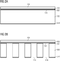
- Figure 2 shows an exemplary method of fabricating a power semiconductor device in the form of a MOSFET 220 that incorporates the different epitaxial layers and the pit structure of the present invention as already described with respect to Figure 1 .
- the layout and the fabrication of the first fabrication steps are the same as for the SiC Schottky diode 180 ( Fig. 2b and Fig. 2c ).
- the final fabrication steps, as shown in Fig. 2d instead are substantially equivalent to the MOSFET device shown e.g. in FIG. 1 of U.S. Patent Publication No. 2006/0192256 or Fig.4 of U.S. Patent
- reference signs 420 represents an N CSL epilayer
- 426, 428 represent base regions
- 430 is a JFET region
- 434 is an interface between the N CSL epilayer 424 and the P Well base regions
- 442, 444 are P+ source regions
- 446, 448 are source regions
- 446, 448 are source regions
- 450, 452 are source contacts
- 454 is a contact for a dielectric region 456.
- the presented structure can have all elements of a standard vertical silicon carbide MOSFET with the benefit of the pits 110 extending throughout all the substrate, and through the first layer 101 and the second layer 102.
- the fabrication of the "standard" vertical SiC MOSFET is well known and may be carried out as described e.g. in U.S. Patent Publication No. 2006/0192256 A1 .
- an insulated gate bipolar transistor (IGBT) having the pitted silicon carbide substrate can be realized.
- the layout and fabrication of the first fabrication steps is the same as the SiC Schottky diode 180, except that, in this case, the third layer 103 has a different doping type with respect to the second layer 102 and will act both as a back Ohmic contact "enhancer” as well as “minority carriers injector” to further reduce the R ON resistance of the power device.
- the final fabrication steps instead are substantially equivalent to e.g. the IGBT device shown in Fig.1 of U.S. Patent No. US 4,364,073 A1 .
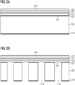
- an improved Gallium Nitride based device 320 having the pitted silicon carbide substrate to reduce switching losses and current leakage, can be realized.
- the initial structure has the silicon carbide substrate 100, a first homoepitaxial layer 101 formed on a first or upper surface, a second homoepitaxial layer 102.
- the silicon carbide substrate 100 is a highly doped n+ layer.
- the first layer 101 has the same doping type of the silicon carbide substrate 100 and the second layer 102 has the same doping type of the first layer 101 but lower concentration.
- AlN Aluminum Nitride
- GaN Gallium Nitride
- AlN Aluminum Nitride
- AlGaN Aluminum gallium nitride
- Fig.3b shows a first intermediate fabrication step which, similarly to Fig.1b , starts with the creation of pits 110, initially generated by RIE in the additional layer Lm1, if present, extending thorough the full silicon carbide substrate 100 and the first layer 101, but blocked by the etch stop layer 102.
- the pits 110 are then further extended through the second layer 102 by mean of either RIE, electrochemical, photo-electrochemical etching or a combination of them.
- Fig.3d shows the final schematic GaN HEMT structure containing source contacts 130, a gate insulator 131, a gate contact 132 and a drain contact 133.
- an improved Gallium Nitride based device 320 having the pitted silicon carbide substrate to reduce switching losses and currents leakage, can be realized.
- the Aluminum Nitride (AlN) nucleation layer 120, the Gallium Nitride (GaN) buffer layer 121, the Aluminum Nitride (AlN) barrier layer 122 and the Aluminum gallium nitride (AlGaN) cap layer 123 are epitaxially grown directly on the silicon carbide substrate 100, without any epitaxial SiC layer in between.
- This solution relies on the possibility of stopping the electrochemical etching process thanks to the holes barrier heights generated at the SiC/AlN( ⁇ 1.7eV)[iv] or SiC/GaN ( ⁇ 0.8eV)[v] heterojunctions, without the use, instead, of the SiC etch stopper layer 102.
- This solution has two important further benefits: (i) it reduces fabrication costs avoiding the need of SiC epitaxial layers and (ii) it allows using on-axis SiC substrates.
- the structure of pits could be different from what presented in Fig.3 to optimize e.g. for thermal heat dissipation through the SiC substrate while minimizing switching losses thanks to the pits distribution.
- some pits through the substrate could further extend through some or all the Nitride layers as through-wafer slot vias, to achieve monolithic integration of the microwave circuits.
- the presented structure can have all elements of a standard lateral GaN HEMT with the benefit of the pits 110 extending at least throughout all the substrate.
- the fabrication of the "standard" lateral GaN HEMT is well known and may be carried out as described e.g. in review paper [vi].
- an improved SiC based sensor is realized.
- the initial structure has the silicon carbide substrate 100, a first homoepitaxial layer 101 and at least a second homoepitaxial layer 102 formed on a first or upper surface, the embodiment can also have a homoepitaxial layer Lm1 formed on the second, or lower, surface of the silicon carbide substrate 100.
- the silicon carbide substrate 100 is a highly doped n+ layer.
- the first layer 101 has the same doping type of the substrate with, equal or higher, concentration and the second layer 102 a lower doping concentration with respect to the first layer.
- the additional layer Lm1 if present, has a lower concentration than the substrate 100.
- the second layer 102 further contains isolated point defects 140 generated either during the epitaxial growth or after growth by implantation.
- the point defects can be e.g. silicon vacancies or transition metals localized impurities and should preferentially have a distance greater than 100nm, to act as isolated spin systems.
- the second layer 102 is used both as etch stop and to enhance the optical properties of the spin system by e.g. increasing the optical emission rate due to the Purcell Effect. Since this effect increases for decreasing thicknesses of the second layer 102, layer 102 should have a thickness of less than 10 ⁇ m, preferentially less than 1 ⁇ m.
- Fig.4b shows a first intermediate fabrication step where a pattern of pits 110, initially generated by RIE in the additional layer Lm1, if present, is then extended thorough the full substrate and the layer 101 by mean of electrochemical etching. This technique allows a local selective full removal of the silicon carbide substrate 100 and the first layer 101, but it is blocked by the second etch stopper layer 102.
- the system i.e. the suspended membranes in the second layer 102, can be further processed, e.g. by realizing optical cavities around the spin-defects (see Fig.4c ) to further enhance the optical properties.
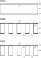
- the initial structure has a silicon carbide substrate 100, a first homoepitaxial layer 101 at least a second homoepitaxial layer 102 and an epitaxial graphene layer 153 on top of the second layer 102, all formed on a first or upper surface of the substrate, the embodiment can also have a homoepitaxial layer Lm1 formed on the second, or lower, surface of the silicon carbide substrate 100.
- the silicon carbide substrate 100 is a highly doped n+ layer.
- the first layer 101 has the same doping type of the substrate with, equal or higher, concentration.
- the second layer 102 has the same doping type of the first layer but lower concentration.
- the additional layer Lm1 if present, has a lower concentration than the SiC substrate 100.
- Fig.5b shows a first intermediate fabrication step where a pattern of pits 110, initially generated by RIE in the additional layer Lm1, if present, is then extended thorough the full substrate and the first layer 101 by mean of electrochemical etching. This technique allows a local selective full removal of the silicon carbide substrate 100 and the first layer 101, but it is blocked by the second etch stop layer 102.
- Fig.5c shows a second fabrication step where the pattern of pits 110 is further etched by photo-electrochemical etching (PECE), similarly to what was tested in ref.[vii], to selectively remove portions of the second layer 102, generating a new pit structure 111 which allow release of the graphene membrane 153.
- PECE photo-electrochemical etching
- the PECE as compared to the ECE process used to remove the silicon carbide substrate 100 and the first layer 101, has an important beneficial characteristic and a limiting one:
- the proposed Graphene/SiC multilayered structure ( Fig.5a ) and the specific consecutive combination of ECE and PECE allows for an industrially compatible transfer-less, wafer-level fabrication of free-standing graphene membranes on up to 200mm SiC substrates, as compared to the ⁇ 3mm sample used in scientific document [vii]. Furthermore, the possibility of realizing free-standing graphene membranes without transfer processes at wafer-level allows usage of standard microfabrication processes, e.g. lithographic steps and RIE, to further process the realized free-standing graphene membranes to fabricate e.g. gas, optical sensors or ultrafast transistors.
- standard microfabrication processes e.g. lithographic steps and RIE
Landscapes
- Junction Field-Effect Transistors (AREA)
- Physics & Mathematics (AREA)
- Engineering & Computer Science (AREA)
- Plasma & Fusion (AREA)
- Chemical & Material Sciences (AREA)
- Crystallography & Structural Chemistry (AREA)
- Electrodes Of Semiconductors (AREA)
Priority Applications (4)
| Application Number | Priority Date | Filing Date | Title |
|---|---|---|---|
| EP19208585.0A EP3823008A1 (de) | 2019-11-12 | 2019-11-12 | Verfahren zur herstellung von halbleiterbauelementen |
| EP20816093.7A EP4059046A1 (de) | 2019-11-12 | 2020-11-05 | Verfahren zur herstellung von halbleiterbauelementen |
| US17/776,311 US12278270B2 (en) | 2019-11-12 | 2020-11-05 | Methods of manufacturing semiconductor devices |
| PCT/EP2020/081051 WO2021094176A1 (en) | 2019-11-12 | 2020-11-05 | Methods of manufacturing semiconductor devices |
Applications Claiming Priority (1)
| Application Number | Priority Date | Filing Date | Title |
|---|---|---|---|
| EP19208585.0A EP3823008A1 (de) | 2019-11-12 | 2019-11-12 | Verfahren zur herstellung von halbleiterbauelementen |
Publications (1)
| Publication Number | Publication Date |
|---|---|
| EP3823008A1 true EP3823008A1 (de) | 2021-05-19 |
Family
ID=68583067
Family Applications (2)
| Application Number | Title | Priority Date | Filing Date |
|---|---|---|---|
| EP19208585.0A Withdrawn EP3823008A1 (de) | 2019-11-12 | 2019-11-12 | Verfahren zur herstellung von halbleiterbauelementen |
| EP20816093.7A Pending EP4059046A1 (de) | 2019-11-12 | 2020-11-05 | Verfahren zur herstellung von halbleiterbauelementen |
Family Applications After (1)
| Application Number | Title | Priority Date | Filing Date |
|---|---|---|---|
| EP20816093.7A Pending EP4059046A1 (de) | 2019-11-12 | 2020-11-05 | Verfahren zur herstellung von halbleiterbauelementen |
Country Status (3)
| Country | Link |
|---|---|
| US (1) | US12278270B2 (de) |
| EP (2) | EP3823008A1 (de) |
| WO (1) | WO2021094176A1 (de) |
Cited By (1)
| Publication number | Priority date | Publication date | Assignee | Title |
|---|---|---|---|---|
| IT202300010203A1 (it) | 2023-05-19 | 2024-11-19 | Consiglio Nazionale Ricerche | Un transistor di potenza per un dispositivo a semiconduttore |
Families Citing this family (3)
| Publication number | Priority date | Publication date | Assignee | Title |
|---|---|---|---|---|
| CN115985888B (zh) * | 2023-02-23 | 2024-07-05 | 天津大学 | 一种由电容耦合互联得到的集成垂直器件及其制备方法 |
| CN115863399A (zh) * | 2023-02-24 | 2023-03-28 | 成都功成半导体有限公司 | 一种在金刚石衬底上键合GaN层的方法及其器件 |
| EP4439632A1 (de) * | 2023-03-27 | 2024-10-02 | Hitachi Energy Ltd | Halbleitervorrichtung und herstellungsverfahren dafür |
Citations (6)
| Publication number | Priority date | Publication date | Assignee | Title |
|---|---|---|---|---|
| US4364073A (en) | 1980-03-25 | 1982-12-14 | Rca Corporation | Power MOSFET with an anode region |
| US6306773B1 (en) * | 2000-02-01 | 2001-10-23 | Adaas Christian | Method of producing a semiconductor device of SiC |
| US6884740B2 (en) | 2001-09-04 | 2005-04-26 | The Regents Of The University Of California | Photoelectrochemical undercut etching of semiconductor material |
| US20060192256A1 (en) | 2005-01-21 | 2006-08-31 | Cooper James A | High-voltage power semiconductor device |
| US20070200116A1 (en) * | 2006-01-10 | 2007-08-30 | Christopher Harris | Silicon carbide dimpled substrate |
| US20170025530A1 (en) | 2015-02-27 | 2017-01-26 | Purdue Research Foundation | METHODS OF REDUCING THE ELECTRICAL AND THERMAL RESISTANCE OF SiC SUBSTRATES AND DEVICES MADE THEREBY |
Family Cites Families (6)
| Publication number | Priority date | Publication date | Assignee | Title |
|---|---|---|---|---|
| KR100192549B1 (ko) * | 1996-07-31 | 1999-06-15 | 구본준 | 마스크의 구조 및 제조방법 |
| US7541640B2 (en) * | 2006-06-21 | 2009-06-02 | Flextronics International Usa, Inc. | Vertical field-effect transistor and method of forming the same |
| US9166048B2 (en) * | 2012-09-16 | 2015-10-20 | Sensor Electronic Technology, Inc. | Lateral/vertical semiconductor device |
| US9656859B2 (en) * | 2015-04-16 | 2017-05-23 | The United States Of America, As Represented By The Secretary Of The Navy | Method for fabricating suspended MEMS structures |
| US10985285B2 (en) * | 2016-08-17 | 2021-04-20 | The Regents Of The University Of California | Methods for fabricating III-nitride tunnel junction devices |
| US11411099B2 (en) * | 2019-05-28 | 2022-08-09 | Glc Semiconductor Group (Cq) Co., Ltd. | Semiconductor device |
-
2019
- 2019-11-12 EP EP19208585.0A patent/EP3823008A1/de not_active Withdrawn
-
2020
- 2020-11-05 EP EP20816093.7A patent/EP4059046A1/de active Pending
- 2020-11-05 WO PCT/EP2020/081051 patent/WO2021094176A1/en not_active Ceased
- 2020-11-05 US US17/776,311 patent/US12278270B2/en active Active
Patent Citations (6)
| Publication number | Priority date | Publication date | Assignee | Title |
|---|---|---|---|---|
| US4364073A (en) | 1980-03-25 | 1982-12-14 | Rca Corporation | Power MOSFET with an anode region |
| US6306773B1 (en) * | 2000-02-01 | 2001-10-23 | Adaas Christian | Method of producing a semiconductor device of SiC |
| US6884740B2 (en) | 2001-09-04 | 2005-04-26 | The Regents Of The University Of California | Photoelectrochemical undercut etching of semiconductor material |
| US20060192256A1 (en) | 2005-01-21 | 2006-08-31 | Cooper James A | High-voltage power semiconductor device |
| US20070200116A1 (en) * | 2006-01-10 | 2007-08-30 | Christopher Harris | Silicon carbide dimpled substrate |
| US20170025530A1 (en) | 2015-02-27 | 2017-01-26 | Purdue Research Foundation | METHODS OF REDUCING THE ELECTRICAL AND THERMAL RESISTANCE OF SiC SUBSTRATES AND DEVICES MADE THEREBY |
Non-Patent Citations (8)
| Title |
|---|
| D. WALDMANNB. BUTZS. BAUERJ. M. ENGLERTJ. JOBSTK. ULLMANNF. FROMMM. AMMONM. ENZELBERGERA. HIRSCH: "Robust Graphene Membranes in a Silicon Carbide Frame", ACS NANO, vol. 7, 2013, pages 4441 |
| J. CHOIR. PUTHENKOVILAKAMJ. P. CHANG, APPL. PHYS. LETT., vol. 86, 2005, pages 192101 |
| M. KOKAL: "AIGaN/GaN MBE 2DEG Heterostructures: Interplay between Surface-, Interfaceand Device-Properties", PHD. DISSERTATION, 2003 |
| N.PILUSOA. SEVERINOR. ANZALONEM.A. DI STEFANOE. FONTANAM. SALANITRIS. LORENTIA. CAMPIONEP. FIORENZAF. LA VIA: "Growth of 4H-SiC Epitaxial Layer through Optimization of Buffer Layer", MATERIAL SCIENCE FORUM, vol. 924, 2018, pages 84 |
| R. S. PENGELLYS. M. WOODJ. W. MILLIGANS. T. SHEPPARDL. PRIBBLE, IEEE TRANSACTIONS ON MICROWAVE THEORY AND TECHNIQUES, vol. 6, 2012 |
| RAJENDRA DAHAL ET AL: "Fabrication of Thick Free-Standing Lightly-Doped n-Type 4H-SiC Wafers", MATERIALS SCIENCE FORUM, vol. 897, 15 May 2017 (2017-05-15), pages 379 - 382, XP055500219, DOI: 10.4028/www.scientific.net/MSF.897.379 * |
| SHOR J S ET AL: "Dopant-selective etch stops in 6H and 3C SiC", JOURNAL OF APPLIED PHYSICS, AMERICAN INSTITUTE OF PHYSICS, US, vol. 81, no. 3, 1 February 1997 (1997-02-01), pages 1546, XP012041542, ISSN: 0021-8979, DOI: 10.1063/1.363890 * |
| T. TAWARAT. MIYAZAWAM. RYOM. MIYAZATOT. FUJIMOTOK. TAKENAKAS. MATSUNAGAM. MIYAJIMAA. OTSUKIY. YONEZAWA: "Suppression of the Forward Degradation in 4H-SiC PiN Diodes by Employing a Recombination-Enhanced Buffer Layer", MATERIAL SCIENCE FORUM, vol. 897, 2017, pages 419 |
Cited By (2)
| Publication number | Priority date | Publication date | Assignee | Title |
|---|---|---|---|---|
| IT202300010203A1 (it) | 2023-05-19 | 2024-11-19 | Consiglio Nazionale Ricerche | Un transistor di potenza per un dispositivo a semiconduttore |
| WO2024241167A1 (en) | 2023-05-19 | 2024-11-28 | Consiglio Nazionale Delle Ricerche | Power transistor semiconductor device and method therefor |
Also Published As
| Publication number | Publication date |
|---|---|
| US12278270B2 (en) | 2025-04-15 |
| US20220399442A1 (en) | 2022-12-15 |
| EP4059046A1 (de) | 2022-09-21 |
| WO2021094176A1 (en) | 2021-05-20 |
Similar Documents
| Publication | Publication Date | Title |
|---|---|---|
| US12142674B2 (en) | Gallium Nitride high-electron mobility transistors with p-type layers and process for making the same | |
| Hu et al. | Materials and processing issues in vertical GaN power electronics | |
| US12278270B2 (en) | Methods of manufacturing semiconductor devices | |
| CN109037323B (zh) | 具有选择性生成的2deg沟道的常关型hemt晶体管及其制造方法 | |
| JP7009401B2 (ja) | シリコンカーバイド基板に深く注入されたp-型層を有する窒化ガリウム高電子移動度トランジスタ | |
| US20060226412A1 (en) | Thick semi-insulating or insulating epitaxial gallium nitride layers and devices incorporating same | |
| KR102813619B1 (ko) | 수직형 hemt 및 수직형 hemt 제조 방법 | |
| US10840334B2 (en) | Gallium nitride high-electron mobility transistors with deep implanted p-type layers in silicon carbide substrates for power switching and radio frequency applications and process for making the same | |
| CN112133761B (zh) | 一种基于GaN的横向结势垒肖特基二极管及其制备方法 | |
| WO2006093174A1 (ja) | 縦型窒化ガリウム半導体装置およびエピタキシャル基板 | |
| KR20150084855A (ko) | 이중 금속의 부분 리세스된 전극을 갖는 GaN계 쇼트키 다이오드 | |
| JP2022519825A (ja) | 埋込みp型層を有する第III族窒化物高電子移動度トランジスタおよびその作製プロセス | |
| KR20140124273A (ko) | 질화물 반도체 소자 및 그 제조 방법 | |
| US8569153B2 (en) | Method and system for carbon doping control in gallium nitride based devices | |
| WO2006031654A2 (en) | Hemt device and method of making | |
| KR101148694B1 (ko) | 질화물계 반도체 소자 및 그 제조 방법 | |
| CN114335145A (zh) | 一种抑制电流崩塌的hemt器件及其生产方法 | |
| KR100768803B1 (ko) | Ⅲ-ⅴ족 화합물층을 구비한 반도체 소자 | |
| JP4850423B2 (ja) | 窒化物半導体装置 | |
| JP2010177416A (ja) | 窒化物半導体装置 | |
| CN114335192A (zh) | 快速恢复二极管及其制造方法 | |
| US20240347629A1 (en) | High-power component based on iii nitride compound semiconductors, intermediate product and process for production of a high-power component | |
| CN113990920B (zh) | 一种具有壳核结构的氮化物功率半导体器件及其制备方法 | |
| CN113826212A (zh) | 一种半导体结构的制备方法 | |
| JP2008258310A (ja) | 窒化物半導体装置 |
Legal Events
| Date | Code | Title | Description |
|---|---|---|---|
| PUAI | Public reference made under article 153(3) epc to a published international application that has entered the european phase |
Free format text: ORIGINAL CODE: 0009012 |
|
| STAA | Information on the status of an ep patent application or granted ep patent |
Free format text: STATUS: THE APPLICATION HAS BEEN PUBLISHED |
|
| AK | Designated contracting states |
Kind code of ref document: A1 Designated state(s): AL AT BE BG CH CY CZ DE DK EE ES FI FR GB GR HR HU IE IS IT LI LT LU LV MC MK MT NL NO PL PT RO RS SE SI SK SM TR |
|
| STAA | Information on the status of an ep patent application or granted ep patent |
Free format text: STATUS: THE APPLICATION IS DEEMED TO BE WITHDRAWN |
|
| 18D | Application deemed to be withdrawn |
Effective date: 20211120 |