EP3828626B1 - Anzeigevorrichtung - Google Patents
Anzeigevorrichtung Download PDFInfo
- Publication number
- EP3828626B1 EP3828626B1 EP19849494.0A EP19849494A EP3828626B1 EP 3828626 B1 EP3828626 B1 EP 3828626B1 EP 19849494 A EP19849494 A EP 19849494A EP 3828626 B1 EP3828626 B1 EP 3828626B1
- Authority
- EP
- European Patent Office
- Prior art keywords
- substrate
- disposed
- display device
- recessed portion
- region
- Prior art date
- Legal status (The legal status is an assumption and is not a legal conclusion. Google has not performed a legal analysis and makes no representation as to the accuracy of the status listed.)
- Active
Links
Images












Classifications
-
- G—PHYSICS
- G02—OPTICS
- G02F—OPTICAL DEVICES OR ARRANGEMENTS FOR THE CONTROL OF LIGHT BY MODIFICATION OF THE OPTICAL PROPERTIES OF THE MEDIA OF THE ELEMENTS INVOLVED THEREIN; NON-LINEAR OPTICS; FREQUENCY-CHANGING OF LIGHT; OPTICAL LOGIC ELEMENTS; OPTICAL ANALOGUE/DIGITAL CONVERTERS
- G02F1/00—Devices or arrangements for the control of the intensity, colour, phase, polarisation or direction of light arriving from an independent light source, e.g. switching, gating or modulating; Non-linear optics
- G02F1/01—Devices or arrangements for the control of the intensity, colour, phase, polarisation or direction of light arriving from an independent light source, e.g. switching, gating or modulating; Non-linear optics for the control of the intensity, phase, polarisation or colour
- G02F1/13—Devices or arrangements for the control of the intensity, colour, phase, polarisation or direction of light arriving from an independent light source, e.g. switching, gating or modulating; Non-linear optics for the control of the intensity, phase, polarisation or colour based on liquid crystals, e.g. single liquid crystal display cells
- G02F1/133—Constructional arrangements; Operation of liquid crystal cells; Circuit arrangements
- G02F1/1333—Constructional arrangements; Manufacturing methods
- G02F1/1345—Conductors connecting electrodes to cell terminals
-
- G—PHYSICS
- G02—OPTICS
- G02F—OPTICAL DEVICES OR ARRANGEMENTS FOR THE CONTROL OF LIGHT BY MODIFICATION OF THE OPTICAL PROPERTIES OF THE MEDIA OF THE ELEMENTS INVOLVED THEREIN; NON-LINEAR OPTICS; FREQUENCY-CHANGING OF LIGHT; OPTICAL LOGIC ELEMENTS; OPTICAL ANALOGUE/DIGITAL CONVERTERS
- G02F1/00—Devices or arrangements for the control of the intensity, colour, phase, polarisation or direction of light arriving from an independent light source, e.g. switching, gating or modulating; Non-linear optics
- G02F1/01—Devices or arrangements for the control of the intensity, colour, phase, polarisation or direction of light arriving from an independent light source, e.g. switching, gating or modulating; Non-linear optics for the control of the intensity, phase, polarisation or colour
- G02F1/13—Devices or arrangements for the control of the intensity, colour, phase, polarisation or direction of light arriving from an independent light source, e.g. switching, gating or modulating; Non-linear optics for the control of the intensity, phase, polarisation or colour based on liquid crystals, e.g. single liquid crystal display cells
- G02F1/133—Constructional arrangements; Operation of liquid crystal cells; Circuit arrangements
- G02F1/1333—Constructional arrangements; Manufacturing methods
- G02F1/1345—Conductors connecting electrodes to cell terminals
- G02F1/13452—Conductors connecting driver circuitry and terminals of panels
-
- G—PHYSICS
- G02—OPTICS
- G02F—OPTICAL DEVICES OR ARRANGEMENTS FOR THE CONTROL OF LIGHT BY MODIFICATION OF THE OPTICAL PROPERTIES OF THE MEDIA OF THE ELEMENTS INVOLVED THEREIN; NON-LINEAR OPTICS; FREQUENCY-CHANGING OF LIGHT; OPTICAL LOGIC ELEMENTS; OPTICAL ANALOGUE/DIGITAL CONVERTERS
- G02F1/00—Devices or arrangements for the control of the intensity, colour, phase, polarisation or direction of light arriving from an independent light source, e.g. switching, gating or modulating; Non-linear optics
- G02F1/01—Devices or arrangements for the control of the intensity, colour, phase, polarisation or direction of light arriving from an independent light source, e.g. switching, gating or modulating; Non-linear optics for the control of the intensity, phase, polarisation or colour
- G02F1/13—Devices or arrangements for the control of the intensity, colour, phase, polarisation or direction of light arriving from an independent light source, e.g. switching, gating or modulating; Non-linear optics for the control of the intensity, phase, polarisation or colour based on liquid crystals, e.g. single liquid crystal display cells
- G02F1/133—Constructional arrangements; Operation of liquid crystal cells; Circuit arrangements
- G02F1/1333—Constructional arrangements; Manufacturing methods
- G02F1/133302—Rigid substrates, e.g. inorganic substrates
-
- G—PHYSICS
- G02—OPTICS
- G02F—OPTICAL DEVICES OR ARRANGEMENTS FOR THE CONTROL OF LIGHT BY MODIFICATION OF THE OPTICAL PROPERTIES OF THE MEDIA OF THE ELEMENTS INVOLVED THEREIN; NON-LINEAR OPTICS; FREQUENCY-CHANGING OF LIGHT; OPTICAL LOGIC ELEMENTS; OPTICAL ANALOGUE/DIGITAL CONVERTERS
- G02F1/00—Devices or arrangements for the control of the intensity, colour, phase, polarisation or direction of light arriving from an independent light source, e.g. switching, gating or modulating; Non-linear optics
- G02F1/01—Devices or arrangements for the control of the intensity, colour, phase, polarisation or direction of light arriving from an independent light source, e.g. switching, gating or modulating; Non-linear optics for the control of the intensity, phase, polarisation or colour
- G02F1/13—Devices or arrangements for the control of the intensity, colour, phase, polarisation or direction of light arriving from an independent light source, e.g. switching, gating or modulating; Non-linear optics for the control of the intensity, phase, polarisation or colour based on liquid crystals, e.g. single liquid crystal display cells
- G02F1/133—Constructional arrangements; Operation of liquid crystal cells; Circuit arrangements
- G02F1/1333—Constructional arrangements; Manufacturing methods
- G02F1/1339—Gaskets; Spacers; Sealing of cells
-
- H—ELECTRICITY
- H05—ELECTRIC TECHNIQUES NOT OTHERWISE PROVIDED FOR
- H05K—PRINTED CIRCUITS; CASINGS OR CONSTRUCTIONAL DETAILS OF ELECTRIC APPARATUS; MANUFACTURE OF ASSEMBLAGES OF ELECTRICAL COMPONENTS
- H05K1/00—Printed circuits
- H05K1/02—Details
- H05K1/11—Printed elements for providing electric connections to or between printed circuits
- H05K1/118—Printed elements for providing electric connections to or between printed circuits specially for flexible printed circuits, e.g. using folded portions
-
- H—ELECTRICITY
- H05—ELECTRIC TECHNIQUES NOT OTHERWISE PROVIDED FOR
- H05K—PRINTED CIRCUITS; CASINGS OR CONSTRUCTIONAL DETAILS OF ELECTRIC APPARATUS; MANUFACTURE OF ASSEMBLAGES OF ELECTRICAL COMPONENTS
- H05K1/00—Printed circuits
- H05K1/02—Details
- H05K1/14—Structural association of two or more printed circuits
- H05K1/147—Structural association of two or more printed circuits at least one of the printed circuits being bent or folded, e.g. by using a flexible printed circuit
-
- H—ELECTRICITY
- H10—SEMICONDUCTOR DEVICES; ELECTRIC SOLID-STATE DEVICES NOT OTHERWISE PROVIDED FOR
- H10K—ORGANIC ELECTRIC SOLID-STATE DEVICES
- H10K59/00—Integrated devices, or assemblies of multiple devices, comprising at least one organic light-emitting element covered by group H10K50/00
- H10K59/10—OLED displays
- H10K59/12—Active-matrix OLED [AMOLED] displays
- H10K59/131—Interconnections, e.g. wiring lines or terminals
-
- G—PHYSICS
- G02—OPTICS
- G02F—OPTICAL DEVICES OR ARRANGEMENTS FOR THE CONTROL OF LIGHT BY MODIFICATION OF THE OPTICAL PROPERTIES OF THE MEDIA OF THE ELEMENTS INVOLVED THEREIN; NON-LINEAR OPTICS; FREQUENCY-CHANGING OF LIGHT; OPTICAL LOGIC ELEMENTS; OPTICAL ANALOGUE/DIGITAL CONVERTERS
- G02F1/00—Devices or arrangements for the control of the intensity, colour, phase, polarisation or direction of light arriving from an independent light source, e.g. switching, gating or modulating; Non-linear optics
- G02F1/01—Devices or arrangements for the control of the intensity, colour, phase, polarisation or direction of light arriving from an independent light source, e.g. switching, gating or modulating; Non-linear optics for the control of the intensity, phase, polarisation or colour
- G02F1/13—Devices or arrangements for the control of the intensity, colour, phase, polarisation or direction of light arriving from an independent light source, e.g. switching, gating or modulating; Non-linear optics for the control of the intensity, phase, polarisation or colour based on liquid crystals, e.g. single liquid crystal display cells
- G02F1/1303—Apparatus specially adapted to the manufacture of LCDs
-
- G—PHYSICS
- G02—OPTICS
- G02F—OPTICAL DEVICES OR ARRANGEMENTS FOR THE CONTROL OF LIGHT BY MODIFICATION OF THE OPTICAL PROPERTIES OF THE MEDIA OF THE ELEMENTS INVOLVED THEREIN; NON-LINEAR OPTICS; FREQUENCY-CHANGING OF LIGHT; OPTICAL LOGIC ELEMENTS; OPTICAL ANALOGUE/DIGITAL CONVERTERS
- G02F1/00—Devices or arrangements for the control of the intensity, colour, phase, polarisation or direction of light arriving from an independent light source, e.g. switching, gating or modulating; Non-linear optics
- G02F1/01—Devices or arrangements for the control of the intensity, colour, phase, polarisation or direction of light arriving from an independent light source, e.g. switching, gating or modulating; Non-linear optics for the control of the intensity, phase, polarisation or colour
- G02F1/13—Devices or arrangements for the control of the intensity, colour, phase, polarisation or direction of light arriving from an independent light source, e.g. switching, gating or modulating; Non-linear optics for the control of the intensity, phase, polarisation or colour based on liquid crystals, e.g. single liquid crystal display cells
- G02F1/133—Constructional arrangements; Operation of liquid crystal cells; Circuit arrangements
- G02F1/1333—Constructional arrangements; Manufacturing methods
- G02F1/13336—Combining plural substrates to produce large-area displays, e.g. tiled displays
-
- H—ELECTRICITY
- H05—ELECTRIC TECHNIQUES NOT OTHERWISE PROVIDED FOR
- H05K—PRINTED CIRCUITS; CASINGS OR CONSTRUCTIONAL DETAILS OF ELECTRIC APPARATUS; MANUFACTURE OF ASSEMBLAGES OF ELECTRICAL COMPONENTS
- H05K2201/00—Indexing scheme relating to printed circuits covered by H05K1/00
- H05K2201/03—Conductive materials
- H05K2201/0332—Structure of the conductor
- H05K2201/0364—Conductor shape
- H05K2201/0367—Metallic bump or raised conductor not used as solder bump
-
- H—ELECTRICITY
- H05—ELECTRIC TECHNIQUES NOT OTHERWISE PROVIDED FOR
- H05K—PRINTED CIRCUITS; CASINGS OR CONSTRUCTIONAL DETAILS OF ELECTRIC APPARATUS; MANUFACTURE OF ASSEMBLAGES OF ELECTRICAL COMPONENTS
- H05K2201/00—Indexing scheme relating to printed circuits covered by H05K1/00
- H05K2201/05—Flexible printed circuits [FPCs]
-
- H—ELECTRICITY
- H05—ELECTRIC TECHNIQUES NOT OTHERWISE PROVIDED FOR
- H05K—PRINTED CIRCUITS; CASINGS OR CONSTRUCTIONAL DETAILS OF ELECTRIC APPARATUS; MANUFACTURE OF ASSEMBLAGES OF ELECTRICAL COMPONENTS
- H05K2201/00—Indexing scheme relating to printed circuits covered by H05K1/00
- H05K2201/09—Shape and layout
- H05K2201/09145—Edge details
- H05K2201/09163—Slotted edge
-
- H—ELECTRICITY
- H05—ELECTRIC TECHNIQUES NOT OTHERWISE PROVIDED FOR
- H05K—PRINTED CIRCUITS; CASINGS OR CONSTRUCTIONAL DETAILS OF ELECTRIC APPARATUS; MANUFACTURE OF ASSEMBLAGES OF ELECTRICAL COMPONENTS
- H05K2201/00—Indexing scheme relating to printed circuits covered by H05K1/00
- H05K2201/10—Details of components or other objects attached to or integrated in a printed circuit board
- H05K2201/10007—Types of components
- H05K2201/10128—Display
Definitions
- the present invention relates to a display device and a method of manufacturing the same.
- LCDs liquid crystal display devices
- OLED organic light-emitting diode
- An area in which drive integrated circuits (ICs) or other printed circuits are installed is present in a periphery of a glass substrate constituting the display device, and this area may be a non-display area in which an image is not displayed and referred to as a bezel.
- ICs drive integrated circuits
- this area may be a non-display area in which an image is not displayed and referred to as a bezel.
- US 2017/358602 A1 discloses a display apparatus in which a connection pad is coupled to side surfaces of the substrates and extends between the substrates.
- the present invention is directed to providing a display device and a method of manufacturing the same, which reduce a bezel area and prevent a connection line and a line layer from being open.
- a bezel area in a display device, can be effectively reduced and a connection line and a line layer can be prevented from being open.
- first, second, and the like are used to describe various components, these components are substantially not limited by these terms. These terms are used only to distinguish one component from another component. Therefore, a first component described below may substantially be a second component within the technical spirit of the present invention.
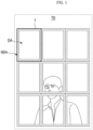
- FIG. 1 is a schematic diagram illustrating a tile-type display device
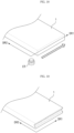
- FIG. 2 is a perspective view illustrating a display device according to one embodiment
- FIG. 3 is an exploded perspective view illustrating some parts of the display device of FIG. 1 which are disassembled
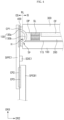
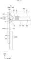
- FIG. 4 is a cross-sectional view taken along line A-A' of FIG. 2
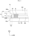
- FIG. 5 is a schematic cross-sectional view illustrating a portion of FIG. 4 to describe a recessed portion.
- a display device is a liquid crystal display device including a liquid crystal layer
- the present invention is not limited thereto.
- a display device e.g., an organic light-emitting diode display device
- some components which will be described below, may be omitted or other components not described here may be added.
- the display device may be applied to large electronic equipment such as televisions or external advertising boards and small-to-medium-sized electronic equipment such as personal computers (PCs), laptop computers, vehicle navigation units, and cameras.
- the display device may be applied to tablet PCs, smart phones, personal digital assistants (PDAs), portable multimedia players (PMPs), game machines, and wristwatch type electronic devices.
- PDAs personal digital assistants
- PMPs portable multimedia players
- game machines and wristwatch type electronic devices.
- wristwatch type electronic devices The above electronic devices are merely illustrative, and other electronic devices may also be employed.
- a tile type display TD may include a plurality of display devices 1.
- the plurality of display devices 1 may be arranged in a grid shape, but the present invention is not limited thereto, and the plurality of display devices 1 may be arranged in the form of being connected in a first direction, connected in a second direction, and connected to have a specific shape.
- the plurality of display devices may be the same size, but the present invention is not limited thereto, and the plurality of display devices may be different sizes.
- each of the plurality of display devices 1 included in the tile type display TD may be a rectangular shape including a long side and a short side.
- the plurality of display devices 1 may be disposed such that long sides or short sides are connected to each other.
- some of the display devices 1 may form one side of the tile type display TD, and some of the display devices 1 are located at a corner of the tile type display TD to form two adjacent sides of the tile type display TD, and some of the display devices 1 may form a structure which is located inside the tile type display TD to be surrounded by other display devices 1.
- the plurality of display devices 1 may have different bezel shapes according to their positions and may have the same bezel shape.
- the tile type display TD may be a flat display device 1, but the present invention is not limited thereto, and the tile type display TD may have a three-dimensional shape so as to provide a three-dimensional effect.
- each of the display devices 1 included in the tile type display TD may have a curved shape and may be connected with a flat shape or a predetermined angle to three-dimensionally form an entire shape of the tile type display TD.
- Bezels of the plurality of display devices 1 may be connected to be in contact with each other or connected through a connection member (not shown). As described above, since the plurality of display devices 1 are connected in the tile type display TD, bezel areas of the display devices 1 are disposed to overlap in a connection portion so that each of the display devices 1 is required to have a thin bezel, and to this end, each of the display devices 1 may be equipped with a side connection pad. A detailed description thereof will be described below.
- each of the display devices 1 may include a first substrate 100, a liquid crystal layer 200, and a second substrate 300.
- the display device 1 may further include a flexible printed circuit board SFPC1, a driving printed circuit board SPCB1, and a backlight unit BLU.
- each of the first substrate 100, the second substrate 300, and the backlight unit BLU may have a rectangular shape having long sides in a first direction DR1 and short sides in a second direction DR2 intersecting the first direction DR1.
- the shapes of the first substrate 100, the second substrate 300, and the backlight unit BLU are not limited thereto, and each of the first substrate 100, the second substrate 300, and the backlight unit BLU may have a curved portion in some regions, as necessary.
- the backlight unit BLU may generate light and provide the generated light to the first substrate 100, the liquid crystal layer 200, and the second substrate 300.
- a display panel including the first substrate 100, the liquid crystal layer 200, and the second substrate 300 may generate an image using the light provided from the backlight unit BLU and provide the image to the outside.
- the display panel may include a display area DA in which an image is displayed and a non-display area NDA in which an image is not displayed.
- the non-display area NDA may be an area surrounding the display area DA.
- the display device 1 may further include a window member, which covers the display panel and transmits an image to the outside, on the second substrate 300.
- the backlight unit BLU may be an edge type backlight unit or a direct type backlight unit, but the embodiments are not limited thereto.
- the first substrate 100 may include a plurality of pixels SPX.
- the plurality of pixels SPX may be arranged in the form of a matrix, but the present invention is not limited thereto.
- a plurality of gate lines SGL1 to SGLm (m is a natural number) and a plurality of data lines SDL1 to SDLn (n is a natural number) may be disposed along boundaries of the pixels SPX.
- the plurality of gate lines SGL1 to SGLm may serve as selection lines for selecting the plurality of pixels SPX.
- the plurality of pixels SPX may be substantially defined in the first substrate 100.
- a pixel electrode defining a pixel may be disposed on each of the pixels SPX.
- the gate lines SGL1 to SGLm and the data lines SDL1 to SDLn may be disposed to intersect each other and to be insulated from each other.
- the gate lines SGL1 to SGLm may extend in the first direction DR1 to be electrically connected to a gate driver SGD.
- the data lines SDL1 to SDLn may extend in the second direction DR2 to be connected to a data driver SDD.
- the pixels SPX may be disposed to be electrically connected to the gate lines SGL1 to SGLm and the data lines SDL1 to SDLn which intersect each other.
- the pixels SPX may be disposed in the form of a matrix, but the embodiments are not limited thereto.
- the gate driver SGD may be disposed in a predetermined area adjacent to at least one of the short sides of the first substrate 100.
- an arrangement position of the gate driver SGD is not limited thereto.
- the gate driver SGD may be simultaneously formed in a process of manufacturing transistors which drive the pixels SPX and mounted on the first substrate 100 in the form of an amorphous silicon thin film transistor (TFT) gate driver circuit (ASG) or an oxide silicon TFT gate driver circuit (OSG).
- TFT amorphous silicon thin film transistor
- ASG amorphous silicon thin film transistor
- OSG oxide silicon TFT gate driver circuit
- the embodiments are not limited thereto, and the gate driver SGD may be formed as a plurality of driving chips, mounted on a flexible driving circuit board, and connected to the first substrate 100 in a tape carrier package (TCP) method.
- the gate driver SGD may be formed as a plurality of driving chips and mounted on the first substrate 100 in a chip on glass (COG) method.
- the data driver SDD may include a source driving chip SDIC1.
- the data driver SDD may include one source driving chip SDIC 1 or a plurality of source driving chips SDIC1. In the embodiment shown in the drawings, an example in which five source driving chips SDIC1 are disposed will be described, but it is obvious that the number of the source driving chips SDIC1 is not limited.
- the driving printed circuit board SPCB 1 may include a timing controller (not shown).
- the timing controller may be mounted on the driving printed circuit board SPCB 1 in the form of an integrated circuit (IC) chip and electrically connected to the gate driver SGD and the data driver SDD.
- the timing controller may output a gate control signal, a data control signal, and pieces of image data.
- the gate driver SGD may receive a gate control signal from the timing controller. In response to a gate control signal, the gate driver SGD may generate gate signals and sequentially output the generated gate signals.
- the gate signals may be provided to the pixels PX through the gate lines SGL1 to SGLm in row units. Consequently, the pixels SPX may be driven in row units.
- the data driver SDD may receive pieces of image data and a data control signal from the timing controller. In response to the data control signal, the data driver SDD may generate and output data voltages, in the form of an analog, corresponding to the pieces of image data. The data voltages may be provided to the pixels SPX through the data lines SDL1 to SDLn.
- the pixels SPX may receive the data voltages through the data lines SDL1 to SDLn.
- the pixels SPX may display gray scales corresponding to the data voltages to control transmittance of an area in which each of the pixels SPX is disposed.
- the flexible printed circuit boards SFPC 1 have been illustrated as being connected adjacent to the long sides of the first and second substrates 100 and 300 in the drawings, the embodiments are not limited thereto. A position where the first and second substrates 100 and 300 and the flexible printed circuit board SFPC1 are connected may be changed as necessary.
- the flexible printed circuit boards SFPC1 may be disposed adjacent to the short sides of the first and second substrates 100 and 300.
- the flexible printed circuit boards SFPC1 may be disposed on the long sides of the first and second substrates 100 and 300.
- the flexible printed circuit boards SFPC1 may be disposed on the short sides of the first and second substrates 100 and 300 or may have a structure of being disposed on the long sides and short sides.
- the flexible printed circuit boards SFPC1 may include contact pads CP1.
- the source driving chips SDIC1 may be electrically connected to the contact pads CP1 of the flexible printed circuit boards SFPC1.
- the contact pads CP1 of the flexible printed circuit boards SFPC1 may be electrically connected to connection pads 130 disposed on side surfaces of the first and second substrates 100 and 300 through adhesive films 400.
- connection pads 130 may be bonded to the flexible printed circuit boards SFPC1 through the adhesive films 400.
- the connection pads 130 may be electrically connected to the contact pads CP1 of the flexible printed circuit boards SFPC1 by an outer lead bonding (OLB) method using the adhesive films 400.
- OLB outer lead bonding
- the adhesive film 400 may be disposed to entirely cover the connection pad 130, but the present invention is not limited thereto, and the adhesive film 400 may be disposed to expose a portion of the connection pad 130.
- the adhesive film 400 may include an anisotropic conductive film (ACF).
- ACF anisotropic conductive film
- the adhesive film 400 has conductivity only in an area where the connection pad 130 and the contact pad CP1 of the flexible printed circuit board SFPC1 are in contact with each other so that the connection pad 130 may be electrically connected to the contact pad CP1 of the flexible printed circuit board SFPC1.
- the connection pads 130 and the contact pads CP1 may be in direct contact with each other without the adhesive films 400 to be electrically connected.
- the connection pads 130 and the contact pads CP1 may be directly connected by an ultrasonic bonding method or a welding method.
- connection pads 130 may be electrically connected to connection lines 115 disposed on the first substrate 100.
- connection lines 115 may extend from the side surface of the first substrate 100 toward an inside thereof (e.g., extend in the second direction DR2) to be electrically connected to the plurality of pixels SPX.
- At least one side surface S1 of the display device 1 on which the connection pads 130 are disposed may include a flat portion FP and a recessed portion TP.
- a structure in which the recessed portion TP is disposed on a side surface adjacent to the long side of the display device 1 is illustrated, but the present invention is not limited thereto, and the recessed portion TP may be disposed on a side surface adjacent to the short side of the display device 1.
- the recessed portion TP may be disposed on each side surface adjacent to the long side of the display device 1.
- the recessed portion TP may have a structure of being disposed on each side surface adjacent to the short side of the display device 1 or have a structure of being disposed on a side surface adjacent to the long side and a side surface adjacent to the short side.
- the flat portion FP may serve as a buffer to prevent damage of the first substrate 100 in which the recessed portion TP is disposed and the side surface of the second substrate 300 due to an external impact.
- the recessed portion TP may be formed in a direction from the flat portion FP of the one side surface S1 of the display device 1 toward a central portion of the display device 1, for example, in the second direction DR2.
- outer surfaces 100a and 300a maximally protruding from the first substrate 100 and the second substrate 300 may be arranged in the third direction DR3 when viewed in a plan view.
- a line connecting the outer surface 100a of the first substrate 100 and the outer surface 300a of the second substrate 300 in the third direction DR3 is defined as a reference line RL.
- the recessed portion TP may have a form in which portions of the first substrate 100, the connection line 115, a dummy pattern DP, and the second substrate 300 are polished. That is, the recessed portion TP may have a semicircular shape disposed over the first substrate 100, the connection line 115, the dummy pattern DP, and the second substrate 300 based on a cross section taken along line A-A'. However, the present invention is not limited thereto, and the recessed portion TP may be disposed over some components among the first substrate 100, the connection line 115, the dummy pattern DP, and the second substrate 300.
- the recessed portion TP may be a form in which some portions of the first substrate 100, the connection line 115, and the dummy pattern DP are polished or may be a form in which some portions of the second substrate 300, the dummy pattern DP, and the connection line 115 are polished.
- connection line 115 may have an inclined cross section due to the recessed portion.
- the recessed portion TP may be disposed in a corner region where one side surface and an upper surface (a surface facing the second substrate 300) of the first substrate 100 meet.
- a recessed portion TP formed as an inclined surface may be disposed on a side surface and an upper surface of the corner region, and the inclined surface may include a curved line in addition to a straight line.
- the recessed portion TP may be disposed in a corner region where one side surface and a lower surface (a surface facing the first substrate 100) of the second substrate 300 meet.
- a recessed portion TP formed as an inclined surface may be disposed on a side surface and a lower surface of a corner region, and the inclined surface may include a straight line in addition to a curved line.
- the inclined surface formed in the first substrate 100 and the inclined surface formed in the second substrate 300 are curved surfaces, the curved surfaces may have the same curvature, but the present invention is not limited thereto, and the curved surfaces may have different curvatures.
- a depth d of the recessed portion TP may be increased in a direction toward a central portion C of the recessed portion TP.
- the central portion C of the recessed portion TP may be located between the first substrate 100 and the second substrate 300.
- the first substrate 100 and the second substrate 300 may be symmetrical with respect to the central portion C of the recessed portion TP.
- the present invention is not limited thereto, and the central portion C of the recessed portion TP may be biased toward either the first substrate 100 or the second substrate 300.
- the recessed portion TP may include first to fourth regions TP1, TP2, TP3, and TP4.
- the shape of the recessed portion TP may include the first region TP1 exposing the bare glass of the second substrate 300, the second region TP2 disposed between the first substrate 100 and the second substrate 300, a third region TP3 exposing the end of the connection line 115, and a fourth region TP4 exposing the bare glass of the first substrate 100.
- the component exposed by the second region TP2 of the recessed portion TP may be varied according to a component disposed at an edge between the first substrate 100 and the second substrate 300.
- the dummy pattern DP since the dummy pattern DP is disposed, the dummy pattern DP is exposed by the second region TP2 of the recessed portion TP, and the recessed portion TP and a sealant SL are disposed to be spaced apart from each other. However, when the dummy pattern DP is omitted, the sealant SL may be exposed by the recessed portion TP.
- connection pad 130 is disposed to cover the recessed portion TP.
- the connection pad 130 may include a first portion 130a disposed in the flat portion FP of the one side surface S 1 of the display device 1, and a second portion 130b disposed in the recessed portion TP.
- the first portion 130a may be disposed in an outer side OS of the reference line RL, and the second portion 130b may be disposed in an inner side IS of the reference line RL, but the present invention is not limited thereto, and shapes of the first portion 130a and the second portion 130b may be variously modified according to a material constituting the connection pad 130 and a manufacturing process thereof.
- the second portion 130b of the connection pad 130 may have a curved shape corresponding to the shape of the recessed portion TP.
- the second portion 130b may be in direct contact with the bare glass of the second substrate 300 exposed by the first region TP1 of the recessed portion TP, a side surface of the dummy pattern DP exposed by the second region TP2 of the recessed portion TP between the first substrate 100 and the second substrate 300, the end of the connection line 115 exposed by the third region TP3 of the recessed portion TP, and the bare glass of the first substrate 100 exposed by the fourth region TP4 of recessed portion TP to be disposed along morphology of the recessed portion TP.
- connection pad 130 is electrically connected to be in contact with the end of connection line 115 which is exposed by the third region TP3 of the recessed portion TP at the inner side IS of the reference line RL.
- the connection pad 130 may be made of aluminum (Al) or silver (Ag), but the present invention is not limited thereto.
- the adhesive film 400 may be disposed outside the connection pad 130.
- the adhesive film 400 may electrically connect the connection pad 130 to the contact pad CP1 of the flexible printed circuit board SFPC1. Since the connection pad 130 is disposed along the morphology of the recessed portion TP, a void H may be formed between the connection pad 130 and the adhesive film 400 to correspond to the recessed portion.
- the present invention is not limited thereto, and the adhesive film 400 may be disposed along the morphology of the connection pad 130.
- connection pads 130 and the contact pad CP1 may be in direct contact with each other without the adhesive film 400 to be electrically connected.
- the connection pads 130 and the contact pad CP1 may be directly connected by an ultrasonic bonding method or a welding method.
- the recessed portion TP is disposed in at least one side surface S1 of the display device 1 so that the connection line 115 and the connection pad 130 may be in contact with each other at the inner side IS of the reference line RL, in a polishing process in which the first substrate 100 and the second substrate 300 are coplanarly arranged, it is possible to effectively prevent the connection line 115 from being damaged to effectively prevent the connection line 115 and the connection pads 130 from being open due to foreign materials that are generated and accumulated on the connection line 115 during the polishing process.
- a color filter layer CF and the sealant SL may be disposed between the first substrate 100 and the second substrate 300.
- the color filter layer CF may serve to improve quality of an image output from the display device 1, and the sealant SL may be disposed along the edges of the first and second substrates 100 and 300 outside the color filter layer CF to prevent leakage of the liquid crystal layer 200 filling between the first and second substrates 100 and 300.
- the sealant SL and the recessed portion TP may be spaced apart from each other, but the present invention is not limited thereto.
- the dummy pattern DP may be disposed in a region adjacent to the connection pads 130 between the first substrate 100 and the second substrate 300.
- the dummy pattern DP may be fixed to the second substrate 300, and an end portion of the dummy pattern DP may face the first substrate 100.
- the end portion of the dummy pattern DP may be in contact with a structure on the first substrate 100.
- the end portion of the dummy pattern DP may be in contact with the connection line 115.
- the dummy pattern DP When viewed in a plan view, the dummy pattern DP may be disposed in the form of being disposed between and connected in series to one side surfaces of the first substrate 100 and the second substrate 300, but the present invention is not limited thereto, and the dummy pattern DP may be disposed in an island shape to correspond to an area in which the connection pad 130 is disposed. Alternatively, the dummy pattern DP may be disposed on four side surfaces in the form of surrounding the edges of the first substrate 100 and the second substrate 300.
- the dummy pattern DP may include a first inflection point where the second region TP2 and the third region TP3 of the recessed portion TP meet and a second inflection point where the first region TP and the third region TP3 of the recessed portion TP meet, and the dummy pattern DP may be disposed between the sealant SL and an inflection reference line that is a straight line connecting the first and second inflection points.
- the dummy pattern DP may be formed by being deposited with the same material as the color filter layer CF.
- the present invention is not limited thereto, and the dummy pattern DP may be omitted, a column spacer may be disposed in place of the dummy pattern DP, or a width of the sealant SL may be increased to replace the dummy pattern DP.
- the driving printed circuit board SPCB 1 may be electrically connected to the flexible printed circuit boards SFPC1. Specifically, a contact pad CP2 of the flexible printed circuit board SFPC1 is electrically connected to a contact pad CP3 of the driving printed circuit board SPCB 1 so that the flexible printed circuit board SFPC1 may be electrically connected to the driving printed circuit board SPCB 1.
- the source driving chips SDIC1 may also be electrically connected to the driving printed circuit board SPCB 1.
- the flexible printed circuit board SFPC1 may be provided in the form of a flexible printed circuit board.
- the flexible printed circuit board SFPC1 may be formed as a chip-on-film (COF) type board.
- COF chip-on-film
- the data driver SDD may be connected to the first and second substrates 100 and 300 and the driving printed circuit board SPCB 1 by a TCP method.
- the flexible printed circuit boards SFPC1 are bent to a rear surface of the backlight unit BLU so that the driving printed circuit board SPCB 1 may be located on the rear surface of the backlight unit BLU.
- the source driving chips SDIC1 may be disposed between the backlight unit BLU and the flexible printed circuit board SFPC1, but the present invention is not limited thereto, and the source driving chips SDIC 1 may be disposed on a surface opposite to a surface in which the flexible printed circuit board SFPC 1 faces the backlight unit BLU.
- the second substrate 300 may be disposed above the first substrate 100. Specifically, the second substrate 300 may be disposed to be spaced apart from the first substrate 100 in the third direction DR3.
- the liquid crystal layer 200 may be disposed between the second substrate 300 and the first substrate 100.
- a common electrode for applying an electric field to the liquid crystal layer 200 may be disposed on the second substrate 300 together with the pixel electrode of the first substrate 100, but the present invention is not limited thereto, and both of the pixel electrode and the common electrode may be disposed on the first substrate 100.
- an optical sheet including a polarizing sheet may be disposed between the backlight unit BLU and the first substrate 100.
- the optical sheet may control a characteristic of light provided from the backlight unit BLU to allow transmittance of light passing through the display panel to be smoothly controlled.
- the display device 1 may further include an accommodation member (not shown) capable of accommodating the backlight unit BLU and the display panel.
- FIG. 6 is a schematic diagram illustrating the connection lines and the connection pads of the first substrate. The connection lines and the connection pads will be described in more detail with reference to FIG. 6 together with FIG. 4 .
- connection pad 130 for an electrical connection with the flexible printed circuit board SFPC1 may be disposed on the side surfaces of the first substrate 100 and the second substrate 300.
- the connection pad 130 is disposed on at least one side surface S1 of the display device 1 so that the non-display area NDA may be minimized.
- the recessed portion TP is disposed on at least one side surface S1 of the display device 1, and thus the connection lines 115 and the connection pads 130 are in contact with each other at the inner side IS of the reference line RL so that it is possible to effectively prevent an open between connection lines 115 and connection pads 130.
- connection pad 130 may include silver (Ag), but a material of the connection pad 130 is not limited thereto.
- connection lines 115a to 115e may be electrically connected to a plurality of data lines SDLr to SDL(r+4) (r is a natural number).
- the connection pad 130 may also be electrically connected to each of the plurality of data lines SDLr to SDL(r+4).
- a gate line SGLr may be disposed to intersect the plurality of data lines SDLr to SDL(r+4).
- a plurality of pixels CPXr to CPX(r+4) may be electrically connected to the gate line SGLr.
- connection lines 115a to 115e Although only five first connection lines 115a to 115e have been illustrated in the drawing, this is for convenience of description, and the actual number of the connection lines 115a to 115e electrically connected to the plurality of data lines SDLr to SDL(r+4) may be more or less than five.
- the data lines SDLr to SDL(r+4) may be electrically connected to the pixels CPXr to CPX(r+4), respectively.
- the connection lines 115a to 115e may be electrically connected to the pixels CPXr to CPX(r+4), respectively.
- each of the connection pads 130 may also be electrically connected to one of the pixel CPXr to CPX(r+4).
- each of the connection lines 115a to 115e may include copper (Cu), but a material of each of the connection lines 115a to 115e is not limited thereto.
- the source driving chips SDIC1 mounted on the flexible printed circuit boards SFPC1 may generate data voltages for driving the pixels CPXr to CPX(r+4) electrically connected through the connection pads 130.
- the generated data voltages may be transferred to the data lines SDLr to SDL(r+4) through the connection pads 130.
- connection lines 115 are electrically connected to the data lines SDLr to SDL(r+4)
- embodiments according to the technical idea of the present invention are not limited thereto.
- the connection lines 115 and the connection pads 130 may be disposed in a similar form and modified to be implemented to be electrically connected to the plurality of gate lines SGL1 to SGLm of FIG. 2 or to other lines of the first substrate 100.
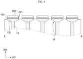
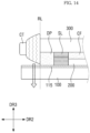
- FIG. 7 is a cross-sectional view taken along line B-B' of FIG. 1 according to one embodiment
- FIG. 8 is a cross-sectional view taken along line B-B' of FIG. 1 according to another embodiment
- FIG. 9 is a cross-sectional view taken along line B-B' of FIG. 2 according to still another embodiment.
- At least one side surface S1 of a display device 1 may include flat portions FP and recessed portions TP.
- a cross section of each of the recessed portions TP taken along line B-B' may have a round shape, and the recessed portions TP may be disposed to be spaced apart from each other in the first direction DR1. That is, the flat portions FP and the recessed portions TP may be alternately disposed in the first direction DR1, ends of connection lines 115 may be exposed by the recessed portions TP, and connection pads 130 may be in contact with the ends of the connection lines 115 of the recessed portions TP.
- a plurality of recessed portions TP may be disposed in the form of being connected to each other in the first direction DR1. That is, the plurality of recessed portions TP may be disposed in the form of being connected to each other without the flat portions FP, and radius curvatures thereof may be different from the radius curvatures of the recessed portions TP shown in FIG. 7 .
- recessed portions TP may be disposed in the form of a bar in the first direction DR1. That is, the recessed portions TP may be disposed in the form of a bar in the first direction DR1, ends of connection lines 115 may be separated and exposed by the recessed portions TP, and connection pads 130 may be connected to the ends of the connection lines 115 to correspond thereto.
- the recessed portions TP may be disposed to correspond to the connection lines 115, but the present invention is not limited thereto.
- One recessed portion TP may be disposed to correspond to a group of a plurality of connection lines 115.
- connection pads 130 may be disposed to correspond to the plurality of recessed portions TP.
- the present invention is not limited thereto, and a plurality of connection pads 130 may be disposed to correspond to one recessed portion TP.
- the connection pads 130 may be disposed to correspond to the plurality of connection lines 115 which are disposed in the one recessed portion TP.
- the contact pads CP1 of the flexible printed circuit boards SFPC1 may be electrically connected to the connection pads 130 through the adhesive films 400.
- connection lines 115 and the connection pads 130 are in contact with each other at the inner side IS of the reference line RL through the recessed portions TP so that it is possible to effectively prevent an open between the connection lines 115 and the connection pads 130.
- FIG. 10 is a cross-sectional view taken along line A-A' of FIG. 2 according to another embodiment.
- a display device of FIG. 10 has a structure that is the same as the structure of FIG. 4 except for a shape of a connection pad. Hereinafter, a duplicate description thereof will be omitted.
- connection pad 130 may include a first portion BP disposed to be flat at the outer side OS of the reference line RL in the third direction DR3, and a second portion PP convexly protruding from the first portion BP toward the inner side IS of the reference line RL. That is, the connection pads 130 may include the second portion PP filling the recessed portion TP based on the first portion BP, and the second portion PP is in contact with a connection line 115 at the inner side IS of the reference line RL to be electrically connected to the connection line 115.
- a surface of the first portion BP of the connection pads 130, which is opposite to one surface on which the second portion PP is disposed, is formed to be flat so that a bonding area with an adhesive film 400 is increased.
- FIG. 11 is a cross-sectional view taken along line A-A' of FIG. 2 according to still another embodiment
- FIG. 12 is a schematic cross-sectional view illustrating a portion of FIG. 10 to describe a recessed portion.
- Display devices of FIGS. 11 and 12 have structures that are the same as the structures of FIGS. 4 and 5 except for shapes of a recessed portion and a connection pad. Hereinafter, a duplicate description thereof will be omitted.
- At least one side surface S1 of a display device 1 may include a flat portion FP and a recessed portions TP.
- the recessed portion TP formed from the flat portion FP of the one side surface S1 of the display device 1 in a direction toward a central portion of the display device 1 (the second direction DR2) may be included.
- the flat portion FP may serve as a buffer to prevent damage of a first substrate 100 in which the recessed portion TP is disposed and a side surface of a second substrate 300 due to an external impact.
- the recessed portion TP may have a form in which portions of the first substrate 100, the connection line 115, a dummy pattern DP, and the second substrate 300 are polished. That is, the recessed portion TP may have a prism shape disposed over the first substrate 100, a connection line 115, a dummy pattern DP, and the second substrate 300 based on a cross section taken along line A-A'. However, the present invention is not limited thereto, and the recessed portion TP may be disposed over some components among the first substrate 100, the connection line 115, the dummy pattern DP, and the second substrate 300.
- the recessed portion TP may be a form in which some portions of the first substrate 100, the connection line 115, and the dummy pattern DP are polished or may be a form in which some portions of the second substrate 300, the dummy pattern DP, and the connection line 115 are polished.
- connection line 115 may have an inclined cross section due to the recessed portion TP.
- the recessed portion TP may include first and second inclined surfaces TPL1 and TPL2 which are inclined from an end of a flat portion FP of each of the first and second substrates 100 and 300 toward a central portion C.
- a depth d of the recessed portion TP may be increased in a direction toward the central portion C which is a position where the first inclined surface TPL1 and the second inclined surface TPL2 meet, and a position of the central portion C may be located at a center of the dummy pattern DP, but the present invention is not limited thereto, and the position of the central portion C may be biased toward either the first substrate 100 or the second substrate 300.
- a cross section of the recessed portion TP may have various shapes such as an equilateral triangle, an isosceles triangle, and a right-angled triangle.
- the recessed portion TP may include first to fourth regions TP1, TP2, TP3, and TP4.
- the shape of the recessed portion TP may include the first region TP1 exposing the bare glass of the second substrate 300, the second region TP2 disposed between the first substrate 100 and the second substrate 300, a third region TP3 exposing the end of the connection line 115, and a fourth region TP4 exposing the bare glass of the first substrate 100.
- the component exposed by the second region TP2 of the recessed portion TP may be varied according to a component disposed at an edge between the first substrate 100 and the second substrate 300.
- the dummy pattern DP since the dummy pattern DP is disposed, the dummy pattern DP is exposed by the second region TP2 of the recessed portion TP, and the recessed portion TP and a sealant SL are disposed to be spaced apart from each other. However, when the dummy pattern DP is omitted, the sealant SL may be exposed by the recessed portion TP.
- the first inclined surface TPL1 may be formed by the first and second regions TP1 and TP2 of the recessed portion TP
- the second inclined surface TPL2 may be formed by the third and fourth regions TP3 and TP4 of the recessed portion TP
- the first inclined surface TPL1 and the second inclined surface TPL2 may be symmetrical, but the present invention is not limited thereto, and the first inclined surface TPL1 and the second inclined surface TPL2 may be asymmetrical.
- the component exposed by the second region TP2 of the recessed portion TP may be varied according to a component disposed at an edge between the first substrate 100 and the second substrate 300.
- the dummy pattern DP since the dummy pattern DP is disposed, the dummy pattern DP of which one side surface is recessed in a prism shape is exposed due to the second region TP2 of the recessed portion TP, and the recessed portion TP and a sealant SL are disposed to be spaced apart from each other.
- the sealant SL of which one side surface is recessed in a prism shape due to the recessed portion TP may be exposed.
- connection pad 130 is disposed to cover the recessed portion TP.
- the connection pad 130 may include a first portion 130a disposed in the flat portion FP of the one side surface S 1 of the display device 1, and a second portion 130b disposed in the recessed portion TP.
- the first portion 130a may be disposed in an outer side OS of the reference line RL, and the second portion 130b may be disposed in an inner side IS of the reference line RL, but the present invention is not limited thereto, and shapes of the first portion 130a and the second portion 130b may be variously modified according to a material constituting the connection pad 130 and a manufacturing process thereof.
- the second portion 130b of the connection pad 130 may be disposed on the first inclined surface TPL1 and the second inclined surface TPL2. That is, the second portion 130b may be disposed along the first inclined surface TPL1 formed by the first and second regions TP1 and TP2 and the second inclined surface TPL2 formed by the third and fourth regions TP3 and TP4 of the recessed portion TP.
- connection pad 130 may be in direct contact with the bare glass of the second substrate 300 exposed by the first region TP1 of the of the recessed portion TP, a side surface of the dummy pattern DP exposed by the second region TP2 of the recessed portion TP between the first substrate 100 and the second substrate 300, the end of the connection line 115 exposed by the third region TP3 of the recessed portion TP, and the bare glass of the first substrate 100 exposed by the fourth region TP4 of recessed portion TP to be disposed along morphology of the recessed portion TP.
- connection pad 130 is electrically connected to be in contact with the end of connection line 115 which is exposed by the third region TP3 of the recessed portion TP at the inner side IS of the reference line RL.
- the connection pad 130 may be made of Al or Ag, but the present invention is limited thereto.
- the adhesive film 400 may be disposed outside the connection pad 130.
- the adhesive film 400 may electrically connect the connection pad 130 to a contact pad CP1 of the flexible printed circuit board SFPC1. Since the connection pad 130 is disposed along the morphology of the recessed portion TP, a void H may be formed between the connection pad 130 and the adhesive film 400 to correspond to the recessed portion.
- the present invention is not limited thereto, and the adhesive film 400 may be disposed along the morphology of the connection pad 130.
- connection pads 130 and the contact pad CP1 may be in direct contact with each other without the adhesive film 400 to be electrically connected.
- the connection pads 130 and the contact pad CP1 may be directly connected by an ultrasonic bonding method or a welding method.
- the recessed portion TP is disposed in at least one side surface S1 of the display device 1 so that the connection line 115 and the connection pad 130 are in contact with each other at the inner side IS of the reference line RL, in a polishing process in which the first substrate 100 and the second substrate 300 are coplanarly disposed, it is possible to effectively prevent the connection line 115 from being damaged to effectively prevent the connection line 115 and the connection pads 130 from being open due to foreign materials that are generated and accumulated on the connection line 115 during the polishing process.
- FIG. 13 is a cross-sectional view taken along line A-A' of FIG. 2 according to still another embodiment.
- a display device of FIG. 13 has a structure that is the same as the structure of FIG. 11 except for a shape of a connection pad. Hereinafter, a duplicate description thereof will be omitted.
- connection pad 130 may include a first portion BP disposed to be flat at the outer side OS of the reference line RL in the third direction DR3, and a second portion PP of a prism shape protruding from the first portion BP toward the inner side IS of the reference line RL. That is, the connection pads 130 may include the second portion PP filling the recessed portion TP based on the first portion BP, and the second portion PP is in contact with a connection line 115 of a first substrate 100 at the inner side IS of the reference line RL to be electrically connected to the connection line 115.
- a surface of the first portion BP of the connection pads 130, which is opposite to one surface on which the second portion PP is disposed, is formed to be flat so that a bonding area with an adhesive film 400 is increased.
- FIGS. 14 to 24 are cross-sectional views illustrating a method of manufacturing a display device of the present invention. Components which are substantially the same as those in FIG. 4 will be denoted by the same reference numerals and a detailed description thereof will be omitted.
- a polishing process may be performed by any one among physical polishing, chemical polishing, chemical mechanical polishing, and electro polishing, and the physical polishing will be described.
- the display device 1 may be formed using the first and second substrates 100 and 300 which are bonded with the liquid crystal layer 200 interposed therebetween.
- the first substrate 100 may have a shape protruding outward from the second substrate 300, and the first substrate 100 is polished using the reference line RL extending from a side surface of the second substrate 300 in the third direction DR3 as a polishing angle.
- the display device 1 is fixed to a polishing table, and a polishing device CT is moved along the reference line RL connecting the outer surface 100a of the first substrate 100 (see FIG. 5 ) to the outer surface 300a of the second substrate 300 (see FIG. 5 ) in the third direction DR3 to polish the first substrate 100.
- the side surfaces of the first substrate 100 and the second substrate 300 may be aligned along the reference line RL, and a bezel BZ formed such that the first substrate 100 protrudes outward from the second substrate 300 may be removed.
- the connection line 150 formed in the first substrate 100 is also polished along the reference line RL.
- the first polishing process may be omitted.
- a second polishing process in which the side surfaces of the first and second substrates 100 and 300 aligned along the reference line RL are polished in the second direction DR2, is shown. That is, portions of the first and second substrates 100 and 300, the connection line 115, and the dummy pattern DP are polished in the second direction DR2 through the polishing device CT to form the recessed portion TP at one side of the display device 1. Owing to the recessed portion TP, bare glass of the second substrate 300 is exposed, a predetermined groove is formed in the dummy pattern DP, and an end of the connection line 115 is exposed inside the reference line RL, and bare glass of the first substrate 100 is exposed.
- the second polishing process may be performed in the second direction DR2 using the polishing device CT and, simultaneously, may be performed by moving the polishing device CT in the first direction DR1.
- the recessed portion TP in the form of a bar extending in the first direction DR1.
- a depth of the recessed portion TP may be determined in response to a pressure in the second direction DR2, and a length of the recessed portion TP may be determined according to progression of the polishing process in the first direction DR1.
- the side surface of the display device 1 may be partially polished.
- Three recessed portions TP have been formed in one side surface of the display device 1, but the present invention is not limited thereto.
- a plurality of recessed portions TP spaced apart from each other may be formed by applying a pressure to a part of one side surface of the display device 1 in the second direction DR2 through the polishing device CT.
- connection pad 130 is formed on a side surface of the display device 1. That is, the connection pad 130 is formed in a shape corresponding to the side surface of the display device 1 in which the recessed portion TP is formed.
- the connection pad 130 may be formed such that a connection pad layer is formed by a plating or sputtering method using Al or Ag and then is patterned.
- connection pad 130 may include a first portion BP disposed to be flat at the outer side OS of the reference line RL in the third direction DR3 and a second portion PP convexly protruding from the first portion BP toward the inner side IS of the reference line RL, and the second portion PP is in contact with the connection line 115 to be electrically connected thereto at the inner side IS of the reference line RL.
- the recessed portion TP is disposed on at least one side surface S1 of the display device 1 so that the connection line 115 and the connection pad 130 may be in contact with each other at the inner side IS of the reference line RL, in a polishing process in which the first substrate 100 and the second substrate 300 are coplanarly arranged, it is possible to effectively prevent the connection line 115 from being damaged to effectively prevent the connection line 115 and the connection pads 130 from being open due to foreign materials that are generated and accumulated on the connection line 115 during the polishing process.
- connection pad layer may be formed through a process of applying and curing a conductive paste such as Al or Ag, and the connection pad layer may be patterned to form the connection pad 130.
- the connection pad 130 may include a first portion BP disposed to be flat at the outer side OS of the reference line RL in the third direction DR3 and a second portion PP convexly protruding from the first portion BP toward the inner side IS of the reference line RL, and a surface of the first portion BP of the connection pads 130, which is opposite to one surface on which the second portion PP is disposed, may be formed to be flat to be stably connected to a flexible printed circuit board SFPC1.
- a flexible printed circuit board SFPC1 to which a driving printed circuit board SPCB 1 is connected is bonded to one side of the display device 1 on which a connection pad 130 is formed.
Landscapes
- Physics & Mathematics (AREA)
- Nonlinear Science (AREA)
- Chemical & Material Sciences (AREA)
- Mathematical Physics (AREA)
- Crystallography & Structural Chemistry (AREA)
- General Physics & Mathematics (AREA)
- Optics & Photonics (AREA)
- Engineering & Computer Science (AREA)
- Microelectronics & Electronic Packaging (AREA)
- Inorganic Chemistry (AREA)
- Devices For Indicating Variable Information By Combining Individual Elements (AREA)
- Liquid Crystal (AREA)
Claims (12)
- Anzeigevorrichtung, umfassend:ein erstes Substrat (100), das eine Verbindungsleitung (115) beinhaltet;ein zweites Substrat (300), das dem ersten Substrat zugewandt ist; undein Verbindungspad (130), das an eine Seitenfläche des ersten Substrats und eine Seitenfläche des zweiten Substrats gekoppelt ist, wobei die eine Seitenfläche des ersten Substrats und die eine Seitenfläche des zweiten Substrats in einer ersten Richtung senkrecht zu oberen Flächen des ersten Substrats und des zweiten Substrats angeordnet sind,wobei das Verbindungspad einen ersten Abschnitt (130a), der mit der einen Seitenfläche des ersten Substrats und der einen Seitenfläche des zweiten Substrats in Kontakt steht, und einen zweiten Abschnitt (130b) beinhaltet, der zwischen dem ersten Substrat und dem zweiten Substrat angeordnet ist, um mit der Verbindungsleitung in Kontakt zu stehen,wobei sich ein Ende der Verbindungsleitung zwischen dem ersten Substrat und dem zweiten Substrat befindet, die in der ersten Richtung angeordnet sind;wobei die Anzeigevorrichtung ferner einen vertieften Abschnitt, TP, umfasst, der über der einen Seitenfläche des ersten Substrats und der einen Seitenfläche des zweiten Substrats angeordnet ist, wobei das Verbindungspad so angeordnet ist, dass es den vertieften Abschnitt abdeckt.
- Anzeigevorrichtung nach Anspruch 1, wobei:jedes von dem ersten Substrat und dem zweiten Substrat Glas beinhaltet; undder vertiefte Abschnitt, TP, eine erste Region, die eine Fläche des Glases des ersten Substrats (100) freilegt, und eine zweite Region beinhaltet, die eine Fläche des Glases des zweiten Substrats (300) freilegt.
- Anzeigevorrichtung nach Anspruch 2, wobei der vertiefte Abschnitt, TP, ferner eine dritte Region beinhaltet, die zwischen der ersten Region und der zweiten Region angeordnet ist und das Ende der Verbindungsleitung (115) freilegt, die sich innerhalb von jedem von dem ersten Substrat und dem zweiten Substrat befindet.
- Anzeigevorrichtung nach Anspruch 3, ferner umfassend ein Blindmuster, DP, das zwischen dem ersten Substrat (100) und dem zweiten Substrat (300) angeordnet ist,
wobei der vertiefte Abschnitt, TP, ferner eine vierte Region beinhaltet, die zwischen der ersten Region und der dritten Region angeordnet ist und das Blindmuster freilegt. - Anzeigevorrichtung nach Anspruch 4, wobei der zweite Abschnitt (130b) des Verbindungspads (130) entlang einer Morphologie der ersten bis vierten Region angeordnet ist.
- Anzeigevorrichtung nach Anspruch 5, wobei der zweite Abschnitt (130b) des Verbindungspads mit der Fläche des Glases von jedem von dem ersten Substrat (100) und dem zweiten Substrat (300) in Kontakt steht.
- Anzeigevorrichtung nach Anspruch 6, wobei der zweite Abschnitt (130b) des Verbindungspads mit jedem von dem Ende der Verbindungsleitung (115) und dem Blindmuster, DP, in Kontakt steht.
- Anzeigevorrichtung nach Anspruch 4, wobei der erste Abschnitt (130a) des Verbindungspads ein flacher Abschnitt ist, der sich in die erste Richtung erstreckt, und der zweite Abschnitt (130b) ein nach innen zwischen dem ersten Substrat (100) und dem zweiten Substrat (300) hervorstehender Vorsprung ist.
- Anzeigevorrichtung nach Anspruch 8, wobei der Vorsprung mit der Fläche des Glases von jedem von dem ersten Substrat (100) und dem zweiten Substrat (300) in Kontakt steht.
- Anzeigevorrichtung nach Anspruch 9, wobei der Vorsprung mit jedem von dem Ende der Verbindungsleitung und dem Blindmuster in Kontakt steht.
- Anzeigevorrichtung nach Anspruch 1, ferner umfassend:ein Dichtungselement, SL, das entlang von Randregionen des ersten Substrats (100) und des zweiten Substrats (300) angeordnet ist, um das erste Substrat an das zweite Substrat zu koppeln; undeine Flüssigkristallschicht (200), die zwischen dem ersten Substrat und dem zweiten Substrat in einer inneren Region des Dichtungselements angeordnet ist,wobei der vertiefte Abschnitt, der über der einen Seitenfläche des ersten Substrats angeordnet ist, eine erste geneigte Fläche, TPL1, beinhaltet, die in Bezug auf jede von einer ersten Seitenfläche und einer oberen Fläche in einer ersten Eckregion, in der die sich außerhalb des Dichtungselements befindende erste Seitenfläche und die dem zweiten Substrat zugewandte obere Fläche zusammentreffen, geneigt ist, undder vertiefte Abschnitt, der über der einen Seitenfläche des zweiten Substrats angeordnet ist, eine zweite geneigte Fläche, TPL2, beinhaltet, die sich außerhalb des Dichtungselements befindet und in Bezug auf eine zweite Seitenfläche und eine untere Fläche in einer zweiten Eckregion, in der die zweite Seitenfläche mit der ersten Seitenfläche und der dem ersten Substrat zugewandten unteren Fläche ausgerichtet ist, geneigt ist.
- Anzeigevorrichtung nach Anspruch 11, ferner umfassend ein Blindmuster, DP, das außerhalb des Dichtungselements, SL, angeordnet ist,wobei das erste Substrat (100) einen ersten Knickpunkt beinhaltet, an dem die erste geneigte Fläche, TPL1, auf die obere Fläche des ersten Substrats trifft,das zweite Substrat (300) einen zweiten Knickpunkt beinhaltet, an dem die zweite geneigte Fläche, TPL2, auf die unter Fläche des zweiten Substrats trifft, unddas Blindmuster in einem Raum zwischen dem Dichtungselement und einer Knickreferenzlinie angeordnet ist, die eine gerade Linie ist, die den ersten Knickpunkt mit dem zweiten Knickpunkt verbindet, wobei eine Außenfläche des Blindmusters eine erste geneigte Region, die eine Neigung aufweist, die sich von der ersten geneigten Fläche erstreckt, und eine zweite geneigte Region beinhalten kann, die eine Neigung aufweist, die sich von der zweiten geneigten Fläche erstreckt,oder wobei:die erste geneigte Fläche eine erste konkave Fläche ist, die eine erste Krümmung aufweist;die zweite geneigte Fläche eine zweite konkave Fläche ist, die eine zweite Krümmung aufweist;die Außenfläche des Blindmusters eine erste konkave Region beinhaltet, die sich von der ersten geneigten Fläche erstreckt und die erste Krümmung aufweist; unddie Außenfläche des Blindmusters eine zweite konkave Region beinhaltet, die sich von der zweiten geneigten Fläche erstreckt und die zweite Krümmung aufweist, wobei optional die erste Krümmung gleich der zweiten Krümmung ist.
Applications Claiming Priority (2)
| Application Number | Priority Date | Filing Date | Title |
|---|---|---|---|
| KR1020180095181A KR102731395B1 (ko) | 2018-08-14 | 2018-08-14 | 표시장치 및 그 제조방법 |
| PCT/KR2019/001571 WO2020036277A1 (ko) | 2018-08-14 | 2019-02-08 | 표시장치 및 그 제조방법 |
Publications (3)
| Publication Number | Publication Date |
|---|---|
| EP3828626A1 EP3828626A1 (de) | 2021-06-02 |
| EP3828626A4 EP3828626A4 (de) | 2022-04-06 |
| EP3828626B1 true EP3828626B1 (de) | 2024-08-07 |
Family
ID=69524791
Family Applications (1)
| Application Number | Title | Priority Date | Filing Date |
|---|---|---|---|
| EP19849494.0A Active EP3828626B1 (de) | 2018-08-14 | 2019-02-08 | Anzeigevorrichtung |
Country Status (7)
| Country | Link |
|---|---|
| US (2) | US11809050B2 (de) |
| EP (1) | EP3828626B1 (de) |
| JP (1) | JP7382393B2 (de) |
| KR (1) | KR102731395B1 (de) |
| CN (1) | CN112567292B (de) |
| TW (1) | TWI828724B (de) |
| WO (1) | WO2020036277A1 (de) |
Families Citing this family (12)
| Publication number | Priority date | Publication date | Assignee | Title |
|---|---|---|---|---|
| KR102766998B1 (ko) * | 2019-02-19 | 2025-02-12 | 삼성디스플레이 주식회사 | 표시 장치 및 그 제조 방법 |
| CN110828480A (zh) * | 2019-11-13 | 2020-02-21 | 京东方科技集团股份有限公司 | 显示面板及其制作方法和显示装置 |
| KR102827103B1 (ko) * | 2020-02-24 | 2025-07-02 | 삼성디스플레이 주식회사 | 표시 장치 및 그것의 제조 방법 |
| KR102795420B1 (ko) * | 2020-02-25 | 2025-04-14 | 삼성디스플레이 주식회사 | 표시 장치 및 표시 장치의 제조 방법 |
| CN113889499A (zh) * | 2020-07-01 | 2022-01-04 | 群创光电股份有限公司 | 电子装置 |
| TWI737520B (zh) * | 2020-08-14 | 2021-08-21 | 友達光電股份有限公司 | 顯示面板 |
| CN113257127B (zh) * | 2020-08-14 | 2023-03-14 | 友达光电股份有限公司 | 显示装置 |
| CN113568224B (zh) * | 2020-08-14 | 2022-10-21 | 友达光电股份有限公司 | 显示装置 |
| US12148741B2 (en) | 2021-08-20 | 2024-11-19 | Apple Inc. | Sidewall connections and button interconnects for molded SiPs |
| US11765838B2 (en) * | 2021-08-20 | 2023-09-19 | Apple Inc. | Right angle sidewall and button interconnects for molded SiPs |
| KR102822075B1 (ko) | 2021-12-31 | 2025-06-18 | 삼성전자주식회사 | 디스플레이 패널 및 그의 제조 방법 |
| CN116068795A (zh) * | 2023-04-06 | 2023-05-05 | 深圳铭创智能装备有限公司 | 液晶显示屏的加工方法、液晶显示屏及大幅面拼接屏 |
Family Cites Families (27)
| Publication number | Priority date | Publication date | Assignee | Title |
|---|---|---|---|---|
| JPH10339879A (ja) * | 1997-06-09 | 1998-12-22 | Toshiba Electron Eng Corp | 液晶表示パネル及びその製造方法 |
| JPH1195237A (ja) * | 1997-09-17 | 1999-04-09 | Canon Inc | 電極基板、該電極基板の製造方法、液晶素子、該液晶素子の製造方法及び電極基板の製造装置 |
| KR100532866B1 (ko) * | 1999-02-26 | 2005-12-01 | 삼성전자주식회사 | 타일드 액정표시장치용 엘씨디 모듈 |
| KR100715247B1 (ko) * | 2004-08-24 | 2007-05-07 | 황영모 | 전자 액정창 및 그 제조 방법 |
| US8395746B2 (en) * | 2006-01-31 | 2013-03-12 | Semiconductor Energy Laboratory Co., Ltd. | Display device |
| JP5569900B2 (ja) | 2009-09-29 | 2014-08-13 | 株式会社aLab | 耐震性能評価方法、耐震性能評価装置及び耐震性能評価システム |
| JPWO2011052485A1 (ja) | 2009-10-26 | 2013-03-21 | 旭硝子株式会社 | ディスプレイ用ガラス基板及びその製造方法 |
| KR20110124488A (ko) * | 2010-05-11 | 2011-11-17 | 엘지전자 주식회사 | 연성 기판과 이를 이용한 디스플레이 장치, 플라즈마 디스플레이 장치, 멀티 디스플레이 장치 및 멀티 플라즈마 디스플레이 장치 |
| KR101431752B1 (ko) * | 2012-12-11 | 2014-08-22 | 엘지디스플레이 주식회사 | 디스플레이 장치 및 디스플레이 패널의 측면 실링 장치 |
| US8994042B2 (en) * | 2013-05-20 | 2015-03-31 | Lg Electronics Inc. | Display panel and display device |
| KR102050449B1 (ko) | 2013-07-23 | 2019-11-29 | 엘지디스플레이 주식회사 | 보더리스 타입의 액정 표시 장치 |
| KR102230752B1 (ko) * | 2013-12-20 | 2021-03-19 | 엘지디스플레이 주식회사 | 표시장치 및 표시장치의 제조방법 |
| JP2015196620A (ja) | 2014-04-01 | 2015-11-09 | 凸版印刷株式会社 | カバーガラス及び表示装置 |
| TWI671721B (zh) * | 2014-09-15 | 2019-09-11 | 比利時商巴而可公司 | 顯示磚、用於顯示磚的框架及其製作方法 |
| JP6282581B2 (ja) | 2014-12-22 | 2018-02-21 | エルジー ディスプレイ カンパニー リミテッド | 電子部品の実装方法 |
| US10310341B2 (en) | 2015-06-29 | 2019-06-04 | Lg Display Co., Ltd. | Display device and method of manufacturing the same |
| KR102584326B1 (ko) * | 2015-06-29 | 2023-10-04 | 엘지디스플레이 주식회사 | 디스플레이 장치 및 그 제조 방법 |
| KR102387880B1 (ko) | 2015-07-03 | 2022-04-18 | 엘지디스플레이 주식회사 | 디스플레이 장치 |
| KR102378891B1 (ko) | 2015-09-18 | 2022-03-24 | 엘지디스플레이 주식회사 | 디스플레이 패널 및 이를 포함하는 디스플레이 장치 |
| KR102429136B1 (ko) * | 2015-10-30 | 2022-08-03 | 엘지디스플레이 주식회사 | 디스플레이 장치 |
| KR20170080937A (ko) * | 2015-12-31 | 2017-07-11 | 엘지디스플레이 주식회사 | 측면 접합 구조를 갖는 디스플레이 장치 및 그 제조방법 |
| KR102568933B1 (ko) * | 2016-05-31 | 2023-08-23 | 엘지디스플레이 주식회사 | 디스플레이 장치 |
| KR102652604B1 (ko) | 2016-06-08 | 2024-04-02 | 삼성디스플레이 주식회사 | 표시 장치 및 이의 제조 방법 |
| KR102645333B1 (ko) | 2016-08-23 | 2024-03-12 | 삼성디스플레이 주식회사 | 표시장치 |
| KR102671559B1 (ko) | 2016-09-07 | 2024-06-04 | 삼성디스플레이 주식회사 | 표시장치 |
| TWI646370B (zh) | 2017-12-26 | 2019-01-01 | 友達光電股份有限公司 | 顯示裝置及其製作方法 |
| CN108153070A (zh) * | 2017-12-29 | 2018-06-12 | 惠州市华星光电技术有限公司 | 一种液晶面板及其制作方法、显示装置 |
-
2018
- 2018-08-14 KR KR1020180095181A patent/KR102731395B1/ko active Active
-
2019
- 2019-02-08 CN CN201980054037.3A patent/CN112567292B/zh active Active
- 2019-02-08 JP JP2021507496A patent/JP7382393B2/ja active Active
- 2019-02-08 WO PCT/KR2019/001571 patent/WO2020036277A1/ko not_active Ceased
- 2019-02-08 EP EP19849494.0A patent/EP3828626B1/de active Active
- 2019-02-08 US US17/267,966 patent/US11809050B2/en active Active
- 2019-07-24 TW TW108126218A patent/TWI828724B/zh active
-
2023
- 2023-10-20 US US18/491,336 patent/US12313944B2/en active Active
Also Published As
| Publication number | Publication date |
|---|---|
| JP2021534449A (ja) | 2021-12-09 |
| US20240045284A1 (en) | 2024-02-08 |
| EP3828626A4 (de) | 2022-04-06 |
| US11809050B2 (en) | 2023-11-07 |
| TWI828724B (zh) | 2024-01-11 |
| WO2020036277A1 (ko) | 2020-02-20 |
| US12313944B2 (en) | 2025-05-27 |
| CN112567292B (zh) | 2024-11-08 |
| TW202009569A (zh) | 2020-03-01 |
| JP7382393B2 (ja) | 2023-11-16 |
| US20210200006A1 (en) | 2021-07-01 |
| KR20200019813A (ko) | 2020-02-25 |
| EP3828626A1 (de) | 2021-06-02 |
| CN112567292A (zh) | 2021-03-26 |
| KR102731395B1 (ko) | 2024-11-18 |
Similar Documents
| Publication | Publication Date | Title |
|---|---|---|
| EP3828626B1 (de) | Anzeigevorrichtung | |
| KR102795420B1 (ko) | 표시 장치 및 표시 장치의 제조 방법 | |
| CN111724707B (zh) | 显示装置 | |
| KR102600528B1 (ko) | 표시 장치 | |
| US11181762B2 (en) | Display device | |
| CN112748612B (zh) | 显示设备 | |
| CN111697035B (zh) | 显示设备 | |
| KR20190142797A (ko) | 표시 장치 |
Legal Events
| Date | Code | Title | Description |
|---|---|---|---|
| STAA | Information on the status of an ep patent application or granted ep patent |
Free format text: STATUS: THE INTERNATIONAL PUBLICATION HAS BEEN MADE |
|
| PUAI | Public reference made under article 153(3) epc to a published international application that has entered the european phase |
Free format text: ORIGINAL CODE: 0009012 |
|
| STAA | Information on the status of an ep patent application or granted ep patent |
Free format text: STATUS: REQUEST FOR EXAMINATION WAS MADE |
|
| 17P | Request for examination filed |
Effective date: 20210225 |
|
| AK | Designated contracting states |
Kind code of ref document: A1 Designated state(s): AL AT BE BG CH CY CZ DE DK EE ES FI FR GB GR HR HU IE IS IT LI LT LU LV MC MK MT NL NO PL PT RO RS SE SI SK SM TR |
|
| DAV | Request for validation of the european patent (deleted) | ||
| DAX | Request for extension of the european patent (deleted) | ||
| A4 | Supplementary search report drawn up and despatched |
Effective date: 20220304 |
|
| RIC1 | Information provided on ipc code assigned before grant |
Ipc: G02F 1/1333 20060101ALI20220228BHEP Ipc: H05K 1/14 20060101ALI20220228BHEP Ipc: G02F 1/1345 20060101AFI20220228BHEP |
|
| P01 | Opt-out of the competence of the unified patent court (upc) registered |
Effective date: 20230516 |
|
| GRAP | Despatch of communication of intention to grant a patent |
Free format text: ORIGINAL CODE: EPIDOSNIGR1 |
|
| STAA | Information on the status of an ep patent application or granted ep patent |
Free format text: STATUS: GRANT OF PATENT IS INTENDED |
|
| RIC1 | Information provided on ipc code assigned before grant |
Ipc: G02F 1/1333 20060101ALN20240205BHEP Ipc: G02F 1/13 20060101ALN20240205BHEP Ipc: H10K 59/131 20230101ALI20240205BHEP Ipc: H05K 1/14 20060101ALI20240205BHEP Ipc: H05K 1/11 20060101ALI20240205BHEP Ipc: G02F 1/1345 20060101AFI20240205BHEP |
|
| INTG | Intention to grant announced |
Effective date: 20240311 |
|
| GRAS | Grant fee paid |
Free format text: ORIGINAL CODE: EPIDOSNIGR3 |
|
| GRAA | (expected) grant |
Free format text: ORIGINAL CODE: 0009210 |
|
| STAA | Information on the status of an ep patent application or granted ep patent |
Free format text: STATUS: THE PATENT HAS BEEN GRANTED |
|
| AK | Designated contracting states |
Kind code of ref document: B1 Designated state(s): AL AT BE BG CH CY CZ DE DK EE ES FI FR GB GR HR HU IE IS IT LI LT LU LV MC MK MT NL NO PL PT RO RS SE SI SK SM TR |
|
| REG | Reference to a national code |
Ref country code: GB Ref legal event code: FG4D |
|
| REG | Reference to a national code |
Ref country code: CH Ref legal event code: EP |
|
| REG | Reference to a national code |
Ref country code: IE Ref legal event code: FG4D |
|
| REG | Reference to a national code |
Ref country code: DE Ref legal event code: R096 Ref document number: 602019056732 Country of ref document: DE |
|
| REG | Reference to a national code |
Ref country code: LT Ref legal event code: MG9D |
|
| REG | Reference to a national code |
Ref country code: NL Ref legal event code: MP Effective date: 20240807 |
|
| PG25 | Lapsed in a contracting state [announced via postgrant information from national office to epo] |
Ref country code: NO Free format text: LAPSE BECAUSE OF FAILURE TO SUBMIT A TRANSLATION OF THE DESCRIPTION OR TO PAY THE FEE WITHIN THE PRESCRIBED TIME-LIMIT Effective date: 20241107 |
|
| REG | Reference to a national code |
Ref country code: AT Ref legal event code: MK05 Ref document number: 1711602 Country of ref document: AT Kind code of ref document: T Effective date: 20240807 |
|
| PG25 | Lapsed in a contracting state [announced via postgrant information from national office to epo] |
Ref country code: FI Free format text: LAPSE BECAUSE OF FAILURE TO SUBMIT A TRANSLATION OF THE DESCRIPTION OR TO PAY THE FEE WITHIN THE PRESCRIBED TIME-LIMIT Effective date: 20240807 Ref country code: NL Free format text: LAPSE BECAUSE OF FAILURE TO SUBMIT A TRANSLATION OF THE DESCRIPTION OR TO PAY THE FEE WITHIN THE PRESCRIBED TIME-LIMIT Effective date: 20240807 Ref country code: GR Free format text: LAPSE BECAUSE OF FAILURE TO SUBMIT A TRANSLATION OF THE DESCRIPTION OR TO PAY THE FEE WITHIN THE PRESCRIBED TIME-LIMIT Effective date: 20241108 Ref country code: PL Free format text: LAPSE BECAUSE OF FAILURE TO SUBMIT A TRANSLATION OF THE DESCRIPTION OR TO PAY THE FEE WITHIN THE PRESCRIBED TIME-LIMIT Effective date: 20240807 Ref country code: PT Free format text: LAPSE BECAUSE OF FAILURE TO SUBMIT A TRANSLATION OF THE DESCRIPTION OR TO PAY THE FEE WITHIN THE PRESCRIBED TIME-LIMIT Effective date: 20241209 |
|
| PG25 | Lapsed in a contracting state [announced via postgrant information from national office to epo] |
Ref country code: BG Free format text: LAPSE BECAUSE OF FAILURE TO SUBMIT A TRANSLATION OF THE DESCRIPTION OR TO PAY THE FEE WITHIN THE PRESCRIBED TIME-LIMIT Effective date: 20240807 |
|
| PG25 | Lapsed in a contracting state [announced via postgrant information from national office to epo] |
Ref country code: LV Free format text: LAPSE BECAUSE OF FAILURE TO SUBMIT A TRANSLATION OF THE DESCRIPTION OR TO PAY THE FEE WITHIN THE PRESCRIBED TIME-LIMIT Effective date: 20240807 |
|
| PG25 | Lapsed in a contracting state [announced via postgrant information from national office to epo] |
Ref country code: IS Free format text: LAPSE BECAUSE OF FAILURE TO SUBMIT A TRANSLATION OF THE DESCRIPTION OR TO PAY THE FEE WITHIN THE PRESCRIBED TIME-LIMIT Effective date: 20241207 Ref country code: AT Free format text: LAPSE BECAUSE OF FAILURE TO SUBMIT A TRANSLATION OF THE DESCRIPTION OR TO PAY THE FEE WITHIN THE PRESCRIBED TIME-LIMIT Effective date: 20240807 |
|
| PG25 | Lapsed in a contracting state [announced via postgrant information from national office to epo] |
Ref country code: HR Free format text: LAPSE BECAUSE OF FAILURE TO SUBMIT A TRANSLATION OF THE DESCRIPTION OR TO PAY THE FEE WITHIN THE PRESCRIBED TIME-LIMIT Effective date: 20240807 |
|
| PG25 | Lapsed in a contracting state [announced via postgrant information from national office to epo] |
Ref country code: ES Free format text: LAPSE BECAUSE OF FAILURE TO SUBMIT A TRANSLATION OF THE DESCRIPTION OR TO PAY THE FEE WITHIN THE PRESCRIBED TIME-LIMIT Effective date: 20240807 Ref country code: RS Free format text: LAPSE BECAUSE OF FAILURE TO SUBMIT A TRANSLATION OF THE DESCRIPTION OR TO PAY THE FEE WITHIN THE PRESCRIBED TIME-LIMIT Effective date: 20241107 |
|
| PG25 | Lapsed in a contracting state [announced via postgrant information from national office to epo] |
Ref country code: RS Free format text: LAPSE BECAUSE OF FAILURE TO SUBMIT A TRANSLATION OF THE DESCRIPTION OR TO PAY THE FEE WITHIN THE PRESCRIBED TIME-LIMIT Effective date: 20241107 Ref country code: PT Free format text: LAPSE BECAUSE OF FAILURE TO SUBMIT A TRANSLATION OF THE DESCRIPTION OR TO PAY THE FEE WITHIN THE PRESCRIBED TIME-LIMIT Effective date: 20241209 Ref country code: PL Free format text: LAPSE BECAUSE OF FAILURE TO SUBMIT A TRANSLATION OF THE DESCRIPTION OR TO PAY THE FEE WITHIN THE PRESCRIBED TIME-LIMIT Effective date: 20240807 Ref country code: NO Free format text: LAPSE BECAUSE OF FAILURE TO SUBMIT A TRANSLATION OF THE DESCRIPTION OR TO PAY THE FEE WITHIN THE PRESCRIBED TIME-LIMIT Effective date: 20241107 Ref country code: NL Free format text: LAPSE BECAUSE OF FAILURE TO SUBMIT A TRANSLATION OF THE DESCRIPTION OR TO PAY THE FEE WITHIN THE PRESCRIBED TIME-LIMIT Effective date: 20240807 Ref country code: LV Free format text: LAPSE BECAUSE OF FAILURE TO SUBMIT A TRANSLATION OF THE DESCRIPTION OR TO PAY THE FEE WITHIN THE PRESCRIBED TIME-LIMIT Effective date: 20240807 Ref country code: IS Free format text: LAPSE BECAUSE OF FAILURE TO SUBMIT A TRANSLATION OF THE DESCRIPTION OR TO PAY THE FEE WITHIN THE PRESCRIBED TIME-LIMIT Effective date: 20241207 Ref country code: HR Free format text: LAPSE BECAUSE OF FAILURE TO SUBMIT A TRANSLATION OF THE DESCRIPTION OR TO PAY THE FEE WITHIN THE PRESCRIBED TIME-LIMIT Effective date: 20240807 Ref country code: GR Free format text: LAPSE BECAUSE OF FAILURE TO SUBMIT A TRANSLATION OF THE DESCRIPTION OR TO PAY THE FEE WITHIN THE PRESCRIBED TIME-LIMIT Effective date: 20241108 Ref country code: FI Free format text: LAPSE BECAUSE OF FAILURE TO SUBMIT A TRANSLATION OF THE DESCRIPTION OR TO PAY THE FEE WITHIN THE PRESCRIBED TIME-LIMIT Effective date: 20240807 Ref country code: ES Free format text: LAPSE BECAUSE OF FAILURE TO SUBMIT A TRANSLATION OF THE DESCRIPTION OR TO PAY THE FEE WITHIN THE PRESCRIBED TIME-LIMIT Effective date: 20240807 Ref country code: BG Free format text: LAPSE BECAUSE OF FAILURE TO SUBMIT A TRANSLATION OF THE DESCRIPTION OR TO PAY THE FEE WITHIN THE PRESCRIBED TIME-LIMIT Effective date: 20240807 Ref country code: AT Free format text: LAPSE BECAUSE OF FAILURE TO SUBMIT A TRANSLATION OF THE DESCRIPTION OR TO PAY THE FEE WITHIN THE PRESCRIBED TIME-LIMIT Effective date: 20240807 |
|
| PG25 | Lapsed in a contracting state [announced via postgrant information from national office to epo] |
Ref country code: RO Free format text: LAPSE BECAUSE OF FAILURE TO SUBMIT A TRANSLATION OF THE DESCRIPTION OR TO PAY THE FEE WITHIN THE PRESCRIBED TIME-LIMIT Effective date: 20240807 Ref country code: DK Free format text: LAPSE BECAUSE OF FAILURE TO SUBMIT A TRANSLATION OF THE DESCRIPTION OR TO PAY THE FEE WITHIN THE PRESCRIBED TIME-LIMIT Effective date: 20240807 Ref country code: SM Free format text: LAPSE BECAUSE OF FAILURE TO SUBMIT A TRANSLATION OF THE DESCRIPTION OR TO PAY THE FEE WITHIN THE PRESCRIBED TIME-LIMIT Effective date: 20240807 |
|
| PG25 | Lapsed in a contracting state [announced via postgrant information from national office to epo] |
Ref country code: EE Free format text: LAPSE BECAUSE OF FAILURE TO SUBMIT A TRANSLATION OF THE DESCRIPTION OR TO PAY THE FEE WITHIN THE PRESCRIBED TIME-LIMIT Effective date: 20240807 |
|
| PG25 | Lapsed in a contracting state [announced via postgrant information from national office to epo] |
Ref country code: CZ Free format text: LAPSE BECAUSE OF FAILURE TO SUBMIT A TRANSLATION OF THE DESCRIPTION OR TO PAY THE FEE WITHIN THE PRESCRIBED TIME-LIMIT Effective date: 20240807 |
|
| PG25 | Lapsed in a contracting state [announced via postgrant information from national office to epo] |
Ref country code: SK Free format text: LAPSE BECAUSE OF FAILURE TO SUBMIT A TRANSLATION OF THE DESCRIPTION OR TO PAY THE FEE WITHIN THE PRESCRIBED TIME-LIMIT Effective date: 20240807 |
|
| REG | Reference to a national code |
Ref country code: DE Ref legal event code: R097 Ref document number: 602019056732 Country of ref document: DE |
|
| PLBE | No opposition filed within time limit |
Free format text: ORIGINAL CODE: 0009261 |
|
| STAA | Information on the status of an ep patent application or granted ep patent |
Free format text: STATUS: NO OPPOSITION FILED WITHIN TIME LIMIT |
|
| 26N | No opposition filed |
Effective date: 20250508 |
|
| PG25 | Lapsed in a contracting state [announced via postgrant information from national office to epo] |
Ref country code: SE Free format text: LAPSE BECAUSE OF FAILURE TO SUBMIT A TRANSLATION OF THE DESCRIPTION OR TO PAY THE FEE WITHIN THE PRESCRIBED TIME-LIMIT Effective date: 20240807 |
|
| PG25 | Lapsed in a contracting state [announced via postgrant information from national office to epo] |
Ref country code: MC Free format text: LAPSE BECAUSE OF FAILURE TO SUBMIT A TRANSLATION OF THE DESCRIPTION OR TO PAY THE FEE WITHIN THE PRESCRIBED TIME-LIMIT Effective date: 20240807 |
|
| REG | Reference to a national code |
Ref country code: CH Ref legal event code: PL |
|
| PG25 | Lapsed in a contracting state [announced via postgrant information from national office to epo] |
Ref country code: LU Free format text: LAPSE BECAUSE OF NON-PAYMENT OF DUE FEES Effective date: 20250208 |
|
| PG25 | Lapsed in a contracting state [announced via postgrant information from national office to epo] |
Ref country code: CH Free format text: LAPSE BECAUSE OF NON-PAYMENT OF DUE FEES Effective date: 20250228 |
|
| REG | Reference to a national code |
Ref country code: BE Ref legal event code: MM Effective date: 20250228 |
|
| PG25 | Lapsed in a contracting state [announced via postgrant information from national office to epo] |
Ref country code: BE Free format text: LAPSE BECAUSE OF NON-PAYMENT OF DUE FEES Effective date: 20250228 |
|
| PG25 | Lapsed in a contracting state [announced via postgrant information from national office to epo] |
Ref country code: IE Free format text: LAPSE BECAUSE OF NON-PAYMENT OF DUE FEES Effective date: 20250208 |
|
| PG25 | Lapsed in a contracting state [announced via postgrant information from national office to epo] |
Ref country code: IT Free format text: LAPSE BECAUSE OF FAILURE TO SUBMIT A TRANSLATION OF THE DESCRIPTION OR TO PAY THE FEE WITHIN THE PRESCRIBED TIME-LIMIT Effective date: 20240807 |
|
| PGFP | Annual fee paid to national office [announced via postgrant information from national office to epo] |
Ref country code: GB Payment date: 20260122 Year of fee payment: 8 |
|
| PGFP | Annual fee paid to national office [announced via postgrant information from national office to epo] |
Ref country code: DE Payment date: 20260120 Year of fee payment: 8 |
|
| PGFP | Annual fee paid to national office [announced via postgrant information from national office to epo] |
Ref country code: FR Payment date: 20260121 Year of fee payment: 8 |