EP3835774B1 - Gassensor - Google Patents
Gassensor Download PDFInfo
- Publication number
- EP3835774B1 EP3835774B1 EP19847665.7A EP19847665A EP3835774B1 EP 3835774 B1 EP3835774 B1 EP 3835774B1 EP 19847665 A EP19847665 A EP 19847665A EP 3835774 B1 EP3835774 B1 EP 3835774B1
- Authority
- EP
- European Patent Office
- Prior art keywords
- thermistor
- time
- period
- detection element
- reference element
- Prior art date
- Legal status (The legal status is an assumption and is not a legal conclusion. Google has not performed a legal analysis and makes no representation as to the accuracy of the status listed.)
- Active
Links
Images




Classifications
-
- G—PHYSICS
- G01—MEASURING; TESTING
- G01N—INVESTIGATING OR ANALYSING MATERIALS BY DETERMINING THEIR CHEMICAL OR PHYSICAL PROPERTIES
- G01N27/00—Investigating or analysing materials by the use of electric, electrochemical, or magnetic means
- G01N27/02—Investigating or analysing materials by the use of electric, electrochemical, or magnetic means by investigating impedance
- G01N27/04—Investigating or analysing materials by the use of electric, electrochemical, or magnetic means by investigating impedance by investigating resistance
- G01N27/14—Investigating or analysing materials by the use of electric, electrochemical, or magnetic means by investigating impedance by investigating resistance of an electrically-heated body in dependence upon change of temperature
- G01N27/18—Investigating or analysing materials by the use of electric, electrochemical, or magnetic means by investigating impedance by investigating resistance of an electrically-heated body in dependence upon change of temperature caused by changes in the thermal conductivity of a surrounding material to be tested
-
- G—PHYSICS
- G01—MEASURING; TESTING
- G01N—INVESTIGATING OR ANALYSING MATERIALS BY DETERMINING THEIR CHEMICAL OR PHYSICAL PROPERTIES
- G01N33/00—Investigating or analysing materials by specific methods not covered by groups G01N1/00 - G01N31/00
- G01N33/0004—Gaseous mixtures, e.g. polluted air
- G01N33/0009—General constructional details of gas analysers, e.g. portable test equipment
- G01N33/0027—General constructional details of gas analysers, e.g. portable test equipment concerning the detector
- G01N33/0036—General constructional details of gas analysers, e.g. portable test equipment concerning the detector specially adapted to detect a particular component
- G01N33/004—CO or CO2
Definitions
- the present invention relates to a gas sensor for detecting gas contained in the atmosphere and, more particularly, to a gas sensor configured to connect a detection element and a reference element in series.
- Gas sensors detect the concentration of a measurement target gas contained in the atmosphere.
- such gas sensor may be configured to connect a detection element and a reference element in series and acquire an output signal from the connection point therebetween.
- a gas sensor described in Patent Document 1 is configured to connect the detection element and reference element in series and heat them to their respective predetermined temperatures at detection timing.
- the gas sensor described in Patent Document 1 heats the reference element to a high temperature at non-detection timing to reduce the difference in thermal history between the detection element and the reference element.
- the gas sensor described in Patent Document 1 selectively heats only the reference element at non-detection timing, generating a difference in the number of times of heating between the detection element and the reference element. This makes it difficult to set the heating temperature and heating time of the reference element at non-detection timing and, thus, it is not easy to sufficiently reduce the difference in thermal history between the detection element and the reference element.
- a gas sensor according to the present invention is defined in claim 1.
- the reference element has a higher temperature load than the detection element in the first period of time, and the detection element has a higher temperature load than the reference element in the second period of time, so that repeating the first and second periods of time can easily reduce the difference in thermal history between the detection element and the reference element.
- control circuit may calculate the concentration of the gas to be detected based on a potential appearing at a connection point between the detection element and the reference element in one of the first and second periods of time. Thus, it is possible to calculate the concentration of the gas to be detected in one of the first and second periods of time.
- control circuit is configured to heat the first and second heaters such that the detection element and the reference element have a first temperature and a second temperature, respectively, in the first period of time and that the reference element and the detection element have the first temperature and the second temperature, respectively, in the second period of time. This allows the thermal histories of the detection element and reference element to substantially coincide with each other.
- the lengths of the first and second periods of time may be equal to each other. This allows the thermal histories of the detection element and reference element to coincide with each other more accurately.
- the gas to be detected is CO 2 gas
- the heating temperature of the detection element in the first period of time is in the range of 100°C to 200°
- the heating temperature of the reference element in the first period of time is in the range of 250°C to 350°C. This allows the concentration of CO 2 gas to be detected with high sensitivity.
- the detection element and reference element may each have a MEMS structure, and the length of the first period of time may be in the range of 50 ms to 400 ms. This can minimize power consumption.
- the ratio of the resistance value of the detection element and the resistance value of the reference element in the first period of time may be in the range of 0.5 to 2.0. This allows the concentration of CO 2 gas to be detected with high sensitivity.
- the detection element and reference element may be formed on mutually different chips. This makes the heat of the heater provided on one chip less likely to be conducted to the other chip to prevent the detection element and reference element from being suffered from thermal interference from the heaters therefor, thereby suppressing a reduction in sensitivity. Further, the difference in thermal history can be further reduced.
- the thermal histories of the detection element and reference element can be easily reduced. This can suppress the temporal change of the gas sensor.
- FIG. 1 is a circuit diagram illustrating the configuration of a gas sensor 10 according to a preferred embodiment of the present invention.
- the gas sensor 10 As illustrated in FIG. 1 , the gas sensor 10 according to the present embodiment includes a sensor part S and a control circuit 20.
- the gas sensor 10 according to the present invention detects the concentration of CO 2 gas in the atmosphere.
- the sensor part S is a heat conduction type gas sensor for detecting the concentration of CO 2 gas to be detected and has a first sensor part S1 and a second sensor part S2.
- the first sensor part S1 includes a first thermistor Rd1 serving as a detection element and a first heater resistor MH1 that heats the first thermistor Rd1.
- the second sensor part S2 includes a second thermistor Rd2 serving as a reference element and a second heater resistor MH2 that heats the second thermistor Rd2.
- the first and second thermistors Rd1 and Rd2 are connected in series between a wiring supplied with a power supply potential Vcc and a wiring supplied with a ground potential GND.
- the first and second thermistors Rd1 and Rd2 are each made of a material having a negative resistance temperature coefficient, such as a composite metal oxide, amorphous silicon, polysilicon, or germanium.
- the first thermistor Rd1 is heated by the first heater resistor MH1.
- the heating temperature of the first thermistor Rd1 by the first heater resistor MH1 is, e.g., 150°C at detection timing.
- CO 2 gas is present in the measurement atmosphere in a state where the first thermistor Rd1 is heated to 150°C, heat dissipation characteristics of the first thermistor Rd1 changes according to the CO 2 gas concentration. This change appears as a change in the resistance value of the first thermistor Rd1.
- the second thermistor Rd2 is heated by the second heater resistor MH2.
- the heating temperature of the second thermistor Rd2 by the second heater resistor MH2 is, e.g., 300°C at detection timing. Even when CO 2 gas is present in the measurement atmosphere in a state where the second thermistor Rd2 is heated to 300°C, the resistance value of the second thermistor Rd2 hardly changes.
- the ratio of the resistance value of the first thermistor Rd1 and that of the second thermistor Rd2 at a room temperature (25°C) is about 10.
- the resistance values of the first and second thermistors Rd1 and Rd2 at a room temperature are 280 kS2 and 2800 kQ, respectively.
- the heating temperature (e.g., 300°C) of the second thermistor Rd2 at detection timing is higher than the heating temperature (e.g., 150°C) of the first thermistor Rd1 at detection timing, so that, at detection timing, the ratio of the resistance value of the first thermistor Rd1 and the resistance value of the second thermistor Rd2 is in the range of 0.5 to 2.0, preferably, substantially 1.
- the resistance value of the first thermistor Rd1 heated to 150°C is 10 k ⁇
- the resistance value of the second thermistor Rd2 heated to 300°C is also 10 kS2.
- the first and second thermistors Rd1 and Rd2 are connected in series as described above, and a detection signal Vout1 is output from the connection point therebetween.
- the output detection signal Vout1 is input to the control circuit 20.
- the amount of change in the detection signal Vout1 based on the CO 2 gas concentration becomes larger as the resistance values of the first and second thermistors Rd1 and Rd2 at detection timing are closer, and detection sensitivity is improved.
- the ratio of the resistance values of the first and second thermistors Rd1 and Rd2 at detection timing is preferably in the range of 0.5 to 2.0, and particularly preferably, substantially 1.
- the control circuit 20 has differential amplifiers 21 to 23, an AD converter (ADC) 24, a DA converter (DAC) 25, a signal processing part 26, and resistors R1 to R3.
- the differential amplifier 21 compares the detection signal Vout1 and a reference voltage Vref and amplifiers the detected difference.
- the gain of the differential amplifier 21 is adjusted to any value by the resistors R1 to R3.
- An amplified signal Vamp output from the differential amplifier 21 is input to the AD converter 24.
- the AD converter 24 converts the amplified signal Vamp into a digital signal and supplies the obtained value to the signal processing part 26.
- the DA converter converts a reference signal supplied from the signal processing part 26 to an analog signal to generate the reference voltage Vref and generates control voltages Vmh1 and Vmh2 to be supplied respectively to the first and second heater resistors MH1 and MH2.
- the control voltage Vmh1 is applied to the first heater resistor MH1 through a differential amplifier 22 which is a voltage follower.
- the control voltage Vmh2 is applied to the second heater resistor MH2 through a differential amplifier 23 which is a voltage follower.
- FIG. 2 is a top view for explaining the configuration of the sensor part S.
- FIG. 3 is a cross-sectional view taken along line A-A in FIG. 2 .
- the drawings are schematic, and for explanatory convenience, the relation between thickness and plane dimension, ratio between the thicknesses of devices, and the like may be different from those in the actual structure within a range in which the effect of the present embodiment can be obtained.
- the sensor part S is a heat conduction type gas sensor that detects the concentration of a gas based on a change in heat dissipation characteristics according to the CO 2 gas concentration and has, as illustrated in FIGs. 2 and 3 , two sensor parts S1 and S2 and a ceramic package 51 housing the sensor parts S1 and S2.
- the ceramic package 51 is a box-shaped case having an opened upper part, and a lid 52 is provided at the upper part.
- the lid 52 has a plurality of vent holes 53, through which CO 2 gas in the atmosphere can flow into the ceramic package 51. In FIG. 2 , the lid 52 is omitted for ease of viewing.
- the first sensor part S1 includes insulating films 32 and 33 formed respectively on the lower and upper surfaces of a substrate 31, a first heater resistor MH1 provided on the insulating film 33, a heater protective film 34 covering the first heater resistor MH1, a first thermistor Rd1 and a thermistor electrode 35 which are provided on the heater protective film 34, a thermistor protective film 36 covering the first thermistor Rd1 and thermistor electrode 35.
- the material of the substrate 31 there is no particular restriction on the material of the substrate 31 as long as it has an adequate mechanical strength and is suitable for fine processing such as etching, and, examples thereof include a silicon single crystal substrate, a sapphire single crystal substrate, a ceramic substrate, a quartz substrate, a glass substrate, and the like.
- a cavity 31a is provided at a position overlapping the first heater resistor MH1 in a plan view so as to suppress conduction of heat due to the first heater resistor MH1 to the substrate 31.
- a part where the substrate 31 is removed by the cavity 31a is called a membrane. The presence of the membrane reduces heat capacity by the thinning of the substrate 31, allowing heating to be achieved with less power consumption.
- the insulating films 32 and 33 are each made of an insulating material such as silicon oxide or silicon nitride.
- silicon oxide is used as the insulating films 32 and 33
- a film deposition method such as a thermal oxidation method or a CVD (Chemical Vapor Deposition) method may be used.
- the thickness of the insulating films 32 and 33 is used also as an etching stop layer when the cavity 31a is formed in the substrate 31, so that the thickness thereof is preferably set to a value suitable for fulfilling the function as the etching stop layer.
- the first heater resistor MH1 is made of a conductive substance whose resistivity changes depending on temperature and is preferably made of a metal material having a comparatively high melting point, such as molybdenum (Mo), platinum (Pt), gold (Au), tungsten (W), tantalum (Ta), palladium (Pd), iridium (Ir), or an alloy containing two or more of them.
- a conductive material that can be subjected to high accuracy dry etching such as ion milling is preferable, and more preferably, it contains platinum (Pt) having high corrosion resistance as a main component.
- an adhesion layer such as a titanium (Ti) layer is preferably formed as a base of Pt so as to improve adhesion with respect to the insulating film 33.
- the heater protective film 34 is formed above the first heater resistor MH1.
- the heater protective film 34 is preferably made of the same material as the insulating film 33.
- the first heater resistor MH1 generates violent thermal changes (repetition of temperature rises between room temperature to 150°C or 300°C, for example, and then a drop to room temperature again), so that strong thermal stress is applied to the insulating film 33 and heater protective film 34.
- the insulating film 33 and heater protective film 34 may suffer damage such as interlayer peeling or crack.
- the insulating film 33 and the heater protective film 34 are made of the same material, material characteristics thereof are the same, and adhesion strength therebetween is high, so that the damage such as interlayer peeling or crack is less likely to occur as compared to when the insulating film 33 and the heater protective film 34 are made of mutually different materials.
- film deposition may be performed by a thermal oxidation method or a CVD method.
- the film thickness of the heater protective film 34 is not particularly restricted as long as insulation between the first thermistor Rd1 and the thermistor electrode 35 can be ensured and may be, e.g., 0.1 ⁇ m to 3.0 ⁇ m.
- the first thermistor Rd1 is made of a material having a negative resistance-temperature coefficient, such as a composite metal oxide, amorphous silicon, polysilicon, or germanium and can be formed by using a thin-film process such as a sputtering method or a CVD method.
- the film thickness of the first thermistor Rd1 may be adjusted according to a target resistance value.
- the reason that the thermistor is used as a temperature-sensitive resistive element is that the thermistor is larger in resistance temperature coefficient than a platinum temperature detector and can thus obtain high detection sensitivity. Further, heat generation of the first heater resistor MH1 can efficiently be detected because of the thin-film structure.
- the thermistor electrode 35 is configured of a pair of electrodes arranged spaced apart from each other at a predetermined interval, and the first thermistor Rd1 is provided between the pair of thermistor electrodes 35. With this configuration, the resistance value between the pair of thermistor electrodes 35 is determined by the resistance value of the first thermistor Rd1.
- the thermistor electrode 35 may be made of a conductive substance that can endure a process such as a film deposition step and a heat treatment process for the first thermistor Rd1 and is preferably made of a material having a comparatively high melting point, such as molybdenum (Mo), platinum (Pt), gold (Au), tungsten (W), tantalum (Ta), palladium (Pd), iridium (Ir), or an alloy containing two or more of them.
- Mo molybdenum
- platinum platinum
- Au gold
- W tungsten
- Ta tantalum
- Ir iridium
- the first thermistor Rd1 and thermistor electrode 35 are covered with the thermistor protective film 36.
- the material having reducibility so as to make it turn into a high-temperature state
- the material deprives the thermistor of oxygen to cause a reduction, thus affecting thermistor characteristics.
- an insulating oxide film having no reducibility such as silicon oxide film, is preferably used as the material of the thermistor protective film 36.
- both ends of the first heater resistor MH1 are connected respectively to electrode pads 37a and 37b provided on the surface of the thermistor protective film 36. Further, both ends of the thermistor electrode 35 are connected respectively to electrode pads 37c and 37d provided on the surface of the thermistor protective film 36.
- the electrode pads 37a to 37d are connected to a package electrode 54 installed to the ceramic package 51 through a bonding wire 55.
- the package electrode 54 is connected to the control circuit 20 illustrated in FIG. 1 through an external terminal 56 provided on the back surface of the ceramic package 51.
- the first sensor part S1 has a configuration in which the first heater resistor MH1 and first thermistor Rd1 are laminated on the substrate 31, so that heat generated by the first heater resistor MH1 is efficiently conducted to the first thermistor Rd1.
- the second sensor S2 includes insulating films 42 and 43 formed respectively on the lower and upper surfaces of a substrate 41, a second heater resistor MH2 provided on the insulating film 43, a heater protective film 44 covering the second heater resistor MH2, a second thermistor Rd2 and a thermistor electrode 45 which are provided on the heater protective film 44, and a thermistor protective film 46 covering the second thermistor Rd2 and thermistor electrode 45.
- the substrate 41 is made of the same material as the substrate 31 used for the first sensor part S1 and has the same configuration as the substrate 31. That is, a cavity 41a is provided at a position overlapping the second heater resistor MH2 in a plan view so as to suppress heat due to the second heater resistor MH2 from conducting to the substrate 41.
- the insulating films 42 and 43 are made of the same material (insulating material such as silicon oxide or silicon nitride) as the insulating films 32 and 33.
- the insulating films 42 and 43 have the same thickness as the insulating films 32 and 33.
- the second heater resistor MH2, heater protective film 44, second thermistor Rd2, thermistor electrode 45, and thermistor protective film 46 have the same configurations as the first heater resistor MH1, the heater protective film 34, the first thermistor Rd1, the thermistor electrode 35, and the thermistor protective film 36, respectively, used for the first sensor part S1.
- Both ends of the second heater resistor MH2 are connected respectively to electrode pads 47a and 47b provided on the surface of the thermistor protective film 46.
- the both ends of the thermistor electrode 45 are connected respectively to electrode pads 47c and 47d provided on the surface of the thermistor protective film 46.
- the electrode pads 47a to 47d are connected to the package electrode 54 fitted in the ceramic package 51 through the bonding wire 55.
- first and second sensor parts S1 and S2 are each produced in multiple numbers in a wafer state at a time, followed by dicing into individual pieces, and then fixed to the ceramic package 51 using a die paste (not illustrated) . Thereafter, electrode pads 37a to 37d and 47a to 47d are connected to their corresponding package electrodes 54 through the bonding wires 55 using a wire bonding machine.
- a metal having low resistance such as Au, Al, or Cu is preferably used.
- adhesive resin (not illustrated) or the like is used to fix the lid 52 having the outside air vent holes 53 to the ceramic package 51.
- a substance contained in the adhesive resin is turned into gas during heating/curing of the adhesive resin (not shown), the gas is easily discharged outside the package through the vent holes 53, so that the first and second sensor parts S1 and S2 are hardly affected.
- the thus accomplished the sensor part S is connected to the control circuit 20 or a power supply through the external terminal 56.
- the configuration of the gas sensor 10 according to the present embodiment has thus been described above.
- the first thermistor Rd1 serving as a detection element and the second thermistor Rd2 serving as a reference element are formed on mutually different chips, thus making the heat of the heater resistor provided on one chip less likely to be conducted to the other chip.
- the difference in thermal history is further reduced, resulting in a further improvement in detection accuracy.
- the gas sensor 10 utilizes a fact that the thermal conductivity of CO 2 gas significantly differs from the thermal conductivity of air to take out a change in the heat dissipation characteristics of the first and second thermistors Rd1 and Rd2 according to the CO 2 gas concentration as the detection signal Vout1.
- FIG. 4 is a graph illustrating the relationship between the heating temperature of the thermistors Rd1 and Rd2 and CO 2 sensitivity.
- the heating temperature of the thermistors Rd1 and Rd2 is in the range of 100°C to 200°C, a sufficient sensitivity to the CO 2 gas concentration can be obtained, while when the heating temperature thereof is in the range of 250°C to 300°C, the sensitivity to the CO 2 gas concentration decreases. In particular, when the heating temperature reaches 300°C, the sensitivity to the CO 2 gas concentration becomes substantially 0. Actually, a slight sensitivity to the CO 2 gas concentration exists even at a heating temperature of 300°C, but is significantly lower than the sensitivity at a heating temperature of 150°C (about 1/10 or less) and can be substantially ignored.
- the gas sensor 10 heats the first thermistor Rd1 to e.g., 150°C to sufficiently increase the sensitivity to the CO 2 gas concentration and heats the second thermistor Rd2 to, e.g., 300°C to substantially zero the sensitivity to the CO 2 gas concentration. Since the first and second thermistors Rd1 and Rd2 are connected in series, the level of the detection signal Vout1 indicates the CO 2 gas concentration.
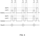
- FIG. 5 is a timing chart illustrating the waveforms of the control voltages Vmh1 and Vmh2.
- a first period of time T1 in which the control voltage Vmh1 and control voltage Vmh2 reach their respective predetermined levels at the same time and a second period of time T2 in which the control voltage Vmh1 and control voltage Vmh2 reach their respective predetermined levels at the same time are alternately repeated.
- the control voltage Vmh2 is set higher than the control voltage Vmh1, with the result that the heating temperature of the first thermistor Rd1 by the first heater resistor MH1 becomes, e.g., 150°C, and the heating temperature of the second thermistor Rd2 by the second heater resistor MH2 becomes, e.g., 300°C.
- the detection signal Vout1 is sampled by the control circuit 20, and the CO 2 gas concentration is determined based on the sampled signal.
- the sampling period of the Vout1 is, e.g., 30 sec.
- the control voltage Vmh1 is set higher than the control voltage Vmh2, with the result that the heating temperature of the first thermistor Rd1 by the first heater resistor MH1 becomes, e.g., 300°C, and the heating temperature of the second thermistor Rd2 by the second heater resistor MH2 becomes, e.g., 150°C.
- the control circuit 20 does not perform sampling of the detection signal Vout1.
- sampling of the detection signal Vout1 is not performed; however, a completely reverse temperature load to that in the first period of time T1 is applied to the first and second thermistors Rd1 and Rd2 to make the thermal histories of the first and second thermistors Rd1 and Rd2 coincide with each other. This makes it possible to easily and effectively suppress the temporal change of the gas sensor 10.
- FIG. 6 is a graph for explaining the effect of the present embodiment.
- the solid line denotes the temporal change of the gas sensor 10 according to the present embodiment
- the dashed line denotes the temporal change of the gas sensor 10 in a case where the heating operation in the second period of time T2 is omitted.
- the temporal change of the gas sensor 10 according to the present embodiment is significantly reduced as compared to when the heating operation in the second period of time T2 is omitted. This is because a completely reverse temperature load to that in the first period of time T1 is applied to the first and second thermistors Rd1 and Rd2 to make the thermal histories of the first and second thermistors Rd1 and Rd2 coincide with each other.
- the lengths of both the first and second periods of time T1 and T2 are preferably set in the range of 50 ms to 400 ms and are more preferably made to coincide with each other. That is, in the present embodiment, the first and second sensor parts S1 and S2 each have a MEMS structure, so that the time required from the start of heating by the first and second heater resistors MH1 and MH2 until the heating temperature of the first and second thermistors Rd1 and Rd2 is stabilized is about 50 ms. Further, heating beyond 400 ms, which may disadvantageously increase power consumption, is not required. Making the lengths of both the first and second periods of time T1 and T2 allows the thermal histories of the first and second thermistors Rd1 and Rd2 to completely coincide with each other.
- the timing at which the second period of time T2 is inserted is not limited unless the second period of time T2 does not overlap the first period of time T1.
- the second period of time T2 may be set immediately after the first period of time T1 so that they are continuous.
- the second period of time T2 may be inserted at a timing just corresponding to the midpoint between a given first period of time T1 and its subsequent first period of time T1.
- setting the second period of time T2 immediately before the first period of time T1 which may affect actual measurement due to residual heat in the second period of time T2, should preferably be avoided.
- first and second periods of time T1 and T2 need not be alternately repeated.
- the second period of time T2 may be inserted two times after two times of the first period of time T1.
Landscapes
- Chemical & Material Sciences (AREA)
- Health & Medical Sciences (AREA)
- Life Sciences & Earth Sciences (AREA)
- General Health & Medical Sciences (AREA)
- Immunology (AREA)
- Pathology (AREA)
- Analytical Chemistry (AREA)
- Biochemistry (AREA)
- Physics & Mathematics (AREA)
- General Physics & Mathematics (AREA)
- Chemical Kinetics & Catalysis (AREA)
- Electrochemistry (AREA)
- Engineering & Computer Science (AREA)
- Combustion & Propulsion (AREA)
- Food Science & Technology (AREA)
- Medicinal Chemistry (AREA)
- Investigating Or Analyzing Materials By The Use Of Electric Means (AREA)
Claims (6)
- Ein Gassensor, aufweisend:ein Detektionselement (Rd1), dessen Widerstandswert sich in Abhängigkeit von einer CO2-Konzentration ändert;ein Referenzelement (Rd2), das mit dem Detektionselement in Reihe geschaltet ist;ein erstes Heizelement (MH1) zum Beheizen des Detektionselements;ein zweites Heizelement (MH2) zum Beheizen des Referenzelements; undeine Steuerschaltung (20), die so konfiguriert ist, dass sie das erste und das zweite Heizelement so aufheizt, dass das Referenzelement in einer ersten Zeitspanne eine höhere Temperatur als das Detektionselement hat und dass das Detektionselement in einer zweiten Zeitspanne eine höhere Temperatur als das Referenzelement hat,wobei die Steuerschaltung so konfiguriert ist, dass sie das erste und das zweite Heizelement so aufheizt, dass das Detektionselement und das Referenzelement in der ersten Zeitspanne eine erste Temperatur bzw. eine zweite Temperatur aufweisen und dass das Referenzelement und das Detektionselement in der zweiten Zeitspanne die erste Temperatur bzw. die zweite Temperatur aufweisen;wobei die Heiztemperatur des Detektionselements in der ersten Zeitspanne in einem Bereich von 100° C bis 200° liegt; undwobei die Heiztemperatur des Referenzelements in der ersten Zeitspanne in einem Bereich von 250° C bis 350° C liegt.
- Gassensor nach Anspruch 1, wobei die Steuerschaltung so konfiguriert ist, dass sie die CO2 Gas-Konzentration auf der Grundlage eines Potenzials berechnet, das an einem Verbindungspunkt zwischen dem Detektionselement und dem Referenzelement in einer der ersten und zweiten Zeitspanne auftritt.
- Gassensor nach Anspruch 1 oder 2, wobei die Längen der ersten und der zweiten Zeitspanne einander gleich sind.
- Der Gassensor nach einem der Ansprüche 1 bis 3,wobei das Detektionselement und das Referenzelement eine MEMS-Struktur aufweisen, undwobei die Länge der ersten Zeitspanne in einem Bereich von 50 ms bis 400 ms liegt.
- Gassensor nach einem der Ansprüche 1 bis 4, wobei das Verhältnis zwischen dem Widerstandswert des Detektionselements und dem Widerstandswert des Referenzelements in der ersten Zeitspanne im Bereich von 0,5 bis 2,0 liegt.
- Gassensor nach einem der Ansprüche 1 bis 5, wobei das Detektionselement und das Referenzelement auf voneinander verschiedenen Chips ausgebildet sind.
Applications Claiming Priority (2)
| Application Number | Priority Date | Filing Date | Title |
|---|---|---|---|
| JP2018151364 | 2018-08-10 | ||
| PCT/JP2019/024432 WO2020031517A1 (ja) | 2018-08-10 | 2019-06-20 | ガスセンサ |
Publications (3)
| Publication Number | Publication Date |
|---|---|
| EP3835774A1 EP3835774A1 (de) | 2021-06-16 |
| EP3835774A4 EP3835774A4 (de) | 2022-04-20 |
| EP3835774B1 true EP3835774B1 (de) | 2024-07-31 |
Family
ID=69415520
Family Applications (1)
| Application Number | Title | Priority Date | Filing Date |
|---|---|---|---|
| EP19847665.7A Active EP3835774B1 (de) | 2018-08-10 | 2019-06-20 | Gassensor |
Country Status (5)
| Country | Link |
|---|---|
| US (1) | US11567025B2 (de) |
| EP (1) | EP3835774B1 (de) |
| JP (1) | JP7188445B2 (de) |
| CN (1) | CN112585455B (de) |
| WO (1) | WO2020031517A1 (de) |
Families Citing this family (13)
| Publication number | Priority date | Publication date | Assignee | Title |
|---|---|---|---|---|
| CN113196046B (zh) * | 2018-12-17 | 2024-03-08 | Tdk株式会社 | 气体传感器 |
| JP7287344B2 (ja) * | 2020-05-13 | 2023-06-06 | Tdk株式会社 | ガスセンサ |
| DE102022107394A1 (de) * | 2021-03-30 | 2022-10-06 | Tdk Electronics Ag | Sensorsystem, Sensoranordnung und Verfahren zur Verwendung des Sensorsystems |
| CN113671000A (zh) * | 2021-07-27 | 2021-11-19 | 浙江华才检测技术有限公司 | 基于半导体功能材料搭建的矩阵式广谱性物质检测传感器 |
| JP7785497B2 (ja) * | 2021-10-08 | 2025-12-15 | Tdk株式会社 | ガスセンサ |
| JP7821603B2 (ja) * | 2021-12-20 | 2026-02-27 | Tdk株式会社 | ガスセンサ |
| JP7803825B2 (ja) * | 2022-09-07 | 2026-01-21 | 株式会社東芝 | センサ及びガス変換システム |
| CN120225870A (zh) * | 2022-11-18 | 2025-06-27 | Tdk株式会社 | 气体传感器 |
| WO2024111024A1 (ja) * | 2022-11-21 | 2024-05-30 | Tdk株式会社 | ガスセンサ |
| JPWO2024116267A1 (de) * | 2022-11-29 | 2024-06-06 | ||
| WO2024116376A1 (ja) * | 2022-12-01 | 2024-06-06 | Tdk株式会社 | ガスセンサ |
| EP4502585A1 (de) * | 2023-07-31 | 2025-02-05 | Flusso Limited | Wärmeleitfähigkeitssensor zur messung einer konzentration eines gases |
| EP4644895A1 (de) * | 2024-05-03 | 2025-11-05 | Flusso Limited | Umgebungssensoranordnung |
Family Cites Families (40)
| Publication number | Priority date | Publication date | Assignee | Title |
|---|---|---|---|---|
| EP0376721B1 (de) * | 1988-12-29 | 1998-07-15 | Sharp Kabushiki Kaisha | Détecteur d'humidité |
| JP2815125B2 (ja) * | 1991-07-31 | 1998-10-27 | 新コスモス電機株式会社 | 接触燃焼式ガス検知素子 |
| US5297419A (en) * | 1992-07-16 | 1994-03-29 | Thermco Instrument Corporation | Linearizing gas analyzer |
| US5551283A (en) * | 1993-08-10 | 1996-09-03 | Ricoh Seiki Company, Ltd. | Atmosphere measuring device and flow sensor |
| US6019505A (en) * | 1997-12-31 | 2000-02-01 | Honeywell Inc. | Time lag approach for measuring thermal conductivity and specific heat |
| IT1312311B1 (it) * | 1999-05-07 | 2002-04-15 | Thermoquest Italia Spa | Dispositivo per la misurazione della conducibilita' termica di unfluido |
| JP3385248B2 (ja) * | 1999-10-29 | 2003-03-10 | 光明理化学工業株式会社 | ガスセンサ |
| US6724194B1 (en) * | 2000-06-30 | 2004-04-20 | Ballard Power Systems Inc. | Cell voltage monitor for a fuel cell stack |
| US6474138B1 (en) * | 2000-11-28 | 2002-11-05 | Honeywell International Inc. | Adsorption based carbon monoxide sensor and method |
| JP2002207024A (ja) * | 2001-01-05 | 2002-07-26 | Ngk Spark Plug Co Ltd | Coセンサ及びco濃度測定方法 |
| DE10146321B4 (de) * | 2001-09-20 | 2008-08-14 | Robert Bosch Gmbh | Sensorbaustein mit einem Sensorelement, das von einem Heizelement umgeben ist |
| JP2005351847A (ja) * | 2004-06-14 | 2005-12-22 | Jasco Corp | サーミスタ式温度計、及びペルチェ式セルチェンジャ |
| JP4692026B2 (ja) * | 2005-03-08 | 2011-06-01 | パナソニック株式会社 | ガスセンサ |
| US7628907B2 (en) * | 2005-08-26 | 2009-12-08 | Honeywell International Inc. | Gas sensor |
| JP4294633B2 (ja) * | 2005-10-28 | 2009-07-15 | パナソニックエコシステムズ株式会社 | ガス検出装置 |
| EP1790979A1 (de) * | 2005-11-24 | 2007-05-30 | Consultatie Implementatie Technisch Beheer B.V. | Elektronischer Detektor für chemische Spuren |
| US7972865B2 (en) | 2008-08-26 | 2011-07-05 | Ut-Battelle, Llc | Sensor for detecting and differentiating chemical analytes |
| US8467977B2 (en) * | 2010-07-29 | 2013-06-18 | General Electric Company | Fiber optic carbon dioxide purity sensor package and system |
| JP5563507B2 (ja) * | 2011-03-28 | 2014-07-30 | 日本特殊陶業株式会社 | ガス検出装置 |
| JP5986833B2 (ja) * | 2012-07-17 | 2016-09-06 | 日本特殊陶業株式会社 | 可燃性ガス検出装置 |
| CN203572531U (zh) * | 2013-11-27 | 2014-04-30 | 厦门市凯讯科技有限公司 | 一种热式气体质量流量计 |
| CN104731128A (zh) * | 2013-12-24 | 2015-06-24 | 苏州普源精电科技有限公司 | 一种具有温度控制功能的测量装置 |
| EP2889612A1 (de) * | 2013-12-24 | 2015-07-01 | Honeywell International Inc. | CO2-Sensor auf Grundlage eines Diamantfeldeffekttransistors |
| JP2015227822A (ja) * | 2014-06-02 | 2015-12-17 | Tdk株式会社 | 熱伝導式ガスセンサ |
| JP6119701B2 (ja) * | 2014-08-29 | 2017-04-26 | Tdk株式会社 | ガスセンサ |
| JP2016109527A (ja) | 2014-12-05 | 2016-06-20 | ヤマハファインテック株式会社 | 接触燃焼式ガスセンサ |
| JP2016133404A (ja) * | 2015-01-20 | 2016-07-25 | Tdk株式会社 | ガス検出装置 |
| WO2017051430A2 (en) * | 2015-03-05 | 2017-03-30 | Nanosniff Technologies Pvt. Ltd. | System and method of detecting explosive compounds based on rapid deflagration and differential micro-calorimetry |
| EP3093659B1 (de) * | 2015-05-11 | 2017-06-14 | Siemens Aktiengesellschaft | Wärmeleitfähigkeitsdetektor und verfahren zum betrieb davon |
| JP6499566B2 (ja) * | 2015-11-27 | 2019-04-10 | 日立オートモティブシステムズ株式会社 | 気体センサ装置及び気体センサ装置の加熱電流制御方法 |
| JP6679993B2 (ja) | 2016-03-04 | 2020-04-15 | Tdk株式会社 | ガス検出装置 |
| JP2017166826A (ja) * | 2016-03-14 | 2017-09-21 | Tdk株式会社 | ガスセンサ |
| JP6603633B2 (ja) * | 2016-08-22 | 2019-11-06 | 日立オートモティブシステムズ株式会社 | センサ装置 |
| JP6802703B2 (ja) * | 2016-12-14 | 2020-12-16 | 日立オートモティブシステムズ株式会社 | 気体センサ装置 |
| WO2018135100A1 (ja) * | 2017-01-19 | 2018-07-26 | Tdk株式会社 | ガスセンサ |
| US10598621B2 (en) * | 2017-04-11 | 2020-03-24 | Invensense, Inc. | Gas sensing device with chemical and thermal conductivity sensing |
| DE102017215527A1 (de) * | 2017-09-05 | 2019-03-07 | Robert Bosch Gmbh | Gassensor zum Messen einer Konzentration eines Analysegases |
| US11275043B2 (en) * | 2017-10-10 | 2022-03-15 | Indian Institute Of Science | Nano-sensor for detecting gaseous components |
| US10883947B2 (en) * | 2017-11-01 | 2021-01-05 | Palo Alto Research Center Incorporated | Sorbent based gas concentration monitor |
| CA3087304C (en) * | 2017-12-30 | 2024-04-30 | Mark Alan Lemkin | Cannabinoid processing system and method |
-
2019
- 2019-06-20 WO PCT/JP2019/024432 patent/WO2020031517A1/ja not_active Ceased
- 2019-06-20 US US17/265,958 patent/US11567025B2/en active Active
- 2019-06-20 JP JP2020536367A patent/JP7188445B2/ja active Active
- 2019-06-20 EP EP19847665.7A patent/EP3835774B1/de active Active
- 2019-06-20 CN CN201980053750.6A patent/CN112585455B/zh active Active
Also Published As
| Publication number | Publication date |
|---|---|
| US20210293735A1 (en) | 2021-09-23 |
| EP3835774A4 (de) | 2022-04-20 |
| US11567025B2 (en) | 2023-01-31 |
| JPWO2020031517A1 (ja) | 2021-08-10 |
| CN112585455A (zh) | 2021-03-30 |
| EP3835774A1 (de) | 2021-06-16 |
| WO2020031517A1 (ja) | 2020-02-13 |
| CN112585455B (zh) | 2024-10-29 |
| JP7188445B2 (ja) | 2022-12-13 |
Similar Documents
| Publication | Publication Date | Title |
|---|---|---|
| EP3835774B1 (de) | Gassensor | |
| EP3690432B1 (de) | Gassensor | |
| US11408843B2 (en) | Gas sensor | |
| US11898980B2 (en) | Gas sensor | |
| JP6160667B2 (ja) | 熱伝導式ガスセンサ | |
| JP6679993B2 (ja) | ガス検出装置 | |
| RU2248538C2 (ru) | Высокотемпературные схемные структуры | |
| JP6879060B2 (ja) | ガスセンサ | |
| JP2017166826A (ja) | ガスセンサ | |
| JP6631049B2 (ja) | ガス検出装置 | |
| JP2009168649A (ja) | 傍熱型感温抵抗素子、及び傍熱型感温抵抗素子を用いた絶対湿度センサ | |
| WO2019065127A1 (ja) | ガスセンサ | |
| JP2015227822A (ja) | 熱伝導式ガスセンサ | |
| JP6729197B2 (ja) | ガスセンサ | |
| JP6119701B2 (ja) | ガスセンサ | |
| JP7314791B2 (ja) | ガスセンサ | |
| JP7156014B2 (ja) | サーミスタ及びこれを備えるガスセンサ | |
| US20250258121A1 (en) | Gas sensor |
Legal Events
| Date | Code | Title | Description |
|---|---|---|---|
| STAA | Information on the status of an ep patent application or granted ep patent |
Free format text: STATUS: THE INTERNATIONAL PUBLICATION HAS BEEN MADE |
|
| PUAI | Public reference made under article 153(3) epc to a published international application that has entered the european phase |
Free format text: ORIGINAL CODE: 0009012 |
|
| STAA | Information on the status of an ep patent application or granted ep patent |
Free format text: STATUS: REQUEST FOR EXAMINATION WAS MADE |
|
| 17P | Request for examination filed |
Effective date: 20210202 |
|
| AK | Designated contracting states |
Kind code of ref document: A1 Designated state(s): AL AT BE BG CH CY CZ DE DK EE ES FI FR GB GR HR HU IE IS IT LI LT LU LV MC MK MT NL NO PL PT RO RS SE SI SK SM TR |
|
| DAV | Request for validation of the european patent (deleted) | ||
| DAX | Request for extension of the european patent (deleted) | ||
| A4 | Supplementary search report drawn up and despatched |
Effective date: 20220318 |
|
| RIC1 | Information provided on ipc code assigned before grant |
Ipc: G01N 27/18 20060101AFI20220314BHEP |
|
| GRAP | Despatch of communication of intention to grant a patent |
Free format text: ORIGINAL CODE: EPIDOSNIGR1 |
|
| STAA | Information on the status of an ep patent application or granted ep patent |
Free format text: STATUS: GRANT OF PATENT IS INTENDED |
|
| INTG | Intention to grant announced |
Effective date: 20240321 |
|
| GRAS | Grant fee paid |
Free format text: ORIGINAL CODE: EPIDOSNIGR3 |
|
| GRAA | (expected) grant |
Free format text: ORIGINAL CODE: 0009210 |
|
| STAA | Information on the status of an ep patent application or granted ep patent |
Free format text: STATUS: THE PATENT HAS BEEN GRANTED |
|
| AK | Designated contracting states |
Kind code of ref document: B1 Designated state(s): AL AT BE BG CH CY CZ DE DK EE ES FI FR GB GR HR HU IE IS IT LI LT LU LV MC MK MT NL NO PL PT RO RS SE SI SK SM TR |
|
| REG | Reference to a national code |
Ref country code: CH Ref legal event code: EP Ref country code: GB Ref legal event code: FG4D |
|
| REG | Reference to a national code |
Ref country code: DE Ref legal event code: R096 Ref document number: 602019056275 Country of ref document: DE |
|
| REG | Reference to a national code |
Ref country code: IE Ref legal event code: FG4D |
|
| REG | Reference to a national code |
Ref country code: LT Ref legal event code: MG9D |
|
| REG | Reference to a national code |
Ref country code: NL Ref legal event code: MP Effective date: 20240731 |
|
| PG25 | Lapsed in a contracting state [announced via postgrant information from national office to epo] |
Ref country code: PT Free format text: LAPSE BECAUSE OF FAILURE TO SUBMIT A TRANSLATION OF THE DESCRIPTION OR TO PAY THE FEE WITHIN THE PRESCRIBED TIME-LIMIT Effective date: 20241202 |
|
| REG | Reference to a national code |
Ref country code: AT Ref legal event code: MK05 Ref document number: 1708920 Country of ref document: AT Kind code of ref document: T Effective date: 20240731 |
|
| PG25 | Lapsed in a contracting state [announced via postgrant information from national office to epo] |
Ref country code: PT Free format text: LAPSE BECAUSE OF FAILURE TO SUBMIT A TRANSLATION OF THE DESCRIPTION OR TO PAY THE FEE WITHIN THE PRESCRIBED TIME-LIMIT Effective date: 20241202 |
|
| PG25 | Lapsed in a contracting state [announced via postgrant information from national office to epo] |
Ref country code: NO Free format text: LAPSE BECAUSE OF FAILURE TO SUBMIT A TRANSLATION OF THE DESCRIPTION OR TO PAY THE FEE WITHIN THE PRESCRIBED TIME-LIMIT Effective date: 20241031 |
|
| PG25 | Lapsed in a contracting state [announced via postgrant information from national office to epo] |
Ref country code: NL Free format text: LAPSE BECAUSE OF FAILURE TO SUBMIT A TRANSLATION OF THE DESCRIPTION OR TO PAY THE FEE WITHIN THE PRESCRIBED TIME-LIMIT Effective date: 20240731 Ref country code: FI Free format text: LAPSE BECAUSE OF FAILURE TO SUBMIT A TRANSLATION OF THE DESCRIPTION OR TO PAY THE FEE WITHIN THE PRESCRIBED TIME-LIMIT Effective date: 20240731 Ref country code: GR Free format text: LAPSE BECAUSE OF FAILURE TO SUBMIT A TRANSLATION OF THE DESCRIPTION OR TO PAY THE FEE WITHIN THE PRESCRIBED TIME-LIMIT Effective date: 20241101 Ref country code: PL Free format text: LAPSE BECAUSE OF FAILURE TO SUBMIT A TRANSLATION OF THE DESCRIPTION OR TO PAY THE FEE WITHIN THE PRESCRIBED TIME-LIMIT Effective date: 20240731 |
|
| PG25 | Lapsed in a contracting state [announced via postgrant information from national office to epo] |
Ref country code: BG Free format text: LAPSE BECAUSE OF FAILURE TO SUBMIT A TRANSLATION OF THE DESCRIPTION OR TO PAY THE FEE WITHIN THE PRESCRIBED TIME-LIMIT Effective date: 20240731 |
|
| PG25 | Lapsed in a contracting state [announced via postgrant information from national office to epo] |
Ref country code: LV Free format text: LAPSE BECAUSE OF FAILURE TO SUBMIT A TRANSLATION OF THE DESCRIPTION OR TO PAY THE FEE WITHIN THE PRESCRIBED TIME-LIMIT Effective date: 20240731 |
|
| PG25 | Lapsed in a contracting state [announced via postgrant information from national office to epo] |
Ref country code: AT Free format text: LAPSE BECAUSE OF FAILURE TO SUBMIT A TRANSLATION OF THE DESCRIPTION OR TO PAY THE FEE WITHIN THE PRESCRIBED TIME-LIMIT Effective date: 20240731 Ref country code: IS Free format text: LAPSE BECAUSE OF FAILURE TO SUBMIT A TRANSLATION OF THE DESCRIPTION OR TO PAY THE FEE WITHIN THE PRESCRIBED TIME-LIMIT Effective date: 20241130 |
|
| PG25 | Lapsed in a contracting state [announced via postgrant information from national office to epo] |
Ref country code: HR Free format text: LAPSE BECAUSE OF FAILURE TO SUBMIT A TRANSLATION OF THE DESCRIPTION OR TO PAY THE FEE WITHIN THE PRESCRIBED TIME-LIMIT Effective date: 20240731 |
|
| PG25 | Lapsed in a contracting state [announced via postgrant information from national office to epo] |
Ref country code: ES Free format text: LAPSE BECAUSE OF FAILURE TO SUBMIT A TRANSLATION OF THE DESCRIPTION OR TO PAY THE FEE WITHIN THE PRESCRIBED TIME-LIMIT Effective date: 20240731 Ref country code: RS Free format text: LAPSE BECAUSE OF FAILURE TO SUBMIT A TRANSLATION OF THE DESCRIPTION OR TO PAY THE FEE WITHIN THE PRESCRIBED TIME-LIMIT Effective date: 20241031 |
|
| PG25 | Lapsed in a contracting state [announced via postgrant information from national office to epo] |
Ref country code: RS Free format text: LAPSE BECAUSE OF FAILURE TO SUBMIT A TRANSLATION OF THE DESCRIPTION OR TO PAY THE FEE WITHIN THE PRESCRIBED TIME-LIMIT Effective date: 20241031 Ref country code: PL Free format text: LAPSE BECAUSE OF FAILURE TO SUBMIT A TRANSLATION OF THE DESCRIPTION OR TO PAY THE FEE WITHIN THE PRESCRIBED TIME-LIMIT Effective date: 20240731 Ref country code: NO Free format text: LAPSE BECAUSE OF FAILURE TO SUBMIT A TRANSLATION OF THE DESCRIPTION OR TO PAY THE FEE WITHIN THE PRESCRIBED TIME-LIMIT Effective date: 20241031 Ref country code: NL Free format text: LAPSE BECAUSE OF FAILURE TO SUBMIT A TRANSLATION OF THE DESCRIPTION OR TO PAY THE FEE WITHIN THE PRESCRIBED TIME-LIMIT Effective date: 20240731 Ref country code: LV Free format text: LAPSE BECAUSE OF FAILURE TO SUBMIT A TRANSLATION OF THE DESCRIPTION OR TO PAY THE FEE WITHIN THE PRESCRIBED TIME-LIMIT Effective date: 20240731 Ref country code: IS Free format text: LAPSE BECAUSE OF FAILURE TO SUBMIT A TRANSLATION OF THE DESCRIPTION OR TO PAY THE FEE WITHIN THE PRESCRIBED TIME-LIMIT Effective date: 20241130 Ref country code: HR Free format text: LAPSE BECAUSE OF FAILURE TO SUBMIT A TRANSLATION OF THE DESCRIPTION OR TO PAY THE FEE WITHIN THE PRESCRIBED TIME-LIMIT Effective date: 20240731 Ref country code: GR Free format text: LAPSE BECAUSE OF FAILURE TO SUBMIT A TRANSLATION OF THE DESCRIPTION OR TO PAY THE FEE WITHIN THE PRESCRIBED TIME-LIMIT Effective date: 20241101 Ref country code: FI Free format text: LAPSE BECAUSE OF FAILURE TO SUBMIT A TRANSLATION OF THE DESCRIPTION OR TO PAY THE FEE WITHIN THE PRESCRIBED TIME-LIMIT Effective date: 20240731 Ref country code: ES Free format text: LAPSE BECAUSE OF FAILURE TO SUBMIT A TRANSLATION OF THE DESCRIPTION OR TO PAY THE FEE WITHIN THE PRESCRIBED TIME-LIMIT Effective date: 20240731 Ref country code: BG Free format text: LAPSE BECAUSE OF FAILURE TO SUBMIT A TRANSLATION OF THE DESCRIPTION OR TO PAY THE FEE WITHIN THE PRESCRIBED TIME-LIMIT Effective date: 20240731 Ref country code: AT Free format text: LAPSE BECAUSE OF FAILURE TO SUBMIT A TRANSLATION OF THE DESCRIPTION OR TO PAY THE FEE WITHIN THE PRESCRIBED TIME-LIMIT Effective date: 20240731 |
|
| PG25 | Lapsed in a contracting state [announced via postgrant information from national office to epo] |
Ref country code: DK Free format text: LAPSE BECAUSE OF FAILURE TO SUBMIT A TRANSLATION OF THE DESCRIPTION OR TO PAY THE FEE WITHIN THE PRESCRIBED TIME-LIMIT Effective date: 20240731 Ref country code: SM Free format text: LAPSE BECAUSE OF FAILURE TO SUBMIT A TRANSLATION OF THE DESCRIPTION OR TO PAY THE FEE WITHIN THE PRESCRIBED TIME-LIMIT Effective date: 20240731 Ref country code: RO Free format text: LAPSE BECAUSE OF FAILURE TO SUBMIT A TRANSLATION OF THE DESCRIPTION OR TO PAY THE FEE WITHIN THE PRESCRIBED TIME-LIMIT Effective date: 20240731 |
|
| PG25 | Lapsed in a contracting state [announced via postgrant information from national office to epo] |
Ref country code: EE Free format text: LAPSE BECAUSE OF FAILURE TO SUBMIT A TRANSLATION OF THE DESCRIPTION OR TO PAY THE FEE WITHIN THE PRESCRIBED TIME-LIMIT Effective date: 20240731 |
|
| PG25 | Lapsed in a contracting state [announced via postgrant information from national office to epo] |
Ref country code: CZ Free format text: LAPSE BECAUSE OF FAILURE TO SUBMIT A TRANSLATION OF THE DESCRIPTION OR TO PAY THE FEE WITHIN THE PRESCRIBED TIME-LIMIT Effective date: 20240731 |
|
| PG25 | Lapsed in a contracting state [announced via postgrant information from national office to epo] |
Ref country code: IT Free format text: LAPSE BECAUSE OF FAILURE TO SUBMIT A TRANSLATION OF THE DESCRIPTION OR TO PAY THE FEE WITHIN THE PRESCRIBED TIME-LIMIT Effective date: 20240731 Ref country code: SK Free format text: LAPSE BECAUSE OF FAILURE TO SUBMIT A TRANSLATION OF THE DESCRIPTION OR TO PAY THE FEE WITHIN THE PRESCRIBED TIME-LIMIT Effective date: 20240731 |
|
| REG | Reference to a national code |
Ref country code: DE Ref legal event code: R097 Ref document number: 602019056275 Country of ref document: DE |
|
| PLBE | No opposition filed within time limit |
Free format text: ORIGINAL CODE: 0009261 |
|
| STAA | Information on the status of an ep patent application or granted ep patent |
Free format text: STATUS: NO OPPOSITION FILED WITHIN TIME LIMIT |
|
| 26N | No opposition filed |
Effective date: 20250501 |
|
| PGFP | Annual fee paid to national office [announced via postgrant information from national office to epo] |
Ref country code: DE Payment date: 20250624 Year of fee payment: 7 |
|
| PG25 | Lapsed in a contracting state [announced via postgrant information from national office to epo] |
Ref country code: SE Free format text: LAPSE BECAUSE OF FAILURE TO SUBMIT A TRANSLATION OF THE DESCRIPTION OR TO PAY THE FEE WITHIN THE PRESCRIBED TIME-LIMIT Effective date: 20240731 |
|
| REG | Reference to a national code |
Ref country code: CH Ref legal event code: H13 Free format text: ST27 STATUS EVENT CODE: U-0-0-H10-H13 (AS PROVIDED BY THE NATIONAL OFFICE) Effective date: 20260127 |
|
| PG25 | Lapsed in a contracting state [announced via postgrant information from national office to epo] |
Ref country code: MC Free format text: LAPSE BECAUSE OF FAILURE TO SUBMIT A TRANSLATION OF THE DESCRIPTION OR TO PAY THE FEE WITHIN THE PRESCRIBED TIME-LIMIT Effective date: 20240731 |
|
| PG25 | Lapsed in a contracting state [announced via postgrant information from national office to epo] |
Ref country code: LU Free format text: LAPSE BECAUSE OF NON-PAYMENT OF DUE FEES Effective date: 20250620 |
|
| GBPC | Gb: european patent ceased through non-payment of renewal fee |
Effective date: 20250620 |
|
| REG | Reference to a national code |
Ref country code: BE Ref legal event code: MM Effective date: 20250630 |
|
| PG25 | Lapsed in a contracting state [announced via postgrant information from national office to epo] |
Ref country code: GB Free format text: LAPSE BECAUSE OF NON-PAYMENT OF DUE FEES Effective date: 20250620 |
|
| PG25 | Lapsed in a contracting state [announced via postgrant information from national office to epo] |
Ref country code: IE Free format text: LAPSE BECAUSE OF NON-PAYMENT OF DUE FEES Effective date: 20250620 |
|
| PG25 | Lapsed in a contracting state [announced via postgrant information from national office to epo] |
Ref country code: BE Free format text: LAPSE BECAUSE OF NON-PAYMENT OF DUE FEES Effective date: 20250630 |
|
| PG25 | Lapsed in a contracting state [announced via postgrant information from national office to epo] |
Ref country code: FR Free format text: LAPSE BECAUSE OF NON-PAYMENT OF DUE FEES Effective date: 20250630 |
|
| PG25 | Lapsed in a contracting state [announced via postgrant information from national office to epo] |
Ref country code: CH Free format text: LAPSE BECAUSE OF NON-PAYMENT OF DUE FEES Effective date: 20250630 |