EP3836765A1 - Elektrisches isolationsmodul für elektrische hochspannungsausstattung - Google Patents
Elektrisches isolationsmodul für elektrische hochspannungsausstattung Download PDFInfo
- Publication number
- EP3836765A1 EP3836765A1 EP20210388.3A EP20210388A EP3836765A1 EP 3836765 A1 EP3836765 A1 EP 3836765A1 EP 20210388 A EP20210388 A EP 20210388A EP 3836765 A1 EP3836765 A1 EP 3836765A1
- Authority
- EP
- European Patent Office
- Prior art keywords
- electrical
- peripheral wall
- electrical component
- housing
- wall
- Prior art date
- Legal status (The legal status is an assumption and is not a legal conclusion. Google has not performed a legal analysis and makes no representation as to the accuracy of the status listed.)
- Granted
Links
Images


Classifications
-
- H—ELECTRICITY
- H05—ELECTRIC TECHNIQUES NOT OTHERWISE PROVIDED FOR
- H05K—PRINTED CIRCUITS; CASINGS OR CONSTRUCTIONAL DETAILS OF ELECTRIC APPARATUS; MANUFACTURE OF ASSEMBLAGES OF ELECTRICAL COMPONENTS
- H05K7/00—Constructional details common to different types of electric apparatus
- H05K7/14—Mounting supporting structure in casing or on frame or rack
- H05K7/1422—Printed circuit boards receptacles, e.g. stacked structures, electronic circuit modules or box like frames
- H05K7/1427—Housings
- H05K7/1432—Housings specially adapted for power drive units or power converters
- H05K7/14339—Housings specially adapted for power drive units or power converters specially adapted for high voltage operation
-
- H—ELECTRICITY
- H02—GENERATION; CONVERSION OR DISTRIBUTION OF ELECTRIC POWER
- H02B—BOARDS, SUBSTATIONS OR SWITCHING ARRANGEMENTS FOR THE SUPPLY OR DISTRIBUTION OF ELECTRIC POWER
- H02B1/00—Frameworks, boards, panels, desks, casings; Details of substations or switching arrangements
- H02B1/26—Casings; Parts thereof or accessories therefor
-
- H—ELECTRICITY
- H05—ELECTRIC TECHNIQUES NOT OTHERWISE PROVIDED FOR
- H05K—PRINTED CIRCUITS; CASINGS OR CONSTRUCTIONAL DETAILS OF ELECTRIC APPARATUS; MANUFACTURE OF ASSEMBLAGES OF ELECTRICAL COMPONENTS
- H05K7/00—Constructional details common to different types of electric apparatus
- H05K7/02—Arrangements of circuit components or wiring on supporting structure
- H05K7/12—Resilient or clamping means for holding component to structure
-
- H—ELECTRICITY
- H02—GENERATION; CONVERSION OR DISTRIBUTION OF ELECTRIC POWER
- H02B—BOARDS, SUBSTATIONS OR SWITCHING ARRANGEMENTS FOR THE SUPPLY OR DISTRIBUTION OF ELECTRIC POWER
- H02B1/00—Frameworks, boards, panels, desks, casings; Details of substations or switching arrangements
- H02B1/14—Shutters or guards for preventing access to contacts
-
- H—ELECTRICITY
- H02—GENERATION; CONVERSION OR DISTRIBUTION OF ELECTRIC POWER
- H02M—APPARATUS FOR CONVERSION BETWEEN AC AND AC, BETWEEN AC AND DC, OR BETWEEN DC AND DC, AND FOR USE WITH MAINS OR SIMILAR POWER SUPPLY SYSTEMS; CONVERSION OF DC OR AC INPUT POWER INTO SURGE OUTPUT POWER; CONTROL OR REGULATION THEREOF
- H02M7/00—Conversion of AC power input into DC power output; Conversion of DC power input into AC power output
- H02M7/003—Constructional details, e.g. physical layout, assembly, wiring or busbar connections
-
- H—ELECTRICITY
- H05—ELECTRIC TECHNIQUES NOT OTHERWISE PROVIDED FOR
- H05K—PRINTED CIRCUITS; CASINGS OR CONSTRUCTIONAL DETAILS OF ELECTRIC APPARATUS; MANUFACTURE OF ASSEMBLAGES OF ELECTRICAL COMPONENTS
- H05K5/00—Casings, cabinets or drawers for electric apparatus
- H05K5/02—Details
- H05K5/0217—Mechanical details of casings
-
- H—ELECTRICITY
- H05—ELECTRIC TECHNIQUES NOT OTHERWISE PROVIDED FOR
- H05K—PRINTED CIRCUITS; CASINGS OR CONSTRUCTIONAL DETAILS OF ELECTRIC APPARATUS; MANUFACTURE OF ASSEMBLAGES OF ELECTRICAL COMPONENTS
- H05K5/00—Casings, cabinets or drawers for electric apparatus
- H05K5/02—Details
- H05K5/0247—Electrical details of casings, e.g. terminals, passages for cables or wiring
-
- H—ELECTRICITY
- H05—ELECTRIC TECHNIQUES NOT OTHERWISE PROVIDED FOR
- H05K—PRINTED CIRCUITS; CASINGS OR CONSTRUCTIONAL DETAILS OF ELECTRIC APPARATUS; MANUFACTURE OF ASSEMBLAGES OF ELECTRICAL COMPONENTS
- H05K5/00—Casings, cabinets or drawers for electric apparatus
- H05K5/10—Casings, cabinets or drawers for electric apparatus comprising several parts forming a closed casing
-
- H—ELECTRICITY
- H05—ELECTRIC TECHNIQUES NOT OTHERWISE PROVIDED FOR
- H05K—PRINTED CIRCUITS; CASINGS OR CONSTRUCTIONAL DETAILS OF ELECTRIC APPARATUS; MANUFACTURE OF ASSEMBLAGES OF ELECTRICAL COMPONENTS
- H05K7/00—Constructional details common to different types of electric apparatus
- H05K7/20—Modifications to facilitate cooling, ventilating, or heating
- H05K7/2089—Modifications to facilitate cooling, ventilating, or heating for power electronics, e.g. for inverters for controlling motor
- H05K7/209—Heat transfer by conduction from internal heat source to heat radiating structure
Definitions
- the present invention relates, in general, to the field of electrical equipment.
- the invention relates more particularly to high voltage electrical equipment for electric or hybrid vehicles.
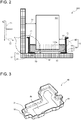
- Electrical equipment of an electric or hybrid vehicle such as an inverter of an electric vehicle, comprises electrical components housed in a housing of the electrical equipment, as illustrated in figure 1 .
- the figure 1 illustrates the longitudinal section of an electrical equipment 100 comprising a housing 112 and an electrical component 111.
- the electrical component 111 is for example, like the housing 112, an electrically conductive object.
- the electrical component 111 can comprise an insulating outer casing which is liable to present a fault. Such a fault possibly causes a leakage current between the electrical component 111 and the housing 112.
- the electrical equipment generally includes a thermal pad 66.
- the thermal pad 66 is placed between the base plate 115 of the housing 112 and the electrical component 111.
- the thermal pad 66 is of an insulating material and has thermal conductivity allowing heat dissipation between the electrical component 111 and the base plate 115.
- the minimum distance between the electrical component 111 and the side wall 116 must be a distance greater than this electrical safety distance 131, so as to ensure that, during the use of the l electrical equipment 100, there is no possibility of breaking the electrical insulation through the air.
- the difference in electrical potential between the housing 112 and the electrical component 111, in particular between the base wall 115 and the electrical component 111 determines a leakage line 170.
- the leakage line 170 is determined as the resistance path. weaker followed by an electric current of parasitic surface between the electric component 111 and the housing 112, in particular between the electric component 111 and the base plate 115.
- the creepage line 170 extends in particular along the outer surface of the heat pad 66 between the electrical component 111 and the base plate 115.
- the creepage line 170 follows the contour of the heat pad 66 before touching the base plate 115.
- the creepage line 170 should be long enough so that it A parasitic electric current between the electric component 111 and the housing 112 does not occur.
- the electrical component 111 of the electrical equipment 100 of the figure 1 is a high voltage electrical component (designated "High Voltage”, "HV” in English), said difference in electrical potential is too great for the leakage line 170 to be long enough to prevent the appearance of a leakage current. area. In this case, for the electrical equipment 100, it is very important to further extend the creepage line 170, while limiting the bulk in the electrical equipment 100.
- the present invention is aimed at an inexpensive solution which makes it possible to increase the length of the creepage line without increasing the size of electrical equipment.
- the present invention relates to an electrical insulation module configured to determine at least one leakage line between an electrical component and a housing receiving said electrical component.
- the electrical insulation module being made of an electrical insulating material, comprises a spacer configured to define the at least one leakage line between said electrical component and said housing.
- Said spacer comprises a bottom wall and a peripheral wall, in which the peripheral wall follows a direction different from that of the bottom wall, an internal angle being formed between the bottom wall and the peripheral wall; and the at least one creepage line comprises at least one dimension of a surface corresponding to a portion of the bottom wall and / or a dimension of a surface of a portion of the peripheral wall.
- the invention therefore makes it possible to increase the length of the creepage line without increasing the size of electrical equipment.
- said internal angle is between 80 and 110 degrees.
- said spacer comprises a receiving cavity defined by the bottom wall and the peripheral wall is configured to receive at least a portion of the at least one electrical component.
- the bottom wall is configured to receive said electrical component against it, and the peripheral wall is configured to come at least in part around said electrical component.
- the peripheral wall comprises a rim, the at least one creepage line further comprising a dimension of a surface of said rim.
- the peripheral wall is in contact with the bottom wall at a first end of the peripheral wall and the peripheral wall comprises a second end opposite the first end; said rim extending from the second end in a direction transverse to the peripheral wall.
- the electrical insulation module comprises a thermal pad configured to be positioned between said electrical component and said spacer, said thermal pad being configured to remove at least part of the heat generated during operation of the electrical component.
- the spacer comprises an opening formed in the bottom wall and configured to allow contact between the thermal pad and a wall of the housing so as to remove at least part of said heat generated.
- the thermal pad is made of a deformable material.
- the thermal pad is configured to deform when the electrical component is received in the receiving cavity, in particular against the bottom wall.
- the thermal cushion being interposed between said electrical component and said bottom wall. The thermal cushion is deformed in particular so as to pass through the opening in the bottom wall to come into contact with the wall of the housing.
- the present invention also relates to electrical equipment comprising a housing and at least one electrical component; said housing comprising at least one housing defined by a side wall and a support plate on which the at least one electrical component is mounted; the electrical equipment comprising an electrical isolation module as briefly described above.
- the electrical component is received in said receiving cavity of the electrical insulation module.
- a first line of flight extends successively along an upper external surface of the thermal cushion situated between the electrical component and the peripheral wall; and an internal surface of the peripheral wall devoid of the thermal pad.
- the peripheral wall of the spacer is in contact with the side wall of the case; and the first line of flight extends to the side wall of the housing.
- the peripheral wall of the spacer is at a distance from the side wall of the box; and the first creepage line extends along an outer surface of the peripheral wall of the spacer to said support plate.
- a first line of flight extends successively along an upper external surface of the thermal cushion situated between the electrical component and the peripheral wall; an internal surface of the peripheral wall devoid of the thermal cushion; and an outer surface of the peripheral wall to said support plate.
- a second line of flight extends successively along an upper external surface of the thermal cushion located between the electrical component and the peripheral wall; a first contact surface between the thermal pad and said peripheral wall; and a third contact surface between the thermal pad and said bottom wall up to said support plate.
- the at least one electrical component is a capacitive element or a coil or a capacitor or a transformer.
- said electrical equipment is an inverter or a DC-DC voltage converter or an electrical charger, in particular configured to be installed in a vehicle.
- the at least one electrical component is a high voltage electrical component.
- said support plate is a base plate of said housing, or an intermediate plate installed between a base plate and an opening of said housing.
- said side wall is orthogonal to said support plate, said side wall being a peripheral wall of said housing or a partition wall installed in said housing.
- the figure 2 illustrates the longitudinal section of an electrical insulation module 5, installed in electrical equipment 200, according to one embodiment of the invention.
- the electrical equipment 200 comprises a box, at least one electrical component 101, and the electrical insulation module 5.
- the example of the electrical equipment 200 illustrated in figure 2 comprises a single electrical component 101.
- the electrical insulation module 5 being made of an electrical insulating material, is configured to define at least one creepage line 71, 72 of the electrical equipment 200, the length of said at least one creepage line being increased with respect to l prior art.
- the electrical insulation module 5 will be described in more detail in the following paragraphs.
- the housing comprises at least one housing configured to house the at least one electrical component 101.
- the figure 2 describes such a housing 12.
- the housing 12 is defined by a side wall 16 and a support plate 15 on which the at least one electrical component 101 is mounted.
- the side wall 16 and the support plate 15 are respectively made of an electrically conductive material, such as a metallic material.
- said conductive material is a metal or a metal alloy, chosen for example from the following materials: aluminum, copper, aluminum alloy, copper-magnesium alloy.
- the housing of the electrical equipment 200 comprises a single housing.
- the support plate 15 is a base plate of said housing.
- the side wall 16 is a side wall of the housing.
- the housing comprises several housings. At least one of these housings, the side wall 16 of which and / or the support plate 15 are respectively a partition wall and / or an intermediate plate installed inside the box of the electrical equipment 200.
- Said partition wall is preferably parallel to the side wall of the housing.
- Said intermediate plate, installed between an upper opening of the housing and the base plate of the housing, is preferably parallel to the base plate of the housing.
- the thicknesses of the side wall 16 and of the support plate 15 are respectively 4 mm (millimeter) and 4 mm.
- the housing and the housing respectively have the shape of a rectangular parallelepiped.
- the housing and the housing may have another shape, for example a cylinder.
- the side wall 16 is preferably orthogonal to the support plate 15; that is, an internal angle between the support plate 15 and the side wall 16 is equal to 90 degrees. Alternatively, said internal angle may be between 80 and 110 degrees.
- the at least one electrical component 101 is configured to present an electrical potential.
- the electrical component 101 is for example a capacitive element, a coil, a capacitor, or a transformer.
- the electrical component 101 can be a high voltage electrical component. High voltage preferably designates a voltage greater than 60V (Volts) or even greater than 80V, or even greater than 100V.
- the electrical equipment 200 can be an inverter, a DC-to-DC voltage converter or an electrical charger, in particular configured to be installed in a vehicle.
- the electrical component 101 comprises an insulating envelope.
- the part of the electrical component 101 facing a bottom wall 51 of a spacer 50 (described in more detail below) and in contact with a thermal pad 60 (described in more detail below) is devoid of the insulating envelope in order to promote heat exchange.
- the part of the electrical component 101 facing the bottom wall 51 comprises in particular a thermal conductive part, in particular metallic.
- first spacing 31 between the side wall 16 of the housing 12 and the at least one electrical component 101.
- the first spacing 31 is advantageously between 0 mm and 10 mm.
- the length of the first spacing 31 is greater than or equal to a distance of electrical insulation by air.
- the second spacing 32 is advantageously between 0.5 mm and 5 mm.
- the second space 32 is largely filled by the thickness of the thermal pad 60.
- the electrical insulation module 5 comprises said spacer 50.
- the figures 3 and 4 illustrate, from two different perspectives, the spacer 50 according to one embodiment of the invention.
- the spacer 50 comprises said bottom wall 51, a peripheral wall 52 and a receiving cavity.
- the peripheral wall 52 preferably located between the at least one electrical component 101 and the side wall 16, follows a direction different from that of the first space 31.
- the bottom wall 51 and / or the peripheral wall 52 can be multiple. -thicknesses, that is to say having variable thicknesses.
- an internal angle 55 formed between the bottom wall 51 and the peripheral wall 52 is between 80 and 110 degrees.
- the peripheral wall 52 is preferably orthogonal to the bottom wall 51; i.e. said internal angle 55 being 90 degrees.
- the peripheral wall 52 preferably comprises a rim 58, in particular configured to allow the spacer 50 to be grasped and manipulated.
- the rim 58 is formed at a second end of the peripheral wall 52 which is distal with respect to a first end of the wall. peripheral 52 from which the bottom wall 51 extends.
- the spacer 50 is formed in one piece.
- the spacer 50 can be made by performing a stamping manufacturing process, and the flange 58 can therefore be imposed by a stamping process.
- the rim 58 is thus counted in the first leakage line 71, which therefore makes it possible to reduce the height of the spacer 50, in particular the distance between the first end of the peripheral wall 52 and the second end of the peripheral wall 52.
- Said receiving cavity defined by the bottom wall 51 and the peripheral wall 52, is configured to receive at least a portion 101a of the at least one electrical component 101, as for example illustrated in figure 2 .
- the spacer 50 is placed in the housing 12. More precisely, the spacer 50 is placed between the at least one electrical component 101 and the assembly of the support plate 15 and of the side wall 16.
- the third spacing 33 being in particular less than the first spacing 31.
- the third spacing 33 is advantageously between 0.5 mm and 10 mm.
- the material of the spacer 50 is preferably plastic / insulating material.
- the thicknesses of the bottom wall 51 and of the peripheral wall 52 are respectively preferably very thin, for example between 0.25 mm and 1.2 mm.
- Said receiving cavity is preferably a cavity with a flat bottom.
- the height of the peripheral wall 52, in particular the distance between the first end of the peripheral wall 52 and the second end of the peripheral wall 52, must be at least 10 mm.
- the shape and the volume of the receiving cavity are determined as a function of the shape and the volume of the portion 101a of the at least one electrical component 101.
- the electrical insulation module 5 further comprises the thermal pad 60 placed between the at least one electrical component 101 and the spacer 50.
- the spacer 50 further comprises an opening 56 formed in the bottom wall 51 and configured to allow contact between the thermal pad 60 and a wall of the housing, in particular against the support plate 15, so as to remove at least part of the heat generated.
- the thermal pad 60 is configured to absorb at least a portion of the heat generated during the operation of the at least one electrical component 101, and to discharge through the opening 56 at least a portion of said generated heat.
- the thermal pad 60 is preferably made of a deformable or even elastic material.
- the material of the thermal pad 60 is a silicone or ceramic material.
- the thickness of the thermal cushion 60 in the free state is preferably between 0.5 mm and 10 mm.
- the thickness of the thermal pad 60 in the compressed state is preferably between 0.25 mm and 5 mm. In its compressed state, the thermal pad 60 fills the second gap 32 (as mentioned previously) to come up against the backing plate 15.
- the at least one creepage line is determined as a function of a surface corresponding to a portion of the bottom wall 51, and / or at least a portion of the wall peripheral 52.
- Said surface corresponding to a portion of the bottom wall 51 may be a surface of the bottom wall 51 itself, or another surface which does not belong to, but is parallel to the bottom wall 51, for example an upper outer surface of the thermal pad 60 located between the electrical component 101 and the peripheral wall 52.
- the at least one creepage line is determined as a function of at least one of the following surfaces defined by the presence of the electrical insulation module 5, because a possible leakage current would be forced to travel through these surfaces: a surface upper external of the thermal pad 60 located between the electrical component 101 and the peripheral wall 52; a first contact surface between the thermal pad 60 and said peripheral wall 52; a third contact surface between the thermal pad 60 and said bottom wall 51; a surface of the peripheral wall 52 forming an internal surface (i.e. facing the receiving cavity) of the peripheral wall 52 devoid of the thermal pad 60, i.e.
- a first leakage line 71 is determined as a function of the set of the following surfaces: the upper external surface of the thermal cushion 60 situated between the electrical component 101 and the peripheral wall 52; the internal surface of the peripheral wall 52 devoid of the thermal pad 60; and the outer surface of the peripheral wall 52 which extends in particular between said second end and the support plate 15.
- the first leakage line 71 thus comprises a dimension corresponding to the path of the upper outer surface of the thermal pad 60, a dimension corresponding to the course of the internal surface of the peripheral wall 52 devoid of the thermal pad 60, and a dimension corresponding to the course of the external surface of the peripheral wall 52 which extends in particular between said second end and the support plate 15.
- the first leakage line 71 is also determined as a function of the surface of said rim 58. Consequently, the first trailing line 71 also comprises a dimension corresponding to the course of the surface of the rim 58
- the peripheral wall 52 of the spacer 50 may be in contact with the side wall 16 of the housing. The first line of leakage 71 then extends to the side wall 16 of the housing, and stops in particular at the level of the end of the peripheral wall 52 which is in contact with the side wall 16 of the housing.
- a second creepage line 72 is determined as a function of all of the following surfaces: the upper external surface of the thermal pad 60 located between the electrical component 101 and the peripheral wall 52; said first contact surface between the thermal pad 60 and said peripheral wall 52; and said third contact surface between the thermal cushion 60 and said bottom wall 51.
- the second creepage line 72 thus comprises a dimension corresponding to the path of the upper outer surface of the thermal cushion 60, a dimension corresponding to the path of the second surface contact and a dimension corresponding to the path of the third contact surface.
- the invention makes it possible to greatly lengthen the creepage lines 71, 72 by using said surfaces defined by the presence of the electrical insulation module 5.
- the spacer 50 is very light and easy to mount to the electrical equipment 200, which therefore does not complicate the manufacture of the electrical equipment 200.
- the invention therefore proposes a solution that is easy to implement and inexpensive which, on the one hand, increases the length of the creepage line without increasing the size of an item of equipment. electrical and, on the other hand, improves the dissipation of heat generated during the operation of electrical equipment.
- the bottom wall 51 does not include an opening.
- the bottom wall 51 then forms a solid wall bordered by the side wall 16.
- the electrical insulation module 5 then has the first leakage line 71.
- the electrical component 101 can then come directly onto the bottom wall 51.
- the electrical insulation module 5 is then devoid of the thermal cushion 60.
- the first leakage line 71 can then include an internal surface of the bottom wall 51 located between the electrical component 101 and the side wall 52, when the electrical component 101 is remote from the side wall 52.
- the electrical component 101 may alternately come against the side wall 52 so that the first leakage line 71 comprises the internal surface of the peripheral wall 52 and the external surface of the peripheral wall 52 which extends in particular between the second end of the peripheral wall 52 and the support plate 15.
Landscapes
- Engineering & Computer Science (AREA)
- Microelectronics & Electronic Packaging (AREA)
- Power Engineering (AREA)
- Physics & Mathematics (AREA)
- Thermal Sciences (AREA)
- Casings For Electric Apparatus (AREA)
- Cooling Or The Like Of Electrical Apparatus (AREA)
- Insulating Bodies (AREA)
Applications Claiming Priority (1)
| Application Number | Priority Date | Filing Date | Title |
|---|---|---|---|
| FR1914292A FR3104890B1 (fr) | 2019-12-12 | 2019-12-12 | Module d’isolation électrique pour équipement électrique haute tension |
Publications (2)
| Publication Number | Publication Date |
|---|---|
| EP3836765A1 true EP3836765A1 (de) | 2021-06-16 |
| EP3836765B1 EP3836765B1 (de) | 2024-09-11 |
Family
ID=69903422
Family Applications (1)
| Application Number | Title | Priority Date | Filing Date |
|---|---|---|---|
| EP20210388.3A Active EP3836765B1 (de) | 2019-12-12 | 2020-11-27 | Elektrisches isolationsmodul für elektrische hochspannungsausstattung |
Country Status (5)
| Country | Link |
|---|---|
| US (1) | US11330730B2 (de) |
| EP (1) | EP3836765B1 (de) |
| KR (1) | KR20210075012A (de) |
| CN (1) | CN112993771A (de) |
| FR (1) | FR3104890B1 (de) |
Families Citing this family (2)
| Publication number | Priority date | Publication date | Assignee | Title |
|---|---|---|---|---|
| US11333730B2 (en) | 2017-10-25 | 2022-05-17 | The Board Of Trustees Of The Leland Stanford Junior University | Systems and methods for mapping neuronal circuitry and clinical applications thereof |
| US12548658B2 (en) | 2021-10-08 | 2026-02-10 | The Board Of Trustees Of The Leland Stanford Junior University | Systems and methods for scalable mapping of brain dynamics |
Citations (4)
| Publication number | Priority date | Publication date | Assignee | Title |
|---|---|---|---|---|
| US3803457A (en) * | 1972-05-09 | 1974-04-09 | Nichicon Capacitor Ltd | Block type electrolytic capacitor |
| DE102010043445B3 (de) * | 2010-11-05 | 2012-04-19 | Semikron Elektronik Gmbh & Co. Kg | Kondensatoranordnung, leistungselektronisches Gerät damit undVerfahren zur Herstellung der Kondensatoranordnung |
| WO2015059552A1 (en) * | 2013-10-24 | 2015-04-30 | Toyota Jidosha Kabushiki Kaisha | Power converter |
| DE102016222823A1 (de) * | 2016-11-18 | 2018-05-24 | Audi Ag | Steuergerät für ein Kraftfahrzeug und Kraftfahrzeug |
Family Cites Families (13)
| Publication number | Priority date | Publication date | Assignee | Title |
|---|---|---|---|---|
| JP4115050B2 (ja) * | 1998-10-07 | 2008-07-09 | キヤノン株式会社 | 電子線装置およびスペーサの製造方法 |
| JP2002084628A (ja) * | 2000-09-07 | 2002-03-22 | Sumitomo Wiring Syst Ltd | 自動車に搭載される高電圧用電気接続箱 |
| JP2005285474A (ja) * | 2004-03-29 | 2005-10-13 | Toshiba Corp | 画像表示装置およびその製造方法 |
| KR20070044579A (ko) * | 2005-10-25 | 2007-04-30 | 삼성에스디아이 주식회사 | 스페이서 및 이를 구비한 전자 방출 표시 디바이스 |
| JP4857017B2 (ja) * | 2006-04-27 | 2012-01-18 | 日立オートモティブシステムズ株式会社 | 電力変換装置 |
| JP2008010399A (ja) * | 2006-05-31 | 2008-01-17 | Canon Inc | 画像表示装置 |
| EP2015322A1 (de) * | 2007-07-13 | 2009-01-14 | Panasonic Corporation | Kondensatormodul mit optimierter Wärmeübertragung |
| EP2376111A4 (de) * | 2008-11-26 | 2013-01-09 | Merck Sharp & Dohme | Polypeptide zur induzierung einer schützenden immunantwort gegen staphylococcus aureus |
| US8736062B2 (en) * | 2012-08-16 | 2014-05-27 | Infineon Technologies Ag | Pad sidewall spacers and method of making pad sidewall spacers |
| FR3013900B1 (fr) * | 2013-11-22 | 2015-12-11 | Blue Solutions | Module de stockage d'energie, comprenant une pluralite d'ensembles de stockage d'energie |
| WO2017072870A1 (ja) * | 2015-10-28 | 2017-05-04 | 三菱電機株式会社 | 電力変換装置 |
| JP2019057634A (ja) * | 2017-09-21 | 2019-04-11 | 東芝メモリ株式会社 | 半導体装置の製造方法 |
| JP7235040B2 (ja) * | 2018-03-23 | 2023-03-08 | 株式会社Gsユアサ | 蓄電装置 |
-
2019
- 2019-12-12 FR FR1914292A patent/FR3104890B1/fr active Active
-
2020
- 2020-11-27 EP EP20210388.3A patent/EP3836765B1/de active Active
- 2020-12-04 KR KR1020200168275A patent/KR20210075012A/ko active Pending
- 2020-12-09 US US17/116,452 patent/US11330730B2/en active Active
- 2020-12-10 CN CN202011434374.6A patent/CN112993771A/zh active Pending
Patent Citations (4)
| Publication number | Priority date | Publication date | Assignee | Title |
|---|---|---|---|---|
| US3803457A (en) * | 1972-05-09 | 1974-04-09 | Nichicon Capacitor Ltd | Block type electrolytic capacitor |
| DE102010043445B3 (de) * | 2010-11-05 | 2012-04-19 | Semikron Elektronik Gmbh & Co. Kg | Kondensatoranordnung, leistungselektronisches Gerät damit undVerfahren zur Herstellung der Kondensatoranordnung |
| WO2015059552A1 (en) * | 2013-10-24 | 2015-04-30 | Toyota Jidosha Kabushiki Kaisha | Power converter |
| DE102016222823A1 (de) * | 2016-11-18 | 2018-05-24 | Audi Ag | Steuergerät für ein Kraftfahrzeug und Kraftfahrzeug |
Also Published As
| Publication number | Publication date |
|---|---|
| EP3836765B1 (de) | 2024-09-11 |
| CN112993771A (zh) | 2021-06-18 |
| FR3104890B1 (fr) | 2022-06-24 |
| FR3104890A1 (fr) | 2021-06-18 |
| US11330730B2 (en) | 2022-05-10 |
| US20210185841A1 (en) | 2021-06-17 |
| KR20210075012A (ko) | 2021-06-22 |
Similar Documents
| Publication | Publication Date | Title |
|---|---|---|
| EP2145360B1 (de) | Modul für eine elektrische energiespeicherbaugruppe | |
| EP2394878B1 (de) | Schienenfahrzeug und entsprechendes Herstellungsverfahren | |
| CA2685199C (fr) | Module pour ensembles de stockage d'energie electrique permettant la detection du vieillissement desdits ensembles | |
| EP3547001A1 (de) | Optische vorrichtung für fahrzeug, die mit einem heizelement ausgestattet ist | |
| EP3621093B1 (de) | Kapazitiver block mit einem kühlkörper | |
| EP3836765B1 (de) | Elektrisches isolationsmodul für elektrische hochspannungsausstattung | |
| WO2020084479A1 (fr) | Dispositif de connexion pour véhicule équipé d'un capteur de température | |
| EP3056070B1 (de) | Elektrisches modul, elektrischen system mit derartigem elektrischen modul und zugehörige herstellungsverfahren | |
| FR3073671A1 (fr) | Bloc energetique constitue par un assemblage sans soudure d'une pluralite de cellules de batteries | |
| FR2581827A1 (fr) | Bande de connexion pour la fabrication de composants electriques a report direct et procede de fabrication de ces composants | |
| EP2810286A1 (de) | Positionierungsabstandhalter, energiespeichermodul mit dem abstandshalter und verfahren zur montage des moduls | |
| WO2020109714A1 (fr) | Coffre de batterie et système de batterie modulaire | |
| EP3535791A1 (de) | Einheitliches modul für ein batteriepack und batteriepack | |
| EP3667688A1 (de) | Elektrische einheit, die ein kapazitives element umfasst | |
| FR2981537A1 (fr) | Systeme de maintien mecanique, ensemble comprenant un tel systeme et une carte electronique et procede d'assemblage sur une surface d'un tel systeme et d'une telle carte | |
| EP3948905A1 (de) | Kapazitiver block mit einem abstandshalter | |
| EP3672383A1 (de) | Einheit, die eine elektrische vorrichtung, ein plattierorgan und ein halteelement des plattierorgans umfasst | |
| FR3127080A1 (fr) | Barre de connexion électrique | |
| EP3902381A1 (de) | Elektrische einheit, die auf eine halterung montiert ist | |
| EP4576134A1 (de) | Thermische kopplungsvorrichtung für eine gleichtaktdrossel | |
| EP3672382A1 (de) | Presselement, montage und elektrische ausrüstung | |
| FR3055747A1 (fr) | Cage de contact electrique femelle | |
| FR3081621A1 (fr) | Dispositif de couplage perpendiculaire d’un faisceau electrique a un jeu de barre(s) conductrice(s) electriquement | |
| FR2932644A1 (fr) | Dispositif electronique, notamment pour alternateur pour vehicule automobile | |
| WO2014083254A1 (fr) | Ensemble electronique comprenant un composant à faces de dissipation thermique multiple |
Legal Events
| Date | Code | Title | Description |
|---|---|---|---|
| PUAI | Public reference made under article 153(3) epc to a published international application that has entered the european phase |
Free format text: ORIGINAL CODE: 0009012 |
|
| STAA | Information on the status of an ep patent application or granted ep patent |
Free format text: STATUS: THE APPLICATION HAS BEEN PUBLISHED |
|
| AK | Designated contracting states |
Kind code of ref document: A1 Designated state(s): AL AT BE BG CH CY CZ DE DK EE ES FI FR GB GR HR HU IE IS IT LI LT LU LV MC MK MT NL NO PL PT RO RS SE SI SK SM TR |
|
| STAA | Information on the status of an ep patent application or granted ep patent |
Free format text: STATUS: REQUEST FOR EXAMINATION WAS MADE |
|
| 17P | Request for examination filed |
Effective date: 20211202 |
|
| RBV | Designated contracting states (corrected) |
Designated state(s): AL AT BE BG CH CY CZ DE DK EE ES FI FR GB GR HR HU IE IS IT LI LT LU LV MC MK MT NL NO PL PT RO RS SE SI SK SM TR |
|
| RAP3 | Party data changed (applicant data changed or rights of an application transferred) |
Owner name: VALEO EAUTOMOTIVE FRANCE SAS |
|
| GRAP | Despatch of communication of intention to grant a patent |
Free format text: ORIGINAL CODE: EPIDOSNIGR1 |
|
| STAA | Information on the status of an ep patent application or granted ep patent |
Free format text: STATUS: GRANT OF PATENT IS INTENDED |
|
| RIC1 | Information provided on ipc code assigned before grant |
Ipc: H05K 7/12 20060101ALI20230524BHEP Ipc: H05K 7/14 20060101AFI20230524BHEP |
|
| INTG | Intention to grant announced |
Effective date: 20230616 |
|
| P01 | Opt-out of the competence of the unified patent court (upc) registered |
Effective date: 20230629 |
|
| GRAJ | Information related to disapproval of communication of intention to grant by the applicant or resumption of examination proceedings by the epo deleted |
Free format text: ORIGINAL CODE: EPIDOSDIGR1 |
|
| STAA | Information on the status of an ep patent application or granted ep patent |
Free format text: STATUS: REQUEST FOR EXAMINATION WAS MADE |
|
| GRAJ | Information related to disapproval of communication of intention to grant by the applicant or resumption of examination proceedings by the epo deleted |
Free format text: ORIGINAL CODE: EPIDOSDIGR1 |
|
| GRAL | Information related to payment of fee for publishing/printing deleted |
Free format text: ORIGINAL CODE: EPIDOSDIGR3 |
|
| GRAS | Grant fee paid |
Free format text: ORIGINAL CODE: EPIDOSNIGR3 |
|
| GRAP | Despatch of communication of intention to grant a patent |
Free format text: ORIGINAL CODE: EPIDOSNIGR1 |
|
| STAA | Information on the status of an ep patent application or granted ep patent |
Free format text: STATUS: GRANT OF PATENT IS INTENDED |
|
| INTC | Intention to grant announced (deleted) | ||
| INTG | Intention to grant announced |
Effective date: 20231115 |
|
| GRAJ | Information related to disapproval of communication of intention to grant by the applicant or resumption of examination proceedings by the epo deleted |
Free format text: ORIGINAL CODE: EPIDOSDIGR1 |
|
| GRAL | Information related to payment of fee for publishing/printing deleted |
Free format text: ORIGINAL CODE: EPIDOSDIGR3 |
|
| STAA | Information on the status of an ep patent application or granted ep patent |
Free format text: STATUS: REQUEST FOR EXAMINATION WAS MADE |
|
| GRAP | Despatch of communication of intention to grant a patent |
Free format text: ORIGINAL CODE: EPIDOSNIGR1 |
|
| STAA | Information on the status of an ep patent application or granted ep patent |
Free format text: STATUS: GRANT OF PATENT IS INTENDED |
|
| INTC | Intention to grant announced (deleted) | ||
| INTG | Intention to grant announced |
Effective date: 20240321 |
|
| GRAF | Information related to payment of grant fee modified |
Free format text: ORIGINAL CODE: EPIDOSCIGR3 |
|
| GRAA | (expected) grant |
Free format text: ORIGINAL CODE: 0009210 |
|
| STAA | Information on the status of an ep patent application or granted ep patent |
Free format text: STATUS: THE PATENT HAS BEEN GRANTED |
|
| RAP1 | Party data changed (applicant data changed or rights of an application transferred) |
Owner name: VALEO ELECTRIFICATION |
|
| AK | Designated contracting states |
Kind code of ref document: B1 Designated state(s): AL AT BE BG CH CY CZ DE DK EE ES FI FR GB GR HR HU IE IS IT LI LT LU LV MC MK MT NL NO PL PT RO RS SE SI SK SM TR |
|
| REG | Reference to a national code |
Ref country code: GB Ref legal event code: FG4D Free format text: NOT ENGLISH |
|
| REG | Reference to a national code |
Ref country code: CH Ref legal event code: EP |
|
| REG | Reference to a national code |
Ref country code: DE Ref legal event code: R096 Ref document number: 602020037459 Country of ref document: DE |
|
| REG | Reference to a national code |
Ref country code: IE Ref legal event code: FG4D Free format text: LANGUAGE OF EP DOCUMENT: FRENCH |
|
| REG | Reference to a national code |
Ref country code: LT Ref legal event code: MG9D |
|
| PG25 | Lapsed in a contracting state [announced via postgrant information from national office to epo] |
Ref country code: NO Free format text: LAPSE BECAUSE OF FAILURE TO SUBMIT A TRANSLATION OF THE DESCRIPTION OR TO PAY THE FEE WITHIN THE PRESCRIBED TIME-LIMIT Effective date: 20241211 |
|
| REG | Reference to a national code |
Ref country code: NL Ref legal event code: MP Effective date: 20240911 |
|
| PG25 | Lapsed in a contracting state [announced via postgrant information from national office to epo] |
Ref country code: FI Free format text: LAPSE BECAUSE OF FAILURE TO SUBMIT A TRANSLATION OF THE DESCRIPTION OR TO PAY THE FEE WITHIN THE PRESCRIBED TIME-LIMIT Effective date: 20240911 Ref country code: GR Free format text: LAPSE BECAUSE OF FAILURE TO SUBMIT A TRANSLATION OF THE DESCRIPTION OR TO PAY THE FEE WITHIN THE PRESCRIBED TIME-LIMIT Effective date: 20241212 |
|
| PG25 | Lapsed in a contracting state [announced via postgrant information from national office to epo] |
Ref country code: BG Free format text: LAPSE BECAUSE OF FAILURE TO SUBMIT A TRANSLATION OF THE DESCRIPTION OR TO PAY THE FEE WITHIN THE PRESCRIBED TIME-LIMIT Effective date: 20240911 |
|
| PG25 | Lapsed in a contracting state [announced via postgrant information from national office to epo] |
Ref country code: LV Free format text: LAPSE BECAUSE OF FAILURE TO SUBMIT A TRANSLATION OF THE DESCRIPTION OR TO PAY THE FEE WITHIN THE PRESCRIBED TIME-LIMIT Effective date: 20240911 |
|
| PG25 | Lapsed in a contracting state [announced via postgrant information from national office to epo] |
Ref country code: HR Free format text: LAPSE BECAUSE OF FAILURE TO SUBMIT A TRANSLATION OF THE DESCRIPTION OR TO PAY THE FEE WITHIN THE PRESCRIBED TIME-LIMIT Effective date: 20240911 |
|
| PG25 | Lapsed in a contracting state [announced via postgrant information from national office to epo] |
Ref country code: ES Free format text: LAPSE BECAUSE OF FAILURE TO SUBMIT A TRANSLATION OF THE DESCRIPTION OR TO PAY THE FEE WITHIN THE PRESCRIBED TIME-LIMIT Effective date: 20240911 Ref country code: RS Free format text: LAPSE BECAUSE OF FAILURE TO SUBMIT A TRANSLATION OF THE DESCRIPTION OR TO PAY THE FEE WITHIN THE PRESCRIBED TIME-LIMIT Effective date: 20241211 |
|
| PG25 | Lapsed in a contracting state [announced via postgrant information from national office to epo] |
Ref country code: RS Free format text: LAPSE BECAUSE OF FAILURE TO SUBMIT A TRANSLATION OF THE DESCRIPTION OR TO PAY THE FEE WITHIN THE PRESCRIBED TIME-LIMIT Effective date: 20241211 Ref country code: NO Free format text: LAPSE BECAUSE OF FAILURE TO SUBMIT A TRANSLATION OF THE DESCRIPTION OR TO PAY THE FEE WITHIN THE PRESCRIBED TIME-LIMIT Effective date: 20241211 Ref country code: LV Free format text: LAPSE BECAUSE OF FAILURE TO SUBMIT A TRANSLATION OF THE DESCRIPTION OR TO PAY THE FEE WITHIN THE PRESCRIBED TIME-LIMIT Effective date: 20240911 Ref country code: HR Free format text: LAPSE BECAUSE OF FAILURE TO SUBMIT A TRANSLATION OF THE DESCRIPTION OR TO PAY THE FEE WITHIN THE PRESCRIBED TIME-LIMIT Effective date: 20240911 Ref country code: GR Free format text: LAPSE BECAUSE OF FAILURE TO SUBMIT A TRANSLATION OF THE DESCRIPTION OR TO PAY THE FEE WITHIN THE PRESCRIBED TIME-LIMIT Effective date: 20241212 Ref country code: FI Free format text: LAPSE BECAUSE OF FAILURE TO SUBMIT A TRANSLATION OF THE DESCRIPTION OR TO PAY THE FEE WITHIN THE PRESCRIBED TIME-LIMIT Effective date: 20240911 Ref country code: ES Free format text: LAPSE BECAUSE OF FAILURE TO SUBMIT A TRANSLATION OF THE DESCRIPTION OR TO PAY THE FEE WITHIN THE PRESCRIBED TIME-LIMIT Effective date: 20240911 Ref country code: BG Free format text: LAPSE BECAUSE OF FAILURE TO SUBMIT A TRANSLATION OF THE DESCRIPTION OR TO PAY THE FEE WITHIN THE PRESCRIBED TIME-LIMIT Effective date: 20240911 |
|
| REG | Reference to a national code |
Ref country code: AT Ref legal event code: MK05 Ref document number: 1723833 Country of ref document: AT Kind code of ref document: T Effective date: 20240911 |
|
| PG25 | Lapsed in a contracting state [announced via postgrant information from national office to epo] |
Ref country code: NL Free format text: LAPSE BECAUSE OF FAILURE TO SUBMIT A TRANSLATION OF THE DESCRIPTION OR TO PAY THE FEE WITHIN THE PRESCRIBED TIME-LIMIT Effective date: 20240911 |
|
| PG25 | Lapsed in a contracting state [announced via postgrant information from national office to epo] |
Ref country code: PT Free format text: LAPSE BECAUSE OF FAILURE TO SUBMIT A TRANSLATION OF THE DESCRIPTION OR TO PAY THE FEE WITHIN THE PRESCRIBED TIME-LIMIT Effective date: 20250113 Ref country code: IS Free format text: LAPSE BECAUSE OF FAILURE TO SUBMIT A TRANSLATION OF THE DESCRIPTION OR TO PAY THE FEE WITHIN THE PRESCRIBED TIME-LIMIT Effective date: 20250111 |
|
| PG25 | Lapsed in a contracting state [announced via postgrant information from national office to epo] |
Ref country code: RO Free format text: LAPSE BECAUSE OF FAILURE TO SUBMIT A TRANSLATION OF THE DESCRIPTION OR TO PAY THE FEE WITHIN THE PRESCRIBED TIME-LIMIT Effective date: 20240911 Ref country code: SM Free format text: LAPSE BECAUSE OF FAILURE TO SUBMIT A TRANSLATION OF THE DESCRIPTION OR TO PAY THE FEE WITHIN THE PRESCRIBED TIME-LIMIT Effective date: 20240911 |
|
| PG25 | Lapsed in a contracting state [announced via postgrant information from national office to epo] |
Ref country code: EE Free format text: LAPSE BECAUSE OF FAILURE TO SUBMIT A TRANSLATION OF THE DESCRIPTION OR TO PAY THE FEE WITHIN THE PRESCRIBED TIME-LIMIT Effective date: 20240911 Ref country code: AT Free format text: LAPSE BECAUSE OF FAILURE TO SUBMIT A TRANSLATION OF THE DESCRIPTION OR TO PAY THE FEE WITHIN THE PRESCRIBED TIME-LIMIT Effective date: 20240911 |
|
| PG25 | Lapsed in a contracting state [announced via postgrant information from national office to epo] |
Ref country code: PL Free format text: LAPSE BECAUSE OF FAILURE TO SUBMIT A TRANSLATION OF THE DESCRIPTION OR TO PAY THE FEE WITHIN THE PRESCRIBED TIME-LIMIT Effective date: 20240911 Ref country code: CZ Free format text: LAPSE BECAUSE OF FAILURE TO SUBMIT A TRANSLATION OF THE DESCRIPTION OR TO PAY THE FEE WITHIN THE PRESCRIBED TIME-LIMIT Effective date: 20240911 |
|
| PG25 | Lapsed in a contracting state [announced via postgrant information from national office to epo] |
Ref country code: SK Free format text: LAPSE BECAUSE OF FAILURE TO SUBMIT A TRANSLATION OF THE DESCRIPTION OR TO PAY THE FEE WITHIN THE PRESCRIBED TIME-LIMIT Effective date: 20240911 Ref country code: IT Free format text: LAPSE BECAUSE OF FAILURE TO SUBMIT A TRANSLATION OF THE DESCRIPTION OR TO PAY THE FEE WITHIN THE PRESCRIBED TIME-LIMIT Effective date: 20240911 |
|
| REG | Reference to a national code |
Ref country code: DE Ref legal event code: R097 Ref document number: 602020037459 Country of ref document: DE |
|
| REG | Reference to a national code |
Ref country code: CH Ref legal event code: PL |
|
| PG25 | Lapsed in a contracting state [announced via postgrant information from national office to epo] |
Ref country code: MC Free format text: LAPSE BECAUSE OF FAILURE TO SUBMIT A TRANSLATION OF THE DESCRIPTION OR TO PAY THE FEE WITHIN THE PRESCRIBED TIME-LIMIT Effective date: 20240911 |
|
| PG25 | Lapsed in a contracting state [announced via postgrant information from national office to epo] |
Ref country code: DK Free format text: LAPSE BECAUSE OF FAILURE TO SUBMIT A TRANSLATION OF THE DESCRIPTION OR TO PAY THE FEE WITHIN THE PRESCRIBED TIME-LIMIT Effective date: 20240911 |
|
| PG25 | Lapsed in a contracting state [announced via postgrant information from national office to epo] |
Ref country code: LU Free format text: LAPSE BECAUSE OF NON-PAYMENT OF DUE FEES Effective date: 20241127 |
|
| REG | Reference to a national code |
Ref country code: CH Ref legal event code: PL |
|
| PLBE | No opposition filed within time limit |
Free format text: ORIGINAL CODE: 0009261 |
|
| STAA | Information on the status of an ep patent application or granted ep patent |
Free format text: STATUS: NO OPPOSITION FILED WITHIN TIME LIMIT |
|
| PG25 | Lapsed in a contracting state [announced via postgrant information from national office to epo] |
Ref country code: CH Free format text: LAPSE BECAUSE OF NON-PAYMENT OF DUE FEES Effective date: 20241130 |
|
| 26N | No opposition filed |
Effective date: 20250612 |
|
| GBPC | Gb: european patent ceased through non-payment of renewal fee |
Effective date: 20241211 |
|
| REG | Reference to a national code |
Ref country code: BE Ref legal event code: MM Effective date: 20241130 |
|
| PG25 | Lapsed in a contracting state [announced via postgrant information from national office to epo] |
Ref country code: SE Free format text: LAPSE BECAUSE OF FAILURE TO SUBMIT A TRANSLATION OF THE DESCRIPTION OR TO PAY THE FEE WITHIN THE PRESCRIBED TIME-LIMIT Effective date: 20240911 |
|
| PG25 | Lapsed in a contracting state [announced via postgrant information from national office to epo] |
Ref country code: GB Free format text: LAPSE BECAUSE OF NON-PAYMENT OF DUE FEES Effective date: 20241211 Ref country code: BE Free format text: LAPSE BECAUSE OF NON-PAYMENT OF DUE FEES Effective date: 20241130 |
|
| PG25 | Lapsed in a contracting state [announced via postgrant information from national office to epo] |
Ref country code: IE Free format text: LAPSE BECAUSE OF NON-PAYMENT OF DUE FEES Effective date: 20241127 |
|
| PGFP | Annual fee paid to national office [announced via postgrant information from national office to epo] |
Ref country code: DE Payment date: 20251117 Year of fee payment: 6 |
|
| PGFP | Annual fee paid to national office [announced via postgrant information from national office to epo] |
Ref country code: FR Payment date: 20251128 Year of fee payment: 6 |
|
| PG25 | Lapsed in a contracting state [announced via postgrant information from national office to epo] |
Ref country code: HU Free format text: LAPSE BECAUSE OF FAILURE TO SUBMIT A TRANSLATION OF THE DESCRIPTION OR TO PAY THE FEE WITHIN THE PRESCRIBED TIME-LIMIT; INVALID AB INITIO Effective date: 20201127 |
|
| PG25 | Lapsed in a contracting state [announced via postgrant information from national office to epo] |
Ref country code: CY Free format text: LAPSE BECAUSE OF FAILURE TO SUBMIT A TRANSLATION OF THE DESCRIPTION OR TO PAY THE FEE WITHIN THE PRESCRIBED TIME-LIMIT; INVALID AB INITIO Effective date: 20201127 |