EP3841618B1 - Erzeugung von n+- und n++-dotierten bereichen für eine solarzelle - Google Patents
Erzeugung von n+- und n++-dotierten bereichen für eine solarzelle Download PDFInfo
- Publication number
- EP3841618B1 EP3841618B1 EP19823793.5A EP19823793A EP3841618B1 EP 3841618 B1 EP3841618 B1 EP 3841618B1 EP 19823793 A EP19823793 A EP 19823793A EP 3841618 B1 EP3841618 B1 EP 3841618B1
- Authority
- EP
- European Patent Office
- Prior art keywords
- region
- barrier layer
- doped
- doping
- surface zone
- Prior art date
- Legal status (The legal status is an assumption and is not a legal conclusion. Google has not performed a legal analysis and makes no representation as to the accuracy of the status listed.)
- Active
Links
Images
Classifications
-
- H—ELECTRICITY
- H10—SEMICONDUCTOR DEVICES; ELECTRIC SOLID-STATE DEVICES NOT OTHERWISE PROVIDED FOR
- H10F—INORGANIC SEMICONDUCTOR DEVICES SENSITIVE TO INFRARED RADIATION, LIGHT, ELECTROMAGNETIC RADIATION OF SHORTER WAVELENGTH OR CORPUSCULAR RADIATION
- H10F10/00—Individual photovoltaic cells, e.g. solar cells
- H10F10/10—Individual photovoltaic cells, e.g. solar cells having potential barriers
- H10F10/14—Photovoltaic cells having only PN homojunction potential barriers
-
- H—ELECTRICITY
- H10—SEMICONDUCTOR DEVICES; ELECTRIC SOLID-STATE DEVICES NOT OTHERWISE PROVIDED FOR
- H10F—INORGANIC SEMICONDUCTOR DEVICES SENSITIVE TO INFRARED RADIATION, LIGHT, ELECTROMAGNETIC RADIATION OF SHORTER WAVELENGTH OR CORPUSCULAR RADIATION
- H10F71/00—Manufacture or treatment of devices covered by this subclass
- H10F71/121—The active layers comprising only Group IV materials
-
- H—ELECTRICITY
- H10—SEMICONDUCTOR DEVICES; ELECTRIC SOLID-STATE DEVICES NOT OTHERWISE PROVIDED FOR
- H10F—INORGANIC SEMICONDUCTOR DEVICES SENSITIVE TO INFRARED RADIATION, LIGHT, ELECTROMAGNETIC RADIATION OF SHORTER WAVELENGTH OR CORPUSCULAR RADIATION
- H10F77/00—Constructional details of devices covered by this subclass
- H10F77/20—Electrodes
- H10F77/206—Electrodes for devices having potential barriers
- H10F77/211—Electrodes for devices having potential barriers for photovoltaic cells
-
- Y—GENERAL TAGGING OF NEW TECHNOLOGICAL DEVELOPMENTS; GENERAL TAGGING OF CROSS-SECTIONAL TECHNOLOGIES SPANNING OVER SEVERAL SECTIONS OF THE IPC; TECHNICAL SUBJECTS COVERED BY FORMER USPC CROSS-REFERENCE ART COLLECTIONS [XRACs] AND DIGESTS
- Y02—TECHNOLOGIES OR APPLICATIONS FOR MITIGATION OR ADAPTATION AGAINST CLIMATE CHANGE
- Y02E—REDUCTION OF GREENHOUSE GAS [GHG] EMISSIONS, RELATED TO ENERGY GENERATION, TRANSMISSION OR DISTRIBUTION
- Y02E10/00—Energy generation through renewable energy sources
- Y02E10/50—Photovoltaic [PV] energy
- Y02E10/547—Monocrystalline silicon PV cells
-
- Y—GENERAL TAGGING OF NEW TECHNOLOGICAL DEVELOPMENTS; GENERAL TAGGING OF CROSS-SECTIONAL TECHNOLOGIES SPANNING OVER SEVERAL SECTIONS OF THE IPC; TECHNICAL SUBJECTS COVERED BY FORMER USPC CROSS-REFERENCE ART COLLECTIONS [XRACs] AND DIGESTS
- Y02—TECHNOLOGIES OR APPLICATIONS FOR MITIGATION OR ADAPTATION AGAINST CLIMATE CHANGE
- Y02P—CLIMATE CHANGE MITIGATION TECHNOLOGIES IN THE PRODUCTION OR PROCESSING OF GOODS
- Y02P70/00—Climate change mitigation technologies in the production process for final industrial or consumer products
- Y02P70/50—Manufacturing or production processes characterised by the final manufactured product
Definitions
- the present invention relates to the field of doped semiconductor structures in particular in photovoltaics, and more particularly to that of structures comprising adjacent N-doped zones and having different dopant concentrations and/or doping profiles.
- the document “Efficiency enhancement of i-PERC solar cells by implementation of a laser doped selective emitter” Hallam, Solar Energy Materials&SolarCells 134(2015)89-98 , has for example a solar cell whose textured front face comprises first heavily N++ doped zones making it possible to produce an ohmic contact with an electrode in the form of metal tracks, and second N+ doped zones, intended to form the zone exposed to solar radiation and whose doping is lower in particular in order to avoid electron-hole recombinations by Auger recombinations.
- doping by ion implantation associated with thermal annealing has the advantage of being more uniform and it is very reproducible, it also allows "single-sided" doping. which can simplify the manufacturing processes, as well as greater flexibility on the dopant concentration profiles obtained.
- one method consists in carrying out several implantations. For at least one of these implantations, a mask is used with one or several openings through which the zones to which it is desired to confer the highest concentration of dopants are doped. The mask then makes it possible to protect the adjacent zones provided with a lower concentration of dopants.
- a second implantation step an expensive step in the cell manufacturing process
- Another method described in the document EP 2 608 280 A2 and making it possible to do without a mask consists in using different annealings to produce N+ and N++ doped zones on the same face and in particular to carry out localized laser annealing in order to activate a greater dose of dopants in the N++ doped zone, the latter also extending further in depth.
- laser annealing tends to degrade the face exposed to the laser, and in particular when this face comprises a textured zone.
- US 2009/142875 A1 discloses a method for producing a semiconductor structure for a solar cell with N-doped regions having profiles and/or different dopant concentrations, comprising the implantation of a doping species, in particular phosphorus, in an area surface of a semiconductor substrate.
- the phenomenon of Phosphorus desorption is used here, which a person skilled in the art normally seeks to avoid, whereas, to produce the first doped region, this phenomenon is slowed down or blocked via the diffusion barrier layer. .
- Such a method does not require a large number of steps and makes it possible to produce adjacent N-doped regions with different profiles and/or concentrations, without degrading the doped face. Moreover, such a method can be implemented using only one implantation step.
- the first region and the second region can be produced without using specific localized laser annealing capable of degrading the face of the substrate where these doped regions are formed.
- the first doped region can be an N++ doped region, while the second region is an N+ doped region.
- a square resistance difference of at least 5 ohm/square can advantageously be obtained between the first doped region and the second doped region.
- a barrier layer based on dielectric material in particular based on silicon nitride or silicon oxide, or silicon oxynitride.
- the barrier layer can advantageously be used as a passivation layer. This passivation layer can be kept in the rest of the manufacturing process.
- the barrier layer has a thickness between 5 nm and 150 nm.
- the barrier layer is deposited at low temperature, in particular below 450°C, preferably below 300°C and preferably between 150°C and 250°C.
- a low-temperature deposition of the barrier layer makes it possible to then perform the thermal activation annealing according to a larger temperature and duration range and in particular to thus release the constraints linked to the choice of annealing parameters necessary to obtain sufficient phosphorus desorption to obtain the desired square resistance difference.
- the surface zone extends against a textured face of the substrate provided with patterns in relief.
- the implantation is carried out by plasma immersion (PIII), which makes it possible to carry out doping at a lower cost than conventional implantation by ion beams and makes it possible to implant with a very high concentration of doping at the level of the surface, in particular greater than 1 ⁇ 10 20 at/cm 3 , which can advantageously increase the phenomenon of phosphorus desorption during annealing.
- PIII plasma immersion
- the process defined above is integrated into the process for manufacturing a solar cell.
- the process for manufacturing the cell may also comprise the formation of a contact on said first region, typically N++ doped.
- a portion of the barrier layer can be partially retained and then advantageously serve as passivation of the contact.
- N-type doped zones are produced here, in other words with a doping which consists in producing an excess of electrons.
- the starting material for this process can be a substrate 1 based on crystalline semiconductor material, typically silicon, which can be monocrystalline, multi-crystalline or polycrystalline.
- the starting substrate 1 can already be doped according to an N or P type doping.
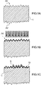
- a texturing of at least one face of the substrate 1 can be provided. This operation makes it possible to form a relief on the surface, for example in the form of micrometric pyramidal patterns.
- the texturing is typically carried out by mechanical action or by chemical attack, for example by placing the substrate 1 in a bath containing a KOH solution.
- a texturing of the substrate 1 is implemented both at its front face AV and at its rear face AR.
- front face is meant in this example a main face of the substrate 1 which is intended to be directly exposed to the sun, while the “rear face” is the main face opposite the front face.
- the figure 1B illustrates a subsequent step of doping an area of substrate 1 which extends along a first of its main faces AV, AR.
- the doping of the first face or front face AV is typically carried out by implantation.
- Such a layout is preferably uniform on the front front face.
- the doping is carried out by implantation by plasma immersion (PIII for “Plasma Immersion Ion Implantation”).
- PIII Plasma immersion Ion Implantation
- This technique which uses a plasma as a source of species, makes it possible to carry out an implantation at reduced cost.
- This type of so-called “multi-energetic” implantation leads to a maximum dopant concentration profile at the surface. It thus makes it possible to obtain a very high concentration of dopants at the level of the surface after implantation, thus being able to increase the phenomenon of desorption of phosphorus.
- the concentrations of dopants at the level of the surface after implantation are greater than 1 ⁇ 10 20 at/cm 3 .
- the N-type doping of the first face is carried out by means of phosphorus.
- the implantation can be carried out in the presence of a gaseous precursor of the phosphine PH 3 type.
- the implantation can in particular be provided with a dose for example comprised between 5 ⁇ 10 14 at/cm 2 and 2 ⁇ 10 16 at/cm 2 and an acceleration voltage comprised for example between 100 V and 10 kV.
- the dose is given here in the case of a PIII implantation from PH 3 gas, the latter comprising both the plasma ions containing phosphorus and the hydrogen ions.
- implanted phosphorus can desorb and react with surrounding oxygen to form a layer of phosphorus oxide.
- this phosphorus desorption phenomenon is avoided or limited at the level of at least one given localized region of the first AV face.
- a localized barrier layer is formed on this given region.
- a waiting time is preferably provided, between the end of the implantation step and the production of this barrier layer, as short as possible.
- this waiting time is less than 24 hours and preferably less than 1 hour.
- the figure 1C illustrates a step of forming the barrier layer 5 on a region 11 of the first face AV doped by implantation and to which provision is made to confer a high concentration of dopants, in particular according to an N++ doping.
- N++ doping or “high” concentration of dopants we mean here a maximum concentration of active dopants typically greater than 1 ⁇ 10 19 at/cm 3 typically between 1 ⁇ 10 20 at/cm 3 and 5 ⁇ 10 20 at/cm 3 .
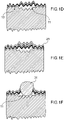
- the barrier layer 5 is thus arranged on a region 11 of the face AV of the substrate 1 at the level of which it is desired to avoid or at least limit a phenomenon of desorption of dopants. At least one other region 13 of the face AV adjacent to region 11 is revealed and is not covered by this barrier layer 5. At this other region 13, the desorption of phosphorus is therefore not slowed down or blocked.
- the barrier layer 5 can be formed by depositing a material through one or more opening(s) of a mask affixed or formed on the front face AV.
- the mask (not shown) may for example be made of graphite, or of silicon, or of a ceramic material, or of a metallic material.
- barrier layer 5 is a full plate deposit of material, that is to say covering the entire front face AV.
- one or more patterns are then formed in the full plate deposited layer.
- the pattern(s) can be formed by direct writing, without using a mask, for example by using a laser or a lithography technique.
- the barrier layer 5 can be made of one material or a stack of several materials.
- the barrier layer 5 can be based on silicon oxide (SiO x ), or silicon nitride (SiN), or silicon nitride incorporating oxygen, or silicon oxynitride.
- SiO x silicon oxide
- SiN silicon nitride
- silicon nitride incorporating oxygen, or silicon oxynitride it consists of a dielectric material or a stack of dielectric materials, such as silicon oxide, silicon nitride or silicon oxynitride.
- a barrier layer 5 of dielectric material is provided so that certain zones of the latter can be used subsequently for passivation.
- the barrier layer 5 typically has a thickness comprised between 5 nm and 150 nm.
- the barrier layer 5 is preferably provided in a material and a thickness so as to block or slow down the diffusion of phosphorus. Those skilled in the art specializing in implantations will know how to choose the material and the thickness of the barrier layer so as to block or slow down the diffusion of the atoms.
- the barrier layer 5 is a layer of silicon nitride SiN x having a thickness which can be between 5 nm and 150 nm, preferably between 10 and 100 nm and, for example, of the order of 70 nm.
- the deposition of the barrier layer 5 is carried out by a PECVD technique (for “Plasma-Enhanced Chemical Vapor Deposition”, in French “plasma-assisted chemical vapor deposition”).
- the barrier layer 5 is planned to carry out the deposition of the barrier layer 5 at low temperature, in particular in order to avoid a modification of the surface state of the region 13 opposite which it is not desired to preserve or produce the barrier layer 5 and thus avoid limiting the phenomenon of desorption in this zone.
- a deposition temperature of less than 450° C. and preferably less than 300° C. and preferably between 150° C. and 250° C. is typically chosen.
- the barrier layer 5 when it is made of silicon nitride can be deposited at a temperature of the order of 200° C. in order to be able to produce regions 11, 13 doped with different profiles and/or concentrations, in particular N+ and N++, having significant deviations in terms of sheet resistance and this, over a very wide range of activation annealing conditions.
- the uncovered region 13 is a portion that we wishes to boost N+.
- N+ doping is meant here a maximum concentration of active dopants typically less than 4 ⁇ 10 20 at/cm 3 typically between 8 ⁇ 10 19 at/cm 3 and 3 ⁇ 10 20 at/cm 3 .
- the activation annealing can be carried out at a temperature comprised for example between 780° C. and 1100° C. and according to a planned duration, for example between 1 s min and 120 min.
- annealing profiles can be implemented.
- Another exemplary embodiment provides for the use of “spike” type annealing, in other words with a temperature profile in the form of a peak, that is to say with a rapid rise in temperature, for example of the order of a few seconds while immediately followed by a rapid drop in temperature of the order of a few seconds.
- activation annealing conditions in particular in terms of temperature and duration depending on the temperature at which the barrier layer 5 has been deposited and depending on the dopant concentration profile desired for the areas N+ and N++ doped.
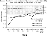
- the curves C0, C1, C2 are all representative of a difference in square resistance at the end of the activation annealing, between a region 11 covered by a barrier layer 5 of nitride and another region 13 not covered by this barrier layer 5 as a function of different activation annealing conditions for a given PIII implantation condition from the precursor gas PH3.
- the curves C0, C1, C2 represent a resistance difference variation respectively for, a barrier layer deposition temperature of 200°C, a barrier layer deposition temperature of 300°C, a deposition temperature of 450°C. It is thus found that below a certain deposition temperature of the barrier layer, it is possible, for very variable activation annealing conditions, to obtain a sufficient square resistance difference, that is to say typically higher at 5 ⁇ /square.
- a heavily doped region 11 is obtained under the barrier layer 5, for example an N++ doped region with a dopant concentration which can be between 1 ⁇ 10 20 at/cm 3 and 5 ⁇ 10 20 at/cm 3 , and another region 13 less doped than the given region 11, in particular N+ doped.
- Region 13 which is more weakly doped can have a dopant concentration of between 8 ⁇ 10 19 at/cm 3 and 3 ⁇ 10 20 at/cm 3 .
- the different doping profiles obtained at the end of the activation annealing between on the one hand the masked region 11 and on the other hand the other non-masked region(s) 13 can be measured by a technique electrochemical capacitance-voltage profiling ECV (acronym for “Electrochemical Capacitance-Voltage”) making it possible to obtain a concentration profile of active carriers in the semiconductor layer of the substrate 1, or alternatively by a technique of the SIMS type (for “ Secondary Ion Mass Spectrometry”).
- ECV electrochemical capacitance-voltage profiling
- SIMS type for “ Secondary Ion Mass Spectrometry”.
- the respective doping levels are also quantifiable by means of a 4-point type electrical measurement.
- the region 11 covered by the barrier layer 5 and which has a more substantial doping can be provided to make contact.
- a layer 25 based on a material, preferably dielectric, and of a thickness provided so as to serve as anti-reflection.
- the antireflection layer 25, for example in SiNx, makes it possible to reduce the optical losses linked to the reflections of the light radiation and to optimize the absorption of the light radiation by the substrate 1.
- an antireflection layer 25 in SiN x can also be used as a layer dedicated to passivation.
- At least one metallic electrode 31 is formed on the first face AV, and in particular in contact with the N++-doped region 11.
- this step includes a metallization which can be carried out by screen printing.
- the electrode 31 can be formed from a layer of transparent conductive oxide such as ITO on which rests a metallic layer, for example based on Ag.
- the electrode 31 can be formed by the deposition by screen printing of a metal paste, for example based on silver, followed by annealing of the contact.
- the metal deposit and the region 11 on which it is produced can take the form of a grid.
- the annealing of the contact can be done for example in an oven with an infrared lamp and can allow the silver-based paste to pass through the antireflection layer 25 and the barrier layer 5 if the latter is retained.
- the electrode 31 can be made, by making an opening through the antireflection layer 25 and the barrier layer 5 in the case where the latter has been retained, through which at least one deposit of metallic material is made.
- the barrier layer 5 When the barrier layer 5 is made of an electrically insulating material, it can form a passivation.
- Such a method can however also be used in order to produce zones of different dopings and/or profiles, in particular adjacent zones N++ and N+ in another type of device, and for example in a microelectronic or optoelectronic device.
Landscapes
- Photovoltaic Devices (AREA)
Claims (9)
- Verfahren zur Herstellung einer Halbleiterstruktur für Solarzelle mit N-dotierten Bereichen, die unterschiedliche Dotierungsprofile und/oder - konzentrationen haben, umfassend die folgenden Schritte:- Implantieren einer dotierenden Spezies, insbesondere von Phosphor, in einen Oberflächenbereich eines Halbleitersubstrats (1),- dann Bilden einer Sperrschicht (5) auf mindestens einer ersten Region (11) des Oberflächenbereichs, wohingegen mindestens eine zweite Region (13) des Oberflächenbereichs, die zu der ersten Region benachbart ist, frei ist und nicht von der Sperrschicht bedeckt ist,- Durchführen mindestens eines Aktivierungstemperns von Dotierungsmitteln des Oberflächenbereichs, so dass eine N-Dotierung dieses Oberflächenbereichs durchgeführt wird, wohingegen die Sperrschicht (5) auf der ersten Region (11) beibehalten wird und die zweite Region frei ist und nicht von der Sperrschicht bedeckt ist, was zu einer Desorption der dotierenden Spezies im Bereich der zweiten Region (13) führt, wobei die auf der ersten Region (11) beibehaltene Sperrschicht eine Desorption der dotierenden Spezies im Bereich der ersten Region (11) verhindert oder begrenzt.
- Verfahren nach Anspruch 1, wobei die Sperrschicht (5) auf der Basis eines dielektrischen Materials ist; insbesondere auf der Basis von Siliciumnitrid oder von Siliciumoxid oder von Siliciumoxinitrid.
- Verfahren nach Anspruch 2, wobei die Sperrschicht eine Dicke hat, die zwischen 5 nm und 150 nm liegt.
- Verfahren nach einem der Ansprüche 1 bis 3, wobei die Sperrschicht bei einer Temperatur von unter 450 °C, vorzugsweise von unter 300 °C, aufgebracht wird.
- Verfahren nach einem der Ansprüche 1 bis 4, wobei sich der Oberflächenbereich gegen und in einer texturierten Fläche (AV) des Substrats (1) erstreckt, die mit Reliefmotiven dotiert ist.
- Verfahren nach einem der Ansprüche 1 bis 5, wobei die Implantierung durch Plasmaimmersion (PIII) durchgeführt wird.
- Verfahren nach einem der Ansprüche 1 bis 6, wobei nach Abschluss des mindestens einen Aktivierungstemperns die ersten Region N+-dotiert ist, die zweite Region N++-dotiert ist.
- Verfahren nach einem der Ansprüche 1 bis 7, wobei nach Abschluss des mindestens einen Aktivierungstemperns der Unterschied zwischen dem Quadratwiderstand der ersten Region und dem Quadratwiderstand der zweiten Region mindestens 5 Ohm/Quadrat beträgt.
- Verfahren zur Herstellung einer Solarzelle, umfassend:- das Herstellen einer Struktur nach einem Verfahren nach einem der Ansprüche 1 bis 8, dann- das Bilden eines Kontakts (31) auf der ersten Region (11).
Applications Claiming Priority (2)
| Application Number | Priority Date | Filing Date | Title |
|---|---|---|---|
| FR1859498A FR3087296B1 (fr) | 2018-10-12 | 2018-10-12 | Realisation de zones dopees n+ et n++ pour cellule solaire |
| PCT/FR2019/052390 WO2020074824A1 (fr) | 2018-10-12 | 2019-10-09 | Realisation de zones dopees n+ et n++ pour cellule solaire |
Publications (2)
| Publication Number | Publication Date |
|---|---|
| EP3841618A1 EP3841618A1 (de) | 2021-06-30 |
| EP3841618B1 true EP3841618B1 (de) | 2022-08-24 |
Family
ID=65951642
Family Applications (1)
| Application Number | Title | Priority Date | Filing Date |
|---|---|---|---|
| EP19823793.5A Active EP3841618B1 (de) | 2018-10-12 | 2019-10-09 | Erzeugung von n+- und n++-dotierten bereichen für eine solarzelle |
Country Status (3)
| Country | Link |
|---|---|
| EP (1) | EP3841618B1 (de) |
| FR (1) | FR3087296B1 (de) |
| WO (1) | WO2020074824A1 (de) |
Family Cites Families (3)
| Publication number | Priority date | Publication date | Assignee | Title |
|---|---|---|---|---|
| US4283031A (en) | 1977-12-14 | 1981-08-11 | Finch Colin M | System controlling apparatus which compares signals from sensors monitoring passing objects with pre-determined parameter information to control the system |
| US20090142875A1 (en) * | 2007-11-30 | 2009-06-04 | Applied Materials, Inc. | Method of making an improved selective emitter for silicon solar cells |
| KR101902887B1 (ko) | 2011-12-23 | 2018-10-01 | 엘지전자 주식회사 | 태양 전지의 제조 방법 |
-
2018
- 2018-10-12 FR FR1859498A patent/FR3087296B1/fr not_active Expired - Fee Related
-
2019
- 2019-10-09 EP EP19823793.5A patent/EP3841618B1/de active Active
- 2019-10-09 WO PCT/FR2019/052390 patent/WO2020074824A1/fr not_active Ceased
Also Published As
| Publication number | Publication date |
|---|---|
| FR3087296B1 (fr) | 2022-01-14 |
| WO2020074824A1 (fr) | 2020-04-16 |
| EP3841618A1 (de) | 2021-06-30 |
| FR3087296A1 (fr) | 2020-04-17 |
Similar Documents
| Publication | Publication Date | Title |
|---|---|---|
| US12532571B2 (en) | Back contact solar cell and fabrication method thereof | |
| FR2988908A1 (fr) | Procede de fabrication d'une cellule photovoltaique a contacts interdigites en face arriere | |
| CN110943143A (zh) | 用于制造具有异质结和发射极扩散区的光伏太阳能电池的方法 | |
| EP2965350A1 (de) | Monolithisches halbleitersubstrat auf der basis von silicium, in unterzellen unterteilt | |
| FR3058264A1 (fr) | Procede de fabrication de cellules photovoltaiques a contacts arriere. | |
| FR3071358B1 (fr) | Procede de fabrication d'une cellule photovoltaique a homojonction | |
| EP3841618B1 (de) | Erzeugung von n+- und n++-dotierten bereichen für eine solarzelle | |
| EP3347921A1 (de) | Verfahren zur herstellung einer elektronischen verbindungsvorrichtung und zugehörige vorrichtung | |
| EP3660928B1 (de) | Herstellungsverfahren von fotovoltaik-solarzellen | |
| EP3673518B1 (de) | Verbessertes verfahren zur dotierung von solarzellen | |
| EP2801118B1 (de) | Herstellungsverfahren für fotovoltaische zellen | |
| EP4117045B1 (de) | Verfahren zur herstellung einer tandem-fotovoltaikzelle | |
| EP3242335B1 (de) | Verfahren zur herstellung einer fotovoltaischen zelle mit einem heteroübergang | |
| FR3048819A1 (fr) | Compensation de dopage par irradiation laser pour la fabrication de cellules solaires a heterojonction | |
| FR3003089A1 (fr) | Plaquette de silicium monolithique a multi-jonctions p/n verticales. | |
| EP3213352B1 (de) | Verfahren zur herstellung einer fotovoltaikzelle | |
| US7994064B2 (en) | Selective etch for damage at exfoliated surface | |
| EP4113634A1 (de) | Verfahren zur herstellung einer fotovoltaikzelle mit passiven kontakten | |
| EP4336569A1 (de) | Photovoltaische zelle mit doppelseitenigen passivkontakten und mit unter den vorderen metallisierungen lokalisierten tco-teilen | |
| EP3826077A1 (de) | Verfahren zur herstellung einer fotovoltaikzelle | |
| FR3103058A1 (fr) | Procédé de réalisation d’une jonction tunnel d’une cellule photovoltaïque |
Legal Events
| Date | Code | Title | Description |
|---|---|---|---|
| STAA | Information on the status of an ep patent application or granted ep patent |
Free format text: STATUS: UNKNOWN |
|
| STAA | Information on the status of an ep patent application or granted ep patent |
Free format text: STATUS: THE INTERNATIONAL PUBLICATION HAS BEEN MADE |
|
| PUAI | Public reference made under article 153(3) epc to a published international application that has entered the european phase |
Free format text: ORIGINAL CODE: 0009012 |
|
| STAA | Information on the status of an ep patent application or granted ep patent |
Free format text: STATUS: REQUEST FOR EXAMINATION WAS MADE |
|
| 17P | Request for examination filed |
Effective date: 20210325 |
|
| AK | Designated contracting states |
Kind code of ref document: A1 Designated state(s): AL AT BE BG CH CY CZ DE DK EE ES FI FR GB GR HR HU IE IS IT LI LT LU LV MC MK MT NL NO PL PT RO RS SE SI SK SM TR |
|
| DAV | Request for validation of the european patent (deleted) | ||
| DAX | Request for extension of the european patent (deleted) | ||
| GRAP | Despatch of communication of intention to grant a patent |
Free format text: ORIGINAL CODE: EPIDOSNIGR1 |
|
| STAA | Information on the status of an ep patent application or granted ep patent |
Free format text: STATUS: GRANT OF PATENT IS INTENDED |
|
| INTG | Intention to grant announced |
Effective date: 20220321 |
|
| GRAS | Grant fee paid |
Free format text: ORIGINAL CODE: EPIDOSNIGR3 |
|
| GRAA | (expected) grant |
Free format text: ORIGINAL CODE: 0009210 |
|
| STAA | Information on the status of an ep patent application or granted ep patent |
Free format text: STATUS: THE PATENT HAS BEEN GRANTED |
|
| AK | Designated contracting states |
Kind code of ref document: B1 Designated state(s): AL AT BE BG CH CY CZ DE DK EE ES FI FR GB GR HR HU IE IS IT LI LT LU LV MC MK MT NL NO PL PT RO RS SE SI SK SM TR |
|
| REG | Reference to a national code |
Ref country code: CH Ref legal event code: EP |
|
| REG | Reference to a national code |
Ref country code: IE Ref legal event code: FG4D Free format text: LANGUAGE OF EP DOCUMENT: FRENCH |
|
| REG | Reference to a national code |
Ref country code: AT Ref legal event code: REF Ref document number: 1514262 Country of ref document: AT Kind code of ref document: T Effective date: 20220915 Ref country code: DE Ref legal event code: R096 Ref document number: 602019018774 Country of ref document: DE |
|
| REG | Reference to a national code |
Ref country code: LT Ref legal event code: MG9D |
|
| REG | Reference to a national code |
Ref country code: NL Ref legal event code: MP Effective date: 20220824 |
|
| PG25 | Lapsed in a contracting state [announced via postgrant information from national office to epo] |
Ref country code: SE Free format text: LAPSE BECAUSE OF FAILURE TO SUBMIT A TRANSLATION OF THE DESCRIPTION OR TO PAY THE FEE WITHIN THE PRESCRIBED TIME-LIMIT Effective date: 20220824 Ref country code: RS Free format text: LAPSE BECAUSE OF FAILURE TO SUBMIT A TRANSLATION OF THE DESCRIPTION OR TO PAY THE FEE WITHIN THE PRESCRIBED TIME-LIMIT Effective date: 20220824 Ref country code: PT Free format text: LAPSE BECAUSE OF FAILURE TO SUBMIT A TRANSLATION OF THE DESCRIPTION OR TO PAY THE FEE WITHIN THE PRESCRIBED TIME-LIMIT Effective date: 20221226 Ref country code: NO Free format text: LAPSE BECAUSE OF FAILURE TO SUBMIT A TRANSLATION OF THE DESCRIPTION OR TO PAY THE FEE WITHIN THE PRESCRIBED TIME-LIMIT Effective date: 20221124 Ref country code: NL Free format text: LAPSE BECAUSE OF FAILURE TO SUBMIT A TRANSLATION OF THE DESCRIPTION OR TO PAY THE FEE WITHIN THE PRESCRIBED TIME-LIMIT Effective date: 20220824 Ref country code: LV Free format text: LAPSE BECAUSE OF FAILURE TO SUBMIT A TRANSLATION OF THE DESCRIPTION OR TO PAY THE FEE WITHIN THE PRESCRIBED TIME-LIMIT Effective date: 20220824 Ref country code: LT Free format text: LAPSE BECAUSE OF FAILURE TO SUBMIT A TRANSLATION OF THE DESCRIPTION OR TO PAY THE FEE WITHIN THE PRESCRIBED TIME-LIMIT Effective date: 20220824 Ref country code: FI Free format text: LAPSE BECAUSE OF FAILURE TO SUBMIT A TRANSLATION OF THE DESCRIPTION OR TO PAY THE FEE WITHIN THE PRESCRIBED TIME-LIMIT Effective date: 20220824 |
|
| REG | Reference to a national code |
Ref country code: AT Ref legal event code: MK05 Ref document number: 1514262 Country of ref document: AT Kind code of ref document: T Effective date: 20220824 |
|
| PG25 | Lapsed in a contracting state [announced via postgrant information from national office to epo] |
Ref country code: PL Free format text: LAPSE BECAUSE OF FAILURE TO SUBMIT A TRANSLATION OF THE DESCRIPTION OR TO PAY THE FEE WITHIN THE PRESCRIBED TIME-LIMIT Effective date: 20220824 Ref country code: IS Free format text: LAPSE BECAUSE OF FAILURE TO SUBMIT A TRANSLATION OF THE DESCRIPTION OR TO PAY THE FEE WITHIN THE PRESCRIBED TIME-LIMIT Effective date: 20221224 Ref country code: HR Free format text: LAPSE BECAUSE OF FAILURE TO SUBMIT A TRANSLATION OF THE DESCRIPTION OR TO PAY THE FEE WITHIN THE PRESCRIBED TIME-LIMIT Effective date: 20220824 Ref country code: GR Free format text: LAPSE BECAUSE OF FAILURE TO SUBMIT A TRANSLATION OF THE DESCRIPTION OR TO PAY THE FEE WITHIN THE PRESCRIBED TIME-LIMIT Effective date: 20221125 |
|
| PG25 | Lapsed in a contracting state [announced via postgrant information from national office to epo] |
Ref country code: SM Free format text: LAPSE BECAUSE OF FAILURE TO SUBMIT A TRANSLATION OF THE DESCRIPTION OR TO PAY THE FEE WITHIN THE PRESCRIBED TIME-LIMIT Effective date: 20220824 Ref country code: RO Free format text: LAPSE BECAUSE OF FAILURE TO SUBMIT A TRANSLATION OF THE DESCRIPTION OR TO PAY THE FEE WITHIN THE PRESCRIBED TIME-LIMIT Effective date: 20220824 Ref country code: ES Free format text: LAPSE BECAUSE OF FAILURE TO SUBMIT A TRANSLATION OF THE DESCRIPTION OR TO PAY THE FEE WITHIN THE PRESCRIBED TIME-LIMIT Effective date: 20220824 Ref country code: DK Free format text: LAPSE BECAUSE OF FAILURE TO SUBMIT A TRANSLATION OF THE DESCRIPTION OR TO PAY THE FEE WITHIN THE PRESCRIBED TIME-LIMIT Effective date: 20220824 Ref country code: CZ Free format text: LAPSE BECAUSE OF FAILURE TO SUBMIT A TRANSLATION OF THE DESCRIPTION OR TO PAY THE FEE WITHIN THE PRESCRIBED TIME-LIMIT Effective date: 20220824 Ref country code: AT Free format text: LAPSE BECAUSE OF FAILURE TO SUBMIT A TRANSLATION OF THE DESCRIPTION OR TO PAY THE FEE WITHIN THE PRESCRIBED TIME-LIMIT Effective date: 20220824 |
|
| REG | Reference to a national code |
Ref country code: DE Ref legal event code: R097 Ref document number: 602019018774 Country of ref document: DE |
|
| PG25 | Lapsed in a contracting state [announced via postgrant information from national office to epo] |
Ref country code: SK Free format text: LAPSE BECAUSE OF FAILURE TO SUBMIT A TRANSLATION OF THE DESCRIPTION OR TO PAY THE FEE WITHIN THE PRESCRIBED TIME-LIMIT Effective date: 20220824 Ref country code: MC Free format text: LAPSE BECAUSE OF FAILURE TO SUBMIT A TRANSLATION OF THE DESCRIPTION OR TO PAY THE FEE WITHIN THE PRESCRIBED TIME-LIMIT Effective date: 20220824 Ref country code: EE Free format text: LAPSE BECAUSE OF FAILURE TO SUBMIT A TRANSLATION OF THE DESCRIPTION OR TO PAY THE FEE WITHIN THE PRESCRIBED TIME-LIMIT Effective date: 20220824 |
|
| REG | Reference to a national code |
Ref country code: CH Ref legal event code: PL |
|
| REG | Reference to a national code |
Ref country code: BE Ref legal event code: MM Effective date: 20221031 |
|
| PG25 | Lapsed in a contracting state [announced via postgrant information from national office to epo] |
Ref country code: LU Free format text: LAPSE BECAUSE OF NON-PAYMENT OF DUE FEES Effective date: 20221009 Ref country code: AL Free format text: LAPSE BECAUSE OF FAILURE TO SUBMIT A TRANSLATION OF THE DESCRIPTION OR TO PAY THE FEE WITHIN THE PRESCRIBED TIME-LIMIT Effective date: 20220824 |
|
| PLBE | No opposition filed within time limit |
Free format text: ORIGINAL CODE: 0009261 |
|
| STAA | Information on the status of an ep patent application or granted ep patent |
Free format text: STATUS: NO OPPOSITION FILED WITHIN TIME LIMIT |
|
| PG25 | Lapsed in a contracting state [announced via postgrant information from national office to epo] |
Ref country code: LI Free format text: LAPSE BECAUSE OF NON-PAYMENT OF DUE FEES Effective date: 20221031 Ref country code: CH Free format text: LAPSE BECAUSE OF NON-PAYMENT OF DUE FEES Effective date: 20221031 |
|
| 26N | No opposition filed |
Effective date: 20230525 |
|
| PG25 | Lapsed in a contracting state [announced via postgrant information from national office to epo] |
Ref country code: SI Free format text: LAPSE BECAUSE OF FAILURE TO SUBMIT A TRANSLATION OF THE DESCRIPTION OR TO PAY THE FEE WITHIN THE PRESCRIBED TIME-LIMIT Effective date: 20220824 |
|
| PG25 | Lapsed in a contracting state [announced via postgrant information from national office to epo] |
Ref country code: BE Free format text: LAPSE BECAUSE OF NON-PAYMENT OF DUE FEES Effective date: 20221031 |
|
| PG25 | Lapsed in a contracting state [announced via postgrant information from national office to epo] |
Ref country code: IE Free format text: LAPSE BECAUSE OF NON-PAYMENT OF DUE FEES Effective date: 20221009 |
|
| PG25 | Lapsed in a contracting state [announced via postgrant information from national office to epo] |
Ref country code: CY Free format text: LAPSE BECAUSE OF FAILURE TO SUBMIT A TRANSLATION OF THE DESCRIPTION OR TO PAY THE FEE WITHIN THE PRESCRIBED TIME-LIMIT Effective date: 20220824 |
|
| PG25 | Lapsed in a contracting state [announced via postgrant information from national office to epo] |
Ref country code: MK Free format text: LAPSE BECAUSE OF FAILURE TO SUBMIT A TRANSLATION OF THE DESCRIPTION OR TO PAY THE FEE WITHIN THE PRESCRIBED TIME-LIMIT Effective date: 20220824 Ref country code: IT Free format text: LAPSE BECAUSE OF FAILURE TO SUBMIT A TRANSLATION OF THE DESCRIPTION OR TO PAY THE FEE WITHIN THE PRESCRIBED TIME-LIMIT Effective date: 20220824 Ref country code: HU Free format text: LAPSE BECAUSE OF FAILURE TO SUBMIT A TRANSLATION OF THE DESCRIPTION OR TO PAY THE FEE WITHIN THE PRESCRIBED TIME-LIMIT; INVALID AB INITIO Effective date: 20191009 |
|
| GBPC | Gb: european patent ceased through non-payment of renewal fee |
Effective date: 20231009 |
|
| PG25 | Lapsed in a contracting state [announced via postgrant information from national office to epo] |
Ref country code: GB Free format text: LAPSE BECAUSE OF NON-PAYMENT OF DUE FEES Effective date: 20231009 |
|
| PG25 | Lapsed in a contracting state [announced via postgrant information from national office to epo] |
Ref country code: GB Free format text: LAPSE BECAUSE OF NON-PAYMENT OF DUE FEES Effective date: 20231009 Ref country code: BG Free format text: LAPSE BECAUSE OF FAILURE TO SUBMIT A TRANSLATION OF THE DESCRIPTION OR TO PAY THE FEE WITHIN THE PRESCRIBED TIME-LIMIT Effective date: 20220824 |
|
| PG25 | Lapsed in a contracting state [announced via postgrant information from national office to epo] |
Ref country code: MT Free format text: LAPSE BECAUSE OF FAILURE TO SUBMIT A TRANSLATION OF THE DESCRIPTION OR TO PAY THE FEE WITHIN THE PRESCRIBED TIME-LIMIT Effective date: 20220824 |
|
| REG | Reference to a national code |
Ref country code: DE Ref legal event code: R079 Ref document number: 602019018774 Country of ref document: DE Free format text: PREVIOUS MAIN CLASS: H01L0031180000 Ipc: H10F0071000000 |
|
| PGFP | Annual fee paid to national office [announced via postgrant information from national office to epo] |
Ref country code: DE Payment date: 20241022 Year of fee payment: 6 |
|
| PGFP | Annual fee paid to national office [announced via postgrant information from national office to epo] |
Ref country code: FR Payment date: 20241024 Year of fee payment: 6 |
|
| PG25 | Lapsed in a contracting state [announced via postgrant information from national office to epo] |
Ref country code: TR Free format text: LAPSE BECAUSE OF FAILURE TO SUBMIT A TRANSLATION OF THE DESCRIPTION OR TO PAY THE FEE WITHIN THE PRESCRIBED TIME-LIMIT Effective date: 20220824 |