EP3673518B1 - Verbessertes verfahren zur dotierung von solarzellen - Google Patents
Verbessertes verfahren zur dotierung von solarzellen Download PDFInfo
- Publication number
- EP3673518B1 EP3673518B1 EP18827177.9A EP18827177A EP3673518B1 EP 3673518 B1 EP3673518 B1 EP 3673518B1 EP 18827177 A EP18827177 A EP 18827177A EP 3673518 B1 EP3673518 B1 EP 3673518B1
- Authority
- EP
- European Patent Office
- Prior art keywords
- doping
- substrate
- face
- type
- barrier layer
- Prior art date
- Legal status (The legal status is an assumption and is not a legal conclusion. Google has not performed a legal analysis and makes no representation as to the accuracy of the status listed.)
- Active
Links
Images


Classifications
-
- H—ELECTRICITY
- H10—SEMICONDUCTOR DEVICES; ELECTRIC SOLID-STATE DEVICES NOT OTHERWISE PROVIDED FOR
- H10F—INORGANIC SEMICONDUCTOR DEVICES SENSITIVE TO INFRARED RADIATION, LIGHT, ELECTROMAGNETIC RADIATION OF SHORTER WAVELENGTH OR CORPUSCULAR RADIATION
- H10F10/00—Individual photovoltaic cells, e.g. solar cells
- H10F10/10—Individual photovoltaic cells, e.g. solar cells having potential barriers
- H10F10/14—Photovoltaic cells having only PN homojunction potential barriers
-
- H—ELECTRICITY
- H10—SEMICONDUCTOR DEVICES; ELECTRIC SOLID-STATE DEVICES NOT OTHERWISE PROVIDED FOR
- H10F—INORGANIC SEMICONDUCTOR DEVICES SENSITIVE TO INFRARED RADIATION, LIGHT, ELECTROMAGNETIC RADIATION OF SHORTER WAVELENGTH OR CORPUSCULAR RADIATION
- H10F71/00—Manufacture or treatment of devices covered by this subclass
- H10F71/121—The active layers comprising only Group IV materials
-
- H—ELECTRICITY
- H10—SEMICONDUCTOR DEVICES; ELECTRIC SOLID-STATE DEVICES NOT OTHERWISE PROVIDED FOR
- H10P—GENERIC PROCESSES OR APPARATUS FOR THE MANUFACTURE OR TREATMENT OF DEVICES COVERED BY CLASS H10
- H10P30/00—Ion implantation into wafers, substrates or parts of devices
- H10P30/20—Ion implantation into wafers, substrates or parts of devices into semiconductor materials, e.g. for doping
- H10P30/202—Ion implantation into wafers, substrates or parts of devices into semiconductor materials, e.g. for doping characterised by the semiconductor materials
- H10P30/204—Ion implantation into wafers, substrates or parts of devices into semiconductor materials, e.g. for doping characterised by the semiconductor materials into Group IV semiconductors
-
- H—ELECTRICITY
- H10—SEMICONDUCTOR DEVICES; ELECTRIC SOLID-STATE DEVICES NOT OTHERWISE PROVIDED FOR
- H10P—GENERIC PROCESSES OR APPARATUS FOR THE MANUFACTURE OR TREATMENT OF DEVICES COVERED BY CLASS H10
- H10P30/00—Ion implantation into wafers, substrates or parts of devices
- H10P30/20—Ion implantation into wafers, substrates or parts of devices into semiconductor materials, e.g. for doping
- H10P30/21—Ion implantation into wafers, substrates or parts of devices into semiconductor materials, e.g. for doping of electrically active species
-
- H—ELECTRICITY
- H10—SEMICONDUCTOR DEVICES; ELECTRIC SOLID-STATE DEVICES NOT OTHERWISE PROVIDED FOR
- H10P—GENERIC PROCESSES OR APPARATUS FOR THE MANUFACTURE OR TREATMENT OF DEVICES COVERED BY CLASS H10
- H10P30/00—Ion implantation into wafers, substrates or parts of devices
- H10P30/20—Ion implantation into wafers, substrates or parts of devices into semiconductor materials, e.g. for doping
- H10P30/28—Ion implantation into wafers, substrates or parts of devices into semiconductor materials, e.g. for doping characterised by an annealing step, e.g. for activation of dopants
-
- Y—GENERAL TAGGING OF NEW TECHNOLOGICAL DEVELOPMENTS; GENERAL TAGGING OF CROSS-SECTIONAL TECHNOLOGIES SPANNING OVER SEVERAL SECTIONS OF THE IPC; TECHNICAL SUBJECTS COVERED BY FORMER USPC CROSS-REFERENCE ART COLLECTIONS [XRACs] AND DIGESTS
- Y02—TECHNOLOGIES OR APPLICATIONS FOR MITIGATION OR ADAPTATION AGAINST CLIMATE CHANGE
- Y02E—REDUCTION OF GREENHOUSE GAS [GHG] EMISSIONS, RELATED TO ENERGY GENERATION, TRANSMISSION OR DISTRIBUTION
- Y02E10/00—Energy generation through renewable energy sources
- Y02E10/50—Photovoltaic [PV] energy
- Y02E10/547—Monocrystalline silicon PV cells
-
- Y—GENERAL TAGGING OF NEW TECHNOLOGICAL DEVELOPMENTS; GENERAL TAGGING OF CROSS-SECTIONAL TECHNOLOGIES SPANNING OVER SEVERAL SECTIONS OF THE IPC; TECHNICAL SUBJECTS COVERED BY FORMER USPC CROSS-REFERENCE ART COLLECTIONS [XRACs] AND DIGESTS
- Y02—TECHNOLOGIES OR APPLICATIONS FOR MITIGATION OR ADAPTATION AGAINST CLIMATE CHANGE
- Y02P—CLIMATE CHANGE MITIGATION TECHNOLOGIES IN THE PRODUCTION OR PROCESSING OF GOODS
- Y02P70/00—Climate change mitigation technologies in the production process for final industrial or consumer products
- Y02P70/50—Manufacturing or production processes characterised by the final manufactured product
Definitions
- the quantity of dopants of the first type incorporated by means of the barrier layer in the semiconductor material is provided such that the doped zones at the level of the lateral edges of the substrate are generally doped according to the first type of doping, in particular. N + or N ++.
- the doping of the first type exceeds that of the second type (for example of type P).
- the barrier layer can advantageously be formed so as to cover peripheral regions of the rear face of the substrate.
- the lateral edges of the substrate and the periphery of the rear face of the substrate are thus advantageously protected.
- a particular embodiment provides a barrier layer doped with phosphorus in particular to perform an N-type doping, while the given doping species implanted on the front face is boron in order to perform a P-type doping at the front face.
- a particular embodiment provides for the implementation of a barrier layer based on silicon nitride doped with phosphorus (SiN: P) or silicon oxide doped with phosphorus (SiO: P).
- a texturing of at least one face of the substrate 1 is advantageously provided. This operation makes it possible to form a relief on the surface, for example in the form of micrometric pyramidal patterns.
- the texturing can be carried out by mechanical action or by chemical attack, for example by placing the substrate 1 in a bath containing a KOH solution.
- a texturing of the substrate 1 is implemented both at its front face AV and at its rear face AR.
- front face AV is meant in this example a face of the substrate 1 which is intended to be directly exposed to the sun, while the “rear face” AR is that opposite to the front face.
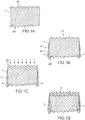
- the barrier layer 4 is provided in particular to protect the substrate 1 during a subsequent doping step by implantation, in particular of the front face AV. in order to carry out doping at the level of the edges 2 of the substrate 1, in particular a doping of the type opposite to that provided for the front face intended to be carried out subsequently.
- the barrier layer 4 is based on a dielectric material and can thus be adapted to carry out a passivation of the lateral edges of the substrate 1.
- this dielectric material can be silicon nitride doped with phosphorus (SiN: P), of oxide. of silicon doped with phosphorus (SiO: P) or one of their derivatives such as a silicon oxynitride doped with phosphorus.
- the barrier layer 4 is produced by vacuum deposition, for example using a PECVD technique (for “Plasma Enhanced Chemical Vapor Deposition”).
- the barrier layer 4 in addition to covering the lateral edges, is also produced so as to cover and protect peripheral zones 3a of the rear face AR of the substrate 1.
- a thermal annealing is carried out at a temperature and according to a suitable duration so as to activate the dopants of the doped region 6 situated at the level of the front face AV.
- Annealing is also provided to make it possible to diffuse the dopants contained in the barrier layer 4.
- the annealing can be carried out at a temperature of for example between 800 ° C and 1100 ° C, according to a duration which can be for example between 1 minute and 90 minutes.
- the zones 9 formed can, for example, be N + or N ++ doped.
- doping of a region 10 which extends along the rear face AR of the substrate 1 is implemented in order to produce a doped region 10 commonly called BSF (“Back Surface Field”).
- BSF Back Surface Field
- an N-type doping is carried out, this region 10 thus having a conductivity of the same type as that of the starting substrate 1.
- the doping of the rear face AR is in this case typically carried out using phosphorus.
- This doping can be carried out by implantation ( figure 1E ).
- a conventional ion implantation is used, that is to say using a directional beam or else an implantation by plasma immersion. It is also possible to envisage carrying out such doping by diffusion.
- thermal oxidation can be carried out once the activation annealing has been carried out.
- a layer 15 based on a material, preferably dielectric, and of thickness provided so as to serve as an anti-reflection.
- a material preferably dielectric, and of thickness provided so as to serve as an anti-reflection.
- the anti-reflection layer 15 for example made of SiNx, makes it possible to reduce the optical losses linked to the reflections of the light radiation and to optimize the absorption of the light radiation from the substrate 1.
- an antireflection layer 15 made of SiNx can also be used as a layer dedicated to passivation.
- metal electrodes 21 are formed on the front face AV and on the rear face AR of the substrate. Typically, this step comprises a metallization which can be carried out by screen printing.
- the electrodes 21 can be formed of a transparent conductive oxide layer such as ITO on which a metallic layer, for example based on Ag, rests.
- the barrier layer 4 can be retained at the end of the process.
- the barrier layer thus not only makes it possible to compensate for the effects of doping by implantation of boron ions on the front face but also to form a passivation of the slices or lateral edges of the substrate.
- a common dopant activation annealing for the front face and the rear face.
- doping is carried out by implantation of the front face then of the rear face, or else doping by implantation of the rear face then of the front face. Then, once these dopings have been carried out, a common activation annealing is carried out.
- the table below gives comparative results of measurements of certain performance factors between a batch of solar cells provided with a barrier layer and implemented using a method as described above, and a reference batch. .
- the performance factors evaluated are the PFF ("Pseudo Field-Factor"), the parallel resistance Rshunt (the value of which is inverse is representative of edge leakage currents) and the saturation current density J02 of a diode when considering an electrical circuit equivalent to a solar cell with a diode and a shunt resistor.
- PFF Pulseudo Field-Factor
- Rshunt the saturation current density J02 of a diode when considering an electrical circuit equivalent to a solar cell with a diode and a shunt resistor.
Landscapes
- Photovoltaic Devices (AREA)
Claims (9)
- Verfahren zum Herstellen einer photovoltaischen Zelle, das die folgenden Schritte umfasst:- Bilden einer Sperrschicht (4), die mindestens einen Dotierstoff enthält, auf Bereichen (2a) von Seitenkanten (2) eines Substrats (1) auf Basis von Halbleitermaterial, wobei die Sperrschicht (4) auf Basis eines dielektrischen Materials besteht, wobei der Dotierstoff geeignet ist, eine Dotierung eines ersten Typs, insbesondere eine n-Dotierung, des Halbleitermaterials durchzuführen, wobei sich die Seitenkanten (2) des Substrats zwischen einer ersten Seite (AV) und einer der ersten Seite entgegengesetzten zweiten Seite (AR) des Substrats erstrecken,- Implantation in die erste Seite (AV) des Substrats (1) von zumindest einer gegebenen Dotierstoffspezies, die geeignet ist, eine Dotierung eines zweiten Typs, insbesondere eine p-Dotierung, entgegengesetzt zum ersten Dotierungstyp durchzuführen, wobei die Sperrschicht (4) dazu ausgelegt ist, ein Eindringen der Dotierstoffspezies in den Bereich der Seitenkanten des Substrats zu begrenzen,- thermisches Tempern, um eine Diffusion des in der Sperrschicht (4) enthaltenen Dotierstoffs in das Halbleitermaterial an den Seitenkanten des Substrats zu erreichen, so dass die bei der Implantation erhaltene Dotierung in der ersten Seite (AV) des Substrats (1) kompensiert oder überschritten wird.
- Verfahren nach Anspruch 1, wobei die Sperrschicht (4) so gebildet wird, dass sie Umfangsbereiche (3a) der zweiten Seite (AR) des Substrats (1) bedeckt.
- Verfahren nach Anspruch 2, wobei die Sperrschicht (4) durch lokalisierte Abscheidung gebildet wird, während eine Maskierung auf der zweiten Seite (AR) des Substrats angeordnet ist, wobei die Umfangsbereiche (3a) der zweiten Seite (AR) nicht von der Maskierung bedeckt sind.
- Verfahren nach einem der Ansprüche 1 bis 3, wobei die Implantation in die erste Seite (AV) des Substrats (1) durch Plasmatauchen erfolgt.
- Verfahren nach einem der Ansprüche 1 bis 4, wobei das thermische Tempern mit einer Zeit und Temperatur erfolgt, die so angepasst sind, dass zugleich eine Aktivierung der gegebenen Dotierstoffspezies durchgeführt wird, die im Bereich der ersten Seite (AV) des Substrats implantiert ist.
- Verfahren nach einem der Ansprüche 1 bis 5, ferner umfassend die folgenden Schritte:- Dotierung eines ersten Typs, insbesondere n-Dotierung, im Bereich der zweiten Seite (AR) des Substrats, dann- Tempern, um eine Aktivierung der Dotierstoffe im Bereich der zweiten Seite (AR) und eine Umverteilung der Dotierstoffe des ersten Typs, insbesondere der n-Dotierung, im Bereich der Seitenkanten des Substrats zu bewirken.
- Verfahren nach einem der Ansprüche 1 bis 6, wobei das Halbleitermaterial gemäß einer Dotierung des ersten Typs, insbesondere einer n-Dotierung, dotiert wird.
- Verfahren nach einem der Ansprüche 1 bis 7, wobei die gegebene Dotierstoffspezies Bor ist und die Sperrschicht (4) mit Phosphor dotiert ist.
- Verfahren nach einem der Ansprüche 1 bis 8, wobei die Sperrschicht (4) eine Schicht aus phosphordotiertem Siliziumnitrid oder aus phosphordotiertem Siliciumoxid ist.
Applications Claiming Priority (2)
| Application Number | Priority Date | Filing Date | Title |
|---|---|---|---|
| FR1761069A FR3073975B1 (fr) | 2017-11-22 | 2017-11-22 | Procede ameliore de dopage de cellule solaire |
| PCT/FR2018/052900 WO2019102118A1 (fr) | 2017-11-22 | 2018-11-19 | Procédé amélioré de dopage de cellule solaire |
Publications (2)
| Publication Number | Publication Date |
|---|---|
| EP3673518A1 EP3673518A1 (de) | 2020-07-01 |
| EP3673518B1 true EP3673518B1 (de) | 2021-06-09 |
Family
ID=61521619
Family Applications (1)
| Application Number | Title | Priority Date | Filing Date |
|---|---|---|---|
| EP18827177.9A Active EP3673518B1 (de) | 2017-11-22 | 2018-11-19 | Verbessertes verfahren zur dotierung von solarzellen |
Country Status (4)
| Country | Link |
|---|---|
| EP (1) | EP3673518B1 (de) |
| CN (1) | CN111344872A (de) |
| FR (1) | FR3073975B1 (de) |
| WO (1) | WO2019102118A1 (de) |
Families Citing this family (1)
| Publication number | Priority date | Publication date | Assignee | Title |
|---|---|---|---|---|
| CN112687754A (zh) * | 2020-12-28 | 2021-04-20 | 天合光能股份有限公司 | 一种边缘掺杂的晶体硅太阳电池结构及制备方法 |
Family Cites Families (4)
| Publication number | Priority date | Publication date | Assignee | Title |
|---|---|---|---|---|
| DK170189B1 (da) * | 1990-05-30 | 1995-06-06 | Yakov Safir | Fremgangsmåde til fremstilling af halvlederkomponenter, samt solcelle fremstillet deraf |
| EP1892767A1 (de) * | 2006-08-22 | 2008-02-27 | BP Solar Espana, S.A. Unipersonal | Photovoltaikzelle und deren Herstellung |
| US8598021B2 (en) * | 2011-09-29 | 2013-12-03 | Varian Semiconductor Equipment Associates, Inc. | Method for junction avoidance on edge of workpieces |
| US20140352769A1 (en) * | 2013-05-29 | 2014-12-04 | Varian Semiconductor Equipment Associates, Inc. | Edge Counter-Doped Solar Cell With Low Breakdown Voltage |
-
2017
- 2017-11-22 FR FR1761069A patent/FR3073975B1/fr active Active
-
2018
- 2018-11-19 WO PCT/FR2018/052900 patent/WO2019102118A1/fr not_active Ceased
- 2018-11-19 EP EP18827177.9A patent/EP3673518B1/de active Active
- 2018-11-19 CN CN201880072683.8A patent/CN111344872A/zh active Pending
Non-Patent Citations (1)
| Title |
|---|
| None * |
Also Published As
| Publication number | Publication date |
|---|---|
| CN111344872A (zh) | 2020-06-26 |
| FR3073975A1 (fr) | 2019-05-24 |
| FR3073975B1 (fr) | 2020-09-18 |
| WO2019102118A1 (fr) | 2019-05-31 |
| EP3673518A1 (de) | 2020-07-01 |
Similar Documents
| Publication | Publication Date | Title |
|---|---|---|
| TW201349547A (zh) | 具選擇性射極的太陽能電池製作方法 | |
| EP2107619A2 (de) | Verfahren zur Behandlung von Halbleitersubstraten mittels thermischer Aktivation von leichten Elementen | |
| FR3018391A1 (fr) | Procede de realisation d’une cellule photovoltaique a dopage selectif | |
| EP3673518B1 (de) | Verbessertes verfahren zur dotierung von solarzellen | |
| EP3289616B1 (de) | Photovoltaische zelle und verfahren zu ihrer herstellung | |
| FR3003085A1 (fr) | Substrat semi-conducteur monolithique a base de silicium, divise en sous-cellules | |
| FR3071358B1 (fr) | Procede de fabrication d'une cellule photovoltaique a homojonction | |
| EP3671864B1 (de) | Verfahren zur herstellung eines übergangs mit interband-tunneleffekt | |
| FR3040822A1 (fr) | Procede de fabrication d'un dispositif a jonction electronique et dispositif associe | |
| EP3660928B1 (de) | Herstellungsverfahren von fotovoltaik-solarzellen | |
| FR3048819A1 (fr) | Compensation de dopage par irradiation laser pour la fabrication de cellules solaires a heterojonction | |
| EP3242335B1 (de) | Verfahren zur herstellung einer fotovoltaischen zelle mit einem heteroübergang | |
| EP3841618B1 (de) | Erzeugung von n+- und n++-dotierten bereichen für eine solarzelle | |
| EP4117045B1 (de) | Verfahren zur herstellung einer tandem-fotovoltaikzelle | |
| EP4022687B1 (de) | Verfahren zur herstellung eines tunnelübergangs für eine fotovoltaikzelle | |
| FR2964252A1 (fr) | Procede de realisation d'une structure a emetteur selectif | |
| FR3103636A1 (fr) | Procédé de fabrication d’une cellule photovoltaïque | |
| EP3213352B1 (de) | Verfahren zur herstellung einer fotovoltaikzelle | |
| EP4113634A1 (de) | Verfahren zur herstellung einer fotovoltaikzelle mit passiven kontakten | |
| EP4336569A1 (de) | Photovoltaische zelle mit doppelseitenigen passivkontakten und mit unter den vorderen metallisierungen lokalisierten tco-teilen | |
| FR3032062A1 (fr) | Fabrication d'une zone implantee et d'une reprise de contact par un faisceau d'ions focalise | |
| FR2971627A1 (fr) | Procédé de réalisation d'une structure a émetteur sélectif |
Legal Events
| Date | Code | Title | Description |
|---|---|---|---|
| STAA | Information on the status of an ep patent application or granted ep patent |
Free format text: STATUS: UNKNOWN |
|
| STAA | Information on the status of an ep patent application or granted ep patent |
Free format text: STATUS: THE INTERNATIONAL PUBLICATION HAS BEEN MADE |
|
| PUAI | Public reference made under article 153(3) epc to a published international application that has entered the european phase |
Free format text: ORIGINAL CODE: 0009012 |
|
| STAA | Information on the status of an ep patent application or granted ep patent |
Free format text: STATUS: REQUEST FOR EXAMINATION WAS MADE |
|
| 17P | Request for examination filed |
Effective date: 20200325 |
|
| AK | Designated contracting states |
Kind code of ref document: A1 Designated state(s): AL AT BE BG CH CY CZ DE DK EE ES FI FR GB GR HR HU IE IS IT LI LT LU LV MC MK MT NL NO PL PT RO RS SE SI SK SM TR |
|
| AX | Request for extension of the european patent |
Extension state: BA ME |
|
| GRAP | Despatch of communication of intention to grant a patent |
Free format text: ORIGINAL CODE: EPIDOSNIGR1 |
|
| STAA | Information on the status of an ep patent application or granted ep patent |
Free format text: STATUS: GRANT OF PATENT IS INTENDED |
|
| INTG | Intention to grant announced |
Effective date: 20210112 |
|
| RIN1 | Information on inventor provided before grant (corrected) |
Inventor name: CABAL, RAPHAEL Inventor name: LANTERNE, ADELINE |
|
| DAV | Request for validation of the european patent (deleted) | ||
| DAX | Request for extension of the european patent (deleted) | ||
| GRAS | Grant fee paid |
Free format text: ORIGINAL CODE: EPIDOSNIGR3 |
|
| GRAA | (expected) grant |
Free format text: ORIGINAL CODE: 0009210 |
|
| STAA | Information on the status of an ep patent application or granted ep patent |
Free format text: STATUS: THE PATENT HAS BEEN GRANTED |
|
| AK | Designated contracting states |
Kind code of ref document: B1 Designated state(s): AL AT BE BG CH CY CZ DE DK EE ES FI FR GB GR HR HU IE IS IT LI LT LU LV MC MK MT NL NO PL PT RO RS SE SI SK SM TR |
|
| REG | Reference to a national code |
Ref country code: GB Ref legal event code: FG4D Free format text: NOT ENGLISH |
|
| REG | Reference to a national code |
Ref country code: CH Ref legal event code: EP Ref country code: AT Ref legal event code: REF Ref document number: 1401202 Country of ref document: AT Kind code of ref document: T Effective date: 20210615 |
|
| REG | Reference to a national code |
Ref country code: IE Ref legal event code: FG4D Free format text: LANGUAGE OF EP DOCUMENT: FRENCH |
|
| REG | Reference to a national code |
Ref country code: DE Ref legal event code: R096 Ref document number: 602018018499 Country of ref document: DE |
|
| REG | Reference to a national code |
Ref country code: LT Ref legal event code: MG9D |
|
| PG25 | Lapsed in a contracting state [announced via postgrant information from national office to epo] |
Ref country code: BG Free format text: LAPSE BECAUSE OF FAILURE TO SUBMIT A TRANSLATION OF THE DESCRIPTION OR TO PAY THE FEE WITHIN THE PRESCRIBED TIME-LIMIT Effective date: 20210909 Ref country code: FI Free format text: LAPSE BECAUSE OF FAILURE TO SUBMIT A TRANSLATION OF THE DESCRIPTION OR TO PAY THE FEE WITHIN THE PRESCRIBED TIME-LIMIT Effective date: 20210609 Ref country code: HR Free format text: LAPSE BECAUSE OF FAILURE TO SUBMIT A TRANSLATION OF THE DESCRIPTION OR TO PAY THE FEE WITHIN THE PRESCRIBED TIME-LIMIT Effective date: 20210609 Ref country code: LT Free format text: LAPSE BECAUSE OF FAILURE TO SUBMIT A TRANSLATION OF THE DESCRIPTION OR TO PAY THE FEE WITHIN THE PRESCRIBED TIME-LIMIT Effective date: 20210609 |
|
| REG | Reference to a national code |
Ref country code: AT Ref legal event code: MK05 Ref document number: 1401202 Country of ref document: AT Kind code of ref document: T Effective date: 20210609 |
|
| REG | Reference to a national code |
Ref country code: NL Ref legal event code: MP Effective date: 20210609 |
|
| PG25 | Lapsed in a contracting state [announced via postgrant information from national office to epo] |
Ref country code: GR Free format text: LAPSE BECAUSE OF FAILURE TO SUBMIT A TRANSLATION OF THE DESCRIPTION OR TO PAY THE FEE WITHIN THE PRESCRIBED TIME-LIMIT Effective date: 20210910 Ref country code: NO Free format text: LAPSE BECAUSE OF FAILURE TO SUBMIT A TRANSLATION OF THE DESCRIPTION OR TO PAY THE FEE WITHIN THE PRESCRIBED TIME-LIMIT Effective date: 20210909 Ref country code: LV Free format text: LAPSE BECAUSE OF FAILURE TO SUBMIT A TRANSLATION OF THE DESCRIPTION OR TO PAY THE FEE WITHIN THE PRESCRIBED TIME-LIMIT Effective date: 20210609 Ref country code: RS Free format text: LAPSE BECAUSE OF FAILURE TO SUBMIT A TRANSLATION OF THE DESCRIPTION OR TO PAY THE FEE WITHIN THE PRESCRIBED TIME-LIMIT Effective date: 20210609 Ref country code: SE Free format text: LAPSE BECAUSE OF FAILURE TO SUBMIT A TRANSLATION OF THE DESCRIPTION OR TO PAY THE FEE WITHIN THE PRESCRIBED TIME-LIMIT Effective date: 20210609 |
|
| PG25 | Lapsed in a contracting state [announced via postgrant information from national office to epo] |
Ref country code: ES Free format text: LAPSE BECAUSE OF FAILURE TO SUBMIT A TRANSLATION OF THE DESCRIPTION OR TO PAY THE FEE WITHIN THE PRESCRIBED TIME-LIMIT Effective date: 20210609 Ref country code: EE Free format text: LAPSE BECAUSE OF FAILURE TO SUBMIT A TRANSLATION OF THE DESCRIPTION OR TO PAY THE FEE WITHIN THE PRESCRIBED TIME-LIMIT Effective date: 20210609 Ref country code: SK Free format text: LAPSE BECAUSE OF FAILURE TO SUBMIT A TRANSLATION OF THE DESCRIPTION OR TO PAY THE FEE WITHIN THE PRESCRIBED TIME-LIMIT Effective date: 20210609 Ref country code: CZ Free format text: LAPSE BECAUSE OF FAILURE TO SUBMIT A TRANSLATION OF THE DESCRIPTION OR TO PAY THE FEE WITHIN THE PRESCRIBED TIME-LIMIT Effective date: 20210609 Ref country code: AT Free format text: LAPSE BECAUSE OF FAILURE TO SUBMIT A TRANSLATION OF THE DESCRIPTION OR TO PAY THE FEE WITHIN THE PRESCRIBED TIME-LIMIT Effective date: 20210609 Ref country code: RO Free format text: LAPSE BECAUSE OF FAILURE TO SUBMIT A TRANSLATION OF THE DESCRIPTION OR TO PAY THE FEE WITHIN THE PRESCRIBED TIME-LIMIT Effective date: 20210609 Ref country code: NL Free format text: LAPSE BECAUSE OF FAILURE TO SUBMIT A TRANSLATION OF THE DESCRIPTION OR TO PAY THE FEE WITHIN THE PRESCRIBED TIME-LIMIT Effective date: 20210609 Ref country code: PT Free format text: LAPSE BECAUSE OF FAILURE TO SUBMIT A TRANSLATION OF THE DESCRIPTION OR TO PAY THE FEE WITHIN THE PRESCRIBED TIME-LIMIT Effective date: 20211011 Ref country code: SM Free format text: LAPSE BECAUSE OF FAILURE TO SUBMIT A TRANSLATION OF THE DESCRIPTION OR TO PAY THE FEE WITHIN THE PRESCRIBED TIME-LIMIT Effective date: 20210609 |
|
| PGFP | Annual fee paid to national office [announced via postgrant information from national office to epo] |
Ref country code: DE Payment date: 20211110 Year of fee payment: 4 |
|
| PG25 | Lapsed in a contracting state [announced via postgrant information from national office to epo] |
Ref country code: PL Free format text: LAPSE BECAUSE OF FAILURE TO SUBMIT A TRANSLATION OF THE DESCRIPTION OR TO PAY THE FEE WITHIN THE PRESCRIBED TIME-LIMIT Effective date: 20210609 |
|
| REG | Reference to a national code |
Ref country code: DE Ref legal event code: R097 Ref document number: 602018018499 Country of ref document: DE |
|
| PLBE | No opposition filed within time limit |
Free format text: ORIGINAL CODE: 0009261 |
|
| STAA | Information on the status of an ep patent application or granted ep patent |
Free format text: STATUS: NO OPPOSITION FILED WITHIN TIME LIMIT |
|
| PG25 | Lapsed in a contracting state [announced via postgrant information from national office to epo] |
Ref country code: DK Free format text: LAPSE BECAUSE OF FAILURE TO SUBMIT A TRANSLATION OF THE DESCRIPTION OR TO PAY THE FEE WITHIN THE PRESCRIBED TIME-LIMIT Effective date: 20210609 |
|
| 26N | No opposition filed |
Effective date: 20220310 |
|
| PG25 | Lapsed in a contracting state [announced via postgrant information from national office to epo] |
Ref country code: AL Free format text: LAPSE BECAUSE OF FAILURE TO SUBMIT A TRANSLATION OF THE DESCRIPTION OR TO PAY THE FEE WITHIN THE PRESCRIBED TIME-LIMIT Effective date: 20210609 |
|
| PG25 | Lapsed in a contracting state [announced via postgrant information from national office to epo] |
Ref country code: MC Free format text: LAPSE BECAUSE OF FAILURE TO SUBMIT A TRANSLATION OF THE DESCRIPTION OR TO PAY THE FEE WITHIN THE PRESCRIBED TIME-LIMIT Effective date: 20210609 |
|
| REG | Reference to a national code |
Ref country code: CH Ref legal event code: PL |
|
| PG25 | Lapsed in a contracting state [announced via postgrant information from national office to epo] |
Ref country code: IT Free format text: LAPSE BECAUSE OF FAILURE TO SUBMIT A TRANSLATION OF THE DESCRIPTION OR TO PAY THE FEE WITHIN THE PRESCRIBED TIME-LIMIT Effective date: 20210609 Ref country code: BE Free format text: LAPSE BECAUSE OF NON-PAYMENT OF DUE FEES Effective date: 20211130 Ref country code: LU Free format text: LAPSE BECAUSE OF NON-PAYMENT OF DUE FEES Effective date: 20211119 |
|
| REG | Reference to a national code |
Ref country code: BE Ref legal event code: MM Effective date: 20211130 |
|
| PG25 | Lapsed in a contracting state [announced via postgrant information from national office to epo] |
Ref country code: LI Free format text: LAPSE BECAUSE OF NON-PAYMENT OF DUE FEES Effective date: 20211130 Ref country code: CH Free format text: LAPSE BECAUSE OF NON-PAYMENT OF DUE FEES Effective date: 20211130 |
|
| PG25 | Lapsed in a contracting state [announced via postgrant information from national office to epo] |
Ref country code: IE Free format text: LAPSE BECAUSE OF NON-PAYMENT OF DUE FEES Effective date: 20211119 |
|
| REG | Reference to a national code |
Ref country code: DE Ref legal event code: R119 Ref document number: 602018018499 Country of ref document: DE |
|
| PG25 | Lapsed in a contracting state [announced via postgrant information from national office to epo] |
Ref country code: CY Free format text: LAPSE BECAUSE OF FAILURE TO SUBMIT A TRANSLATION OF THE DESCRIPTION OR TO PAY THE FEE WITHIN THE PRESCRIBED TIME-LIMIT Effective date: 20210609 |
|
| GBPC | Gb: european patent ceased through non-payment of renewal fee |
Effective date: 20221119 |
|
| PG25 | Lapsed in a contracting state [announced via postgrant information from national office to epo] |
Ref country code: HU Free format text: LAPSE BECAUSE OF FAILURE TO SUBMIT A TRANSLATION OF THE DESCRIPTION OR TO PAY THE FEE WITHIN THE PRESCRIBED TIME-LIMIT; INVALID AB INITIO Effective date: 20181119 |
|
| PG25 | Lapsed in a contracting state [announced via postgrant information from national office to epo] |
Ref country code: GB Free format text: LAPSE BECAUSE OF NON-PAYMENT OF DUE FEES Effective date: 20221119 Ref country code: DE Free format text: LAPSE BECAUSE OF NON-PAYMENT OF DUE FEES Effective date: 20230601 |
|
| PG25 | Lapsed in a contracting state [announced via postgrant information from national office to epo] |
Ref country code: MK Free format text: LAPSE BECAUSE OF FAILURE TO SUBMIT A TRANSLATION OF THE DESCRIPTION OR TO PAY THE FEE WITHIN THE PRESCRIBED TIME-LIMIT Effective date: 20210609 |
|
| PG25 | Lapsed in a contracting state [announced via postgrant information from national office to epo] |
Ref country code: MT Free format text: LAPSE BECAUSE OF FAILURE TO SUBMIT A TRANSLATION OF THE DESCRIPTION OR TO PAY THE FEE WITHIN THE PRESCRIBED TIME-LIMIT Effective date: 20210609 |
|
| PGFP | Annual fee paid to national office [announced via postgrant information from national office to epo] |
Ref country code: FR Payment date: 20241121 Year of fee payment: 7 |
|
| PG25 | Lapsed in a contracting state [announced via postgrant information from national office to epo] |
Ref country code: TR Free format text: LAPSE BECAUSE OF FAILURE TO SUBMIT A TRANSLATION OF THE DESCRIPTION OR TO PAY THE FEE WITHIN THE PRESCRIBED TIME-LIMIT Effective date: 20210609 |