EP3843237B1 - Aufladbare vorrichtung und aufladeverfahren - Google Patents
Aufladbare vorrichtung und aufladeverfahren Download PDFInfo
- Publication number
- EP3843237B1 EP3843237B1 EP21158640.9A EP21158640A EP3843237B1 EP 3843237 B1 EP3843237 B1 EP 3843237B1 EP 21158640 A EP21158640 A EP 21158640A EP 3843237 B1 EP3843237 B1 EP 3843237B1
- Authority
- EP
- European Patent Office
- Prior art keywords
- voltage
- charging
- adapter
- circuit
- multiple cells
- Prior art date
- Legal status (The legal status is an assumption and is not a legal conclusion. Google has not performed a legal analysis and makes no representation as to the accuracy of the status listed.)
- Active
Links
Images






Classifications
-
- H—ELECTRICITY
- H02—GENERATION; CONVERSION OR DISTRIBUTION OF ELECTRIC POWER
- H02J—ELECTRIC POWER NETWORKS; CIRCUIT ARRANGEMENTS OR SYSTEMS FOR SUPPLYING OR DISTRIBUTING ELECTRIC POWER; SYSTEMS FOR STORING ELECTRIC ENERGY
- H02J7/00—Circuit arrangements for charging or discharging batteries or for supplying loads from batteries
- H02J7/50—Circuit arrangements for charging or discharging batteries or for supplying loads from batteries acting upon multiple batteries simultaneously or sequentially
- H02J7/52—Circuit arrangements for charging or discharging batteries or for supplying loads from batteries acting upon multiple batteries simultaneously or sequentially for charge balancing, e.g. equalisation of charge between batteries
- H02J7/56—Active balancing, e.g. using capacitor-based, inductor-based or DC-DC converters
-
- H—ELECTRICITY
- H01—ELECTRIC ELEMENTS
- H01M—PROCESSES OR MEANS, e.g. BATTERIES, FOR THE DIRECT CONVERSION OF CHEMICAL ENERGY INTO ELECTRICAL ENERGY
- H01M10/00—Secondary cells; Manufacture thereof
- H01M10/42—Methods or arrangements for servicing or maintenance of secondary cells or secondary half-cells
- H01M10/4207—Methods or arrangements for servicing or maintenance of secondary cells or secondary half-cells for several batteries or cells simultaneously or sequentially
-
- H—ELECTRICITY
- H01—ELECTRIC ELEMENTS
- H01M—PROCESSES OR MEANS, e.g. BATTERIES, FOR THE DIRECT CONVERSION OF CHEMICAL ENERGY INTO ELECTRICAL ENERGY
- H01M10/00—Secondary cells; Manufacture thereof
- H01M10/42—Methods or arrangements for servicing or maintenance of secondary cells or secondary half-cells
- H01M10/44—Methods for charging or discharging
- H01M10/441—Methods for charging or discharging for several batteries or cells simultaneously or sequentially
-
- H—ELECTRICITY
- H02—GENERATION; CONVERSION OR DISTRIBUTION OF ELECTRIC POWER
- H02J—ELECTRIC POWER NETWORKS; CIRCUIT ARRANGEMENTS OR SYSTEMS FOR SUPPLYING OR DISTRIBUTING ELECTRIC POWER; SYSTEMS FOR STORING ELECTRIC ENERGY
- H02J7/00—Circuit arrangements for charging or discharging batteries or for supplying loads from batteries
-
- H—ELECTRICITY
- H02—GENERATION; CONVERSION OR DISTRIBUTION OF ELECTRIC POWER
- H02J—ELECTRIC POWER NETWORKS; CIRCUIT ARRANGEMENTS OR SYSTEMS FOR SUPPLYING OR DISTRIBUTING ELECTRIC POWER; SYSTEMS FOR STORING ELECTRIC ENERGY
- H02J7/00—Circuit arrangements for charging or discharging batteries or for supplying loads from batteries
- H02J7/02—Circuit arrangements for charging or discharging batteries or for supplying loads from batteries for charging batteries from AC mains by converters
- H02J7/04—Regulation of charging current or voltage
-
- H—ELECTRICITY
- H02—GENERATION; CONVERSION OR DISTRIBUTION OF ELECTRIC POWER
- H02J—ELECTRIC POWER NETWORKS; CIRCUIT ARRANGEMENTS OR SYSTEMS FOR SUPPLYING OR DISTRIBUTING ELECTRIC POWER; SYSTEMS FOR STORING ELECTRIC ENERGY
- H02J7/00—Circuit arrangements for charging or discharging batteries or for supplying loads from batteries
- H02J7/40—Circuit arrangements for charging or discharging batteries or for supplying loads from batteries characterised by the exchange of charge or discharge related data
- H02J7/44—Circuit arrangements for charging or discharging batteries or for supplying loads from batteries characterised by the exchange of charge or discharge related data between battery management systems and power sources
-
- H—ELECTRICITY
- H02—GENERATION; CONVERSION OR DISTRIBUTION OF ELECTRIC POWER
- H02J—ELECTRIC POWER NETWORKS; CIRCUIT ARRANGEMENTS OR SYSTEMS FOR SUPPLYING OR DISTRIBUTING ELECTRIC POWER; SYSTEMS FOR STORING ELECTRIC ENERGY
- H02J7/00—Circuit arrangements for charging or discharging batteries or for supplying loads from batteries
- H02J7/50—Circuit arrangements for charging or discharging batteries or for supplying loads from batteries acting upon multiple batteries simultaneously or sequentially
-
- H—ELECTRICITY
- H02—GENERATION; CONVERSION OR DISTRIBUTION OF ELECTRIC POWER
- H02J—ELECTRIC POWER NETWORKS; CIRCUIT ARRANGEMENTS OR SYSTEMS FOR SUPPLYING OR DISTRIBUTING ELECTRIC POWER; SYSTEMS FOR STORING ELECTRIC ENERGY
- H02J7/00—Circuit arrangements for charging or discharging batteries or for supplying loads from batteries
- H02J7/50—Circuit arrangements for charging or discharging batteries or for supplying loads from batteries acting upon multiple batteries simultaneously or sequentially
- H02J7/52—Circuit arrangements for charging or discharging batteries or for supplying loads from batteries acting upon multiple batteries simultaneously or sequentially for charge balancing, e.g. equalisation of charge between batteries
-
- H—ELECTRICITY
- H02—GENERATION; CONVERSION OR DISTRIBUTION OF ELECTRIC POWER
- H02J—ELECTRIC POWER NETWORKS; CIRCUIT ARRANGEMENTS OR SYSTEMS FOR SUPPLYING OR DISTRIBUTING ELECTRIC POWER; SYSTEMS FOR STORING ELECTRIC ENERGY
- H02J7/00—Circuit arrangements for charging or discharging batteries or for supplying loads from batteries
- H02J7/50—Circuit arrangements for charging or discharging batteries or for supplying loads from batteries acting upon multiple batteries simultaneously or sequentially
- H02J7/52—Circuit arrangements for charging or discharging batteries or for supplying loads from batteries acting upon multiple batteries simultaneously or sequentially for charge balancing, e.g. equalisation of charge between batteries
- H02J7/54—Passive balancing, e.g. using resistors or parallel MOSFETs
-
- H—ELECTRICITY
- H02—GENERATION; CONVERSION OR DISTRIBUTION OF ELECTRIC POWER
- H02J—ELECTRIC POWER NETWORKS; CIRCUIT ARRANGEMENTS OR SYSTEMS FOR SUPPLYING OR DISTRIBUTING ELECTRIC POWER; SYSTEMS FOR STORING ELECTRIC ENERGY
- H02J7/00—Circuit arrangements for charging or discharging batteries or for supplying loads from batteries
- H02J7/50—Circuit arrangements for charging or discharging batteries or for supplying loads from batteries acting upon multiple batteries simultaneously or sequentially
- H02J7/575—Parallel/serial switching of connection of batteries to charge or load circuit
-
- H—ELECTRICITY
- H02—GENERATION; CONVERSION OR DISTRIBUTION OF ELECTRIC POWER
- H02J—ELECTRIC POWER NETWORKS; CIRCUIT ARRANGEMENTS OR SYSTEMS FOR SUPPLYING OR DISTRIBUTING ELECTRIC POWER; SYSTEMS FOR STORING ELECTRIC ENERGY
- H02J7/00—Circuit arrangements for charging or discharging batteries or for supplying loads from batteries
- H02J7/60—Circuit arrangements for charging or discharging batteries or for supplying loads from batteries including safety or protection arrangements
-
- H—ELECTRICITY
- H02—GENERATION; CONVERSION OR DISTRIBUTION OF ELECTRIC POWER
- H02J—ELECTRIC POWER NETWORKS; CIRCUIT ARRANGEMENTS OR SYSTEMS FOR SUPPLYING OR DISTRIBUTING ELECTRIC POWER; SYSTEMS FOR STORING ELECTRIC ENERGY
- H02J7/00—Circuit arrangements for charging or discharging batteries or for supplying loads from batteries
- H02J7/60—Circuit arrangements for charging or discharging batteries or for supplying loads from batteries including safety or protection arrangements
- H02J7/61—Circuit arrangements for charging or discharging batteries or for supplying loads from batteries including safety or protection arrangements against overcharge
-
- H—ELECTRICITY
- H02—GENERATION; CONVERSION OR DISTRIBUTION OF ELECTRIC POWER
- H02J—ELECTRIC POWER NETWORKS; CIRCUIT ARRANGEMENTS OR SYSTEMS FOR SUPPLYING OR DISTRIBUTING ELECTRIC POWER; SYSTEMS FOR STORING ELECTRIC ENERGY
- H02J7/00—Circuit arrangements for charging or discharging batteries or for supplying loads from batteries
- H02J7/60—Circuit arrangements for charging or discharging batteries or for supplying loads from batteries including safety or protection arrangements
- H02J7/65—Circuit arrangements for charging or discharging batteries or for supplying loads from batteries including safety or protection arrangements against overtemperature
-
- H—ELECTRICITY
- H02—GENERATION; CONVERSION OR DISTRIBUTION OF ELECTRIC POWER
- H02J—ELECTRIC POWER NETWORKS; CIRCUIT ARRANGEMENTS OR SYSTEMS FOR SUPPLYING OR DISTRIBUTING ELECTRIC POWER; SYSTEMS FOR STORING ELECTRIC ENERGY
- H02J7/00—Circuit arrangements for charging or discharging batteries or for supplying loads from batteries
- H02J7/865—Battery or charger load switching, e.g. concurrent charging and load supply
-
- H—ELECTRICITY
- H02—GENERATION; CONVERSION OR DISTRIBUTION OF ELECTRIC POWER
- H02J—ELECTRIC POWER NETWORKS; CIRCUIT ARRANGEMENTS OR SYSTEMS FOR SUPPLYING OR DISTRIBUTING ELECTRIC POWER; SYSTEMS FOR STORING ELECTRIC ENERGY
- H02J7/00—Circuit arrangements for charging or discharging batteries or for supplying loads from batteries
- H02J7/90—Regulation of charging or discharging current or voltage
-
- H—ELECTRICITY
- H02—GENERATION; CONVERSION OR DISTRIBUTION OF ELECTRIC POWER
- H02J—ELECTRIC POWER NETWORKS; CIRCUIT ARRANGEMENTS OR SYSTEMS FOR SUPPLYING OR DISTRIBUTING ELECTRIC POWER; SYSTEMS FOR STORING ELECTRIC ENERGY
- H02J7/00—Circuit arrangements for charging or discharging batteries or for supplying loads from batteries
- H02J7/90—Regulation of charging or discharging current or voltage
- H02J7/933—Regulation of charging or discharging current or voltage the cycle being controlled or terminated in response to electric parameters
-
- H—ELECTRICITY
- H02—GENERATION; CONVERSION OR DISTRIBUTION OF ELECTRIC POWER
- H02J—ELECTRIC POWER NETWORKS; CIRCUIT ARRANGEMENTS OR SYSTEMS FOR SUPPLYING OR DISTRIBUTING ELECTRIC POWER; SYSTEMS FOR STORING ELECTRIC ENERGY
- H02J7/00—Circuit arrangements for charging or discharging batteries or for supplying loads from batteries
- H02J7/90—Regulation of charging or discharging current or voltage
- H02J7/96—Regulation of charging or discharging current or voltage in response to battery voltage
-
- H—ELECTRICITY
- H01—ELECTRIC ELEMENTS
- H01M—PROCESSES OR MEANS, e.g. BATTERIES, FOR THE DIRECT CONVERSION OF CHEMICAL ENERGY INTO ELECTRICAL ENERGY
- H01M10/00—Secondary cells; Manufacture thereof
- H01M10/42—Methods or arrangements for servicing or maintenance of secondary cells or secondary half-cells
- H01M10/425—Structural combination with electronic components, e.g. electronic circuits integrated to the outside of the casing
- H01M2010/4271—Battery management systems including electronic circuits, e.g. control of current or voltage to keep battery in healthy state, cell balancing
-
- H—ELECTRICITY
- H02—GENERATION; CONVERSION OR DISTRIBUTION OF ELECTRIC POWER
- H02J—ELECTRIC POWER NETWORKS; CIRCUIT ARRANGEMENTS OR SYSTEMS FOR SUPPLYING OR DISTRIBUTING ELECTRIC POWER; SYSTEMS FOR STORING ELECTRIC ENERGY
- H02J2207/00—Details of circuit arrangements for charging or discharging batteries or supplying loads from batteries
- H02J2207/40—Details of circuit arrangements for charging or discharging batteries or supplying loads from batteries adapted for charging from various sources, e.g. AC, DC or multivoltage
-
- H—ELECTRICITY
- H02—GENERATION; CONVERSION OR DISTRIBUTION OF ELECTRIC POWER
- H02J—ELECTRIC POWER NETWORKS; CIRCUIT ARRANGEMENTS OR SYSTEMS FOR SUPPLYING OR DISTRIBUTING ELECTRIC POWER; SYSTEMS FOR STORING ELECTRIC ENERGY
- H02J7/00—Circuit arrangements for charging or discharging batteries or for supplying loads from batteries
- H02J7/40—Circuit arrangements for charging or discharging batteries or for supplying loads from batteries characterised by the exchange of charge or discharge related data
- H02J7/42—Circuit arrangements for charging or discharging batteries or for supplying loads from batteries characterised by the exchange of charge or discharge related data with electronic devices having internal batteries, e.g. mobile phones
-
- H—ELECTRICITY
- H02—GENERATION; CONVERSION OR DISTRIBUTION OF ELECTRIC POWER
- H02J—ELECTRIC POWER NETWORKS; CIRCUIT ARRANGEMENTS OR SYSTEMS FOR SUPPLYING OR DISTRIBUTING ELECTRIC POWER; SYSTEMS FOR STORING ELECTRIC ENERGY
- H02J7/00—Circuit arrangements for charging or discharging batteries or for supplying loads from batteries
- H02J7/60—Circuit arrangements for charging or discharging batteries or for supplying loads from batteries including safety or protection arrangements
- H02J7/663—Circuit arrangements for charging or discharging batteries or for supplying loads from batteries including safety or protection arrangements using battery or load disconnect circuits
-
- H—ELECTRICITY
- H02—GENERATION; CONVERSION OR DISTRIBUTION OF ELECTRIC POWER
- H02J—ELECTRIC POWER NETWORKS; CIRCUIT ARRANGEMENTS OR SYSTEMS FOR SUPPLYING OR DISTRIBUTING ELECTRIC POWER; SYSTEMS FOR STORING ELECTRIC ENERGY
- H02J7/00—Circuit arrangements for charging or discharging batteries or for supplying loads from batteries
- H02J7/90—Regulation of charging or discharging current or voltage
- H02J7/94—Regulation of charging or discharging current or voltage in response to battery current
-
- Y—GENERAL TAGGING OF NEW TECHNOLOGICAL DEVELOPMENTS; GENERAL TAGGING OF CROSS-SECTIONAL TECHNOLOGIES SPANNING OVER SEVERAL SECTIONS OF THE IPC; TECHNICAL SUBJECTS COVERED BY FORMER USPC CROSS-REFERENCE ART COLLECTIONS [XRACs] AND DIGESTS
- Y02—TECHNOLOGIES OR APPLICATIONS FOR MITIGATION OR ADAPTATION AGAINST CLIMATE CHANGE
- Y02E—REDUCTION OF GREENHOUSE GAS [GHG] EMISSIONS, RELATED TO ENERGY GENERATION, TRANSMISSION OR DISTRIBUTION
- Y02E60/00—Enabling technologies; Technologies with a potential or indirect contribution to GHG emissions mitigation
- Y02E60/10—Energy storage using batteries
Definitions
- the present disclosure relates to the field of charging, and more particularly, to a chargeable device and a charging method.
- Chargeable devices such as smart phones, are widely used in the market but require frequent charging for they consume a lot of power.
- the chargeable devices are charged with high current. However, it is inevitable that the chargeable devices overheat when charged with high current at high charging speed.
- US 2016/0064962 A1 discloses a terminal comprising two charging circuits according to the preamble of claim 1. Further documents, that have been found to be of potential relevance: EP 2 879 266 Al discloses a power management method for a stacked cell rechargeable energy storage in which the individual cell can be selectively connected to a load; US 2014/0203778 A1 discloses a charging and discharging device that is concerned with the need for a high voltage capacitor in the case of a provided shielding switch.
- An object of the present disclosure is to propose a chargeable device and a charging method.
- the heat generated by the chargeable device can decrease while ensuring charging speed. This object is achieved by the subject-matter of the independent claims. Advantageous embodiments are described in the dependent claims.
- a chargeable device according to claim 1 is provided.
- the balance circuit transfers electricity between the first cell and the second cell by capacitive coupling
- the balance circuit includes a first converting circuit, a first voltage adjustment circuit, a first capacitive coupling circuit and a second converting circuit.
- the first converting circuit is configured to receive a direct current (DC) voltage outputted by the first cell and convert the DC voltage outputted by the first cell into a first alternating current (AC) voltage.
- the first voltage adjustment circuit is configured to receive the first AC voltage and convert the first AC voltage into a second AC voltage. An amplitude of the second AC voltage being greater than an amplitude of the first AC voltage.
- the first capacitive coupling circuit conducts the second AC voltage to the second converting circuit.
- the second converting circuit converts the second AC voltage into a first charging voltage to charge the second cell.
- the first voltage adjustment circuit includes a first resonance circuit configured to receive the first AC voltage and resonantly convert the first AC voltage into the second AC voltage.
- the balance circuit further includes a second voltage adjustment circuit and a second capacitive coupling circuit.
- the second converting circuit is further configured to receive a DC voltage outputted by the second cell and convert the DC voltage outputted by the second cell into a third AC voltage.
- the second voltage adjustment circuit is configured to receive the third AC voltage and convert the third AC voltage into a fourth AC voltage. An amplitude of the fourth AC voltage is greater than an amplitude of the third AC voltage.
- the second capacitive coupling circuit conducts the fourth AC voltage to the first converting circuit by capacitive coupling.
- the first converting circuit converts the fourth AC voltage into a second charging voltage to charge the first cell.
- the second voltage adjustment circuit includes a second resonance circuit configured to receive the third AC voltage and resonantly convert the third AC voltage into the fourth AC voltage.
- the first resonance circuit includes a first inductor and a first capacitor
- the second resonance circuit includes the first inductor and a second capacitor
- the balance circuit further includes a first control circuit.
- the first control circuit is configured to control the first voltage adjustment circuit and the first capacitive coupling circuit to operate to charge the second cell when the voltage of the first cell is greater than the voltage of the second cell, and configured to control the second voltage adjustment circuit and the second capacitive coupling circuit to operate to charge the first cell when the voltage of the second cell is greater than the voltage of the first cell.
- the chargeable device further includes a supply circuit.
- the supply circuit is coupled to one of the multiple cells and configured to supply electrical power suitable for the components of the chargeable device based on the voltage of the selected one of the multiple cells.
- the current outputted by the adapter and received by the first charging circuit is a pulsating DC current, an alternating current, or a constant DC current.
- the voltage and current outputted by the adapter and received by the first charging circuit is configured to charge the multiple cells under a constant current mode.
- the voltage outputted by the adapter and received by the second charging circuit is five volts (5V).
- the chargeable device and the adapter are selectively operable in a first charging mode or a second charging mode, a charging rate of the chargeable device operable in the second charging mode is faster than a charging rate of the chargeable device operable in the first charging mode, the adapter charges the multiple cells through the first charging circuit when the chargeable device and the adapter are selectively operable in the second charging mode, and the adapter charges the multiple cells through the second charging circuit when the chargeable device and the adapter are selectively operable in the first charging mode.
- the charging interface includes a data line.
- the chargeable device further includes a control circuit that supports bidirectional communication with the adapter through the data line to control output of the adapter operable in the second charging mode.
- control circuit communicates with the adapter in a means of bidirectional communication to negotiate a charging mode which the chargeable device and the adapter are operable in.
- control circuit sends a reply instruction responsive to the first instruction to the adapter.
- the reply instruction responsive to the first instruction is configured to indicate that the chargeable device whether agrees to enable the second charging mode.
- the control circuit controls the adapter to charge the multiple cells through the first charging circuit when the chargeable device agrees to enable the second charging mode.
- control circuit communicates with the adapter in the means of bidirectional communication to ensure a charging voltage outputted by the adapter operable in the second charging mode and configured to charge the chargeable device.
- the control circuit receives a second instruction sent by the adapter.
- the second instruction is configured to inquire whether the voltage outputted by the adapter matches a present total voltage of the multiple cells.
- the control circuit sends a reply instruction responsive to the second instruction to the adapter.
- the reply instruction responsive to the second instruction is configured to indicate that the voltage outputted by the adapter matches the present total voltage of the multiple cells, the voltage outputted by the adapter is less than the present total voltage of the multiple cells, or the voltage outputted by the adapter is greater than the present total voltage of the multiple cells.
- control circuit communicates with the adapter in the means of bidirectional communication to ensure a charging current outputted by the adapter operable in the second charging mode and configured to charge the chargeable device.
- the control circuit receives a third instruction sent by the adapter.
- the third instruction is configured to inquire a maximum charging current for the chargeable device.
- the control circuit sends a reply instruction responsive to the third instruction to the adapter.
- the reply instruction responsive to the third instruction is configured to indicate the maximum charging current for the chargeable device, whereby the adapter adjusts an outputted charging current operable in the second charging mode based on the reply instruction responsive to the third instruction and indicative of the maximum charging current for the chargeable device.
- control circuit communicates with the adapter bidirectionally to adjust the current output by the adapter in the charging process under the second charging mode.
- the control circuit receives a fourth instruction sent by the adapter.
- the fourth instruction is configured to inquire a present total voltage of the multiple cells.
- the control circuit sends a reply instruction responsive to the fourth instruction to the adapter.
- the reply instruction responsive to the fourth instruction is configured to indicate the present total voltage of the multiple cells, whereby the adapter adjusts an outputted charging current based on the reply instruction responsive to the fourth instruction and indicative of the present total voltage of the multiple cells.
- a charging method for charging a chargeable device according to claim 14 is provided.
- the transferring electricity between the first cell and the second cell by capacitive coupling includes: receiving a direct current (DC) voltage outputted by the first cell and converting the DC voltage outputted by the first cell into a first alternating current (AC) voltage, receiving the first AC voltage and converting the first AC voltage into a second AC voltage, conducting the second AC voltage to a second converting circuit by capacitive coupling, and converting, by the second converting circuit, the second AC voltage into a first charging voltage to charge the second cell.
- An amplitude of the second AC voltage is greater than an amplitude of the first AC voltage.
- the converting the first AC voltage into the second AC voltage includes: resonantly converting the first AC voltage into the second AC voltage.
- the charging method further includes: receiving a DC voltage outputted by the second cell and converting the DC voltage outputted by the second cell into a third AC voltage, receiving the third AC voltage and converting the third AC voltage into a fourth AC voltage, wherein an amplitude of the fourth AC voltage is greater than an amplitude of the third AC voltage, and conducting the fourth AC voltage to a first converting circuit by capacitive coupling, and converting, by the first converting circuit, the fourth AC voltage into a second charging voltage to charge the first cell.
- the converting the third AC voltage into the fourth AC voltage includes: resonantly converting the third AC voltage into the fourth AC voltage.
- the resonantly converting the first AC voltage into the second AC voltage includes: resonantly converting the first AC voltage into the second AC voltage by a first inductor and a first capacitor.
- the resonantly converting the third AC voltage into the fourth AC voltage includes: resonantly converting the third AC voltage into the fourth AC voltage by the first inductor and a second capacitor.
- the charging method further includes: charging the second cell when the voltage of the first cell is greater than the voltage of the second cell, and charging the first cell when the voltage of the second cell is greater than the voltage of the first cell.
- the charging method further includes: supplying electrical power suitable for the components of the chargeable device based on the voltage of the selected one of the multiple cells.
- the chargeable device and the adapter are selectively operable in a first charging mode or a second charging mode, and a charging rate of the chargeable device operable in the second charging mode is faster than a charging rate of the chargeable device operable in the first charging mode.
- the charging interface includes a data line.
- the charging method further includes: communicating with the adapter in a means of bidirectional communication through the data line to control output of the adapter operable in the second charging mode.
- the communicating with the adapter bidirectionally through the data line to control output of the adapter operable in the second charging mode includes: communicating with the adapter in the means of bidirectional communication to negotiate a charging mode which the adapter and the chargeable device are operable in.
- the communicating with the adapter in the means of bidirectional communication to negotiate the charging mode which the adapter and the chargeable device are operable in includes: receiving a first instruction sent by the adapter, sending a reply instruction responsive to the first instruction to the adapter, and controlling the adapter to charge the multiple cells through the first charging circuit when the chargeable device agrees to enable the second charging mode.
- the first instruction is configured to inquire whether the chargeable device enables the second charging mode.
- the reply instruction responsive to the first instruction is configured to ask the chargeable device whether to agree to enable the second charging mode.
- the communicating with the adapter bidirectionally through the data line to control the output of the adapter operable in the second charging mode includes: communicating with the adapter bidirectionally to ensure a charging voltage outputted by the adapter operable in the second charging mode to charge the chargeable device.
- the communicating with the adapter bidirectionally to ensure the charging voltage outputted by the adapter operable in the second charging mode to charge the chargeable device includes: receiving a second instruction sent by the adapter, and sending a reply instruction responsive to the second instruction to the adapter.
- the second instruction is configured to inquire whether the voltage outputted by the adapter matches a present total voltage of the multiple cells.
- the reply instruction responsive to the second instruction is configured to command the voltage outputted by the adapter to match the present total voltage of the multiple cells or to make the voltage outputted by the adapter and the present total voltage of the multiple cells higher or lower.
- the communicating with the adapter bidirectionally through the data line to control the output of the adapter operable in the second charging mode includes: communicating with the adapter bidirectionally to ensure a charging current outputted by the adapter operable in the second charging mode to charge the chargeable device.
- the communicating with the adapter bidirectionally to ensure a charging current outputted by the adapter operable in the second charging mode to charge the chargeable device includes: receiving a third instruction sent by the adapter, and sending a reply instruction responsive to the third instruction to the adapter.
- the third instruction is configured to inquire a maximum charging current for the chargeable device currently.
- the reply instruction responsive to the third instruction is configured to command the maximum charging current for the chargeable device currently to ensure the charging current outputted by the second adapter for the chargeable device operable in the second charging mode based on the maximum charging current for the chargeable device currently.
- the communicating with the adapter bidirectionally through the data line to control the output of the adapter operable in the second charging mode includes: communicating with the adapter bidirectionally to adjust the current outputted by the adapter in a charging process operable in the second charging mode.
- the communicating with the adapter bidirectionally to adjust the current outputted by the adapter in the charging process operable in the second charging mode includes: receiving a fourth instruction sent by the adapter, and sending a reply instruction responsive to the fourth instruction to the adapter.
- the fourth instruction is configured to inquire the present total voltage of the multiple cells.
- the reply instruction responsive to the fourth instruction is configured to command the present total voltage of the multiple cells to adjust the current outputted by the adapter based on the present total voltage of the multiple cells.
- the multiple cells are charged directly by a first charging circuit.
- a cell structure inside the chargeable device is adjusted based on the scheme of direct charging.
- a charging current necessary for the multiple cells is 1/N of the charging current necessary for the single cell where N indicates the number of cells of the multiple cells coupled in series built in the chargeable device.
- N indicates the number of cells of the multiple cells coupled in series built in the chargeable device.
- a chargeable device and a charging method according to the embodiments of the present disclosure are provided.
- a description of an adapter for charging a chargeable device that is, an "associated adapter,” as called in the following, in the relevant technology, is first described However, such an adapter is not covered by the appended claims.
- the associated adapter constantly maintains an output voltage when the associated adapter operates in a constant voltage mode, such as 5V, 9V, 12V, or 20V, etc.
- Voltage output from the associated adapter is not suitable to be directly applied to two terminals of a battery. Rather, the voltage output from the associated adapter needs to be first converted through a converter circuit in a chargeable device so as to obtain an expected charging voltage and/or a charging current by a battery in the chargeable device.
- the charging current may be DC current.
- the converter circuit is configured to convert the voltage output from the associated adapter so as to satisfy the expected requirement of the charging voltage and/or the charging current by the battery.
- the converter circuit may refer to a charging management module, such as a charging IC in the terminal, which is configured to manage the charging voltage and/or the charging circuit of the battery during the charging process of the battery.
- the converter circuit has a function of a voltage feedback module and/or a function of a current feedback module to manage the charging voltage and/or the charging circuit of the battery.
- the charging process of the battery may include at least one of a trickle charging stage, a constant current charging stage, and a constant voltage charging stage.
- the converter circuit can utilize a current feedback loop so that current entering into the battery satisfies magnitude of the charging current expected by the battery (such as a first charging current) in the trickle charging stage.
- the converter circuit can utilize the current feedback loop so that the current entering into the battery satisfies magnitude of the charging current expected by the battery (such as a second charging current, the second charging current may be greater than the first charging current) in the constant current charging stage.
- the converter circuit can utilize a voltage feedback loop so that a voltage applied to the two terminals of the battery satisfies a magnitude of the charging voltage expected by the battery in the constant voltage charging stage.
- the converter circuit when the voltage output from the associated adapter is greater than the charging voltage expected by the battery, the converter circuit can be configured to step down the voltage output from the associated adapter so that the charging voltage obtained after buck conversion satisfies the charging voltage expected by the battery. As another example, when the voltage output from the associated adapter is less than the charging voltage expected by the battery, the converter circuit can be configured to boost the voltage output from the associated adapter so that the charging voltage obtained after the boost conversion satisfies the charging voltage expected by the battery.
- a constant 5V voltage output from the associated adapter is taken as an example.
- the converter circuit (such as a buck circuit) can step down the voltage output from the associated adapter so that the charging voltage obtained after bucking satisfies the charging voltage expected by the battery.
- the constant voltage of 5V output from the associated adapter is taken as an example.
- the converter circuit (such as a boost circuit) can boost the voltage output from the associated adapter so that the charging voltage obtained after boosting satisfies the charging voltage expected by the battery.
- the converter circuit has low conversion efficiency, electrical energy that is not converted, is dissipated in a form of heat.
- This heat will accumulate inside the chargeable device (such as the terminal), where a design space and a heat dissipation space of the chargeable device (such as the terminal) are both limited (for example, a physical size of a mobile terminal used by a user becomes increasingly thin and light, and a great number of electronic components are closely arranged inside the mobile terminal to enhance performance of the mobile terminal).
- a design space and a heat dissipation space of the chargeable device such as the terminal
- it create increased difficulty of designing the converter circuit, but also it is very difficult to dissipate heat accumulated inside the chargeable device (such as the terminal) in a timely manner, thus causing the chargeable device (such as the terminal) to become abnormal.
- heat accumulated by the converter circuit is likely to cause thermal interference with electronic components near the converter circuit so that the electronic components work abnormally; and/or, for example, the heat accumulated on the converter circuit is likely to shorten service lives of the converter circuit and the electronic components nearby; and/or, for example, the heat accumulated on the converter circuit is likely to cause thermal interference with the battery so that the battery charges and discharges abnormally; and/or, for example, the heat accumulated on the converter circuit is likely to raise temperature of the chargeable device (such as the terminal) so that the user experience is affected when the user charges; and/or, for example, the heat accumulated on the converter circuit is likely to cause a short circuit of the converter circuit itself so that the battery charges abnormally when the voltage output from the associated adapter is directly applied to the two terminals of a battery. Under the circumstances that the battery is over charged for a long time, the battery can even explode, which in turn causes security concerns.
- An adapter can acquire battery state information.
- the battery state information at least includes a current battery level information and/or voltage information.
- the adapter adjusts an output voltage of the adapter itself based on the acquired battery state information to satisfy a charging voltage and/or a charging current expected by the battery.
- a voltage output from the adapter after adjustment can be directly applied to two terminals of the battery to charge the battery (hereinafter referred to as "direct charge").
- an output of the adapter may be a voltage in a pulsating waveform.
- the adapter has functions of a voltage feedback module and a current feedback module, to achieve the closed-loop feedback control of the charging voltage and/or the charging circuit of the battery.
- the adapter adjusting the output voltage of the adapter itself based on the acquired battery state information may refer to the adapter can acquire the battery state information in a real-time manner and adjust the voltage output from the adapter itself based on real-time state information of the battery acquired every time, to satisfy the charging voltage and/or the charging current expected by the battery.
- the adapter adjusting the output voltage of the adapter itself based on the battery state information acquired in a real-time manner may refer to the adapter can acquire current state information of the battery at different times during a charging process as the charging voltage of the battery continues to rise during the charging process, and adjust the output voltage of the adapter itself based on the current state information of the battery in a real-time manner to satisfy the charging voltage and/or the charging current expected by the battery.
- the voltage output from the adapter after adjustment can be directly applied to the two terminals of the battery to charge the battery.
- the charging process of the battery may include at least one of a trickle charging stage, a constant current charging stage, and a constant voltage charging stage.
- the adapter can output a first charging current to charge the battery so as to satisfy the charging current expected by the battery (in some examples, the first charging current may be a constant DC current or a current in a pulsating waveform).
- the adapter can utilize a current feedback loop so that a current output from the adapter and entering into the battery satisfies the charging current expected by the battery (for example, a second charging current, the second charging current may similarly be a constant current or a current in a pulsating waveform; the second charging current may be greater than the first charging current.
- a peak value of the current in the pulsating waveform of the constant current charging stage may be greater than a peak value of the current in the pulsating waveform of the trickle charging stage, and a constant current of the constant current charging stage may refer to the peak value or an average value of the current in the pulsating waveform basically remaining unchanged).
- the adapter can utilize a voltage feedback loop so that a voltage (that is, the voltage in the pulsating waveform) output from the adapter to the chargeable device in the constant voltage charging stage is maintained constantly.
- the adapter can be mainly configured to control the constant current charging stage of the battery in the chargeable device.
- functions of controlling the trickle charging stage and the constant voltage charging stage of the battery in the chargeable device may be cooperatively achieved by the adapter and an additional charging chip in the chargeable device.
- charging power received by the battery in the trickle charging stage and the constant voltage charging stage is lower, the efficiency conversion loss and heat accumulation of the charging chip in the chargeable device are thus acceptable.
- the constant current charging stage or the constant current stage may refer to the charging mode that controls an output current of the associated adapter and does not require that the output current of the adapter to be maintained completely unchanged, for example, may refer to that the peak value or the average value of the current in the pulsating waveform output from the associated adapter basically remains unchanged or basically remains unchanged within a period of time.
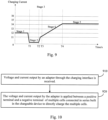
- the adapter in the constant current charging stage usually uses a multi-stage constant current charging method to charge.
- the multi-stage constant current charging may have M constant current stages (M is a positive integer not less than 2).
- the multi-stage constant current charging uses a predetermined charging current to start a first charging stage.
- the M constant current stages of the multi-stage constant current charging are sequentially executed from the first stage to the (M-1)th stage. After a previous constant current stage is changed to a next constant current stage in the constant current stages, the peak value or the average value of the current in the pulsating waveform can become smaller. When a battery voltage reaches a threshold voltage value for terminating charging, the previous constant current stage will change to the next constant current stage in the constant current stages.
- the current conversion process between two adjacent constant current stages may be gradual, or may be a stepped jump.
- terminal may include, but is not limited to, a device configured to be coupled via a wired connection (for example, via a public switched telephone network (PSTN), a digital subscriber line (DSL), a digital cable, a direct cable connection, and/or another data connection/network) and/or a device configured to receive/send a communication signal via a wireless interface (such as a cellular network, a wireless local area network (WLAN), a digital television network such as a DVB-H network, a satellite network, an AM-FM broadcast transmitter, and/or another communication terminal).
- PSTN public switched telephone network
- DSL digital subscriber line
- a digital cable a direct cable connection
- another data connection/network may include, but is not limited to, a device configured to receive/send a communication signal via a wireless interface (such as a cellular network, a wireless local area network (WLAN), a digital television network such as a DVB-H network, a satellite network, an AM-FM broadcast transmitter, and/or
- a terminal configured to communicate via a wireless interface may be referred to as a "wireless communication terminal", a “wireless terminal”, and/or a “mobile terminal”.
- mobile terminal include, but are not limited to, a satellite or cell phone; a personal communication system (PCS) terminal that can combine a cellular radiotelephone, data processing, facsimile, and data communications capabilities; may include a radiotelephone, a pager, an Internet/Intranet access, a Web browser, an electronic organizer, a calendar, and/or a personal digital assistant (PDA) equipped with a global positioning System (GPS) receiver; and a common laptop and/or palm type receiver or some other electronic devices including a transmitter-receiver radiotelephone.
- PCS personal communication system
- PDA personal digital assistant
- GPS global positioning System
- the charging current when the voltage in the pulsating waveform output from the adapter is directly applied to the battery of the chargeable device so as to charge the battery, the charging current is characterized by a pulsating wave, such as a clipped pulsating wave, and it is understood that the charging current charges the battery in an intermittent manner.
- a period of the charging current changes according to an input AC power, such as a frequency of an AC grid.
- a frequency corresponding to the period of the charging current is an integer multiple or a reciprocal of the frequency of the AC grid.
- a current waveform corresponding to the charging current may be composed of one pulse or one group of pulses synchronized with the grid.
- the battery can receive a pulsating direct current (direction unchanged, amplitude varying with time), an alternating current (both direction and amplitude varying with time), or a direct current (that is, a constant current, both amplitude and direction not varying with time) output from the adapter during the charging process (such as at least one of the trickle charging stage, the constant current charging stage, and the constant voltage charging stage).
- a direct current that is, a constant current, both amplitude and direction not varying with time
- the chargeable device usually uses a single cell.
- the single cell charged by higher charging current causes the chargeable device to generate more heat.
- the chargeable device of the present disclosure uses multiple cells coupled in series in lieu of single cell. The multiple cells are charged directly
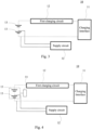
- FIG. 1 is a schematic diagram of a chargeable device according to a first embodiment, not covered by the claims, of the present disclosure.
- a chargeable device 10 includes a charging interface 11 and a first charging circuit 12, which are useable in the chargeable device of claim 1.
- the charging interface 11 is coupled to the first charging circuit 12.
- the first charging circuit 12 receives voltage and current outputted by an adapter through the charging interface 11. Additionally, the first charging circuit 12 loads the voltage and current outputted by the adapter onto two terminals of multiple cells 13 coupled in series arranged inside the chargeable device 10 directly. In other words, the first charging circuit 12 charges the multiple cells 13 directly.
- the multiple cells 13 are charged directly through the first charging circuit 12 in the present disclosure.
- the scheme of direct charging is good for decreasing generated heat to a certain degree.
- the chargeable device may be seriously overheated due to great current outputted by the adapter, such as current of 5A to 10A, which may be a security risk.
- a cell structure inside the chargeable device adopts multiple cells coupled in series based on the scheme of direct charging.
- a charging current necessary for the multiple cells is 1/N of the charging current necessary for the single cell where N indicates the number of cells of the multiple cells coupled in series built in the chargeable device.
- N indicates the number of cells of the multiple cells coupled in series built in the chargeable device.
- the 3000mAh single cell needs a 9A charging current to achieve the C-rate of 3C.
- 9A charging current to achieve the C-rate of 3C.
- two cells coupled in series, each with 1500mAh replace the single 3000mAh cell.
- the charging current of 4.5A just achieves the C-rate of 3C.
- the heat produced by the charging current of 4.5A is obviously less.
- the first charging circuit 12 charges the multiple cells 13 by direct charging so the voltage outputted by the adapter and received by the first charging circuit 12 needs to be greater than the total voltage applied to the multiple cells 13.
- the operating voltage of the single cell is between 3.0V and 4.35V.
- the voltage outputted by the adapter is set to be greater than or equal to 10V.
- the type of the charging interface 11 is not limited by the present embodiment of the present disclosure.
- a universal serial bus (USB) interface may be used.
- the USB interface may be a standard USB interface, a micro USB interface, or a Type-C interface.
- the first charging circuit 12 charges the multiple cells 13 through a power line in the USB port.
- the power line in the USB interface may be a VBus line and/or ground line in the USB port.
- the multiple cells 13 may be cells with uniform or similar specifications or parameters, which not only facilitates management but also improves overall performance and lifetime of the multiple cells 13.
- the multiple cells 13 in series can divide the voltage outputted by the adapter.
- a single cell is commonly applied to provide electricity in the chargeable device (or components or chips inside the chargeable device).
- the multiple cells 13 coupled in series are introduced in the present embodiment.
- the total voltage applied on the multiple cells 13 is greater so the multiple cells 13 is not suitable to provide electricity to the chargeable device (or the components or the chips inside the chargeable device).
- a possible method is to adjust the operating voltage of the chargeable device (or the components or the chips inside the chargeable device to support electricity supply to the multiple cells 13.
- this method affects the chargeable device sharply and produces a larger amount of costs.
- the present embodiment of the present disclosure details a method to solve the problem of electricity supply to the multiple cells 13.
- the chargeable device 10 may further include a step-down circuit 21 and a supply circuit 22 in some embodiments.
- An input terminal of the step-down circuit 21 is coupled to two terminals of the multiple cells 13.
- the step-down circuit 21 is configured to convert the total voltage across the multiple cells 13 into a first voltage V1 where a ⁇ V1 ⁇ b stands, a indicates the least operating voltage of the chargeable device 10 (the components inside the chargeable device 10 or the chip inside the chargeable device 10), and b indicates the maximum operating voltage of the chargeable device 10 (the components inside the chargeable device 10 or the chip inside the chargeable device 10).
- the supply circuit 22 is coupled to the output terminal of the step-down circuit 21. The supply circuit 22 supplies power to the chargeable device 10 based on the first voltage.
- the step-down circuit 21 is introduced based on the embodiment illustrated by Fig. 1 in the present disclosure.
- the chargeable device 10 operates, the total voltage across the multiple cells 13 is stepped down to a first voltage by the step-down circuit 21.
- the first voltage is ranged between the least operating voltage and the maximum operating voltage of the chargeable device 10 so the chargeable device 10 may be supplied with the first voltage directly. In this way, the problem of power supply with the multiple cells 13 is solved successfully.
- the total voltage across the multiple cells 13 varies with the electric volume of the multiple cells 13. Therefore, the total voltage across the multiple cells 13 may be the current total voltage across the multiple cells 13.
- the operating voltage of the single cell may range from 3.0 volts (V) to 4.35V.
- the multiple cells 13 includes two cells and that the current voltage of each of the two cells is 3.5V, the total voltage across the multiple cells 13 is 7V.
- the step-down circuit 21 may lower the total voltage across the multiple cells 13 to an arbitrary value ranging between 3.0V to 4.35V.
- the step-down circuit 21 may be a charge pump.
- the charge pump directly reduces the total voltage across the multiple cells 13 to 1/N of the present total voltage, where N indicates the number of cells of the multiple cells 13.
- a conventional buck circuit includes components such as a switch transistor and an inductor. Due to higher power loss of the inductor, using the buck circuit to step down voltage causes higher power loss due to higher power loss of the inductor.
- the charge pump utilizes switch transistors and capacitors to step down the voltage. Basically, the capacitor does not consume extra energy so the adoption of the charge pump helps reduce the loss of power in the process of stepping down the voltage.
- the switch transistor inside the charge pump controls charging and discharging of the capacitor in a certain way, and the input voltage reduces for a certain factor to obtain necessary voltage. (The factor chosen by the present disclosure is 1/N.)
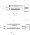
- the chargeable device 10 further includes a supply circuit 32.
- An input terminal of the supply circuit 32 is coupled to two terminals of any one cell of the multiple cells 13.
- the supply circuit 32 provides the components in the chargeable device 10 with electricity based on the voltage across the multiple cells 13.
- the voltage processed by the step-down circuit may occur ripples, affecting the quality of supplied power of the chargeable device 10.
- the supply voltage is from two terminals of any one cell of the multiple cells 13 directly to supply the components in the chargeable device 10 with electricity in the present disclosure. Since the supply voltage outputted by the cell is more stable, not only the scheme of providing electricity with the multiple cells works well, but also the quality of the supplied power of the chargeable device 10 is well maintained in the present disclosure.
- the chargeable device 10 further includes a balance circuit 33 coupled to the multiple cells 13.
- the balance circuit 33 is configured to balance the voltage across each of the multiple cells 13.
- one of the multiple cells 13 configured to supply electricity to the components inside the chargeable device 10 is called “primary cell", and the other cells called “secondary cells.”
- the primary cell continues consuming power after the power supply method illustrated in Fig. 3 is adopted, causing the voltage across the primary cell and the voltage across the secondary cell not to be balanced (or inconsistent). Imbalance of voltages across cells of the multiple cells 13 may influence overall performance negatively and affect the lifetime of the multiple cells 13 negatively. In addition, imbalance of voltages across cells of the multiple cells 13 makes it harder to manage the multiple cells 13 consistently. Therefore, the balance circuit 33 is used in the present disclosure to balance the voltages across cells of the multiple cells 13, to enhance the overall performance of the multiple cells 13, and to facilitate uniform management of the multiple cells 13.
- balance circuit 33 There are many ways of implementing the balance circuit 33. For example, using a load coupled to terminal of each cell to consume the electric volume of the secondary cell keeps the voltage across the secondary cell consistent with the voltage across the primary cell. Or, the primary cell is charged via the secondary cell until the voltage across the primary cell is consistent with the voltage across the secondary cell.
- the multiple cells 13 include a first cell 131 and a second cell 132.
- the electricity is transferred between the first cell 131 and the second cell 132 by capacitive coupling through the balance circuit 33.
- the voltages across the cells are balanced by capacitive coupling through the balance circuit 33, enhancing the overall performance of the multiple cells 13 in the present disclosure. In this way, the multiple cells 13 can be managed easily.
- the first cell 131 may be a secondary cell
- the second cell 132 may be a primary cell. Electricity in the first cell 131 can be transferred to the second cell 132 through the balance circuit 33.
- each of the first cell 131 and the second cell 132 may be a single cell, or two or more cells in series.
- the number of the cells is not limited in the present disclosure.
- a balance circuit 33 may include a first converting circuit 331, a first voltage adjustment circuit 3320, a first capacitive coupling circuit 333, and a second converting circuit 334, as illustrated in Fig. 11 .
- the first converting circuit 331 is configured to receive a direct voltage outputted by the first cell 131 and convert the direct current (DC) voltage outputted by the first cell into a first alternating current (AC) voltage.
- the first voltage adjustment circuit 3320 is configured to receive the first AC voltage and convert the first AC voltage into a second AC voltage.
- the amplitude of the second AC voltage is greater than the amplitude of the first AC voltage.
- the first capacitive coupling circuit 333 coupled to the second converting circuit 334, is configured to couple the second AC voltage to the second converting circuit 334 by capacitive coupling.
- the second converting circuit 334 converts the second AC voltage into a first charging voltage to charge the second cell 132.
- the first charge voltage may be a DC voltage.
- the first converting circuit 331 may include an inverter.
- the second converting circuit 334 may include a rectifier.
- the second converting circuit 334 may include a full-bridge rectifier or a rectifying diode.
- the first voltage adjustment circuit 3320 includes a first resonance circuit 332.
- the first resonance circuit 332 is configured to receive a first AC voltage and converts the first AC voltage into a second AC voltage by means of resonance, as Fig. 12 illustrates.
- the balance circuit 33 resonantly produces the second AC voltage and converts the second AC voltage into the first charging voltage to charge the second cell through the first capacitive coupling circuit 333 and the second converting circuit 334. Since the amplitude of the second AC voltage is greater than the amplitude of the first AC voltage, the efficiency of electricity transfer is enhanced.
- the balance circuit 33 resonantly increases the amplitude of the first AC voltage to obtain the second AC voltage in the present embodiment.
- the first resonance circuit 332 is characterized by simple structure, small area, and high reliability.
- the first resonance circuit 332 may include but is not limited to a multi-order resonance circuit or a one-order resonance circuit.
- Fig. 13 is a schematic diagram of a balance circuit according to another embodiment of the present disclosure.
- a first resonance circuit 332 may include a first inductor 41 and a first capacitor 42 coupled in series.
- a first capacitive coupling circuit 333 may include one or more capacitors. Input terminals of the first capacitive coupling circuit 333 are coupled to two terminals of the first inductor 41, as Fig. 13 illustrates. In another embodiment, input terminals of the first capacitive coupling circuit 333 are coupled to two terminals of the first capacitor 42.
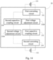
- Fig. 14 is a schematic diagram of a balance circuit according to another embodiment of the present disclosure. As Fig. 14 illustrates, the balance circuit further includes a second voltage adjustment circuit 3350 and a second capacitive coupling circuit 336.
- the second converting circuit 334 is further configured to receive the DC voltage outputted by the second cell and convert the DC voltage into a third alternating voltage.
- the second voltage adjustment circuit 3350 is configured to receive the third AC voltage and convert the third AC voltage into a fourth AC voltage.
- the amplitude of the fourth AC voltage is greater than the amplitude of the third AC voltage.
- the second capacitive coupling circuit 336 is configured to couple the fourth AC voltage to the first converting circuit 331 by capacitive coupling.
- the first converting circuit 331 converts the fourth AC voltage into a second charging voltage to charge the first cell 131.
- the balance circuit 33 supports electricity transfer from the first converting circuit 331 to the second converting circuit 334 and from the second converting circuit 334 to the first converting circuit 331. Not only a size of the balance circuit 33 is minimized but the efficiency of the balance circuit 33 for transferring electricity is raised.
- the second voltage adjustment circuit 3350 may include a second resonance circuit 335.
- the second resonance circuit 335 is configured to receive the third AC voltage and resonantly converts the third AC voltage into the fourth AC voltage, as illustrated in Fig. 15 .
- the balance circuit 33 supports electricity transfer from the first converting circuit 331 to the second converting circuit 334 and from the second converting circuit 334 to the first converting circuit 331. Not only is size of the balance circuit 33 is minimized but efficiency of the balance circuit 33 for transferring electricity is raised.
- the second charging voltage may be a DC voltage.
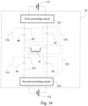
- the first resonance circuit 332 may include a first inductor 41 and a first capacitor 42, as illustrated in Fig. 16 .
- the second resonance circuit 335 may include the first inductor 41 and a second capacitor 44, as Fig. 16 illustrates.
- the first resonance circuit 332 and the second resonance circuit 335 may share the first inductor 41 to minimize size of the balance circuit, as Fig. 16 illustrates.
- Fig. 16 is a schematic diagram of a resonance circuit according to another embodiment of the present disclosure.
- a first resonance circuit 332 may include the first inductor 41 and the first capacitor 42.
- a second resonance circuit 335 may include the first inductor 41 and a second capacitor 44. In other words, the first resonance circuit 332 and the second resonance circuit 335 may share the first inductor 41.
- a first terminal of the first inductor 41 may be coupled to a first terminal of the first capacitor 42 and a first terminal of the second capacitor 44.
- a second terminal of the first capacitor 42 may be coupled to an input terminal of the first capacitive coupling circuit 333 or an input terminal of the second capacitive coupling circuit 336.
- the second terminal of the first capacitor 42 may be coupled to the first converting circuit 331.
- a second terminal of the second capacitor 44 may be coupled to the second converting circuit 334.
- the first capacitive coupling circuit 333 may include the second capacitor 44, and the second capacitive coupling circuit 336 may include the first capacitor 42.
- the first capacitive coupling circuit 333 may further include a third capacitor 46 and a switch K2.
- the second capacitive coupling circuit 336 may further include a fourth capacitor 48 and a switch K1.
- the switch K1 turns on and the switch K2 turns off
- the first resonance circuit 332 and the first capacitive coupling circuit 333 are operated while the third capacitor 46 is coupled to the first resonance circuit 332 and two terminals of the fourth capacitor 48 are short-circuited.
- the switch K1 turns off and the switch K2 turns on
- the second resonance circuit 335 and the second capacitive coupling circuit 336 operate while the two terminals of the third capacitor 46 are short-circuited and the fourth capacitor 48 is coupled to the second resonance circuit 335.
- the first converting circuit 331 is used as an inverter and a rectifier.
- the first converting circuit 331 may be a full-bridge rectifier. It is understood by one skilled in the art that the full-bridge rectifier may be used as an inverter as well.
- the second converting circuit 334 is used as an inverter and a rectifier.
- second converting circuit 334 may be a full-bridge rectifier. It is understood by one skilled in the art that the full-bridge rectifier may be used as an inverter as well.
- Fig. 17 illustrates a schematic diagram of the structure of a balance circuit 33 according to another embodiment of the present disclosure.
- the balance circuit 33 further includes a first control circuit 337.
- the first control circuit 337 controls the first voltage adjustment circuit 3320 and the first capacitive coupling circuit 333 to work to charge the second cell 132.
- the first control circuit 337 controls the second voltage adjustment circuit 3350 and the second capacitive coupling circuit 336 to work to charge the first cell 131.
- Fig. 18 illustrates a schematic diagram of the balance circuit according to the present embodiment of the present disclosure.
- the first cell 131 and the second cell 132 are coupled in series.
- the first converting circuit 331 may be a full-bridge rectifier.
- the first converting circuit 331 includes transistors Q1-Q4.
- the second converting circuit 334 may be a full-bridge rectifier.
- the second converting circuit 334 includes transistors Q5-Q8.
- the first resonance circuit 332 includes the first inductor 41 and the first capacitor 42.
- the first capacitive coupling circuit 333 includes the second capacitor 44 and the third capacitor 46.
- the balance circuit 33 may transfer the electricity unilaterally from the first cell 131 to the second cell 132 as illustrated in Fig. 18 .
- the first converting circuit 331 may be an inverter of other sorts, and the second converting circuit 334 may be a rectifier of other sorts.
- the number of the cells is not limited in the present disclosure.
- Fig. 19 illustrates a circuit diagram of a balance circuit according to another embodiment of the present disclosure.
- the first cell 131 and the second cell 132 are coupled in series.
- the first cell 131 may be a full-bridge rectifier.
- the first converting circuit 331 includes transistors Q1-Q4.
- the second converting circuit 334 may be a full-bridge rectifier.
- the second converting circuit 334 includes transistors Q5-Q8.
- the first resonance circuit 332 includes a first inductor 41 and a first capacitor 42.
- the first capacitive coupling circuit 333 includes a second capacitor 44 and a third capacitor 46.
- the second resonance circuit 335 includes a first inductor 41 and a second capacitor 44.
- the second capacitive coupling circuit 336 includes a first capacitor 42 and a fourth capacitor 48.
- the first capacitive coupling circuit 333 further includes a switch K1.
- the second capacitive coupling circuit 336 further includes a switch K2.
- the balance circuit can make a bilateral transfer of electricity between the first cell 131 and the second cell 132 come true, as illustrated in Fig. 19 .
- Fig. 19 Upon a condition that the voltage across the first cell 131 is greater than the voltage across the second cell 132, the switch K1 turns on and the switch K2 turns off. Therefore, the first resonance circuit 332 and the first capacitive coupling circuit 333 are controlled to operate, and the first cell 131 charges the second cell 132. Upon a condition that the voltage across the second cell 132 is greater than the voltage imposed on the first cell 131, the second resonance circuit 335 and the second capacitive coupling circuit 336 are controlled to operate, and the second cell 132 charges the first cell 131.
- the increase in the output power of the adapter may easily cause lithium precipitation when the cell inside the chargeable device is charged by the adapter. Accordingly, the lifetime of the cell is shortened.
- an adapter is controlled to output a pulsating direct current (or called “unidirectional pulsating output current,” “pulsating waveform current,” or “pulsating current with a clipped waveform”) in some embodiments.
- the first charging circuit 12 charges the multiple cells 13 by direct charge so the pulsating direct current outputted by the adapter can be applied to two terminals of the multiple cells 13 directly.
- the pulsating direct current alternates periodically.
- the pulsating direct current can reduce lithium precipitation of a cell and enhance the lifetime of the cell.
- the pulsating direct current can lower the probability and strength of an arc of a trigger point of a charging interface and increase the lifespan of the charging interface.
- an output current of the adapter is a pulsating direct current.
- an output current of the adapter is a pulsating direct current without a primary filter circuit and a secondary filter circuit in the adapter.
- a first charging circuit 12 receives an alternating current outputted by an adapter (for example, to remove a primary filter circuit, a secondary rectifier, and a secondary filter circuit in the adapter to obtain an alternating current outputted by the adapter).
- the alternating current reduces the possibility of lithium precipitation as well, which help enhance the lifetime of the cell.
- the voltage and current received by the first charging circuit 12 from the adapter through the charging interface 11 may be the voltage and current outputted by the adapter under a constant current mode (constant current charging mode or a constant current charging stage).
- the multiple cells 13 may be packaged in a battery 51 as well in some embodiments, as Fig. 6 illustrates.
- the battery 51 further includes a cell protection plate 52.
- the battery 51 has functions of over-voltage and over-current protection, electricity balance management, electricity management.
- the multiple cells 13 may be packaged in a plurality of batteries 51 in some embodiments.
- the chargeable device 10 further includes a second charging circuit 61, as illustrated in Fig. 7 .
- the second charging circuit 61 includes a voltage boost circuit 62. Two terminals of the voltage boost circuit 62 are coupled to a charging interface 11 and a multiple cells 13 correspondingly.
- the voltage boost circuit 62 receives voltage outputted by an adapter through the charging interface 11, and the voltage outputted by the adapter is elevated to be the second voltage.
- the second voltage is applied onto the two terminals of the multiple cells 13 to charge the multiple cells 13.
- the voltage outputted by the adapter and received by the second charging circuit 61 is less than the total voltage of the multiple cells 13.
- the second voltage is greater than the total voltage of the multiple cells 13.
- the multiple cells 13 are charged directly through the first charging circuit 12. Based on the direct charging method, the voltage outputted by the adapter needs to be greater than the total voltage of the multiple cells 13. For example, provided that two cells are coupled in series and present voltage of each cell is 4V, the voltage outputted by the adapter needs to be 8V or more. However, the output voltage of a standard adapter (as the associated adapter mentioned above) is 5V so it is impossible to charge the multiple cells 13 through the first charging circuit 12.
- the second charging circuit 61 is provided in the present invention.
- the second charging circuit 61 includes a voltage boost circuit 62.
- the voltage boost circuit 62 is configured to elevate the voltage outputted by the adapter to be the second voltage.
- the voltage outputted by the adapter is greater than the total voltage of the multiple cells 13. In this way, the problem that a standard adapter fails to charge the multiple cells 13 coupled in series is well solved.
- the voltage outputted by the adapter and received by the second charging circuit 61 is not limited by the present embodiment of the present disclosure. As long as the voltage outputted by the adapter is less than the total voltage of the multiple cells 13, the multiple cells 13 can be charged by elevated voltage through the second charging circuit 61.
- the voltage boost circuit 62 is not limited by the present embodiment.
- a boost circuit is adopted, or a charge pump is configured to raise voltage.
- the second charging circuit 61 may adopt a conventional design of the charging circuit in some embodiments; that is, a converting circuit (such as a charging integrated circuit) is arranged between the charging interface and the cell.
- the converting circuit may control the adapter to keep constant voltage and constant current in the process of charging and adjust the voltage outputted by the adapter according to practical demands such as raising voltage or lowering voltage.
- the voltage outputted by the adapter is raised over the second voltage of the total voltage of the multiple cells 13 by using the function of raising voltage of the multiple cells 13 in the present embodiment.
- switch between the first charging circuit 12 and the second charging circuit 61 may be realized through a switch and a control circuit.
- a control circuit is arranged inside the chargeable device , and the control circuit may swiftly switch between the first charging circuit 12 and the second charging circuit 61 according to practical demands (the type of the adapter).
- an adapter supports a first charging mode and a second charging mode in some embodiments.
- the adapter charges the chargeable device operable in the second charging mode faster than the adapter charges the chargeable device on the first charging mode.
- an adapter charges multiple cells 13 through the second charging circuit 61 by the first charging mode in some embodiments. Besides, the adapter charges the multiple cells 13 through the first charging circuit 12 by the second charging mode. In other words, it takes less time for the adapter to charge the battery with the same electricity volume operable in the second charging mode compared with the adapter on the first charging mode.
- the first charging mode may be a normal charging mode.
- the second charging mode may be a fast charging mode.
- the normal charging mode means that the adapter outputs a comparably smaller amount of current (usually less than 2.5A) or a comparably smaller amount of power (usually less than 15W) to charge a battery in the chargeable device. It usually takes several hours to fill up a battery with a larger amount (like with an amount of 3000 milliampere) on the normal charging mode.
- the adapter outputs a comparably larger amount of current (usually greater than 2.5A, like 4.5A, 5A, or more) or a comparably larger amount of power (usually more than or equal to 15W) to charge the battery in the chargeable device by the fast charging mode.
- the charging rate of the adapter is faster on the fast charging mode so it takes less time to full up a battery with the same volume obviously.
- the charging interface 11 may include a data line, as Fig. 8 illustrates.
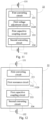
- the chargeable device 10 may further include a control circuit 71.
- the control circuit 71 may communicate with the adapter bidirectionally through the data line to control the output of the adapter operable in the second charging mode. Take the charging interface as a USB port for example.
- the data line may be a D+ line and/or D- line in the USB port.
- the present disclosure does not limit the communicative contents between the control circuit 71 of the adapter and the chargeable device.
- the present disclosure does not limit how the control circuit 71 controls the output of the adapter operable in the second charging mode.
- the control circuit 71 can communicate with the adapter, interact the present total voltage of the multiple cells 13 with the present total electricity of the multiple cells 13 in the chargeable device 10, and adjust the voltage or current outputted by the adapter based on the present total voltage or the present total electricity of the multiple cells 13.
- Interaction between the control circuit 71 and the adapter and the method of controlling the output of the adapter operable in the second charging mode are detailed as follows.
- the present disclosure does not limit priority and subordination of the adapter and the chargeable device (or the control circuit 71 of the chargeable device ).
- either one of the adapter or the chargeable device acts as a primary device and actively communicates with the other.
- the other acts as a secondary device and offers a first reply or a first response to the communication from the primary device.
- the voltage level of the adapter and the voltage level of the chargeable device are compared with the voltage level of ground in the process of communication to ensure which one is primary device and which one is the secondary device.
- the present disclosure does not limit priority and subordination of the adapter and the chargeable device.
- either one of the adapter or the chargeable device acts as a primary device and actively communicates with the other.
- the other acts as a secondary device and offers a first reply or a first response to the communication from the primary device.
- the primary device offers a second reply or a second response in response to the first reply or the first response from the secondary device. Therefore, the negotiation process of a charging mode between the adapter and the chargeable device is finished.
- a charging operation between the primary device and the secondary device is performed to ensure safe and reliable performance of the charging.
- the primary device may offer the second response or the second reply based on the first response or the first reply from the secondary device in communication.
- One method may include: The primary device can receive the first response or the first reply from the secondary device in communication and offer the second response or the second reply based on the first response or the first reply from the secondary device accordingly. For example, when the primary device receives the first response or the first reply from the secondary device in communication within the predetermined time, the primary device offers the second response or the second reply based on the first response or the first reply from the secondary device.
- the negotiation process of a charging mode between the primary device and the secondary device is finished. The primary device and the secondary device perform the charging on the first charging mode or the second charging mode based on the negotiation result. That is, the adapter charges the chargeable device on the first charging mode or the second charging mode based on the negotiation result.
- the primary device may offer the second response or the second reply based on the first response or the first reply from the secondary device in communication.
- Another method may include: The primary device does not receive the first response or the first reply from the secondary device in communication but still offers the second response or the second reply based on the first response or the first reply from the secondary device accordingly. For example, when the primary device does not receive the first response or the first reply from the secondary device in communication within the predetermined time, the primary device still offers the second response or the second reply based on the first response or the first reply from the secondary device.
- the negotiation process of a charging mode between the primary device and the secondary device is finished. The primary device and the secondary device perform the charging by the first charging mode or the second charging mode based on the negotiation result. That is, the adapter charges the chargeable device by the first charging mode or the second charging mode based on the negotiation result.
- a chargeable device starts to communicate, and an adapter, as a secondary device, offers a first reply or a first response in response to the primary device's communication. Afterwards, the chargeable device does not need to offer a second reply or a second response in response to the adapter's first reply or first response accordingly. Therefore, the negotiation process of a charging mode between the adapter and the chargeable device is finished. Further, the adapter can charge the chargeable device either by the first charging mode or by the second charging mode based on the negotiation result.
- control circuit 71 when the control circuit 71 communicates with an adapter bidirectionally through a data line to control the output of the adapter by the second charging mode, the control circuit 71 communicates with the adapter bidirectionally to negotiate the charging mode between the adapter and the chargeable device.
- control circuit 71 when the control circuit 71 communicates with an adapter bidirectionally to negotiate the charging mode between the adapter and the chargeable device , the control circuit 71 receives a first instruction sent by the adapter, the first instruction being configured to inquire whether the chargeable device enables the second charging mode; the control circuit 71 also sends a reply instruction responsive to the first instruction to the adapter, and the reply instruction responsive to the first instruction being configured to ask the chargeable device whether to allow to enable the second charging mode; and the control circuit 71 further controls the adapter to charge the multiple cells through the first charging circuit 12 on condition that the chargeable device agrees to enable the second charging mode.
- control circuit 71 when the control circuit 71 communicates with an adapter bidirectionally through a data line to control the output process of the adapter by the second charging mode, the control circuit 71 communicates with the adapter bidirectionally to ensure a charging current outputted by the adapter operable in the second charging mode and configured to charge a chargeable device.
- control circuit 71 when the control circuit 71 communicates with an adapter bidirectionally to ensure a charging voltage outputted by the adapter operable in the second charging mode and configured to charge a chargeable device , the control circuit 71 receives a second instruction sent by the adapter; the second instruction being configured to inquire whether the voltage outputted by the adapter matches the present total voltage of the multiple cells 13; the control circuit 71 further sends a reply instruction responsive to the second instruction to the adapter, the reply instruction responsive to the second instruction being configured command the voltage outputted by the adapter to match the present total voltage of the multiple cells 13 or to make the voltage outputted by the adapter and the present total voltage of the multiple cells 13 higher or lower.
- the second instruction may be configured to inquire whether the present voltage outputted by the adapter acting as a charging voltage for the chargeable device is suitable operable in the second charging mode.
- the reply instruction responsive to the second instruction may be configured to command the voltage outputted by the adapter to match the present total voltage of the multiple cells 13 or to make the voltage outputted by the adapter and the present total voltage of the multiple cells 13 higher or lower.
- the present output voltage of the adapter matching the present total voltage of the multiple cells 13 or the present output voltage of the adapter acting as the charging voltage for the chargeable device suitable operable in the second charging mode means that the present output voltage of the adapter is slight greater than the present total voltage of the multiple cells 13 and that the difference between the output voltage of the adapter and the present total voltage of the multiple cells 13 is within a predetermined range (usually order of magnitude of hundreds of millivolts).
- control circuit 71 when the control circuit 71 communicates with an adapter bidirectionally through the data line to control the output of the adapter operable in the second charging mode, the control circuit 71 communicates with the adapter bidirectionally to ensure a charging current outputted by the adapter operable in the second charging mode and configured to charge a chargeable device.
- control circuit 71 when the control circuit 71 communicates with an adapter bidirectionally to ensure a charging current outputted by the adapter operable in the second charging mode and configured to charge a chargeable device , the control circuit 71 receives a third instruction sent by the adapter; the third instruction being configured to inquire the maximum charging current for the chargeable device currently; the control circuit 71 further sends a reply instruction responsive to the third instruction to the adapter, the reply instruction responsive to the third instruction being configured to command the maximum charging current for the chargeable device currently to ensure the charging current outputted by the second adapter for the chargeable device operable in the second charging mode based on the maximum charging current for the chargeable device currently.
- the maximum charging current for the chargeable device currently there are many charging methods for the maximum charging current for the chargeable device currently to ensure the charging current outputted by the second adapter for the chargeable device operable in the second charging mode based on the maximum charging current for the chargeable device currently for the control circuit 71.
- the second adapter ensures that the maximum charging current for the chargeable device currently is for the charging current for the chargeable device.
- the charging current outputted by the second adapter operable in the second charging mode for the chargeable device is ensured after the maximum charging current for the chargeable device currently and the capacity of current output are taken into considerations.
- control circuit 71 when the control circuit 71 communicates with an adapter bidirectionally through the data line to control the output of the second adapter operable in the second charging mode, the control circuit 71 communicates with the adapter bidirectionally operable in the second charging mode to adjust a current outputted by the adapter.
- control circuit 71 when the control circuit 71 communicates with an adapter bidirectionally to adjust a current outputted by the adapter, the control circuit 71 receives a fourth instruction sent by the adapter, the fourth instruction being configured to inquire the present total voltage of the multiple cells; the control circuit 71 further sends a reply instruction responsive to the fourth instruction to the adapter, and the reply instruction responsive to the fourth instruction being configured to indicate the present total voltage of the multiple cells.
- the adapter can adjust the current output based on the present total voltage of the multiple cells.
- control circuit 71 is further configured to receive a fifth instruction sent by an adapter.
- the fifth instruction is configured to indicate that there is a bad contact of the control circuit 71.
- the present embodiment details a communication process between the adapter and the chargeable device (specifically performed by the control circuit inside the chargeable device ). It is understood that the example shown in Fig. 9 merely help a person skilled in the art understand the present embodiment rather than limit the number of scenes. A person skilled in the art can modify or change the embodiment correspondingly according to the example shown in Fig. 9 . Such modifications or changes are within the scope of the present embodiment.
- the communication process (or called “fast communication process”) between the adapter and the chargeable device may include Stage 1, Stage 2, Stage 3, Stage 4, and Stage 5.
- the chargeable device may detect the type of power supply device via data lines D+ and D-.
- the chargeable device detects the power supply device to be the adapter
- the current absorbed by the chargeable device is greater than the predetermined current threshold I2 (such as 1A).
- the adapter detects the current outputted by the adapter greater than or equal to the predetermined current threshold I2 within the predetermined duration (for example, a continuous T1 duration)
- the adapter may regard the type of the power supply device is recognized by the chargeable device.
- the adapter starts to negotiate with the chargeable device and sends Instruction 1 (corresponding to the above-mentioned first instruction) to the chargeable device to inquire whether the chargeable device agrees the adapter to charge the chargeable device operable in the second charging mode.
- the adapter When the adapter receives the reply instruction responsive to Instruction 1 sent by the chargeable device, and the reply instruction responsive to Instruction 1 indicates that the chargeable device does not agree the adapter to charge the chargeable device operable in the second charging mode, the adapter detects the output current of the adapter again. When the current outputted by the adapter is still greater than or equal to I2 in a predetermined continuous duration (for example, a continuous T1 duration), the adapter sends the reply instruction responsive to Instruction 1 to the chargeable device again. The adapter inquires the chargeable device to agree to charge the chargeable device with the adapter operable in the second charging mode. The adapter repeats the operation at Stage 1 until the chargeable device agrees the adapter to charge the chargeable device operable in the second charging mode or the current outputted by the adapter no longer satisfies the requirement of the output current greater than or equal to I2.
- a predetermined continuous duration for example, a continuous T1 duration
- the communication process enters Stage 2.
- the voltage outputted by the adapter may include a plurality of levels.
- the adapter sends instruction 2 to the chargeable device (corresponding to the second instruction) to inquire whether the voltage outputted by the adapter (the present output voltage) matches the present total voltage of the multiple cells (the present total voltage of the multiple cells).
- the chargeable device sends the reply instruction responsive to Instruction 2 to indicate that the voltage outputted by the adapter matches the present total voltage of the chargeable device (the present total voltage of the multiple cells), the voltage outputted by the adapter is greater than or less than the present total voltage of the chargeable device (the present total voltage of the multiple cells). If the reply instruction responsive to Instruction 2 is to make the voltage outputted by the adapter and the present total voltage of the chargeable device (the present total voltage of the multiple cells) higher or lower, the adapter can adjust one level of the voltage outputted by the adapter and sends the reply instruction responsive to Instruction 2 to the chargeable device to inquire whether the voltage outputted by the adapter matches the present voltage (the present total voltage of the multiple cells) of the battery again. The operation at Stage 2 are repeated until the chargeable device ensures that the voltage outputted by the adapter matches the present voltage (the present total voltage of the multiple cells) of the battery. Afterwards, Stage 3 starts.
- the adapter sends Instruction 3 (corresponding to the above-mentioned the third instruction) and inquires the maximum charging current supported by the chargeable device currently.
- the chargeable device sends the reply instruction responsive to Instruction 3 to the adapter to indicate the maximum charging current supported by the chargeable device currently. Afterwards, Stage 4 starts.
- Stage 5 Based on the maximum charging current supported by the chargeable device currently, the charging current outputted by the adapter to charge the chargeable device operable in the second charging mode. Afterwards, Stage 5 starts, that is, constant current charging stage.
- the adapter When entering the constant current charging stage, the adapter sends Instruction 4 (corresponding to the above-mentioned fourth instruction) to the chargeable device every interval of time and inquire the present voltage (e.g. the total voltage of the multiple cells) of the battery of the chargeable device.
- the chargeable device sends the reply instruction responsive to Instruction 4 to the adapter to feedback the present voltage (the total voltage of the multiple cells) of the battery.
- the adapter can detect whether the connection of the charging interface is normal based on the present voltage (the total voltage of the multiple cells) of the battery and whether the current outputted by the adapter needs lower.
- the chargeable device sends Instruction 5 (corresponding to the above-mentioned fifth instruction), the adapter retreats from the second charging mode, resets to enter Stage 1.
- a chargeable device sends a reply instruction responsive to Instruction 1 at Stage 1.
- the reply instruction responsive to Instruction 1 may attach data (or information) of a path impedance of the chargeable device.
- the connection of the charging interface is detected to be normal with the path impedance of the chargeable device at Stage 5.
- a time period from the time that the chargeable device agrees the adapter charging the chargeable device operable in the second charging mode until the time that an output voltage of the adapter is adjusted to a suitable charging voltage, may be set as a predetermined time period at Stage 2. If the time goes beyond the predetermined time period, the adapter or the chargeable device is detected to be abnormal in the communication process and then resets to enter Stage 1.
- the voltage outputted by the adapter is higher than the present voltage of the battery of the chargeable device (the present total voltage of the multiple cells) by ⁇ V ( ⁇ V can range from 200 mV to 500 mV) at Stage 2.
- the chargeable device may send a reply instruction responsive to Instruction 2 to the adapter to indicate that the voltage outputted by the adapter matches the voltage of the battery of the chargeable device (the present total voltage of the multiple cells).
- the adjustment speed of a current outputted by an adapter can be controlled within limits at Stage 4. In this way, the charging process will not be abnormal once the adjustment speed is a bit high.
- a variation of a current outputted by an adapter is controlled within five percent (5%) of the output current at Stage 5.
- an adapter can detect a path impedance of a charging circuit in real time at Stage 5. Specifically, the adapter can detect the path impedance of the charging circuit based on an output voltage and an output current of the adapter and the present voltage (present total voltage of the multiple cells) of the battery feedback by the chargeable device. Since "path impedance of charging circuit" greater than "path impedance of charging circuit plus impedance of charging cable" indicates a bad contact of a charging interface, the adapter stops charging the chargeable device operable in the second charging mode.
- communication interval between the adapter and the chargeable device is controlled within limits to prevent abnormality from occurring in the communication process because the interval is too short.
- termination of the charging process may be divided into recoverable termination and unrecoverable termination.
- the charging process terminates, the charging communication process resets, and the charging process enter Stage 1 again. Afterwards, the charging process enters Stage 2 if the chargeable device does not agree the adapter to charge the chargeable device operable in the second charging mode.
- Such kind of termination of the charging process is regarded as unrecoverable termination.
- the charging process terminates, the charging communication process resets, and the charging process enters Stage 1 again.
- the chargeable device agrees the adapter to charge the chargeable device operable in the second charging mode to recover the charging process.
- Such kind of termination of the charging process may be regarded as recoverable termination.
- the chargeable device detects the battery (the multiple cells) is abnormal, the charging process terminates, the charging process resets, and the charging process enters Stage 1 again. Afterwards, the chargeable device does not agree the adapter to charge the chargeable device operable in the second charging mode. When the battery (the multiple cells) becomes normal again, and the requirement of Stage 1 is fulfilled, the chargeable device agrees the adapter to charge the chargeable device operable in the second charging mode.
- Such kind of termination of the charging process may be regarded as recoverable termination.
- Fig. 9 The blocks or operations illustrated in Fig. 9 are merely an exemplary.
- handshake communication between the chargeable device and the adapter may be launched by the chargeable device as well; that is the chargeable device sends Instruction 1 and inquires whether the adapter enables the second charging mode.
- the chargeable device receives the reply instruction responsive to the adapter to command the adapter to agree to charge the chargeable device by the second charging mode, the adapter starts to charge the battery (the multiple cells) of the chargeable device by the second charging mode.
- a stage of constant voltage charging may be further included after Stage 5 finishes.
- the chargeable device feedbacks the present voltage of the battery (the present total voltage of the multiple cells) to the adapter at Stage 5.
- the present voltage of the battery the present total voltage of the multiple cells
- the chargeable device is charged by a constant voltage from the constant current.
- the charging current gradually lessens.
- the battery (the multiple cells) of the chargeable device is filled and the charging process stops.
- the device proposed by the present disclosure is detailed, as shown Fig. 1 to Fig. 9 .
- the method proposed by the present disclosure is detailed, as shown Fig. 10 . It is understood that the description of the method and the description of the device correspond to each other. For simplicity, some repetitions are omitted.
- Fig. 10 illustrates a flowchart of a charging method according to one embodiment, not covered by the claims, of the present disclosure.
- the chargeable device including a charging interface is charged by the charging method as illustrated in Fig. 10 .
- the charging method according to the present invention includes block 910 and block 920 among other features.
- the voltage and current outputted by the adapter is applied between a positive terminal and a negative terminal of multiple cells coupled in series built in the chargeable device to directly charge the multiple cells.
- the charging method illustrated in Fig. 10 further includes: electrical power suitable for the components of the chargeable device is supplied based on the voltage of the selected one of the multiple cells.
- the charging method further includes: voltage of each cell of the multiple cells is balanced.
- the multiple cells include a first cell and a second cell.
- a process that the voltage of each cell of the multiple cells is balanced includes: electricity between the first cell and the second cell is transferred by capacitive coupling.
- a process that the electricity between the first cell and the second cell is transferred by capacitive coupling includes: a direct current (DC) voltage outputted by the first cell is received and the DC voltage outputted by the first cell is converted into a first alternating current (AC) voltage.
- the process also includes the first AC voltage is received, the first AC voltage into a second AC voltage is converted, the second AC voltage is conducted to a second converting circuit by capacitive coupling, and the second AC voltage is converted into a first charging voltage to charge the second cell by the second converting circuit.
- An amplitude of the second AC voltage is greater than an amplitude of the first AC voltage.
- a process that the first AC voltage is converted into the second AC voltage includes: the first AC voltage is resonantly converted into the second AC voltage.
- the charging method as illustrated in Fig. 10 further includes: DC voltage outputted by the second cell is received, the DC voltage outputted by the second cell is converted into a third AC voltage, the third AC voltage is received and the third AC voltage is converted into a fourth AC voltage, converting, the fourth AC voltage is conducted to a first converting circuit by capacitive coupling, and the fourth AC voltage is converted into a second charging voltage to charge the first cell by the first converting circuit.
- An amplitude of the fourth AC voltage is greater than an amplitude of the third AC voltage.
- a process that the third AC voltage is converted into the fourth AC voltage includes: the third AC voltage is resonantly converted into the fourth AC voltage.
- a process that the first AC voltage is resonantly converted into the second AC voltage includes: the first AC voltage is resonantly converted into the second AC voltage by a first inductor and a first capacitor.
- a process that the third AC voltage is resonantly converted into the fourth AC voltage includes: the third AC voltage is resonantly converted into the fourth AC voltage by the first inductor and a second capacitor.
- the charging method as illustrated in Fig. 10 further includes: the second cell is charged when the voltage of the first cell is greater than the voltage of the second cell, and the first cell is charged when the voltage of the second cell is greater than the voltage of the first cell.
- the charging method further includes: the voltage outputted by the adapter through the charging interface is converted to second voltage, and the second voltage is applied between the positive terminal and the negative terminal to charge the multiple cells.
- the second voltage is greater than a total voltage of the multiple cells.
- the adapter supports a first charging mode and a second charging mode.
- a charging rate of charging the chargeable device operable in the second charging mode is faster than a charging rate of charging the chargeable device operable in the second charging mode.
- the charging interface includes a data line.
- the charging method as illustrated in Fig. 9 further includes: the adapter is bidirectionally communicated with the chargeable device through the data line to control output of the adapter operable in the second charging mode.
- a process that the adapter is bidirectionally communicated with the chargeable device through the data line to control output of the adapter operable in the second charging mode includes: the adapter is bidirectionally communicated with the chargeable device to negotiate a charging mode between the adapter and the chargeable device.
- a process that the adapter is bidirectionally communicated with the chargeable device to negotiate a charging mode between the adapter and the chargeable device includes: a first instruction sent by the adapter is received, a reply instruction responsive to the first instruction is sent to the adapter, and the adapter is controlled to charge the multiple cells through the first charging circuit upon a condition that the chargeable device agrees to enable the second charging mode.
- the first instruction is configured to inquire whether the chargeable device enables the second charging mode.
- the reply instruction responsive to the first instruction is configured to ask the chargeable device whether to agree to enable the second charging mode.
- a process that the adapter is bidirectionally communicated with the chargeable device through the data line to control output of the adapter operable in the second charging mode includes: the adapter is bidirectionally communicated with the chargeable device to ensure a charging voltage outputted by the adapter operable in the second charging mode to charge the chargeable device.
- a process that the adapter is bidirectionally communicated with the chargeable device to ensure a charging voltage outputted by the adapter operable in the second charging mode to charge the chargeable device includes: a second instruction sent by the adapter is received, and a reply instruction responsive to the second instruction is sent to the adapter.
- the second instruction is configured to inquire whether the voltage outputted by the adapter matches a present total voltage of the multiple cells.
- the reply instruction responsive to the second instruction is configured to indicate that the voltage outputted by the adapter matches the present total voltage of the multiple cells, the voltage outputted by the adapter is greater than the present total voltage of the multiple cells, or the voltage outputted by the adapter is less than the present total voltage of the multiple cells.
- a process that the adapter is bidirectionally communicated with the chargeable device through the data line to control output of the adapter operable in the second charging mode includes: the adapter is bidirectionally communicated with the chargeable device to ensure a charging current outputted by the adapter operable in the second charging mode to charge the chargeable device.
- a process that the adapter is bidirectionally communicated with the chargeable device to ensure a charging current outputted by the adapter operable in the second charging mode to charge the chargeable device includes: a third instruction sent by the adapter is received, and a reply instruction responsive to the third instruction is sent to the adapter.
- the third instruction is configured to inquire a maximum charging current for the chargeable device.
- the reply instruction responsive to the third instruction is configured to indicate the maximum charging current for the chargeable device to ensure the charging current outputted by the adapter for the chargeable device operable in the second charging mode based on the maximum charging current for the chargeable device.
- a process that the adapter is bidirectionally communicated with the chargeable device through the data line to control output of the adapter operable in the second charging mode includes: the adapter is bidirectionally communicated with the chargeable device to adjust the current outputted by the adapter in a charging process operable in the second charging mode.
- a process that the adapter is bidirectionally communicated with the chargeable device to adjust the current outputted by the adapter in a charging process operable in the second charging mode a fourth instruction sent by the adapter is received, and a reply instruction responsive to the fourth instruction is sent to the adapter.
- the fourth instruction is configured to inquire the present total voltage of the multiple cells.
- the reply instruction responsive to the fourth instruction is configured to indicate the present total voltage of the multiple cells.
- the adapter adjusts an outputted charging current based on the reply instruction responsive to the fourth instruction and indicative of the present total voltage of the multiple cells.
- the revealed system, device and method may be implemented in other ways.
- the abovementioned embodiments of the device are merely schematic.
- the division of the units is merely a division based on logical functions; it may be different when they are put into practice.
- a plurality of units or components may be combined or integrated into another system, or some features may be ignored or not be performed.
- the displayed or discussed coupling, direct coupling or communication can be done through some interfaces, devices, or indirect coupling or communication between units; they may be electrical, mechanical, or in other forms.
- the units described as separated parts may or may not be physically separated.
- a part that appeared as a unit may or may not be a physical unit, i.e. it can locate in one place, or it can be distributed to multiple network units. Part of or all of the units can be selected based on actual needs to achieve the object of the solutions of the present embodiments.
- each of the functional units in the embodiments of the present disclosure may be integrated in one processing unit, or may be independent units physically separated, or may integrate with another one or more units and appear as a single unit.
- the function is realized as a software functional unit and used or sold as a standalone product, it may be stored in a computer-readable storage medium. Based on such understanding, the technical solutions of the present disclosure per se, or its contribution to the related art, or the technical solution may be realized in a software product.
- the computer software product is stored in a storage medium, including several commands that enable a computer device (may be a personal computer, a server, or network device) to perform all or part of the steps of the methods of the various embodiments of the present disclosure.
- the storage medium includes U-disk, removable hard disk, read-only memory (ROM), random access memory (RAM), magnetic disk or compact disc (CD) and other medium that can store program codes.
Landscapes
- Engineering & Computer Science (AREA)
- Power Engineering (AREA)
- Manufacturing & Machinery (AREA)
- Chemical & Material Sciences (AREA)
- Chemical Kinetics & Catalysis (AREA)
- Electrochemistry (AREA)
- General Chemical & Material Sciences (AREA)
- Charge And Discharge Circuits For Batteries Or The Like (AREA)
- Secondary Cells (AREA)
- Crystals, And After-Treatments Of Crystals (AREA)
Claims (14)
- Ladbare Vorrichtung (10), umfassend:eine Ladeschnittstelle (11),eine erste Ladeschaltung (12), die mit der Ladeschnittstelle (11) gekoppelt und dafür gestaltet ist, über die Ladeschnittstelle (11) Spannung und Strom zu empfangen, die von einem Adapter ausgegeben werden, und die von dem Adapter ausgegebene Spannung und den von dem Adapter ausgegebenen Strom zwischen einem positiven Anschluss und einem negativen Anschluss mehrerer Zellen (13) anzulegen, die in Reihe geschaltet und in die ladbare Vorrichtung (10) eingebaut sind, um die mehreren Zellen (13) direkt zu laden, wenn die von dem Adapter ausgegebene Spannung größer als die Gesamtspannung der mehreren Zellen (13) ist, wobei die mehreren Zellen (13) eine erste Zelle (131) und eine zweite Zelle (132) umfassen,eine zweite Ladeschaltung (61), die eine Spannungserhöhungsschaltung (62) umfasst, die zwischen die Ladeschnittstelle (11) und die mehreren Zellen (13) geschaltet ist,wobei die Spannungserhöhungsschaltung (62) dafür gestaltet ist, die von dem Adapter ausgegebene Spannung in eine zweite Spannung umzuwandeln, wobei die zweite Spannung zwischen dem positiven Anschluss und dem negativen Anschluss der mehreren Zellen (13) angelegt wird, um die mehreren Zellen (13) zu laden, wenn der von dem Adapter ausgegebene Spannungswert geringer als eine Gesamtspannung der mehreren Zellen (13) ist, und der zweite Spannungswert größer als die Gesamtspannung der mehreren Zellen (13) ist,dadurch gekennzeichnet, dass,wenn die erste Ladeschaltung (12) verwendet wird, die mehreren Zellen (13) dafür gestaltet sind, unter Verwendung eines Ladestroms I/N für die mehreren Zellen so schnell wie eine einzelne Zelle mit einer Kapazität C, einem Ladestrom I und einer Spannung V geladen zu werden, wobei die Kapazität jeder Zelle der mehreren Zellen C/N beträgt und die Spannung jeder Zelle der mehreren Zellen V beträgt, wobei N die Anzahl von Zellen der mehreren Zellen angibt, und dadurch, dassdie ladbare Vorrichtung ferner eine Ausgleichsschaltung (33) umfasst, die mit den mehreren Zellen (13) gekoppelt und dafür gestaltet ist, die Spannung zwischen den mehreren Zellen (13) auszugleichen.
- Ladbare Vorrichtung (10) nach Anspruch 1, wobei die Ausgleichsschaltung (33) Folgendes umfasst:eine erste Wandlungsschaltung (331), die dafür gestaltet ist, eine Gleichspannung zu empfangen, die von der ersten Zelle (131) ausgegeben wird, und die von der ersten Zelle (131) ausgegebene Gleichspannung in eine erste Wechselspannung umzuwandeln,eine erste Spannungsjustierungsschaltung (3320), die dafür gestaltet ist, die erste Wechselspannung zu empfangen und die erste Wechselspannung in eine zweite Wechselspannung umzuwandeln, wobei eine Amplitude der zweiten Wechselspannung größer ist als eine Amplitude der ersten Wechselspannung,eine erste kapazitive Kopplungsschaltung (333) und eine zweite Wandlungsschaltung (336), wobei die erste kapazitive Kopplungsschaltung (333) dafür gestaltet ist, die zweite Wechselspannung kapazitiv mit der zweiten Wandlungsschaltung (336) zu koppeln, wobei die zweite Wandlungsschaltung (336) dafür gestaltet ist, die zweite Wechselspannung in eine erste Ladespannung umzuwandeln, um die zweite Zelle (132) zu laden.
- Ladbare Vorrichtung (10) nach Anspruch 2, wobei die erste Spannungsjustierungsschaltung (3320) eine erste Resonanzschaltung umfasst, die dafür gestaltet ist, die erste Wechselspannung zu empfangen und die erste Wechselspannung resonant in die zweite Wechselspannung umzuwandeln.
- Ladbare Vorrichtung (10) nach Anspruch 2 oder Anspruch 3, wobei die Ausgleichsschaltung (33) ferner eine zweite Spannungsjustierungsschaltung und eine zweite kapazitive Kopplungsschaltung umfasst,wobei die zweite Wandlungsschaltung (336) ferner dafür gestaltet ist, eine Gleichspannung zu empfangen, die von der zweiten Zelle (132) ausgegeben wird, und die von der zweiten Zelle (132) ausgegebene Gleichspannung in eine dritte Wechselspannung umzuwandeln,wobei die zweite Spannungsjustierungsschaltung dafür gestaltet ist, die dritte Wechselspannung zu empfangen und die dritte Wechselspannung in eine vierte Wechselspannung umzuwandeln, wobei eine Amplitude der vierten Wechselspannung größer ist als eine Amplitude der dritten Wechselspannung,die zweite kapazitive Kopplungsschaltung dafür gestaltet ist, die vierte Wechselspannung durch kapazitive Kopplung zu der ersten Wandlungsschaltung zu leiten, wobei die erste Wandlungsschaltung dafür gestaltet ist, die vierte Wechselspannung in eine zweite Ladespannung umzuwandeln, um die erste Zelle (131) zu laden.
- Ladbare Vorrichtung (10) nach Anspruch 4, wobei die zweite Spannungsjustierungsschaltung eine zweite Resonanzschaltung umfasst, die dafür gestaltet ist, die dritte Wechselspannung zu empfangen und die dritte Wechselspannung resonant in die vierte Wechselspannung umzuwandeln.
- Ladbare Vorrichtung (10) nach einem der Ansprüche 4 bis 5, wobei die Ausgleichsschaltung (33) ferner Folgendes umfasst:
eine erste Steuerschaltung (337), die dafür gestaltet ist, die erste Spannungsjustierungsschaltung (3320) und die erste kapazitive Kopplungsschaltung (333) zu steuern, in Betrieb zu sein, um die zweite Zelle (132) zu laden, wenn die Spannung der ersten Zelle (131) größer ist als die Spannung der zweiten Zelle (132), und dafür gestaltet ist, die zweite Spannungsjustierungsschaltung und die zweite kapazitive Kopplungsschaltung zu steuern, in Betrieb zu sein, um die erste Zelle (131) zu laden, wenn die Spannung der zweiten Zelle (132) größer ist als die Spannung der ersten Zelle (131). - Ladbare Vorrichtung (10) nach einem der Ansprüche 1 bis 6, ferner umfassend:
eine Speiseschaltung (32), die mit einer der mehreren Zellen (13) gekoppelt und dafür gestaltet ist, die Komponenten der ladbaren Vorrichtung (10) basierend auf der Spannung der ausgewählten der mehreren Zellen (13) mit Elektrizität zu versorgen. - Ladbare Vorrichtung (10) nach einem der Ansprüche 1 bis 7, wobei die ladbare Vorrichtung (10) dafür gestaltet ist, einen ersten Lademodus und einen zweiten Lademodus zu unterstützen, wobei eine Laderate des Ladens der ladbaren Vorrichtung (10) in dem zweiten Lademodus schneller ist als eine Laderate des Ladens der ladbaren Vorrichtung (10) in dem ersten Lademodus, die mehreren Zellen (13) in dem zweiten Lademodus über die erste Ladeschaltung (12) geladen werden, die mehreren Zellen (13) in dem ersten Lademodus über die zweite Ladeschaltung (61) geladen werden.
- Ladbare Vorrichtung (10) nach Anspruch 8, wobei die Ladeschnittstelle (11) eine Datenleitung umfasst und die ladbare Vorrichtung (10) ferner eine Steuerschaltung umfasst, die dafür gestaltet ist, eine bidirektionale Kommunikation mit dem Adapter über die Datenleitung zu unterstützen, um die Ausgabe des Adapters, der in einem zweiten Lademodus betreibbar ist, zu steuern.
- Ladbare Vorrichtung (10) nach Anspruch 9, wobei, wenn die Steuerschaltung über die Datenleitung bidirektional mit dem Adapter kommuniziert, um die Ausgabe des Adapters zu steuern, der in dem zweiten Lademodus betreibbar ist,die Steuerschaltung dafür gestaltet ist, bidirektional mit dem Adapter zu kommunizieren, um einen Lademodus auszuhandeln, in dem die ladbare Vorrichtung (10) und der Adapter betreibbar sind,wobei die Steuerschaltung dafür gestaltet ist, eine erste Anweisung zu empfangen, die von dem Adapter gesendet wird, wobei die erste Anweisung dafür gestaltet ist, zu erfragen, ob die ladbare Vorrichtung (10) den zweiten Lademodus aktiviert,die Steuerschaltung dafür gestaltet ist, eine Antwortanweisung in Reaktion auf die erste Anweisung an den Adapter zu senden, wobei die Antwortanweisung in Reaktion auf die erste Anweisung dafür gestaltet ist, anzugeben, ob die ladbare Vorrichtung (10) einwilligt, den zweiten Lademodus zu aktivieren, unddie Steuerschaltung dafür gestaltet ist, den Adapter anzuweisen, die mehreren Zellen (13) über die erste Ladeschaltung (12) zu laden, wenn die ladbare Vorrichtung (10) einwilligt, den zweiten Lademodus zu aktivieren.
- Ladbare Vorrichtung (10) nach einem der Ansprüche 9 oder 10, wobei, wenn die Steuerschaltung über die Datenleitung bidirektional mit dem Adapter kommuniziert, um die Ausgabe des Adapters zu steuern, der in dem zweiten Lademodus betreibbar ist,die Steuerschaltung dafür gestaltet ist, bidirektional mit dem Adapter zu kommunizieren, um eine Ladespannung zu gewährleisten, die von dem Adapter ausgegeben wird, der in dem zweiten Lademodus betreibbar ist, und dafür gestaltet ist, die ladbare Vorrichtung (10) zu laden,wobei die Steuerschaltung dafür gestaltet ist, eine zweite Anweisung zu empfangen, die von dem Adapter gesendet wird, wobei die zweite Anweisung dafür gestaltet ist, zu erfragen, ob die von dem Adapter ausgegebene Spannung zu einer gegenwärtigen Gesamtspannung der mehreren Zellen (13) passt, unddie Steuerschaltung dafür gestaltet ist, eine Antwortanweisung in Reaktion auf die zweite Anweisung an den Adapter zu senden, wobei die Antwortanweisung in Reaktion auf die zweite Anweisung dafür gestaltet ist, anzugeben, dass die von dem Adapter ausgegebene Spannung zu der gegenwärtigen Gesamtspannung der mehreren Zellen (13) passt, wobei die von dem Adapter ausgegebene Spannung geringer ist als die gegenwärtige Gesamtspannung der mehreren Zellen (13) oder die von dem Adapter ausgegebene Spannung größer ist als die gegenwärtige Gesamtspannung der mehreren Zellen (13).
- Ladbare Vorrichtung (10) nach einem der Ansprüche 9 bis 11, wobei, wenn die Steuerschaltung über die Datenleitung bidirektional mit dem Adapter kommuniziert, um die Ausgabe des Adapters zu steuern, der in dem zweiten Lademodus betreibbar ist, die Steuerschaltung dafür gestaltet ist, bidirektional mit dem Adapter zu kommunizieren, um einen Ladestrom zu gewährleisten, der von dem Adapter ausgegeben wird, der in dem zweiten Lademodus betreibbar ist, und dafür gestaltet ist, die ladbare Vorrichtung (10) zu laden,wobei die Steuerschaltung dafür gestaltet ist, eine dritte Anweisung zu empfangen, die von dem Adapter gesendet wird, wobei die dritte Anweisung dafür gestaltet ist, einen maximalen Ladestrom für die ladbare Vorrichtung (10) zu erfragen, unddie Steuerschaltung dafür gestaltet ist, eine Antwortanweisung in Reaktion auf die dritte Anweisung an den Adapter zu senden, wobei die Antwortanweisung in Reaktion auf die dritte Anweisung dafür gestaltet ist, den maximalen Ladestrom für die ladbare Vorrichtung (10) anzugeben, wobei der Adapter dafür gestaltet ist, einen ausgegebenen Ladestrom zu justieren, der in dem zweiten Lademodus betreibbar ist, basierend auf der Antwortanweisung in Reaktion auf die dritte Anweisung, und der den maximalen Ladestrom für die ladbare Vorrichtung (10) angibt.
- Ladbare Vorrichtung (10) nach einem der Ansprüche 9 bis 12, wobei, wenn die Steuerschaltung über die Datenleitung bidirektional mit dem Adapter kommuniziert, um die Ausgabe des Adapters zu steuern, der in dem zweiten Lademodus betreibbar ist, die Steuerschaltung dafür gestaltet ist, bidirektional mit dem Adapter mittels bidirektionaler Kommunikation zu kommunizieren, um den Strom zu justieren, der von dem Adapter in dem Ladevorgang in dem zweiten Lademodus ausgegeben wird,wobei die Steuerschaltung dafür gestaltet ist, eine vierte Anweisung zu empfangen, die von dem Adapter gesendet wird, wobei die vierte Anweisung dafür gestaltet ist, eine gegenwärtige Gesamtspannung der mehreren Zellen (13) zu erfragen, unddie Steuerschaltung dafür gestaltet ist, eine Antwortanweisung in Reaktion auf die vierte Anweisung an den Adapter zu senden, wobei die Antwortanweisung in Reaktion auf die vierte Anweisung dafür gestaltet ist, die gegenwärtige Gesamtspannung der mehreren Zellen (13) anzugeben, wobei der Adapter einen ausgegebenen Ladestrom justiert, basierend auf der Antwortanweisung in Reaktion auf die vierte Anweisung und der die gegenwärtige Gesamtspannung der mehreren Zellen (13) angibt.
- Ladeverfahren zum Laden einer ladbaren Vorrichtung (10), umfassend mehrere Zellen (13), die in Reihe geschaltet und in die ladbare Vorrichtung (10) eingebaut sind, eine Ladeschnittstelle (11), eine erste Ladeschaltung (12), die mit der Ladeschnittstelle (11) gekoppelt ist, und eine zweite Ladeschaltung (61), die eine Spannungserhöhungsschaltung (62) umfasst, welche zwischen die Ladeschnittstelle (11) und die mehreren Zellen (13) geschaltet ist, wobei die mehreren Zellen (13) eine erste Zelle (131) und eine zweite Zelle (132) umfassen, wobei das Ladeverfahren Folgendes umfasst:Empfangen von Spannung und Strom, die/der von einem Adapter über die Ladeschnittstelle (11) ausgegeben werden,Anlegen der von dem Adapter ausgegebenen Spannung und des von dem Adapter ausgegebenen Stroms über die erste Ladeschaltung (12) zwischen einem positiven Anschluss und einem negativen Anschluss der mehreren Zellen (13), um die mehreren Zellen (13) direkt zu laden, wenn die von dem Adapter ausgegebene Spannung größer ist als die Gesamtspannung der mehreren Zellen (13),Umwandeln der von dem Adapter ausgegebenen Spannung in eine zweite Spannung durch die Spannungserhöhungsschaltung (62), wobei die zweite Spannung zwischen dem positiven Anschluss und dem negativen Anschluss der mehreren Zellen (13) angelegt wird, um die mehreren Zellen (13) zu laden, wenn der von dem Adapter ausgegebene Spannungswert geringer ist als eine Gesamtspannung der mehreren Zellen (13), und die zweite Spannung größer ist als die Gesamtspannung der mehreren Zellen (13),wobei das Ladeverfahren dadurch gekennzeichnet ist, dass:wenn die erste Ladeschaltung (12) verwendet wird, die mehreren Zellen (13) unter Verwendung eines Ladestroms I/N für die mehreren Zellen so schnell wie eine einzelne Zelle mit einer Kapazität C, einem Ladestrom I und einer Spannung V geladen werden, die Kapazität jeder Zelle der mehreren Zellen C/N beträgt und die Spannung jeder Zelle der mehreren Zellen V beträgt, wobei N die Anzahl von Zellen der mehreren Zellen angibt,und dadurch, dass das Ladeverfahren ferner Folgendes umfasst:
Ausgleichen der Spannung zwischen den mehreren Zellen (13).
Applications Claiming Priority (4)
| Application Number | Priority Date | Filing Date | Title |
|---|---|---|---|
| PCT/CN2016/101944 WO2018068243A1 (zh) | 2016-10-12 | 2016-10-12 | 移动终端 |
| PCT/CN2017/073653 WO2018068454A1 (zh) | 2016-10-12 | 2017-02-15 | 待充电设备和充电方法 |
| EP17793559.0A EP3334004B1 (de) | 2016-10-12 | 2017-02-24 | Aufladbare vorrichtung und ladeverfahren |
| PCT/CN2017/074822 WO2018068460A1 (zh) | 2016-10-12 | 2017-02-24 | 待充电设备和充电方法 |
Related Parent Applications (1)
| Application Number | Title | Priority Date | Filing Date |
|---|---|---|---|
| EP17793559.0A Division EP3334004B1 (de) | 2016-10-12 | 2017-02-24 | Aufladbare vorrichtung und ladeverfahren |
Publications (2)
| Publication Number | Publication Date |
|---|---|
| EP3843237A1 EP3843237A1 (de) | 2021-06-30 |
| EP3843237B1 true EP3843237B1 (de) | 2023-12-06 |
Family
ID=61024554
Family Applications (8)
| Application Number | Title | Priority Date | Filing Date |
|---|---|---|---|
| EP17793560.8A Active EP3334005B1 (de) | 2016-10-12 | 2017-02-15 | Aufladbare vorrichtung und ladeverfahren |
| EP21159537.6A Pending EP3849045A1 (de) | 2016-10-12 | 2017-02-15 | Aufladbare vorrichtung und ladeverfahren |
| EP21158640.9A Active EP3843237B1 (de) | 2016-10-12 | 2017-02-24 | Aufladbare vorrichtung und aufladeverfahren |
| EP22186937.3A Pending EP4117141A3 (de) | 2016-10-12 | 2017-02-24 | Zu ladende vorrichtung und ladeverfahren |
| EP17793559.0A Active EP3334004B1 (de) | 2016-10-12 | 2017-02-24 | Aufladbare vorrichtung und ladeverfahren |
| EP17751226.6A Active EP3340425B1 (de) | 2016-10-12 | 2017-02-24 | System mit einem adapter und einem aufladbaren gerät und aufladeverfahren dafür |
| EP17859439.6A Active EP3451484B1 (de) | 2016-10-12 | 2017-06-09 | Ladesystem und ein batterieverwaltungsverfahren |
| EP17861114.1A Active EP3451438B1 (de) | 2016-10-12 | 2017-06-09 | Batterieverwaltungsschaltung, zu ladende vorrichtung und leistungssteuerungsverfahren |
Family Applications Before (2)
| Application Number | Title | Priority Date | Filing Date |
|---|---|---|---|
| EP17793560.8A Active EP3334005B1 (de) | 2016-10-12 | 2017-02-15 | Aufladbare vorrichtung und ladeverfahren |
| EP21159537.6A Pending EP3849045A1 (de) | 2016-10-12 | 2017-02-15 | Aufladbare vorrichtung und ladeverfahren |
Family Applications After (5)
| Application Number | Title | Priority Date | Filing Date |
|---|---|---|---|
| EP22186937.3A Pending EP4117141A3 (de) | 2016-10-12 | 2017-02-24 | Zu ladende vorrichtung und ladeverfahren |
| EP17793559.0A Active EP3334004B1 (de) | 2016-10-12 | 2017-02-24 | Aufladbare vorrichtung und ladeverfahren |
| EP17751226.6A Active EP3340425B1 (de) | 2016-10-12 | 2017-02-24 | System mit einem adapter und einem aufladbaren gerät und aufladeverfahren dafür |
| EP17859439.6A Active EP3451484B1 (de) | 2016-10-12 | 2017-06-09 | Ladesystem und ein batterieverwaltungsverfahren |
| EP17861114.1A Active EP3451438B1 (de) | 2016-10-12 | 2017-06-09 | Batterieverwaltungsschaltung, zu ladende vorrichtung und leistungssteuerungsverfahren |
Country Status (14)
| Country | Link |
|---|---|
| US (7) | US10727679B2 (de) |
| EP (8) | EP3334005B1 (de) |
| JP (10) | JP6886966B2 (de) |
| KR (6) | KR102255189B1 (de) |
| CN (11) | CN209488195U (de) |
| AU (1) | AU2017297856B2 (de) |
| ES (2) | ES2873773T3 (de) |
| HK (1) | HK1254751A1 (de) |
| IL (1) | IL258933B2 (de) |
| MY (1) | MY195768A (de) |
| SG (1) | SG11201801125YA (de) |
| TW (4) | TWI631793B (de) |
| WO (6) | WO2018068243A1 (de) |
| ZA (1) | ZA201800934B (de) |
Families Citing this family (85)
| Publication number | Priority date | Publication date | Assignee | Title |
|---|---|---|---|---|
| JP5545970B2 (ja) * | 2009-03-26 | 2014-07-09 | 株式会社半導体エネルギー研究所 | 発光装置及びその作製方法 |
| ES2712066T3 (es) * | 2016-01-05 | 2019-05-09 | Guangdong Oppo Mobile Telecommunications Corp Ltd | Método de carga rápida, terminal móvil y adaptador |
| CN209488195U (zh) | 2016-10-12 | 2019-10-11 | Oppo广东移动通信有限公司 | 移动终端 |
| CN107947252B (zh) * | 2016-10-12 | 2020-09-22 | Oppo广东移动通信有限公司 | 终端和设备 |
| WO2018134827A1 (en) * | 2017-01-23 | 2018-07-26 | B.G. Negev Technologies And Applications Ltd., At Ben-Gurion University | System for balancing a series of cells |
| EP3462564A4 (de) * | 2017-04-07 | 2019-05-08 | Guangdong Oppo Mobile Telecommunications Corp., Ltd. | Drahtloses ladesystem, vorrichtung und verfahren sowie aufzuladende vorrichtung |
| CN109417308B (zh) | 2017-04-07 | 2023-06-20 | Oppo广东移动通信有限公司 | 无线充电系统、装置、方法及待充电设备 |
| CN109478791A (zh) | 2017-04-13 | 2019-03-15 | Oppo广东移动通信有限公司 | 待充电设备和充电方法 |
| CN107204493B (zh) * | 2017-04-28 | 2020-09-29 | 宁德时代新能源科技股份有限公司 | 电池充电方法、装置和设备 |
| CN108769088B (zh) * | 2018-03-14 | 2021-01-08 | 维沃移动通信有限公司 | 一种通信方法及通信装置 |
| CN108448673B (zh) * | 2018-03-29 | 2020-08-18 | 维沃移动通信有限公司 | 一种充电方法、移动终端和充电器 |
| KR102411250B1 (ko) * | 2018-05-15 | 2022-06-22 | 광동 오포 모바일 텔레커뮤니케이션즈 코포레이션 리미티드 | 충전대상 기기, 무선 충전 방법 및 시스템 |
| CN108767919B (zh) * | 2018-05-25 | 2021-05-28 | 维沃移动通信有限公司 | 一种充电装置、终端设备及充电方法 |
| JP7185692B2 (ja) * | 2018-05-31 | 2022-12-07 | オッポ広東移動通信有限公司 | 充電方法及び充電装置 |
| CN110677041B (zh) * | 2018-07-03 | 2022-03-18 | 株式会社村田制作所 | 直流变换器的控制方法和控制装置 |
| DE102018214612A1 (de) * | 2018-08-29 | 2020-03-05 | Robert Bosch Gmbh | Verfahren zum Erkennen von Kontaktierungsfehlern in einem Akkupack und System zum Durchführen des Verfahrens |
| CN108973758A (zh) * | 2018-08-31 | 2018-12-11 | 金华安靠电源科技有限公司 | 一种电动汽车充电系统的充电识别方法及电动汽车充电电路 |
| US11342764B2 (en) * | 2018-11-28 | 2022-05-24 | Shenzhen Innokin Technology Co., Ltd. | Low voltage charging control and protection circuit for electronic cigarette and method of charging the electronic cigarette using the circuit |
| TWI681286B (zh) * | 2018-11-29 | 2020-01-01 | 群光電能科技股份有限公司 | 電源供應裝置 |
| US11018512B2 (en) * | 2018-12-06 | 2021-05-25 | Hitachi Automotive Systems Americas, Inc. | Energy storage device charge balancing |
| CN109510272B (zh) * | 2018-12-07 | 2022-04-29 | 青岛海信移动通信技术股份有限公司 | 一种充电控制方法及充电电路 |
| KR102405321B1 (ko) * | 2018-12-21 | 2022-06-02 | 광동 오포 모바일 텔레커뮤니케이션즈 코포레이션 리미티드 | 복수의 셀을 충전하는 방법, 장치 및 전자 기기 |
| EP3902086A4 (de) * | 2018-12-21 | 2022-01-12 | Guangdong Oppo Mobile Telecommunications Corp., Ltd. | Aufladesteuerungsvorrichtung und -verfahren sowie elektronische vorrichtung |
| EP3706282B1 (de) * | 2018-12-21 | 2023-04-05 | Guangdong Oppo Mobile Telecommunications Corp., Ltd. | Zu ladende vorrichtung und ladesteuerungsverfahren |
| KR102509907B1 (ko) * | 2019-01-11 | 2023-03-15 | 광동 오포 모바일 텔레커뮤니케이션즈 코포레이션 리미티드 | 충전 장치, 충전 방법 및 충전 대기 설비 |
| US11221663B2 (en) * | 2019-02-07 | 2022-01-11 | Datalogic Ip Tech S.R.L. | Removal prediction of a data reader from a charging base unit |
| KR102800822B1 (ko) * | 2019-02-14 | 2025-04-29 | 삼성전자주식회사 | 배터리를 충전하는 방법 및 그 방법을 적용한 전자 장치 |
| CN111613762B (zh) * | 2019-02-22 | 2022-06-10 | Oppo广东移动通信有限公司 | 电池组、电子设备和充放电控制方法 |
| WO2020191550A1 (zh) | 2019-03-22 | 2020-10-01 | Oppo广东移动通信有限公司 | 充放电控制方法及待充电设备 |
| WO2020228026A1 (zh) * | 2019-05-16 | 2020-11-19 | Oppo广东移动通信有限公司 | 供电电路、充放电电路与智能终端 |
| US12278508B2 (en) * | 2019-06-17 | 2025-04-15 | Renesas Electronics America Inc. | Single inductor multiple output charger for multiple battery applications |
| CN114072980A (zh) * | 2019-08-05 | 2022-02-18 | Oppo广东移动通信有限公司 | 待充电设备 |
| CN110445213B (zh) * | 2019-08-13 | 2022-05-17 | 深圳市道通智能航空技术股份有限公司 | 一种充电管理系统、方法、装置和存储介质 |
| CN110635186B (zh) * | 2019-08-29 | 2021-06-01 | 华为技术有限公司 | 一种充电方法及电子设备 |
| CN110838742A (zh) * | 2019-10-25 | 2020-02-25 | 深圳市道通智能航空技术有限公司 | 充电装置、充电系统和充电方法 |
| CN110729790B (zh) * | 2019-10-28 | 2023-03-21 | Oppo广东移动通信有限公司 | 充电方法、装置、计算机设备与存储介质 |
| US11545841B2 (en) * | 2019-11-18 | 2023-01-03 | Semiconductor Components Industries, Llc | Methods and apparatus for autonomous balancing and communication in a battery system |
| KR102857396B1 (ko) | 2019-11-29 | 2025-09-11 | 삼성전자 주식회사 | 직렬로 연결되는 다수 개의 배터리를 관리하기 위한 전자 장치 및 그의 동작 방법 |
| CN112994126B (zh) * | 2019-12-13 | 2025-06-03 | 北京小米移动软件有限公司 | 充电电路、电子设备、充电方法和装置 |
| US11498446B2 (en) * | 2020-01-06 | 2022-11-15 | Ford Global Technologies, Llc | Plug-in charge current management for battery model-based online learning |
| CN111327097B (zh) * | 2020-03-09 | 2023-08-08 | Oppo广东移动通信有限公司 | 充电电路及电子设备 |
| US11733747B2 (en) * | 2020-05-07 | 2023-08-22 | Google Llc | Multi-battery support for wearables |
| US11509144B2 (en) | 2020-06-02 | 2022-11-22 | Inventus Power, Inc. | Large-format battery management system with in-rush current protection for master-slave battery packs |
| WO2021243550A1 (en) | 2020-06-02 | 2021-12-09 | Inventus Power, Inc. | Large-format battery management system |
| US11489343B2 (en) | 2020-06-02 | 2022-11-01 | Inventus Power, Inc. | Hardware short circuit protection in a large battery pack |
| US12301031B1 (en) | 2020-06-02 | 2025-05-13 | Inventus Power, Inc. | Large-format battery management systems with gateway PCBA |
| US11552479B2 (en) | 2020-06-02 | 2023-01-10 | Inventus Power, Inc. | Battery charge balancing circuit for series connections |
| US11594892B2 (en) | 2020-06-02 | 2023-02-28 | Inventus Power, Inc. | Battery pack with series or parallel identification signal |
| US11588334B2 (en) | 2020-06-02 | 2023-02-21 | Inventus Power, Inc. | Broadcast of discharge current based on state-of-health imbalance between battery packs |
| US11476677B2 (en) | 2020-06-02 | 2022-10-18 | Inventus Power, Inc. | Battery pack charge cell balancing |
| US12224603B2 (en) | 2020-06-02 | 2025-02-11 | Inventus Power, Inc. | Mode-based disabling of communication bus of a battery management system |
| US11245268B1 (en) | 2020-07-24 | 2022-02-08 | Inventus Power, Inc. | Mode-based disabling of communiction bus of a battery management system |
| CN113937837B (zh) * | 2020-07-14 | 2024-07-19 | Oppo广东移动通信有限公司 | 充电电路及电子设备 |
| CN111817387B (zh) * | 2020-07-14 | 2024-06-11 | Oppo广东移动通信有限公司 | 充电电路及其控制方法、电子设备 |
| CN111817388B (zh) * | 2020-07-14 | 2024-06-11 | Oppo广东移动通信有限公司 | 充电电路及电子设备 |
| CN111864843A (zh) * | 2020-07-27 | 2020-10-30 | Oppo广东移动通信有限公司 | 双电池充电装置和移动终端 |
| KR102869898B1 (ko) | 2020-09-01 | 2025-10-14 | 삼성전자주식회사 | 배터리 상태 추정 방법 및 장치 |
| US11646597B2 (en) * | 2020-09-08 | 2023-05-09 | Southwest Research Institute | Fast charging for lithium-ion batteries using pulse width modulated charging and cooling |
| CN112202220B (zh) * | 2020-09-28 | 2023-06-13 | Oppo广东移动通信有限公司 | 供电控制方法和供电控制电路、电子设备、可读存储介质 |
| CN112319296B (zh) * | 2020-10-13 | 2022-08-30 | 武汉蔚来能源有限公司 | 充电保护方法、系统及充电电池 |
| CN112350397A (zh) * | 2020-10-21 | 2021-02-09 | 成都芯源系统有限公司 | 电池充电电路以及用于该电路的充电方法 |
| KR20220057368A (ko) * | 2020-10-29 | 2022-05-09 | 주식회사 엘지에너지솔루션 | 배터리 관리 장치 및 방법, 배터리 관리 시스템 |
| CN114094647B (zh) * | 2020-12-29 | 2022-11-11 | 荣耀终端有限公司 | 一种电芯的连接状态切换方法、电源系统和电子设备 |
| KR20220100332A (ko) * | 2021-01-08 | 2022-07-15 | 주식회사 엘지에너지솔루션 | 배터리 장치 및 전압 공급 방법 |
| US12483043B2 (en) * | 2021-01-13 | 2025-11-25 | Renesas Electronics America Inc. | Bi-directional active battery cell balancer and method for bi-directional cell balancing |
| CN112910036B (zh) * | 2021-01-21 | 2022-08-09 | 重庆新源创实业有限公司 | 一种充电控制方法、装置和系统 |
| CN114844135B (zh) * | 2021-02-02 | 2025-12-12 | 北京小米移动软件有限公司 | 一种充电方法、装置、终端及存储介质 |
| US12078682B2 (en) | 2021-03-03 | 2024-09-03 | Samsung Electronics Co., Ltd. | Method and apparatus for estimating state of battery |
| US11904727B2 (en) * | 2021-03-03 | 2024-02-20 | Ford Global Technologies, Llc | Battery thermal management via current control |
| US11846679B2 (en) * | 2021-05-04 | 2023-12-19 | International Business Machines Corporation | Battery control using non-linear rate-of-change failure threshold(s) |
| CN116670967A (zh) * | 2021-05-27 | 2023-08-29 | 华为技术有限公司 | 一种充放电电路及终端设备 |
| CN113675915B (zh) * | 2021-08-09 | 2025-07-08 | Oppo广东移动通信有限公司 | 充电控制方法、控制装置、电子设备及存储介质 |
| CN113725960A (zh) * | 2021-08-17 | 2021-11-30 | 珠海市魅族科技有限公司 | 一种充放电控制架构及其充放电控制方法、终端设备 |
| JP7682585B2 (ja) * | 2021-08-26 | 2025-05-26 | 株式会社今仙電機製作所 | アクティブバランサー |
| KR102464670B1 (ko) * | 2021-09-06 | 2022-11-09 | 울산대학교 산학협력단 | 배터리 셀의 균등화 충전장치 및 방법 |
| KR102885238B1 (ko) | 2021-09-08 | 2025-11-12 | 삼성전자주식회사 | 배터리 상태를 추정하는 전자 장치 및 그 동작 방법 |
| CN113765196A (zh) * | 2021-10-08 | 2021-12-07 | 上海南芯半导体科技有限公司 | 一种适用于串联电池组合的充放电实现方法 |
| TWI838654B (zh) * | 2021-10-19 | 2024-04-11 | 廣達電腦股份有限公司 | 智能電池裝置及其快速充電的方法 |
| EP4178068B1 (de) * | 2021-10-29 | 2024-04-17 | Nanjing Chervon Industry Co., Ltd. | Ladevorrichtung |
| WO2023146128A1 (ko) * | 2022-01-25 | 2023-08-03 | 삼성전자 주식회사 | 발열을 억제하기 위한 전자 장치 |
| WO2023141838A1 (zh) * | 2022-01-26 | 2023-08-03 | 宁德时代新能源科技股份有限公司 | 电池管理方法和电池管理装置 |
| CN115037011A (zh) * | 2022-04-19 | 2022-09-09 | 伏达半导体(合肥)有限公司 | 双电池充电装置、方法及其控制器 |
| CN115065123A (zh) * | 2022-06-29 | 2022-09-16 | 维沃移动通信有限公司 | 双电池串联电路、电路控制方法和电子设备 |
| CN115425711B (zh) * | 2022-09-09 | 2024-10-01 | Oppo广东移动通信有限公司 | 充电电流的获取方法、装置、终端设备及存储介质 |
| CN116914878B (zh) * | 2023-02-23 | 2024-08-23 | 荣耀终端有限公司 | 一种电子设备及充电方法 |
Family Cites Families (171)
| Publication number | Priority date | Publication date | Assignee | Title |
|---|---|---|---|---|
| GB2242793B (en) * | 1990-04-05 | 1994-08-10 | Technophone Ltd | Battery charging apparatus |
| JPH0773413B2 (ja) * | 1990-07-31 | 1995-08-02 | 三洋電機株式会社 | 外部バッテリ用アダプタ及びバッテリシステム |
| EP0484745B1 (de) * | 1990-11-07 | 1999-01-07 | Kabushiki Kaisha Toshiba | Gerät zur Rechnerstromversorgungssteuerung |
| US5444867A (en) * | 1991-01-11 | 1995-08-22 | Kabushiki Kaisha Toshiba | Adapter unit for adaptively supplying a portable radio telephone with power |
| JPH0624357U (ja) | 1992-08-20 | 1994-03-29 | 株式会社アイチコーポレーション | 電源装置 |
| JP2601974B2 (ja) * | 1992-09-16 | 1997-04-23 | インターナショナル・ビジネス・マシーンズ・コーポレイション | 電子機器用電源装置及び電子機器システム |
| JP3421373B2 (ja) * | 1992-11-26 | 2003-06-30 | 三洋電機株式会社 | アタッチメント及び充電装置並びに電源装置 |
| JP3185502B2 (ja) | 1993-11-22 | 2001-07-11 | 松下電器産業株式会社 | コードレス電話装置 |
| GB2284127B (en) | 1993-11-22 | 1998-08-12 | Matsushita Electric Industrial Co Ltd | Cordless telephone system |
| US5532524A (en) * | 1994-05-11 | 1996-07-02 | Apple Computer, Inc. | Distributed power regulation in a portable computer to optimize heat dissipation and maximize battery run-time for various power modes |
| JP3620118B2 (ja) | 1995-10-24 | 2005-02-16 | 松下電器産業株式会社 | 定電流・定電圧充電装置 |
| US6008620A (en) * | 1996-04-05 | 1999-12-28 | Sony Corporation | Battery charging device, method for charging battery pack and battery pack |
| WO1998028672A2 (en) * | 1996-12-13 | 1998-07-02 | Digital Scientific, Inc. | Apparatus and method for improving the efficient utilization of a power source |
| US5877564A (en) * | 1997-02-18 | 1999-03-02 | Nokia Mobile Phones Limited | Mobile station voltage supply using level shift of base band operating voltages |
| US6040684A (en) * | 1997-06-30 | 2000-03-21 | Compaq Computer Corporation | Lithium ion fast pulse charger |
| US6835491B2 (en) | 1998-04-02 | 2004-12-28 | The Board Of Trustees Of The University Of Illinois | Battery having a built-in controller |
| US6326767B1 (en) | 1999-03-30 | 2001-12-04 | Shoot The Moon Products Ii, Llc | Rechargeable battery pack charging system with redundant safety systems |
| JP2000333377A (ja) * | 1999-05-21 | 2000-11-30 | Sony Computer Entertainment Inc | エンタテインメントシステムおよび充電システム |
| CA2380586A1 (en) * | 2002-04-05 | 2003-10-05 | Robert S. Feldstein | Fast pulse battery charger |
| US6841971B1 (en) | 2002-05-29 | 2005-01-11 | Alpha Technologies, Inc. | Charge balancing systems and methods |
| US7076375B2 (en) * | 2002-06-27 | 2006-07-11 | Spx Corporation | Apparatus and method for incorporating the use of a processing device into a battery charger and tester |
| US7378818B2 (en) * | 2002-11-25 | 2008-05-27 | Tiax Llc | Bidirectional power converter for balancing state of charge among series connected electrical energy storage units |
| US6873134B2 (en) * | 2003-07-21 | 2005-03-29 | The Boeing Company | Autonomous battery cell balancing system with integrated voltage monitoring |
| US20050077875A1 (en) * | 2003-10-14 | 2005-04-14 | Bohley Thomas K. | Battery cell balancing circuit |
| KR20050106745A (ko) | 2004-05-06 | 2005-11-11 | 삼성전자주식회사 | 휴대용 프린터의 전원 공급 장치 |
| DE102004031216A1 (de) | 2004-06-28 | 2006-01-19 | Siemens Ag | Vorrichtung und Verfahren zum Ladungsausgleich in Reihe geschalteter Energiespeicher |
| JP2006166615A (ja) * | 2004-12-08 | 2006-06-22 | Fuji Heavy Ind Ltd | 蓄電デバイスの電圧均等化制御システム |
| JP2006353010A (ja) * | 2005-06-16 | 2006-12-28 | Renesas Technology Corp | 2次バッテリパックおよびその製造方法 |
| US20070139012A1 (en) * | 2005-11-01 | 2007-06-21 | Aerovironment, Inc. | Motive power dual battery pack |
| JP2007336664A (ja) | 2006-06-14 | 2007-12-27 | Mitsumi Electric Co Ltd | 2次電池充電回路 |
| CN101150327A (zh) | 2006-09-22 | 2008-03-26 | 鸿富锦精密工业(深圳)有限公司 | 便携式设备借电系统及便携式设备 |
| KR101380748B1 (ko) | 2006-10-10 | 2014-04-02 | 삼성전자 주식회사 | 사용자 선택에 따라 배터리 충전모드를 변경하는컴퓨터시스템 및 그 제어방법 |
| JP2008182809A (ja) * | 2007-01-24 | 2008-08-07 | Matsushita Electric Ind Co Ltd | 電池回路、電池パック、及び電池システム |
| US7598706B2 (en) * | 2007-01-26 | 2009-10-06 | General Electric Company | Cell balancing battery pack and method of balancing the cells of a battery |
| CN101022179A (zh) * | 2007-03-15 | 2007-08-22 | 淮阴工学院 | 蓄电池快速充电方法 |
| US8098048B2 (en) | 2007-06-15 | 2012-01-17 | The Gillette Company | Battery charger with integrated cell balancing |
| JP4805223B2 (ja) | 2007-07-27 | 2011-11-02 | レノボ・シンガポール・プライベート・リミテッド | 充電システムおよび充電方法 |
| CN101442209A (zh) * | 2007-11-22 | 2009-05-27 | 威海科益达电子有限公司 | 大容量锂离子电池串联组合保护均衡模块 |
| JP2009159726A (ja) | 2007-12-26 | 2009-07-16 | Honda Motor Co Ltd | 放電制御装置 |
| CN101557118B (zh) | 2008-04-09 | 2012-05-30 | 鹏智科技(深圳)有限公司 | 二次电池的充电控制电路 |
| TWI377758B (en) * | 2008-06-20 | 2012-11-21 | Green Solution Tech Co Ltd | The battery charging controller and battery module thereof |
| CN201298737Y (zh) * | 2008-09-23 | 2009-08-26 | 何远强 | 一种电池均衡装置 |
| CN101409455B (zh) | 2008-11-19 | 2011-10-26 | 华为终端有限公司 | 一种电池系统的电压平衡装置及电压平衡方法 |
| JP4691171B2 (ja) | 2009-03-11 | 2011-06-01 | 本田技研工業株式会社 | 充放電装置 |
| US8129952B2 (en) * | 2009-04-16 | 2012-03-06 | Valence Technology, Inc. | Battery systems and operational methods |
| JP4966998B2 (ja) | 2009-06-18 | 2012-07-04 | パナソニック株式会社 | 充電制御回路、電池パック、及び充電システム |
| CN101986502A (zh) | 2009-07-28 | 2011-03-16 | 深圳富泰宏精密工业有限公司 | 手机电池充电电路 |
| JP2011055308A (ja) | 2009-09-02 | 2011-03-17 | Ricoh Co Ltd | 撮像装置 |
| US8405362B2 (en) | 2009-12-04 | 2013-03-26 | Linear Technology Corporation | Method and system for minimum output-voltage battery charger |
| KR101097262B1 (ko) | 2009-12-28 | 2011-12-21 | 삼성에스디아이 주식회사 | 배터리 팩, 이의 충전방법 |
| KR101211756B1 (ko) | 2010-02-11 | 2012-12-12 | 삼성에스디아이 주식회사 | 배터리 팩 |
| EP2367258B1 (de) * | 2010-03-16 | 2018-06-27 | CTEK Sweden AB | Kombiniertes Batterielade- und Batterieausgleichsgerät |
| US20110140662A1 (en) | 2010-03-31 | 2011-06-16 | Guoxing Li | Balancing system for a battery pack |
| TWI414125B (zh) | 2010-04-14 | 2013-11-01 | 新普科技股份有限公司 | 充電裝置及充電方法 |
| US9054385B2 (en) | 2010-07-26 | 2015-06-09 | Energyor Technologies, Inc | Passive power management and battery charging for a hybrid fuel cell / battery system |
| US9331499B2 (en) * | 2010-08-18 | 2016-05-03 | Volterra Semiconductor LLC | System, method, module, and energy exchanger for optimizing output of series-connected photovoltaic and electrochemical devices |
| CN102377203B (zh) * | 2010-08-26 | 2015-11-25 | 联想(北京)有限公司 | 一种电子设备及其充电控制方法 |
| JP5937011B2 (ja) * | 2010-10-19 | 2016-06-22 | 三洋電機株式会社 | 電源装置及びこれを用いた車両並びに蓄電装置 |
| TWM402554U (en) * | 2010-11-10 | 2011-04-21 | Richtek Technology Corp | Charger circuit |
| US8810207B2 (en) | 2010-11-17 | 2014-08-19 | Texas Instruments Incorporated | Communication systems and methods for transmitting communications between a charge system and an AC adapter |
| KR20120059247A (ko) * | 2010-11-30 | 2012-06-08 | 현대자동차주식회사 | 배터리 팩의 셀 밸런싱 제어장치 및 방법 |
| CN102545278A (zh) * | 2010-12-14 | 2012-07-04 | 西安众智惠泽光电科技有限公司 | 蓄电池组均衡充电系统 |
| CN102064702B (zh) * | 2010-12-31 | 2013-09-11 | 刘闯 | 双向隔离式的串联谐振dc/dc变换器 |
| TWI412205B (zh) | 2011-01-28 | 2013-10-11 | 康舒科技股份有限公司 | Battery pack potential balance circuit |
| CN102651563B (zh) * | 2011-02-25 | 2014-06-18 | 香港理工大学 | 电池能量平衡电路 |
| TW201246751A (en) * | 2011-05-12 | 2012-11-16 | Lite On Clean Energy Technology Corp | A battery system and a battery equalizer |
| JP2012249410A (ja) | 2011-05-27 | 2012-12-13 | Sharp Corp | 電気自動車充電用の充電器及び充電装置 |
| EP2538519B1 (de) * | 2011-06-15 | 2022-12-07 | Analog Devices International Unlimited Company | Stapelbarer bidirektionaler Mehrzellen-Batterieausgleicher |
| JP5830971B2 (ja) * | 2011-06-30 | 2015-12-09 | ソニー株式会社 | 電池モニタ回路、蓄電装置、電動車両および電力システム |
| US8947048B2 (en) * | 2011-07-29 | 2015-02-03 | Infineon Technologies Ag | Power supply system with charge balancing |
| US9487095B2 (en) * | 2011-08-26 | 2016-11-08 | Honda Motor Co., Ltd. | Charging and discharging device |
| JP5789846B2 (ja) * | 2011-09-05 | 2015-10-07 | 三洋電機株式会社 | 車両用の電源装置とこの電源装置を備える車両 |
| US9225179B2 (en) * | 2011-10-12 | 2015-12-29 | Texas Instruments Incorporated | Capacitor-based active balancing for batteries and other power supplies |
| CN103094939A (zh) | 2011-11-01 | 2013-05-08 | 宏碁股份有限公司 | 电池管理电路 |
| TW201325014A (zh) | 2011-12-02 | 2013-06-16 | Emerald Battery Technologies Co Ltd | 隔離式電池平衡裝置 |
| KR101585117B1 (ko) * | 2011-12-08 | 2016-01-21 | 가부시키가이샤 에네르기 오요 기쥬츠켄큐쇼 | 급속충전용 전원 시스템 |
| US8837170B2 (en) * | 2011-12-13 | 2014-09-16 | Busek Company | Passive resonant bidirectional converter with galvanic barrier |
| CN103248077B (zh) * | 2012-02-08 | 2016-05-18 | 东莞赛微微电子有限公司 | 电池均衡电路 |
| CN103247821A (zh) * | 2012-02-10 | 2013-08-14 | 联想(北京)有限公司 | 一种电池及其充电、放电方法 |
| JP5737207B2 (ja) | 2012-02-15 | 2015-06-17 | 三菱自動車工業株式会社 | 電圧バランス制御装置 |
| CN103311562B (zh) | 2012-03-12 | 2015-06-03 | 联想(北京)有限公司 | 一种充电电池及其充电控制方法和放电控制方法 |
| JP5773920B2 (ja) * | 2012-03-19 | 2015-09-02 | ルネサスエレクトロニクス株式会社 | 充電装置 |
| CN102655346B (zh) * | 2012-04-25 | 2016-04-20 | 浙江大学 | 具有自动平衡能力的智能电池模块及电池组 |
| US20140042815A1 (en) * | 2012-06-10 | 2014-02-13 | The Regents of the University of Colorado, A Body Corporate | Balancing, filtering and/or controlling series-connected cells |
| US9711962B2 (en) * | 2012-07-09 | 2017-07-18 | Davide Andrea | System and method for isolated DC to DC converter |
| US10346567B2 (en) | 2012-07-13 | 2019-07-09 | Fu-Sheng Tsai | Method and apparatus for performing battery cell control with aid of virtual battery mechanism |
| TWI501507B (zh) | 2012-07-13 | 2015-09-21 | 蔡富生 | 藉助於虛擬電池機制來進行電池單元控制之方法與裝置 |
| CN103181054B (zh) * | 2012-08-07 | 2015-11-25 | 华为终端有限公司 | 用于供电的装置、方法和用户设备 |
| JP2014087200A (ja) | 2012-10-25 | 2014-05-12 | Nec Personal Computers Ltd | 充電装置、充電方法、プログラム、及び情報処理装置 |
| CN103001297B (zh) * | 2012-12-31 | 2014-12-10 | 中南大学 | 一种串联电容器组谐振式电压均衡充电方法及其系统 |
| CN103107575B (zh) | 2013-01-18 | 2015-07-29 | 华为终端有限公司 | 充电方法、移动设备、充电设备与充电系统 |
| JP5811292B2 (ja) | 2013-01-21 | 2015-11-11 | 株式会社村田製作所 | 電力伝送システム |
| JP2014158346A (ja) * | 2013-02-15 | 2014-08-28 | Omron Automotive Electronics Co Ltd | 組電池の電圧監視装置 |
| JP6028625B2 (ja) * | 2013-02-28 | 2016-11-16 | ミツミ電機株式会社 | 充放電制御回路及び充放電制御方法 |
| TWI482391B (zh) * | 2013-04-02 | 2015-04-21 | 緯創資通股份有限公司 | 用於一電子裝置之充電電路及其相關充電方法 |
| CN103219769B (zh) | 2013-04-17 | 2015-12-02 | 广东欧珀移动通信有限公司 | 电池充电方法、电池充电系统及移动终端 |
| KR101470735B1 (ko) * | 2013-05-15 | 2014-12-08 | 주식회사 엘지씨엔에스 | 직렬 연결된 다수의 2차 전지 충방전을 위한 능동 벨런스회로와 알고리즘을 구비한 2차 전지 충방전 제어장치 및 방법 |
| JP6127290B2 (ja) | 2013-05-28 | 2017-05-17 | 国立研究開発法人宇宙航空研究開発機構 | コンバータと多段倍電圧整流回路を併用した均等化機能付充放電器 |
| CN103269108B (zh) * | 2013-06-04 | 2015-04-29 | 奇瑞汽车股份有限公司 | 一种电池电量均衡电路 |
| CN103326552B (zh) * | 2013-06-28 | 2016-03-30 | 成都多林电器有限责任公司 | 超大功率igbt感应加热设备的电流均衡系统及全桥逆变单元 |
| CN103441542B (zh) * | 2013-08-13 | 2015-02-11 | 天津谷泰科技有限公司 | 一种锂电池分布式充电均衡电路及其控制方法 |
| JP2015065795A (ja) * | 2013-09-26 | 2015-04-09 | ソニー株式会社 | 蓄電装置、蓄電制御装置および蓄電制御方法 |
| JP6112222B2 (ja) * | 2013-11-13 | 2017-04-12 | 株式会社村田製作所 | 周波数特性測定方法 |
| JP6301637B2 (ja) * | 2013-11-20 | 2018-03-28 | Necプラットフォームズ株式会社 | 電子機器及び充電方法 |
| EP2879266A1 (de) * | 2013-11-28 | 2015-06-03 | Dialog Semiconductor GmbH | Leistungsverwaltungsverfahren für eine wiederaufladbare Stapelzellen-Energiespeichereinrichtung und wiederaufladbare Stapelzellen-Energiespeichereinrichtung |
| CN203674762U (zh) | 2014-01-09 | 2014-06-25 | 成都芯源系统有限公司 | 移动电源电路 |
| KR20150085642A (ko) | 2014-01-16 | 2015-07-24 | 삼성전자주식회사 | 전원 공급 장치, 이를 포함하는 전자 장치 및 전원 공급 방법 |
| CN108134432B (zh) * | 2014-01-28 | 2021-01-15 | Oppo广东移动通信有限公司 | 电子设备充电控制装置及方法 |
| CN103762690B (zh) * | 2014-01-28 | 2016-08-24 | 广东欧珀移动通信有限公司 | 充电系统 |
| CN203747451U (zh) | 2014-01-28 | 2014-07-30 | 广东欧珀移动通信有限公司 | 电池充电装置 |
| CN106787026B (zh) * | 2014-01-28 | 2019-05-10 | Oppo广东移动通信有限公司 | 充电模式切换电路和方法 |
| CN106532884B (zh) * | 2014-01-28 | 2019-07-19 | Oppo广东移动通信有限公司 | 电池充电装置及方法 |
| CN106385094B (zh) * | 2014-01-28 | 2019-02-12 | Oppo广东移动通信有限公司 | 快速充电控制方法和系统 |
| CN103762702B (zh) | 2014-01-28 | 2015-12-16 | 广东欧珀移动通信有限公司 | 电子设备充电装置及其电源适配器 |
| TWI492482B (zh) | 2014-02-27 | 2015-07-11 | Hycon Technology Corp | 用於準確量測電池容量的主僕式電池管理系統 |
| JP2015180179A (ja) * | 2014-02-27 | 2015-10-08 | 日立工機株式会社 | 充電装置 |
| TWI536706B (zh) | 2014-03-11 | 2016-06-01 | 登騰電子股份有限公司 | 智慧型電源轉接器及其供電控制方法 |
| WO2015147503A1 (en) * | 2014-03-28 | 2015-10-01 | Samsung Electronics Co., Ltd. | Method for charging battery and electronic device |
| TW201539935A (zh) | 2014-04-03 | 2015-10-16 | 恆耀能源股份有限公司 | 行動電源 |
| US20150295426A1 (en) * | 2014-04-11 | 2015-10-15 | Kabushiki Kaisha Toshiba | Battery and electronic device |
| CN203813491U (zh) | 2014-04-29 | 2014-09-03 | 深圳市前海富达科技有限公司 | 一种充电转接装置 |
| US9800075B2 (en) * | 2014-06-04 | 2017-10-24 | Societe Bic | Smart charging cable and method for operating a portable electronic device |
| CN104065147B (zh) * | 2014-06-27 | 2017-06-06 | 宇龙计算机通信科技(深圳)有限公司 | 一种充电适配器、终端、充电控制方法 |
| CN104124734B (zh) * | 2014-07-22 | 2016-09-14 | 深圳市富满电子集团股份有限公司 | 一种充电系统及充电方法 |
| CN104167780B (zh) | 2014-07-30 | 2016-06-08 | 广州益维电动汽车有限公司 | 一种连续可控隔离式有源主动均衡充电模块及其充电系统 |
| CN105471001A (zh) * | 2014-08-19 | 2016-04-06 | 中兴通讯股份有限公司 | 一种使用多电芯电池的移动终端及其充放电电路 |
| US9997933B2 (en) * | 2014-09-03 | 2018-06-12 | Mophie, Inc. | Systems and methods for battery charging and management |
| JP6400407B2 (ja) * | 2014-09-18 | 2018-10-03 | Ntn株式会社 | 充電装置 |
| JP6428107B2 (ja) * | 2014-09-29 | 2018-11-28 | 株式会社村田製作所 | 蓄電装置、電子機器、電動車両および電力システム |
| KR101712244B1 (ko) * | 2014-10-08 | 2017-03-13 | 주식회사 엘지화학 | 엘씨 공진을 이용한 배터리 셀 밸런싱 시스템 및 방법 |
| TWI640145B (zh) | 2014-10-13 | 2018-11-01 | 力智電子股份有限公司 | 轉接器、可攜式電子裝置與其充電控制方法 |
| CN204243803U (zh) | 2014-10-14 | 2015-04-01 | 深圳市坤兴科技有限公司 | 一种多功能移动电源 |
| CN105576306A (zh) * | 2014-10-17 | 2016-05-11 | 东莞新能源科技有限公司 | 电池快速充电方法 |
| KR101898185B1 (ko) * | 2014-11-11 | 2018-09-12 | 광동 오포 모바일 텔레커뮤니케이션즈 코포레이션 리미티드 | 전원 어댑터, 단말기 및 충전 시스템 |
| CA2951176C (en) * | 2014-11-11 | 2018-09-25 | Guangdong Oppo Mobile Telecommunications Corp., Ltd. | Power adapter and terminal |
| US20170244265A1 (en) * | 2014-11-11 | 2017-08-24 | Guangdong Oppo Mobile Telecommunications Corp., Ltd. | Communication method, power adaptor and terminal |
| EP3923443A1 (de) * | 2014-11-11 | 2021-12-15 | Guangdong Oppo Mobile Telecommunications Corp., Ltd. | Kommunikationsverfahren, netzadapter und endgerät |
| TWI524626B (zh) * | 2014-12-05 | 2016-03-01 | 利佳興業股份有限公司 | 模組化雙向推挽式電池平衡監控系統 |
| JPWO2016098631A1 (ja) | 2014-12-15 | 2017-09-21 | 日本電気株式会社 | 電池パック、電子機器、セルバランス装置、セルバランス方法、およびプログラム |
| US9929582B2 (en) * | 2014-12-23 | 2018-03-27 | Intel Corporation | Adaptive charge current for a battery |
| CN105762884B (zh) * | 2014-12-24 | 2020-01-17 | Oppo广东移动通信有限公司 | 用于为电子设备充电的方法和电子设备 |
| JP6222744B2 (ja) | 2015-01-16 | 2017-11-01 | オムロンオートモーティブエレクトロニクス株式会社 | 電源制御装置 |
| CN204481505U (zh) | 2015-01-30 | 2015-07-15 | 深圳众思康科技有限公司 | 多节锂电池串联快速充电装置 |
| US9678528B2 (en) | 2015-02-15 | 2017-06-13 | Skyworks, Solutions Inc. | Voltage supply system with boost converter and charge pump |
| CN104659885B (zh) | 2015-03-23 | 2017-01-04 | 阳光电源股份有限公司 | 一种蓄电池组均衡系统和均衡控制方法 |
| CN204668976U (zh) * | 2015-03-26 | 2015-09-23 | 深圳市力可普尔电子有限公司 | 移动电源及充电系统 |
| CN106160038B (zh) | 2015-03-31 | 2018-11-09 | 鸿富锦精密工业(武汉)有限公司 | 充电电路 |
| EP3142217A4 (de) | 2015-06-01 | 2018-05-30 | Guangdong Oppo Mobile Telecommunications Corp., Ltd | Ladekreislauf und mobiles endgerät |
| CN105917546B (zh) | 2015-06-01 | 2018-02-02 | 广东欧珀移动通信有限公司 | 充电电路和移动终端 |
| CN104917271A (zh) | 2015-06-19 | 2015-09-16 | 李�昊 | 一种适配器 |
| CN105071451A (zh) * | 2015-07-14 | 2015-11-18 | 合肥华信电动科技发展有限公司 | 一种电池管理系统 |
| CN105098900B (zh) * | 2015-08-05 | 2018-05-29 | 青岛海信移动通信技术股份有限公司 | 移动终端、可直充电源适配器及充电方法 |
| CN105140985B (zh) * | 2015-08-05 | 2017-08-25 | 青岛海信移动通信技术股份有限公司 | 移动终端、可直充电源适配器及充电方法 |
| CN104967201B (zh) | 2015-08-05 | 2018-10-02 | 青岛海信移动通信技术股份有限公司 | 快速充电方法、移动终端及可直充电源适配器 |
| CN104993565B (zh) * | 2015-08-05 | 2017-12-05 | 青岛海信移动通信技术股份有限公司 | 可直充电源适配器 |
| CN104993182B (zh) * | 2015-08-05 | 2018-01-09 | 青岛海信移动通信技术股份有限公司 | 一种移动终端、可直充电源适配器及充电方法 |
| CN105048602B (zh) * | 2015-08-31 | 2017-12-05 | 矽力杰半导体技术(杭州)有限公司 | 电池平衡电路及电池装置 |
| CN105162206B (zh) * | 2015-09-30 | 2018-03-23 | 环旭电子股份有限公司 | 充电电池的充电控制方法 |
| TWM518824U (zh) | 2015-10-14 | 2016-03-11 | Reduce Carbon Energy Develop Co Ltd | 主動式平衡充電裝置 |
| CN105375597A (zh) * | 2015-12-08 | 2016-03-02 | 重庆瑞升康博电气有限公司 | 无人机智能充电机 |
| CN105471033B (zh) * | 2015-12-21 | 2018-06-26 | 南京信息职业技术学院 | 基于充电曲线的智能充电方法及智能充电系统 |
| US20170201101A1 (en) * | 2016-01-12 | 2017-07-13 | Richtek Technology Corporation | Mobile device charger for charging mobile device and related adaptive charging voltage generator |
| JP6615873B2 (ja) | 2016-02-05 | 2019-12-04 | オッポ広東移動通信有限公司 | 充電方法、アダプター及び移動端末 |
| CN105720645A (zh) * | 2016-04-11 | 2016-06-29 | 浙江德景电子科技有限公司 | 一种充电方法、装置和充电器 |
| CN106021155B (zh) | 2016-05-25 | 2018-12-21 | 深圳市昂宇电子有限公司 | 一种可实现影音视频输出的usb供电口 |
| CN105896670A (zh) * | 2016-05-25 | 2016-08-24 | 乐视控股(北京)有限公司 | 一种充电装置及移动终端 |
| CN105958581B (zh) * | 2016-05-31 | 2024-01-09 | 零度智控(北京)智能科技有限公司 | 充电方法、充电装置以及无人机 |
| EP3276784B1 (de) * | 2016-07-26 | 2020-06-17 | Guangdong Oppo Mobile Telecommunications Corp., Ltd. | Ladesystem, ladeverfahren und stromadapter |
| CN106230083B (zh) | 2016-08-22 | 2018-12-04 | 维沃移动通信有限公司 | 充电器充电电路、移动终端充电电路、充电器及移动终端 |
| CN106208260B (zh) | 2016-08-31 | 2018-12-04 | 维沃移动通信有限公司 | 一种充电电路、数据线以及充电接口 |
| CN209488195U (zh) * | 2016-10-12 | 2019-10-11 | Oppo广东移动通信有限公司 | 移动终端 |
-
2016
- 2016-10-12 CN CN201690001726.XU patent/CN209488195U/zh active Active
- 2016-10-12 WO PCT/CN2016/101944 patent/WO2018068243A1/zh not_active Ceased
-
2017
- 2017-02-15 AU AU2017297856A patent/AU2017297856B2/en active Active
- 2017-02-15 EP EP17793560.8A patent/EP3334005B1/de active Active
- 2017-02-15 HK HK18113794.1A patent/HK1254751A1/zh unknown
- 2017-02-15 ES ES17793560T patent/ES2873773T3/es active Active
- 2017-02-15 CN CN201780001422.2A patent/CN108604808A/zh active Pending
- 2017-02-15 KR KR1020187004656A patent/KR102255189B1/ko active Active
- 2017-02-15 SG SG11201801125YA patent/SG11201801125YA/en unknown
- 2017-02-15 MY MYPI2018700222A patent/MY195768A/en unknown
- 2017-02-15 US US15/555,399 patent/US10727679B2/en active Active
- 2017-02-15 WO PCT/CN2017/073653 patent/WO2018068454A1/zh not_active Ceased
- 2017-02-15 CN CN202111136156.9A patent/CN113872285A/zh active Pending
- 2017-02-15 KR KR1020217014756A patent/KR102387258B1/ko active Active
- 2017-02-15 JP JP2018507539A patent/JP6886966B2/ja active Active
- 2017-02-15 EP EP21159537.6A patent/EP3849045A1/de active Pending
- 2017-02-24 ES ES17793559T patent/ES2868000T3/es active Active
- 2017-02-24 CN CN201780001361.XA patent/CN108604807B/zh active Active
- 2017-02-24 WO PCT/CN2017/074822 patent/WO2018068460A1/zh not_active Ceased
- 2017-02-24 JP JP2018514886A patent/JP6605719B2/ja active Active
- 2017-02-24 JP JP2017557166A patent/JP6518989B2/ja active Active
- 2017-02-24 KR KR1020177031391A patent/KR102189156B1/ko active Active
- 2017-02-24 US US15/556,025 patent/US10826303B2/en active Active
- 2017-02-24 EP EP21158640.9A patent/EP3843237B1/de active Active
- 2017-02-24 CN CN202010921607.9A patent/CN112152282B/zh active Active
- 2017-02-24 CN CN202110007785.5A patent/CN112838634B/zh active Active
- 2017-02-24 EP EP22186937.3A patent/EP4117141A3/de active Pending
- 2017-02-24 KR KR1020187006367A patent/KR102213689B1/ko active Active
- 2017-02-24 EP EP17793559.0A patent/EP3334004B1/de active Active
- 2017-02-24 WO PCT/CN2017/074825 patent/WO2018068461A1/zh not_active Ceased
- 2017-02-24 US US15/565,512 patent/US10536006B2/en active Active
- 2017-02-24 CN CN201780001071.5A patent/CN107996014B/zh active Active
- 2017-02-24 EP EP17751226.6A patent/EP3340425B1/de active Active
- 2017-06-09 CN CN201780034386.XA patent/CN109417208B/zh active Active
- 2017-06-09 WO PCT/CN2017/087829 patent/WO2018068523A1/zh not_active Ceased
- 2017-06-09 CN CN201780032618.8A patent/CN109417298A/zh active Pending
- 2017-06-09 JP JP2019518290A patent/JP2019537409A/ja active Pending
- 2017-06-09 JP JP2019503560A patent/JP6696044B2/ja active Active
- 2017-06-09 EP EP17859439.6A patent/EP3451484B1/de active Active
- 2017-06-09 EP EP17861114.1A patent/EP3451438B1/de active Active
- 2017-06-09 CN CN202110394294.0A patent/CN113131570B/zh active Active
- 2017-06-09 KR KR1020197013084A patent/KR102221498B1/ko active Active
- 2017-06-09 KR KR1020197001193A patent/KR102290478B1/ko active Active
- 2017-06-09 WO PCT/CN2017/087828 patent/WO2018068522A1/zh not_active Ceased
- 2017-07-19 TW TW106124046A patent/TWI631793B/zh active
- 2017-07-20 TW TW106124338A patent/TWI657637B/zh active
- 2017-07-20 TW TW106124383A patent/TWI625912B/zh active
- 2017-07-20 TW TW106124422A patent/TWI657644B/zh active
- 2017-10-09 CN CN201710937914.4A patent/CN107749648B/zh active Active
-
2018
- 2018-02-12 ZA ZA2018/00934A patent/ZA201800934B/en unknown
- 2018-04-25 IL IL258933A patent/IL258933B2/en unknown
- 2018-11-30 US US16/206,117 patent/US11322949B2/en active Active
- 2018-12-04 US US16/209,946 patent/US20190115769A1/en not_active Abandoned
-
2019
- 2019-03-28 JP JP2019062905A patent/JP6864022B2/ja active Active
- 2019-06-17 JP JP2019112263A patent/JP6761077B2/ja active Active
- 2019-06-26 JP JP2019118903A patent/JP6752943B2/ja active Active
- 2019-12-03 US US16/701,264 patent/US10916951B2/en active Active
-
2021
- 2021-04-01 JP JP2021062991A patent/JP2021106495A/ja active Pending
- 2021-05-19 JP JP2021084849A patent/JP2021153384A/ja active Pending
-
2022
- 2022-04-01 US US17/711,820 patent/US11670947B2/en active Active
Also Published As
Similar Documents
| Publication | Publication Date | Title |
|---|---|---|
| EP3843237B1 (de) | Aufladbare vorrichtung und aufladeverfahren | |
| US10541541B2 (en) | Equalization circuit, device to be charged and charging control method | |
| EP3282550B1 (de) | Adapter und ladesteuerungsverfahren | |
| KR20180040487A (ko) | 단말기 및 장치 | |
| EP3462565B1 (de) | Aufladbare vorrichtung und ladeverfahren | |
| EP3484011B1 (de) | Stromversorgungsvorrichtung und ladesteuerungsverfahren |
Legal Events
| Date | Code | Title | Description |
|---|---|---|---|
| PUAI | Public reference made under article 153(3) epc to a published international application that has entered the european phase |
Free format text: ORIGINAL CODE: 0009012 |
|
| STAA | Information on the status of an ep patent application or granted ep patent |
Free format text: STATUS: REQUEST FOR EXAMINATION WAS MADE |
|
| 17P | Request for examination filed |
Effective date: 20210223 |
|
| AC | Divisional application: reference to earlier application |
Ref document number: 3334004 Country of ref document: EP Kind code of ref document: P |
|
| AK | Designated contracting states |
Kind code of ref document: A1 Designated state(s): AL AT BE BG CH CY CZ DE DK EE ES FI FR GB GR HR HU IE IS IT LI LT LU LV MC MK MT NL NO PL PT RO RS SE SI SK SM TR |
|
| GRAP | Despatch of communication of intention to grant a patent |
Free format text: ORIGINAL CODE: EPIDOSNIGR1 |
|
| STAA | Information on the status of an ep patent application or granted ep patent |
Free format text: STATUS: GRANT OF PATENT IS INTENDED |
|
| INTG | Intention to grant announced |
Effective date: 20230706 |
|
| GRAS | Grant fee paid |
Free format text: ORIGINAL CODE: EPIDOSNIGR3 |
|
| GRAA | (expected) grant |
Free format text: ORIGINAL CODE: 0009210 |
|
| STAA | Information on the status of an ep patent application or granted ep patent |
Free format text: STATUS: THE PATENT HAS BEEN GRANTED |
|
| AC | Divisional application: reference to earlier application |
Ref document number: 3334004 Country of ref document: EP Kind code of ref document: P |
|
| AK | Designated contracting states |
Kind code of ref document: B1 Designated state(s): AL AT BE BG CH CY CZ DE DK EE ES FI FR GB GR HR HU IE IS IT LI LT LU LV MC MK MT NL NO PL PT RO RS SE SI SK SM TR |
|
| REG | Reference to a national code |
Ref country code: GB Ref legal event code: FG4D |
|
| REG | Reference to a national code |
Ref country code: DE Ref legal event code: R096 Ref document number: 602017077396 Country of ref document: DE |
|
| REG | Reference to a national code |
Ref country code: CH Ref legal event code: EP |
|
| REG | Reference to a national code |
Ref country code: IE Ref legal event code: FG4D |
|
| P01 | Opt-out of the competence of the unified patent court (upc) registered |
Effective date: 20240110 |
|
| REG | Reference to a national code |
Ref country code: LT Ref legal event code: MG9D |
|
| PG25 | Lapsed in a contracting state [announced via postgrant information from national office to epo] |
Ref country code: GR Free format text: LAPSE BECAUSE OF FAILURE TO SUBMIT A TRANSLATION OF THE DESCRIPTION OR TO PAY THE FEE WITHIN THE PRESCRIBED TIME-LIMIT Effective date: 20240307 |
|
| REG | Reference to a national code |
Ref country code: NL Ref legal event code: MP Effective date: 20231206 |
|
| PG25 | Lapsed in a contracting state [announced via postgrant information from national office to epo] |
Ref country code: LT Free format text: LAPSE BECAUSE OF FAILURE TO SUBMIT A TRANSLATION OF THE DESCRIPTION OR TO PAY THE FEE WITHIN THE PRESCRIBED TIME-LIMIT Effective date: 20231206 |
|
| PG25 | Lapsed in a contracting state [announced via postgrant information from national office to epo] |
Ref country code: ES Free format text: LAPSE BECAUSE OF FAILURE TO SUBMIT A TRANSLATION OF THE DESCRIPTION OR TO PAY THE FEE WITHIN THE PRESCRIBED TIME-LIMIT Effective date: 20231206 |
|
| PG25 | Lapsed in a contracting state [announced via postgrant information from national office to epo] |
Ref country code: LT Free format text: LAPSE BECAUSE OF FAILURE TO SUBMIT A TRANSLATION OF THE DESCRIPTION OR TO PAY THE FEE WITHIN THE PRESCRIBED TIME-LIMIT Effective date: 20231206 Ref country code: GR Free format text: LAPSE BECAUSE OF FAILURE TO SUBMIT A TRANSLATION OF THE DESCRIPTION OR TO PAY THE FEE WITHIN THE PRESCRIBED TIME-LIMIT Effective date: 20240307 Ref country code: ES Free format text: LAPSE BECAUSE OF FAILURE TO SUBMIT A TRANSLATION OF THE DESCRIPTION OR TO PAY THE FEE WITHIN THE PRESCRIBED TIME-LIMIT Effective date: 20231206 Ref country code: BG Free format text: LAPSE BECAUSE OF FAILURE TO SUBMIT A TRANSLATION OF THE DESCRIPTION OR TO PAY THE FEE WITHIN THE PRESCRIBED TIME-LIMIT Effective date: 20240306 |
|
| REG | Reference to a national code |
Ref country code: AT Ref legal event code: MK05 Ref document number: 1639326 Country of ref document: AT Kind code of ref document: T Effective date: 20231206 |
|
| PG25 | Lapsed in a contracting state [announced via postgrant information from national office to epo] |
Ref country code: NL Free format text: LAPSE BECAUSE OF FAILURE TO SUBMIT A TRANSLATION OF THE DESCRIPTION OR TO PAY THE FEE WITHIN THE PRESCRIBED TIME-LIMIT Effective date: 20231206 |
|
| PG25 | Lapsed in a contracting state [announced via postgrant information from national office to epo] |
Ref country code: SE Free format text: LAPSE BECAUSE OF FAILURE TO SUBMIT A TRANSLATION OF THE DESCRIPTION OR TO PAY THE FEE WITHIN THE PRESCRIBED TIME-LIMIT Effective date: 20231206 Ref country code: RS Free format text: LAPSE BECAUSE OF FAILURE TO SUBMIT A TRANSLATION OF THE DESCRIPTION OR TO PAY THE FEE WITHIN THE PRESCRIBED TIME-LIMIT Effective date: 20231206 Ref country code: NO Free format text: LAPSE BECAUSE OF FAILURE TO SUBMIT A TRANSLATION OF THE DESCRIPTION OR TO PAY THE FEE WITHIN THE PRESCRIBED TIME-LIMIT Effective date: 20240306 Ref country code: NL Free format text: LAPSE BECAUSE OF FAILURE TO SUBMIT A TRANSLATION OF THE DESCRIPTION OR TO PAY THE FEE WITHIN THE PRESCRIBED TIME-LIMIT Effective date: 20231206 Ref country code: LV Free format text: LAPSE BECAUSE OF FAILURE TO SUBMIT A TRANSLATION OF THE DESCRIPTION OR TO PAY THE FEE WITHIN THE PRESCRIBED TIME-LIMIT Effective date: 20231206 Ref country code: HR Free format text: LAPSE BECAUSE OF FAILURE TO SUBMIT A TRANSLATION OF THE DESCRIPTION OR TO PAY THE FEE WITHIN THE PRESCRIBED TIME-LIMIT Effective date: 20231206 |
|
| PG25 | Lapsed in a contracting state [announced via postgrant information from national office to epo] |
Ref country code: IS Free format text: LAPSE BECAUSE OF FAILURE TO SUBMIT A TRANSLATION OF THE DESCRIPTION OR TO PAY THE FEE WITHIN THE PRESCRIBED TIME-LIMIT Effective date: 20240406 |
|
| PG25 | Lapsed in a contracting state [announced via postgrant information from national office to epo] |
Ref country code: CZ Free format text: LAPSE BECAUSE OF FAILURE TO SUBMIT A TRANSLATION OF THE DESCRIPTION OR TO PAY THE FEE WITHIN THE PRESCRIBED TIME-LIMIT Effective date: 20231206 Ref country code: AT Free format text: LAPSE BECAUSE OF FAILURE TO SUBMIT A TRANSLATION OF THE DESCRIPTION OR TO PAY THE FEE WITHIN THE PRESCRIBED TIME-LIMIT Effective date: 20231206 |
|
| PG25 | Lapsed in a contracting state [announced via postgrant information from national office to epo] |
Ref country code: SK Free format text: LAPSE BECAUSE OF FAILURE TO SUBMIT A TRANSLATION OF THE DESCRIPTION OR TO PAY THE FEE WITHIN THE PRESCRIBED TIME-LIMIT Effective date: 20231206 |
|
| PG25 | Lapsed in a contracting state [announced via postgrant information from national office to epo] |
Ref country code: SM Free format text: LAPSE BECAUSE OF FAILURE TO SUBMIT A TRANSLATION OF THE DESCRIPTION OR TO PAY THE FEE WITHIN THE PRESCRIBED TIME-LIMIT Effective date: 20231206 Ref country code: SK Free format text: LAPSE BECAUSE OF FAILURE TO SUBMIT A TRANSLATION OF THE DESCRIPTION OR TO PAY THE FEE WITHIN THE PRESCRIBED TIME-LIMIT Effective date: 20231206 Ref country code: RO Free format text: LAPSE BECAUSE OF FAILURE TO SUBMIT A TRANSLATION OF THE DESCRIPTION OR TO PAY THE FEE WITHIN THE PRESCRIBED TIME-LIMIT Effective date: 20231206 Ref country code: IT Free format text: LAPSE BECAUSE OF FAILURE TO SUBMIT A TRANSLATION OF THE DESCRIPTION OR TO PAY THE FEE WITHIN THE PRESCRIBED TIME-LIMIT Effective date: 20231206 Ref country code: IS Free format text: LAPSE BECAUSE OF FAILURE TO SUBMIT A TRANSLATION OF THE DESCRIPTION OR TO PAY THE FEE WITHIN THE PRESCRIBED TIME-LIMIT Effective date: 20240406 Ref country code: EE Free format text: LAPSE BECAUSE OF FAILURE TO SUBMIT A TRANSLATION OF THE DESCRIPTION OR TO PAY THE FEE WITHIN THE PRESCRIBED TIME-LIMIT Effective date: 20231206 Ref country code: CZ Free format text: LAPSE BECAUSE OF FAILURE TO SUBMIT A TRANSLATION OF THE DESCRIPTION OR TO PAY THE FEE WITHIN THE PRESCRIBED TIME-LIMIT Effective date: 20231206 Ref country code: AT Free format text: LAPSE BECAUSE OF FAILURE TO SUBMIT A TRANSLATION OF THE DESCRIPTION OR TO PAY THE FEE WITHIN THE PRESCRIBED TIME-LIMIT Effective date: 20231206 |
|
| PG25 | Lapsed in a contracting state [announced via postgrant information from national office to epo] |
Ref country code: PT Free format text: LAPSE BECAUSE OF FAILURE TO SUBMIT A TRANSLATION OF THE DESCRIPTION OR TO PAY THE FEE WITHIN THE PRESCRIBED TIME-LIMIT Effective date: 20240408 Ref country code: PL Free format text: LAPSE BECAUSE OF FAILURE TO SUBMIT A TRANSLATION OF THE DESCRIPTION OR TO PAY THE FEE WITHIN THE PRESCRIBED TIME-LIMIT Effective date: 20231206 |
|
| PG25 | Lapsed in a contracting state [announced via postgrant information from national office to epo] |
Ref country code: PT Free format text: LAPSE BECAUSE OF FAILURE TO SUBMIT A TRANSLATION OF THE DESCRIPTION OR TO PAY THE FEE WITHIN THE PRESCRIBED TIME-LIMIT Effective date: 20240408 Ref country code: PL Free format text: LAPSE BECAUSE OF FAILURE TO SUBMIT A TRANSLATION OF THE DESCRIPTION OR TO PAY THE FEE WITHIN THE PRESCRIBED TIME-LIMIT Effective date: 20231206 |
|
| REG | Reference to a national code |
Ref country code: DE Ref legal event code: R097 Ref document number: 602017077396 Country of ref document: DE |
|
| PG25 | Lapsed in a contracting state [announced via postgrant information from national office to epo] |
Ref country code: MC Free format text: LAPSE BECAUSE OF FAILURE TO SUBMIT A TRANSLATION OF THE DESCRIPTION OR TO PAY THE FEE WITHIN THE PRESCRIBED TIME-LIMIT Effective date: 20231206 |
|
| REG | Reference to a national code |
Ref country code: CH Ref legal event code: PL |
|
| PG25 | Lapsed in a contracting state [announced via postgrant information from national office to epo] |
Ref country code: DK Free format text: LAPSE BECAUSE OF FAILURE TO SUBMIT A TRANSLATION OF THE DESCRIPTION OR TO PAY THE FEE WITHIN THE PRESCRIBED TIME-LIMIT Effective date: 20231206 |
|
| PLBE | No opposition filed within time limit |
Free format text: ORIGINAL CODE: 0009261 |
|
| STAA | Information on the status of an ep patent application or granted ep patent |
Free format text: STATUS: NO OPPOSITION FILED WITHIN TIME LIMIT |
|
| PG25 | Lapsed in a contracting state [announced via postgrant information from national office to epo] |
Ref country code: LU Free format text: LAPSE BECAUSE OF NON-PAYMENT OF DUE FEES Effective date: 20240224 |
|
| PG25 | Lapsed in a contracting state [announced via postgrant information from national office to epo] |
Ref country code: CH Free format text: LAPSE BECAUSE OF NON-PAYMENT OF DUE FEES Effective date: 20240229 |
|
| PG25 | Lapsed in a contracting state [announced via postgrant information from national office to epo] |
Ref country code: SI Free format text: LAPSE BECAUSE OF FAILURE TO SUBMIT A TRANSLATION OF THE DESCRIPTION OR TO PAY THE FEE WITHIN THE PRESCRIBED TIME-LIMIT Effective date: 20231206 |
|
| PG25 | Lapsed in a contracting state [announced via postgrant information from national office to epo] |
Ref country code: SI Free format text: LAPSE BECAUSE OF FAILURE TO SUBMIT A TRANSLATION OF THE DESCRIPTION OR TO PAY THE FEE WITHIN THE PRESCRIBED TIME-LIMIT Effective date: 20231206 Ref country code: LU Free format text: LAPSE BECAUSE OF NON-PAYMENT OF DUE FEES Effective date: 20240224 Ref country code: DK Free format text: LAPSE BECAUSE OF FAILURE TO SUBMIT A TRANSLATION OF THE DESCRIPTION OR TO PAY THE FEE WITHIN THE PRESCRIBED TIME-LIMIT Effective date: 20231206 Ref country code: CH Free format text: LAPSE BECAUSE OF NON-PAYMENT OF DUE FEES Effective date: 20240229 |
|
| 26N | No opposition filed |
Effective date: 20240909 |
|
| REG | Reference to a national code |
Ref country code: BE Ref legal event code: MM Effective date: 20240229 |
|
| PG25 | Lapsed in a contracting state [announced via postgrant information from national office to epo] |
Ref country code: BE Free format text: LAPSE BECAUSE OF NON-PAYMENT OF DUE FEES Effective date: 20240229 |
|
| PG25 | Lapsed in a contracting state [announced via postgrant information from national office to epo] |
Ref country code: IE Free format text: LAPSE BECAUSE OF NON-PAYMENT OF DUE FEES Effective date: 20240224 |
|
| PG25 | Lapsed in a contracting state [announced via postgrant information from national office to epo] |
Ref country code: IE Free format text: LAPSE BECAUSE OF NON-PAYMENT OF DUE FEES Effective date: 20240224 Ref country code: BE Free format text: LAPSE BECAUSE OF NON-PAYMENT OF DUE FEES Effective date: 20240229 |
|
| PG25 | Lapsed in a contracting state [announced via postgrant information from national office to epo] |
Ref country code: CY Free format text: LAPSE BECAUSE OF FAILURE TO SUBMIT A TRANSLATION OF THE DESCRIPTION OR TO PAY THE FEE WITHIN THE PRESCRIBED TIME-LIMIT; INVALID AB INITIO Effective date: 20170224 |
|
| PG25 | Lapsed in a contracting state [announced via postgrant information from national office to epo] |
Ref country code: HU Free format text: LAPSE BECAUSE OF FAILURE TO SUBMIT A TRANSLATION OF THE DESCRIPTION OR TO PAY THE FEE WITHIN THE PRESCRIBED TIME-LIMIT; INVALID AB INITIO Effective date: 20170224 |
|
| PG25 | Lapsed in a contracting state [announced via postgrant information from national office to epo] |
Ref country code: FI Free format text: LAPSE BECAUSE OF FAILURE TO SUBMIT A TRANSLATION OF THE DESCRIPTION OR TO PAY THE FEE WITHIN THE PRESCRIBED TIME-LIMIT Effective date: 20231207 |
|
| PG25 | Lapsed in a contracting state [announced via postgrant information from national office to epo] |
Ref country code: TR Free format text: LAPSE BECAUSE OF FAILURE TO SUBMIT A TRANSLATION OF THE DESCRIPTION OR TO PAY THE FEE WITHIN THE PRESCRIBED TIME-LIMIT Effective date: 20231206 |
|
| PGFP | Annual fee paid to national office [announced via postgrant information from national office to epo] |
Ref country code: FR Payment date: 20251231 Year of fee payment: 10 |
|
| PGFP | Annual fee paid to national office [announced via postgrant information from national office to epo] |
Ref country code: GB Payment date: 20260106 Year of fee payment: 10 |
|
| PGFP | Annual fee paid to national office [announced via postgrant information from national office to epo] |
Ref country code: DE Payment date: 20260102 Year of fee payment: 10 |