EP3844818B1 - Procédé de fabrication d'appareil d'affichage - Google Patents
Procédé de fabrication d'appareil d'affichage Download PDFInfo
- Publication number
- EP3844818B1 EP3844818B1 EP20814013.7A EP20814013A EP3844818B1 EP 3844818 B1 EP3844818 B1 EP 3844818B1 EP 20814013 A EP20814013 A EP 20814013A EP 3844818 B1 EP3844818 B1 EP 3844818B1
- Authority
- EP
- European Patent Office
- Prior art keywords
- substrate
- light
- micro
- side electrode
- led
- Prior art date
- Legal status (The legal status is an assumption and is not a legal conclusion. Google has not performed a legal analysis and makes no representation as to the accuracy of the status listed.)
- Active
Links
Images




Classifications
-
- H—ELECTRICITY
- H10—SEMICONDUCTOR DEVICES; ELECTRIC SOLID-STATE DEVICES NOT OTHERWISE PROVIDED FOR
- H10H—INORGANIC LIGHT-EMITTING SEMICONDUCTOR DEVICES HAVING POTENTIAL BARRIERS
- H10H29/00—Integrated devices, or assemblies of multiple devices, comprising at least one light-emitting semiconductor element covered by group H10H20/00
- H10H29/10—Integrated devices comprising at least one light-emitting semiconductor component covered by group H10H20/00
- H10H29/14—Integrated devices comprising at least one light-emitting semiconductor component covered by group H10H20/00 comprising multiple light-emitting semiconductor components
- H10H29/142—Two-dimensional arrangements, e.g. asymmetric LED layout
-
- H—ELECTRICITY
- H10—SEMICONDUCTOR DEVICES; ELECTRIC SOLID-STATE DEVICES NOT OTHERWISE PROVIDED FOR
- H10H—INORGANIC LIGHT-EMITTING SEMICONDUCTOR DEVICES HAVING POTENTIAL BARRIERS
- H10H20/00—Individual inorganic light-emitting semiconductor devices having potential barriers, e.g. light-emitting diodes [LED]
- H10H20/80—Constructional details
- H10H20/85—Packages
- H10H20/857—Interconnections, e.g. lead-frames, bond wires or solder balls
-
- H—ELECTRICITY
- H10—SEMICONDUCTOR DEVICES; ELECTRIC SOLID-STATE DEVICES NOT OTHERWISE PROVIDED FOR
- H10H—INORGANIC LIGHT-EMITTING SEMICONDUCTOR DEVICES HAVING POTENTIAL BARRIERS
- H10H20/00—Individual inorganic light-emitting semiconductor devices having potential barriers, e.g. light-emitting diodes [LED]
- H10H20/01—Manufacture or treatment
-
- H—ELECTRICITY
- H10—SEMICONDUCTOR DEVICES; ELECTRIC SOLID-STATE DEVICES NOT OTHERWISE PROVIDED FOR
- H10H—INORGANIC LIGHT-EMITTING SEMICONDUCTOR DEVICES HAVING POTENTIAL BARRIERS
- H10H20/00—Individual inorganic light-emitting semiconductor devices having potential barriers, e.g. light-emitting diodes [LED]
- H10H20/80—Constructional details
- H10H20/81—Bodies
-
- H—ELECTRICITY
- H10—SEMICONDUCTOR DEVICES; ELECTRIC SOLID-STATE DEVICES NOT OTHERWISE PROVIDED FOR
- H10P—GENERIC PROCESSES OR APPARATUS FOR THE MANUFACTURE OR TREATMENT OF DEVICES COVERED BY CLASS H10
- H10P72/00—Handling or holding of wafers, substrates or devices during manufacture or treatment thereof
- H10P72/70—Handling or holding of wafers, substrates or devices during manufacture or treatment thereof for supporting or gripping
- H10P72/74—Handling or holding of wafers, substrates or devices during manufacture or treatment thereof for supporting or gripping using temporarily an auxiliary support
-
- H—ELECTRICITY
- H10—SEMICONDUCTOR DEVICES; ELECTRIC SOLID-STATE DEVICES NOT OTHERWISE PROVIDED FOR
- H10W—GENERIC PACKAGES, INTERCONNECTIONS, CONNECTORS OR OTHER CONSTRUCTIONAL DETAILS OF DEVICES COVERED BY CLASS H10
- H10W90/00—Package configurations
-
- H—ELECTRICITY
- H10—SEMICONDUCTOR DEVICES; ELECTRIC SOLID-STATE DEVICES NOT OTHERWISE PROVIDED FOR
- H10H—INORGANIC LIGHT-EMITTING SEMICONDUCTOR DEVICES HAVING POTENTIAL BARRIERS
- H10H20/00—Individual inorganic light-emitting semiconductor devices having potential barriers, e.g. light-emitting diodes [LED]
- H10H20/01—Manufacture or treatment
- H10H20/036—Manufacture or treatment of packages
- H10H20/0364—Manufacture or treatment of packages of interconnections
-
- H—ELECTRICITY
- H10—SEMICONDUCTOR DEVICES; ELECTRIC SOLID-STATE DEVICES NOT OTHERWISE PROVIDED FOR
- H10P—GENERIC PROCESSES OR APPARATUS FOR THE MANUFACTURE OR TREATMENT OF DEVICES COVERED BY CLASS H10
- H10P72/00—Handling or holding of wafers, substrates or devices during manufacture or treatment thereof
- H10P72/70—Handling or holding of wafers, substrates or devices during manufacture or treatment thereof for supporting or gripping
- H10P72/74—Handling or holding of wafers, substrates or devices during manufacture or treatment thereof for supporting or gripping using temporarily an auxiliary support
- H10P72/7412—Handling or holding of wafers, substrates or devices during manufacture or treatment thereof for supporting or gripping using temporarily an auxiliary support the auxiliary support including means facilitating the separation of a device or wafer from the auxiliary support
-
- H—ELECTRICITY
- H10—SEMICONDUCTOR DEVICES; ELECTRIC SOLID-STATE DEVICES NOT OTHERWISE PROVIDED FOR
- H10P—GENERIC PROCESSES OR APPARATUS FOR THE MANUFACTURE OR TREATMENT OF DEVICES COVERED BY CLASS H10
- H10P72/00—Handling or holding of wafers, substrates or devices during manufacture or treatment thereof
- H10P72/70—Handling or holding of wafers, substrates or devices during manufacture or treatment thereof for supporting or gripping
- H10P72/74—Handling or holding of wafers, substrates or devices during manufacture or treatment thereof for supporting or gripping using temporarily an auxiliary support
- H10P72/7416—Handling or holding of wafers, substrates or devices during manufacture or treatment thereof for supporting or gripping using temporarily an auxiliary support used during dicing or grinding
-
- H—ELECTRICITY
- H10—SEMICONDUCTOR DEVICES; ELECTRIC SOLID-STATE DEVICES NOT OTHERWISE PROVIDED FOR
- H10P—GENERIC PROCESSES OR APPARATUS FOR THE MANUFACTURE OR TREATMENT OF DEVICES COVERED BY CLASS H10
- H10P72/00—Handling or holding of wafers, substrates or devices during manufacture or treatment thereof
- H10P72/70—Handling or holding of wafers, substrates or devices during manufacture or treatment thereof for supporting or gripping
- H10P72/74—Handling or holding of wafers, substrates or devices during manufacture or treatment thereof for supporting or gripping using temporarily an auxiliary support
- H10P72/7428—Handling or holding of wafers, substrates or devices during manufacture or treatment thereof for supporting or gripping using temporarily an auxiliary support used to support diced chips prior to mounting
-
- H—ELECTRICITY
- H10—SEMICONDUCTOR DEVICES; ELECTRIC SOLID-STATE DEVICES NOT OTHERWISE PROVIDED FOR
- H10P—GENERIC PROCESSES OR APPARATUS FOR THE MANUFACTURE OR TREATMENT OF DEVICES COVERED BY CLASS H10
- H10P72/00—Handling or holding of wafers, substrates or devices during manufacture or treatment thereof
- H10P72/70—Handling or holding of wafers, substrates or devices during manufacture or treatment thereof for supporting or gripping
- H10P72/74—Handling or holding of wafers, substrates or devices during manufacture or treatment thereof for supporting or gripping using temporarily an auxiliary support
- H10P72/7432—Handling or holding of wafers, substrates or devices during manufacture or treatment thereof for supporting or gripping using temporarily an auxiliary support used in a transfer process involving transfer directly from an origin substrate to a target substrate without use of an intermediate handle substrate
-
- H—ELECTRICITY
- H10—SEMICONDUCTOR DEVICES; ELECTRIC SOLID-STATE DEVICES NOT OTHERWISE PROVIDED FOR
- H10P—GENERIC PROCESSES OR APPARATUS FOR THE MANUFACTURE OR TREATMENT OF DEVICES COVERED BY CLASS H10
- H10P72/00—Handling or holding of wafers, substrates or devices during manufacture or treatment thereof
- H10P72/70—Handling or holding of wafers, substrates or devices during manufacture or treatment thereof for supporting or gripping
- H10P72/74—Handling or holding of wafers, substrates or devices during manufacture or treatment thereof for supporting or gripping using temporarily an auxiliary support
- H10P72/744—Details of chemical or physical process used for separating the auxiliary support from a device or a wafer
-
- H—ELECTRICITY
- H10—SEMICONDUCTOR DEVICES; ELECTRIC SOLID-STATE DEVICES NOT OTHERWISE PROVIDED FOR
- H10W—GENERIC PACKAGES, INTERCONNECTIONS, CONNECTORS OR OTHER CONSTRUCTIONAL DETAILS OF DEVICES COVERED BY CLASS H10
- H10W72/00—Interconnections or connectors in packages
- H10W72/01—Manufacture or treatment
- H10W72/012—Manufacture or treatment of bump connectors, dummy bumps or thermal bumps
-
- H—ELECTRICITY
- H10—SEMICONDUCTOR DEVICES; ELECTRIC SOLID-STATE DEVICES NOT OTHERWISE PROVIDED FOR
- H10W—GENERIC PACKAGES, INTERCONNECTIONS, CONNECTORS OR OTHER CONSTRUCTIONAL DETAILS OF DEVICES COVERED BY CLASS H10
- H10W72/00—Interconnections or connectors in packages
- H10W72/01—Manufacture or treatment
- H10W72/0198—Manufacture or treatment batch processes
-
- H—ELECTRICITY
- H10—SEMICONDUCTOR DEVICES; ELECTRIC SOLID-STATE DEVICES NOT OTHERWISE PROVIDED FOR
- H10W—GENERIC PACKAGES, INTERCONNECTIONS, CONNECTORS OR OTHER CONSTRUCTIONAL DETAILS OF DEVICES COVERED BY CLASS H10
- H10W72/00—Interconnections or connectors in packages
- H10W72/071—Connecting or disconnecting
- H10W72/072—Connecting or disconnecting of bump connectors
-
- H—ELECTRICITY
- H10—SEMICONDUCTOR DEVICES; ELECTRIC SOLID-STATE DEVICES NOT OTHERWISE PROVIDED FOR
- H10W—GENERIC PACKAGES, INTERCONNECTIONS, CONNECTORS OR OTHER CONSTRUCTIONAL DETAILS OF DEVICES COVERED BY CLASS H10
- H10W72/00—Interconnections or connectors in packages
- H10W72/071—Connecting or disconnecting
- H10W72/072—Connecting or disconnecting of bump connectors
- H10W72/07202—Connecting or disconnecting of bump connectors using auxiliary members
- H10W72/07204—Connecting or disconnecting of bump connectors using auxiliary members using temporary auxiliary members, e.g. sacrificial coatings
-
- H—ELECTRICITY
- H10—SEMICONDUCTOR DEVICES; ELECTRIC SOLID-STATE DEVICES NOT OTHERWISE PROVIDED FOR
- H10W—GENERIC PACKAGES, INTERCONNECTIONS, CONNECTORS OR OTHER CONSTRUCTIONAL DETAILS OF DEVICES COVERED BY CLASS H10
- H10W72/00—Interconnections or connectors in packages
- H10W72/071—Connecting or disconnecting
- H10W72/073—Connecting or disconnecting of die-attach connectors
-
- H—ELECTRICITY
- H10—SEMICONDUCTOR DEVICES; ELECTRIC SOLID-STATE DEVICES NOT OTHERWISE PROVIDED FOR
- H10W—GENERIC PACKAGES, INTERCONNECTIONS, CONNECTORS OR OTHER CONSTRUCTIONAL DETAILS OF DEVICES COVERED BY CLASS H10
- H10W72/00—Interconnections or connectors in packages
- H10W72/20—Bump connectors, e.g. solder bumps or copper pillars; Dummy bumps; Thermal bumps
- H10W72/241—Dispositions, e.g. layouts
-
- H—ELECTRICITY
- H10—SEMICONDUCTOR DEVICES; ELECTRIC SOLID-STATE DEVICES NOT OTHERWISE PROVIDED FOR
- H10W—GENERIC PACKAGES, INTERCONNECTIONS, CONNECTORS OR OTHER CONSTRUCTIONAL DETAILS OF DEVICES COVERED BY CLASS H10
- H10W90/00—Package configurations
- H10W90/701—Package configurations characterised by the relative positions of pads or connectors relative to package parts
- H10W90/731—Package configurations characterised by the relative positions of pads or connectors relative to package parts of die-attach connectors
- H10W90/734—Package configurations characterised by the relative positions of pads or connectors relative to package parts of die-attach connectors between a chip and a stacked insulating package substrate, interposer or RDL
Definitions
- the disclosure relates to a display apparatus, a source substrate structure, a driving substrate structure, and a method of manufacturing the display apparatus, and more particularly, to a method of manufacturing the display apparatus.
- Display apparatuses using micro-light-emitting diodes may have a high response speed, may avoid burning, and may be capable of displaying high-luminance and high-precision images at low power.
- US2017236811 discloses that selective transfer of dies including semiconductor devices to a target substrate can be performed employing local laser irradiation.
- Coining of at least one set of solder material portions can be employed to provide a planar surface-to-surface contact and to facilitate bonding of adjoining pairs of bond structures.
- Laser irradiation on the solder material portions can be employed to sequentially bond selected pairs of mated bonding structures, while preventing bonding of devices not to be transferred to the target substrate.
- Additional laser irradiation can be employed to selectively detach bonded devices, while not detaching devices that are not bonded to the target substrate.
- the transferred devices can be pressed against the target substrate during a second reflow process so that the top surfaces of the transferred devices can be coplanar.
- Wetting layers of different sizes can be employed to provide a trapezoidal vertical cross-sectional profile for reflowed solder material portions.
- US2017301660 discloses that backplane-side bonding structures including a common metal can be formed on a backplane.
- Multiple source coupons are provided such that each source coupon includes a transfer substrate and an array of devices to be transferred.
- Each array of devices are arranged such that each array includes a unit cell structure including multiple devices of the same type and different types of bonding structures including different metals that provide different eutectic temperatures with the common metal.
- Different types of devices can be sequentially transferred to the backplane by sequentially applying the supply coupons and selecting devices providing progressively higher eutectic temperatures between respective bonding pads and the backplane-side bonding structures.
- US2019081200 discloses a method of manufacturing micro light-emitting element array.
- a transfer substrate and at least one metal bonding pad are provided, and the metal bonding pad is disposed on the transfer substrate.
- a growth substrate and a plurality of micro light-emitting elements are provided.
- the micro light-emitting elements are disposed on the growth substrate, and a surface of each of the micro light-emitting elements away from the growth substrate having at least one electrode.
- the metal bonding pad is molten at a heating temperature, and the electrode is connected to the metal bonding pad. Then, the growth substrate is removed.
- EP3352217 discloses a display device that includes a thin-film transistor substrate, a conductive pad disposed on the thin-film transistor substrate, and an adhesion film disposed on the conductive pad.
- the adhesion film includes a plurality of conductive particles.
- the display device also includes a light-emitting component disposed on the adhesion film.
- the light-emitting component includes a connection feature.
- the display device also includes a protection layer partially surrounding the light-emitting component.
- the connection feature of the light-emitting component has a lower portion not surrounded by the protection layer.
- a method of manufacturing a display apparatus using micro-LEDs is disclosed in, for example, Japanese Patent Publication No. 2018-508971 .
- stepped portions are formed on a backplane substrate that supplies power to a light-emitting device, and the light-emitting device is connected for each stepped portion. Accordingly, a stepped backplane substrate is first manufactured and a light-emitting device is connected for each stepped portion of the backplane substrate, and thus, a manufacturing method is complicated.
- a display apparatus capable of simply and reliably bonding a light-emitting device and a driving substrate for driving the light-emitting device.
- a source substrate structure including a light-emitting device and capable of simply and reliably bonding the light-emitting device and a driving substrate.
- a driving substrate structure configured to drive a light-emitting device and capable of simply and reliably bonding the light-emitting device and a driving substrate.
- Example Methods 1 and 2 ( figures 1-14 ) describe embodiments in accordance with the claimed invention.
- Example Methods 3 and 4 ( figures 15-18 ) describe embodiments falling outside the scope of the claimed invention.
- the expression "at least one of a, b or c" indicates only a, only b, only c, both a and b, both a and c, both b and c, all of a, b, and c, or variations thereof.
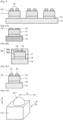
- FIGS. 1 through 7 are cross-sectional views illustrating a micro-light-emitting diode (micro-LED) forming process according to an inventive method of manufacturing a display apparatus.
- micro-LED micro-light-emitting diode
- a semiconductor layer 102 that is to become micro-LEDs which may be referred to as a light-emitting device, is formed on a substrate 101.
- the substrate 101 may be, for example, a sapphire substrate.
- the semiconductor layer 102 may emit light of a certain wavelength as an LED.
- the semiconductor layer 102 may include a GaN-based semiconductor or the like grown on the substrate 101. In this step, the semiconductor layer 102 is not divided into individual micro-LEDs.
- the substrate 101 and the semiconductor layer 102 are collectively referred to as an initial substrate 100.
- the substrate 101 may have, for example, a 4-inch wafer size.
- An electrode may be further formed at a position corresponding to each micro-LED after division on the semiconductor layer 102.
- the electrode is referred to as a light-emitting device-side electrode 12 or device-side electrode 12. Division into micro-LEDs will be described below.
- the device-side electrode 12 is formed at a position corresponding to each micro-LED after division on the semiconductor layer 102. A part of a metal wiring electrically connected to the semiconductor layer 102 may be used as the device-side electrode 12, or a metal pad directly contacting the semiconductor layer 102 may be formed as the device-side electrode 12.
- the device-side electrode 12 may be formed by using at least one of graphene or at least one type of metal selected from a group including, for example, gold (Au), silver (Ag), copper (Cu), aluminum (Al), platinum (Pt), nickel (Ni), chromium (Cr), titanium (Ti), and indium tin oxide (ITO).
- the device-side electrode 12 may include at least one of Au, Ag, or Cu.
- the metal may be used to form an intermetallic compound with a solder alloy which will be described below.
- a relay substrate 112 is bonded by a transfer resin layer 111 to a surface of the initial substrate 100 on which the device-side electrode 12 is formed.
- This process is performed, for example, as follows.
- the transfer resin layer 111 is formed by using spin coating or the like on a surface of the relay substrate 112 facing the initial substrate 100.
- the initial substrate 100 and the relay substrate 112 may be bonded to each other.
- the transfer resin layer 111 may be cured by heat treatment, and thus the initial substrate 100 and the relay substrate 112 may be fixed.
- the transfer resin layer 111 may include a resin material such as polyimide resin, acrylic resin, for example polymethyl methacrylate (PMMA), epoxy resin, polypropylene (PP) resin, polycarbonate resin, or acrylonitrile butadiene styrene (ABS) resin.
- a thermal curing agent is mixed with the resin material.
- any other thermosetting resins may be used as the transfer resin layer 111.
- the transfer resin layer 111 may include a material whose absorbance in a wavelength of laser light used in laser lift-off described below is equal to or greater than 80%.
- the substrate 101 may be separated from the semiconductor layer 102.
- the substrate 101 may be separated by using, for example, laser lift-off.
- laser light of an ultraviolet wavelength is emitted from the substrate 101 to scan an entire surface of the substrate 101. Due to the emission of the laser light, the substrate 101 may be separated from the semiconductor layer 102.
- KrF excimer laser having a wavelength of 248 nm may be used as the laser light.
- the used wavelength is not limited thereto, and may be any wavelength as long as the substrate 101 may be separated from the semiconductor layer 102.
- a source substrate 14 is bonded through a release layer 13 to the semiconductor layer 102.
- the release layer 13 may be a dynamic release layer (DRL).
- DRL dynamic release layer
- this process is performed as follows. First, a resin material that is to become the release layer 13 may be formed on the semiconductor layer 102 by using spin coating or the like. Next, the source substrate 14 may be bonded to the resin material. The resin material is cured by heat treatment to become the release layer 13, and the source substrate 14 may be fixed.
- the source substrate 14 transmits laser light having a wavelength used in a laser ablation process described below.
- a quartz glass substrate may be used as the source substrate 14.
- the quartz glass substrate may have a size that is equal to or greater than that of the substrate 101.
- the source substrate 14, which may be the quartz glass substrate may also have a 4-inch wafer size. A size of the source substrate 14 will be described below.
- the resin material that becomes the release layer 13 may include polyimide resin, acrylic resin for example PMMA, epoxy resin, PP resin, polycarbonate resin, and ABS resin, and the resin material is mixed with a thermal curing agent. Any of other thermosetting resins may be used as the resin material.
- the resin material that becomes the release layer 13 may include a material whose absorbance in a certain wavelength of laser light used in a laser ablation process is equal to or greater than 80%. When the resin material having the absorbance is used, a micro-LED may be easily separated in the laser ablation process.
- a thickness of the release layer 13 may be adjusted during application of the resin material to be equal to or greater than 0.1 ⁇ m and equal to or less than 2 ⁇ m after curing.
- the relay substrate 112 is removed.
- the relay substrate 112 may be removed by using, for example, laser lift-off.
- the relay substrate 112 is removed, for example, as follows.
- Laser light of an ultraviolet wavelength is emitted from the relay substrate 112 to scan an entire surface of the relay substrate 112. Accordingly, due to the emission of the laser light, the transfer resin layer 111 is dissolved, and the relay substrate 112 is separated and removed from a surface of the device-side electrode 12. A portion of the transfer resin layer 111 remaining on the surface of the device-side electrode 12 is removed by using cleaning.
- KrF excimer laser having a wavelength of 248 nm is used as the laser light.
- the used wavelength is not limited thereto, and may be appropriately determined according to a resin material used for the transfer resin layer 111.
- the semiconductor layer 102 may be divided into a plurality of micro-LEDs 11.
- a photoresist may be formed on the semiconductor layer 102 and may be patterned by using photolithography, and the semiconductor layer 102 may be divided into the micro-LEDs 11 through dry etching by using the patterned photoresist as a mask.
- the release layer 13 may also be patterned to have the same shape as the micro-LEDs 11 by using the micro-LEDs 11 as a mask.
- the dry etching process used may be reactive-ion etching (RIE).
- a chip shape of each of the micro-LED 11 on which the device-side electrode 12 is formed may be a rectangular shape in a plan view.
- a length of a longest side from among sides of the rectangular shape of the micro-LED 11 may be equal to or less than, for example, 100 ⁇ m.
- a height of the micro-LED 11, that is, a thickness of the semiconductor layer 102 may be equal to or less than, for example, 500 ⁇ m.
- lower limits of the length, the width, and the height are not particularly limited, and may be any values as long as the micro-LED 11 may be manufactured.
- a gap or interval between the micro-LEDs 11 may be any minimum value as long as the micro-LEDs 11 may be manufactured. Accordingly, an arrangement pitch depends on a size of each micro-LED 11, but may be equal to or less than, for example, 200 ⁇ m. The arrangement pitch may be, for example, a distance between the centers of adjacent micro-LEDs 11 or a distance between edges of adjacent micro-LEDs 11 in the same direction.
- a bump 31 is, in accordance with the invention, formed on each device-side electrode 12.
- the bump 31 may be formed by using any desired method, for example, a ball bump method, a solder paste method, a press method, or a plating method. Also, self-assembly anisotropic conductive paste (SAP) that is anisotropic conductive paste may be used.
- SAP self-assembly anisotropic conductive paste
- a method for forming the bump 31 includes, according to the invention, at least one type of alloy selected from the group including, for example, a Sn-Ag-Cu alloy, a Sn-Bi alloy, a Sn-Bi-Ag alloy, and a Sn-Ag-Cu-Ni alloy.
- the alloys may form an intermetallic compound with a metal of the device-side electrode 12 and a metal of a driving substrate-side electrode, which may also be referred to as a driver-side electrode, and which will be described below.
- a solder alloy that is commercially available may be used as such an alloy.
- a solidus line indicates a temperature line at which a solid material starts to melt
- a liquidus line indicates a temperature line at which a liquid material starts to solidify
- FIGS. 8A through 8C are cross-sectional views for describing a method of forming a bump by using SAP.
- FIGS. 8A through 8C illustrate one micro-LED 11.
- the micro-LED 11 provided after division on the source substrate 14 is prepared. This has already been described as a process up to FIG. 6 .
- the SAP 30 may be applied to a surface on which the device-side electrode 12 is located.
- the SAP 30 includes a thermosetting resin 30a and metal powder 30b such as solder mixed into the thermosetting resin 30a.
- a shape of the metal powder 30b is not limited, and may be any shape such as a particulate shape or a plate shape. The same metal as the solder alloy may be used for the metal powder 30b of the SAP 30.
- the entire source substrate 14 on which the micro-LED 11 is formed may be heated.
- a heating temperature may be, for example, 160°C.
- the disclosure is not limited thereto. Due to the heating, the metal powder 30b may aggregate on a metal surface of the device-side electrode 12. A resin component in the SAP 30 is dissolved and removed. Accordingly, as shown in FIG. 8C , the metal powder 30b aggregating on the metal surface of the device-side electrode 12 may become the bump 31.
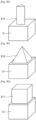
- FIGS. 9A through 9I are perspective views illustrating a shape of the bump 31.
- the bump 31 may have a dome shape 311.
- the bump 31 may have an arch shape 312.
- the bump 31 may have circular cylindrical shape 313.
- the bump 31 may have a semi-circular cylindrical shape 314.
- the bump 31 may have a semi-elliptical cylindrical shape 315.
- the bump 31 may have a semi-m-angular cylindrical shape 318, where the term 'semi-m angular cylindrical shape' may refer to a shape having at least one side whose length is different from others, and m is an integer equal to or greater than 4.
- the bump 31 may have an irregular shape 319.
- An area of the bump 31 is not limited by its shape, and an area of a bottom surface of the bump 31 may be less than an area of the device-side electrode 12 as shown in FIG. 9A or may be almost the same as an area of the device-side electrode 12 as shown in FIG. 9B .
- a size of the bump 31 may vary according to an area of the device-side electrode 12 and a driver-side electrode which will be described below.
- a thickness T of the metal layer is, according to the invention claimed, equal to or less than half of the length A of the short side. Because the metal layer has a thickness in this range, when the device-side electrode 12 and the driver-side electrode are connected to each other, a metal may be prevented from overflowing around and contacting other wirings or pads. Accordingly, a size of the bump 31 may be designed in consideration of the thickness T of the metal layer when the display apparatus is completed.
- a height t of the bump 31 may be equal to or greater than 2 ⁇ m and equal to or less than 20 ⁇ m.
- a size of the bump 31 is not limited, and may appropriately vary according to a size of the device-side electrode 12, a shape of the bump 31, and the like.
- the height t of the bump 31 may indicate a distance from a surface of the device-side electrode to a highest portion of the bump 31, as shown in FIG. 9A .
- the height t of the bump 31 may also apply to the bump 31 of each of FIGS. 9B through 9I .
- Example Method 1 in the process so far, a source substrate structure in which the micro-LED 11 is held to the source substrate 14 by the release layer 13 may be provided.
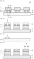
- FIG. 10 is a cross-sectional view illustrating a driving substrate according to a method of manufacturing a display apparatus.
- a driving substrate 20 may have a size corresponding to a size of the manufactured display apparatus. A size of the driving substrate 20 will be described below.
- the driving substrate 20 may include an electrode to be connected to the device-side electrode 12, along with a thin-film transistor (TFT) or a wiring needed to supply power to the micro-LED 11.
- TFT thin-film transistor
- an electrode provided on the driving substrate 20 may be referred to as a driving substrate-side electrode 21 or a driver-side electrode 21.
- a part of a metal wiring formed on the driving substrate 20 may be used as the driver-side electrode 21, or a metal pad connected to a wiring may be formed as the driver-side electrode 21.
- the same metal as that of the device-side electrode 12 may be used for the driver-side electrode 21.
- an adhesive layer 32 may, according to one of two options of the invention as claimed, be formed on a surface of the driving substrate 20 on which the driver-side electrode 21 is formed.
- a non-conductive adhesive such as non-conductive film (NCF), non-conductive paste (NCP), or non-conductive adhesive (NCA) may be used for the adhesive layer 32.
- a mixture of a thermal curing agent with, for example, epoxy resin, acrylic resin, polyamide resin, polyacrylamide resin, polyvinyl alcohol, or polyvinylpyrrolidone may be used for the adhesive layer 32.
- the adhesive layer 32 is not limited thereto, and a thermosetting resin may be used for the adhesive layer 32.
- a photoresist for example a positive photoresist, may be used for the adhesive layer 32.
- the adhesive layer 32 may be applied to an entire surface of the driving substrate 20 on which the driver-side electrode 21 is formed by using, for example, a laminating method or a printing method.
- a thickness of the adhesive layer 32 has a range equal to or greater than 1 ⁇ m and equal to or less than 50 ⁇ m.
- a pressing and heating process may be used.
- the bump 31 formed on the device-side electrode 12 may reach the driver-side electrode 21 in the pressing and heating process.
- Example Method 1 in the process so far, a driving substrate structure on which the adhesive layer 32 exists may be provided.
- FIGS. 11 and 12 are cross-sectional views for describing a method of connecting the micro-LED 11 and the driving substrate 20 according to a method of manufacturing a display apparatus.
- the micro-LED 11 and the driving substrate 20 are connected by using laser ablation. As shown in FIG. 11 , first, a position of the source substrate 14 at which one micro-LED 11 is to be connected to the driving substrate 20 may be determined. In this case, a position at which a device-side pad of the one micro-LED 11 is connectable to the corresponding driver-side electrode 21 for driving the one micro-LED 11 may be determined as the position.
- laser light 16 having a certain wavelength is emitted to the one micro-LED 11 from the source substrate 14. Due to the emission of the laser light 16, the release layer 13 that adheres the one micro-LED 11 to the source substrate 14 may be dissolved and the one micro-LED 11 may be released to the driving substrate 20. The released micro-LED 11 is caught by the adhesive layer 32 on the driving substrate 20.
- KrF excimer laser having a wavelength of 248 nm may be used as the laser light 16.
- YAG(FHG) laser having a wavelength of 266 nm or YAG(THG) laser having a wavelength of 355 nm may be used.
- laser having a wavelength of 355 nm may be used for a glass substrate instead of a quartz glass substrate, and may have different member and device costs. Laser light of other wavelengths may also be used.
- a beam diameter of the laser light 16 may be equal to or greater than a chip size of the one micro-LED 11. However, in embodiments a beam diameter of the laser light 16 may be a size that does not affect an adjacent micro-LED 11 on the source substrate 14. Because the laser light 16 has such a beam diameter, the micro-LEDs 11 that are parallel on the source substrate 14 may be selectively transferred one by one to the driving substrate 20.
- One beam of the laser light 16 may be emitted, or a plurality of beams may be simultaneously emitted at desired pitches by using a mask or the like or preparing a plurality of laser light sources. In the latter case, multiple micro-LEDs 11 may be simultaneously transferred.
- a gap between the driving substrate 20 and the micro-LED 11 when a laser ablation process is performed may have a range equal to or greater than 1 ⁇ m and equal to or less than 200 ⁇ m. Because the gap is equal to or greater than 1 ⁇ m and equal to or less than 200 ⁇ m,the micro-LED 11 separated by the laser ablation process may be caught by the driving substrate 20 at a target position.
- a heating temperature may be a temperature at which the bump 31 is dissolved.
- the bump 31 is formed by using ECO solder that is a product of Senju Metal Industry Co., Ltd., a same temperature as a solder reflow temperature is used as the heating temperature.
- a melting temperature of the ECO solder varies according to a composition and is equal to or higher than 139°C and equal to or lower than 245°C. Accordingly, the heating temperature in the pressing and heating process is set according to a used solder alloy, for example ECO solder.
- the heating temperature may be a temperature at which the adhesive layer 32 is cured.
- the adhesive layer 32 depends on a pressing force when NCF, NCP, or NCA including a thermosetting resin is used, when a pressure is equal to or greater than 1 MPa and equal to or less than 10 MPa, a curing temperature may be equal to or higher than 100°C and equal to or lower than 200°C. This temperature range overlaps a range of the above-described solder reflow temperature. Accordingly, a temperature in the pressing and heating process may be appropriately determined according to characteristics of a curing temperature of a resin material of the adhesive layer 32 and a composition of a solder alloy of the bump 31.
- a display apparatus 10 is completed.
- the device-side electrode 12 and the driver-side electrode 21 are connected to each other when the bump 31 becomes a metal layer 35.
- the metal layer 35 is an intermetallic compound formed of a metal of the bump 31 and a metal of each electrode.
- the thickness T of the metal layer 35 has already been described.
- the intermetallic compound is a compound formed of two or more types of metals.
- the intermetallic compound is a type of alloy.
- a general alloy has a solid solution structure in which a structure of an original metal is maintained and atoms of another metal are randomly substituted.
- a general alloy is referred to as a solid solution alloy.
- a solid solution alloy may be formed to have various composition ratios to some extent although constituent metals are the same.
- An intermetallic compound is a compound having a crystal structure different from that of an original metal.
- a composition ratio of an intermetallic compound may be a simple integer ratio, for example 1:2 or 1:3, of two or more types of metals.
- Such an intermetallic compound may be formed when a metal of the bump 31 is bonded to a metal of each of the device-side electrode 12 and the driver-side electrode 21. Accordingly, the intermetallic compound may be formed at a position including at least one of an interface 12a between the device-side electrode 12 and the metal layer 35 or an interface 21a between the driver-side electrode 21 and the metal layer 35.
- a process of connecting the micro-LED 11 and the driving substrate 20 and then connecting or wiring a necessary peripheral circuit is performed as a method of manufacturing the display apparatus 10.
- Example Method 1 may have the following effects.
- Example Method 1 in the completed display apparatus 10, the micro-LED 11 is connected by the metal layer 35 and a thin film of the adhesive layer 32 to the driving substrate 20 that is flat. Accordingly, in Example Method 1, because the driving substrate 20 or the source substrate 14 onto which the micro-LED 11 is held has no stepped portion other than a device structure or an electrode, the micro-LED 11 and the driving substrate 20 may be easily and reliably connected to each other when compared to related art methods. Also, in Example Method 1, because the driving substrate 20 and the micro-LED 11 are connected to each other by a two-layer structure including the metal layer 35 and the adhesive layer 32, the driving substrate 20 and the micro-LED 11 may be firmly connected to each other.
- Example Method 1 because the micro-LED 11 and the driving substrate 20 are connected to each other by the metal layer 35 formed an intermetallic compound, electrical conductivity is high.
- the bump 31 is formed on the device-side electrode 12 in a state where the micro-LED 11 is held onto the source substrate 14.
- the source substrate 14 onto which the micro-LED 11 is held may have a wafer size.
- the driving substrate 20 may have a display size.
- Table 3 and Table 4 show arrangement pitches and sizes of the source substrate 14 and the driving substrate 20, and a ratio between the source substrate 14 and the driving substrate 20 for each panel size according to various embodiments.
- Table 3 is for an embodiment including a 32-inch panel
- Table 4 is for an embodiment including a 88-inch panel
- Table 5 is for an embodiment including a 100-inch panel.
- a chip size of the micro-LED 11 is 40 ⁇ m X 40 ⁇ m
- a resolution of a display panel is 4K
- the number of pixels is 3,840 X 2,160.
- a ratio between arrangement pitches of the source substrate 14 and the driving substrate 20 is 10 times, and a ratio between areas of the source substrate 14 and the driving substrate 20 is about 440 times.
- a ratio between arrangement pitches of the source substrate 14 and the driving substrate 20 is 12 times, and a ratio between areas of the source substrate 14 and the driving substrate 20 is about 569 times.
- an arrangement pitch of the micro-LEDs 11 on the driving substrate 20 may be at least 3 times an arrangement pitch of the micro-LEDs 11 on the source substrate 14. Also, as a panel size increases, a ratio of arrangement pitches increases. Also, an upper limit of an arrangement pitch on the driving substrate 20 may be any value as long as a desired number of micro-LEDs 11 may be arranged on a display panel.
- a ratio of areas may range from about 57 times to about 569 times, and as a panel size increases, a ratio of areas increases. Accordingly, the bump 31 is formed by applying the SAP 30, an application area when the SAP 30 is applied to the source substrate is less than an application area when the SAP 30 is applied the driving substrate 20.
- the number of micro-LEDs held to the source substrate 14 is about 1.88 million. Accordingly, about 4.4 source substrates 14 are required at a resolution of 4 K, or about 8.3 million pixels.
- the SAP 30 when the SAP 30 is coated, application coated area of a required number of source substrates 14 relative to an area of the driving substrate 20 is about 1/13 in a 32-inch panel, about 1/100 in an 88-inch panel, and about 1/144 in a 100-inch panel. Accordingly, in Example Method 1, the amount of used SAP 30 may be reduced. Accordingly, manufacturing costs or costs in a coating process may be reduced. Also, because arrangement pitches of the micro-LEDs 11 are greatly different, when the SAP 30 is applied to the source substrate 14, the amount of unnecessary SAP may also be reduced.
- Example Method 1 when the micro-LED 11 is transferred from the source substrate 14 to the driving substrate 20, there is a difference of 3 times or more in an arrangement pitch ratio and there is a difference of 10 times or more in an application area ratio, according to a size of a display panel. Accordingly, for example, when compared to a method of forming the adhesive layer 32 along with the bump 31 on the driving substrate 20, in Example Method 1, a manufacturing process may be simplified and a waste of materials may be reduced.
- Example Method 1 because a metal for easily forming an intermetallic compound such as a solder alloy is used for the bump 31 as described above, an intermetallic compound is easily formed with metals used for the device-side electrode 12 and the driver-side electrode 21.
- an intermetallic compound is more easily formed than an AuSn alloy or the like formed on an electrode surface by using a plating method.
- Example Method 1 because the bump 31 is formed by using the SAP 30, the bump 31 may be reliably formed even on an electrode having a micro-structure.
- Example Method 1 because the bump 31 is formed by using the SAP 30, a process time is shorter than that of a method of forming the bump 31 by fixing a ball obtained by dissolving a front end portion of a metal wire or by performing a needle dispensing or photoresist process.
- Example Method 2 according to the invention is different from Example Method 1 in a process of connecting the micro-LED 11 and the driving substrate 20.
- Other manufacturing processes are the same as those in Example Method 1.
- elements having the same functions as those of Example Method 1 are denoted by the same reference numerals even when arrangements are different.
- FIG. 13 is a cross-sectional view of the source substrate 14 on which the micro-LED 11 is held before the micro-LED 11 is connected to the driving substrate 20 in Example Method 2.
- FIG. 14 is a cross-sectional view of the driving substrate 20 before the micro-LED 11 is connected to the driving substrate 20 in Example Method 2.
- the bump 31 is formed on the device-side electrode 12 of the micro-LED 11 provided after division on the source substrate 14, and the adhesive layer 32 is, according to the other of two options of the invention as claimed, formed to cover the bump 31 of each micro-LED 11.
- a method of forming the bump 31 and a metal material of the bump 31 are the same as those in Example Method 1.
- the adhesive layer 32 is formed by using, for example, a printing method, and is divided to correspond to each micro-LED 11.
- a thickness of the adhesive layer 32 including the bump 31 is, in accordance with the invention as claimed, equal to or less than 50 ⁇ m. In embodiments, a lower limit of a thickness of the adhesive layer 32 is determined so that the adhesive layer 32 covers the bump 31.
- a thickness of the adhesive layer 32 may have a range equal to or greater than 3 ⁇ m and equal to or less than 21 ⁇ m.
- Example Method 2 a source substrate structure in which the adhesive layer 32 is located over the bump 31 is provided.
- the driver-side electrode 21 is formed on the driving substrate 20. Accordingly, in Example Method 2, the adhesive layer 32 is not formed on the driving substrate 20, unlike in Example Method 1.
- the device-side electrode 12 and the driver-side electrode 21 are connected to each other by the metal layer 35, and the whole or a part of the metal layer 35 is formed of an intermetallic compound. Also, portions of the micro-LED 11 and the driving substrate 20 other than electrodes are connected to each other by the adhesive layer 32.
- Example Method 2 has the following effect in addition to the same effect as that of Example Method 1.
- Example Method 2 the adhesive layer 32 is formed on the micro-LED 11 of the source substrate 14. Accordingly, Example Method 2 may reduce an application area of the adhesive layer 32 and may further reduce material costs when compared to Example Method 1.
- Example Method 2 may simplify a manufacturing process and may reduce a waste of materials, when compared to, for example, a method of forming both the bump 31 and the adhesive layer 32 on the driving substrate 20.
- Example Method 3 falling outside the scope of the claimed invention is different from Example Methods 1 and 2 in a process of connecting the micro-LED 11 and the driving substrate 20.
- Other processes are the same as those in Example Method 1.
- elements having the same functions as those in Example Method 1 are denoted by the same reference numerals even when arrangements are different.
- FIG. 15 is a cross-sectional view of the source substrate 14 on which the micro-LED 11 is held before the micro-LED 11 is connected to the driving substrate 20 in Example Method 3.
- Example Method 3 as shown in FIG. 15 , the SAP 30 is applied to each divided micro-LED 11.
- a layer formed by coating the SAP 30 is a resin layer including the thermosetting resin 30a and the metal powder 30b mixed into the thermosetting resin 30a.
- the resin layer is referred to as an SAP layer 36.
- the SAP 30 of Example Method 1 is used for the SAP layer 36 of Example Method 3.
- the SAP layer 36 is formed only on a surface of the micro-LED 11 on which the device-side electrode 12 is provided, by using, for example, a printing method. Accordingly, the SAP layer 36 is divided to correspond to each micro-LED 11.
- a thickness of the SAP layer 36 is equal to or less than, for example, 50 ⁇ m.
- a thickness of the metal layer 35 described with reference to Example Method 1 may be applied.
- Example Method 3 a source substrate structure in which the SAP layer 36 is located is provided.
- the adhesive layer 32 is not formed on the driving substrate 20, like in Example Method 2 as shown for example in FIG. 14 .
- Example Method 3 in a pressing and heating process, the metal powder 30b in the SAP 30 aggregates between electrodes to form the metal layer 35 that connects the electrodes to each other.
- the device-side electrode 12 and the driver-side electrode 21 are connected to each other by the metal layer 35, and the whole or a part of the metal layer 35 is formed of an intermetallic compound. Also, portions of the micro-LED 11 and the driving substrate 20 other than electrodes are connected to each other by the adhesive layer 32.
- Example Method 3 has the following effect in addition to the same effect as that of Example Method 1.
- Example Method 3 may simplify a manufacturing process when compared to Example Methods 1 and 2.
- Example Method 3 may reduce a waste of SAP materials when compared to, for example, a method of applying SAP to an entire surface of the driving substrate 20.
- Example Method 3 may use anisotropic conductive paste (ACP) or an anisotropic conductive film (ACF), instead of the SAP 30.
- ACP anisotropic conductive paste
- ACF anisotropic conductive film
- FIG. 16 is a cross-sectional view of the source substrate 14 on which the micro-LED 11 is held before the micro-LED 11 is connected to the driving substrate 20 in Modification of Example Method 3.
- the adhesive layer 32 is further provided on the SAP layer 36 of Example Method 3.
- the adhesive layer 32 on the SAP layer 36 is divided to correspond to each micro-LED 11, like the SAP layer 36.
- the SAP 30 has the thermosetting resin 30a
- the SAP 30 may have a small adhesive force depending on a resin component. Accordingly, depending on a resin component of the used SAP 30, the micro-LEDs 11 separated by a laser ablation process may not be caught, or may not be properly adhered, by the driving substrate 20 in some instances.
- the micro-LED 11 may be caught by the driving substrate 20 at a target position in a laser ablation process, without depending on a resin component of the used SAP 30.
- a total thickness of the SAP layer 36 and the adhesive layer 32 may have a range equal to or greater than 6 ⁇ m and equal to or less than 100 ⁇ m. This is to form the adhesive layer 32 on the SAP layer 36 to a thickness equal to or greater than 1 ⁇ m and equal to or less than 50 ⁇ m,when a thickness of the SAP layer 36 is equal to or greater than 5 ⁇ m and equal to or less than 50 ⁇ m. Such thicknesses may be appropriately changed.
- a process of connecting the micro-LED 11 and the driving substrate 20 in Modification of Example Method 3 may be the same as that in Example Method 3.
- Modification of Example Method 3 may have the effect of reliably catching the micro-LED 11 by providing the adhesive layer 32, in addition to the same effect as that of Example Method 3.
- Example Method 4 is different from Example Methods 1 through 3 in a process of connecting the micro-LED 11 and the driving substrate 20.
- Other manufacturing processes are the same as those in Example Method 1.
- elements having the same functions as those in Example Method 1 are denoted by the same reference numerals even when arrangements are different.
- FIG. 17 is a cross-sectional view of the source substrate 14 on which the micro-LED 11 is held before the micro-LED 11 is connected to the driving substrate 20 in Example Method 4.
- FIG. 18 is a cross-sectional view of the driving substrate 20 before the driving substrate 20 is connected to the micro-LED 11 in Example Method 4.
- the adhesive layer 32 is formed on a surface of the micro-LED 11 on which the device-side electrode 12 is provided.
- the bump 31 is not formed, unlike in inventive Example Methods 1 and 2.
- the adhesive layer 32 is formed only on a surface of the micro-LED 11 on which the device-side electrode 12 is located, by using, for example, a printing method. Accordingly, the adhesive layer 32 is divided to correspond to each micro-LED 11. The same material as that of Example Method 1 is used for the adhesive layer 32.
- Example Method 4 a source substrate structure in which the adhesive layer 32 is located on the device-side electrode 12 is provided.
- a bump 38 is formed on the driver-side electrode 21 of the driving substrate 20, as shown in FIG. 18 .
- a method of forming the bump 38 may be the same as a method of forming a bump on the device-side electrode 12 of Example Method 1.
- Example Method 4 a driving substrate structure in which the bump 38 is located on the driver-side electrode 21 is provided.
- the device-side electrode 12 and the driver-side electrode 21 are connected to each other by the metal layer 35, and the whole or a part of the metal layer 35 is formed of an intermetallic compound. Also, portions of the micro-LED 11 and the driving substrate 20 other than electrodes are connected to each other by the adhesive layer 32.
- Example Method 4 has the following effect in addition to the same effect as that of Example Method 1.
- Example Method 4 the adhesive layer 32 is formed on the micro-LED 11 of the source substrate 14, and the bump 31 is formed on the driving substrate 20. Accordingly, Example Method 4 may reduce an application area of the adhesive layer 32 and may reduce manufacturing costs of the adhesive layer 32 when compared to Example Method 1.
- Example Method 4 may simplify a manufacturing process and may reduce a waste of materials, when compared to, for example, a method of forming both the adhesive layer 32 and the bump 31 on the driving substrate 20.
- Example 1 first, the device-side electrode 12 and a semiconductor layer 102 that is to become an LED were formed on the substrate 101 that is a sapphire substrate having a 4-inch size.
- the device-side electrode 12 was a gold (Au) pad directly formed on the semiconductor layer 102.
- a thickness of the semiconductor layer 102 was 5 ⁇ m, and the device-side electrode 12 (pad) had a rectangular shape of 60 ⁇ m X 35 ⁇ m.
- a polyimide resin mixed with a thermal curing agent was applied by using spin coating to the relay substrate 112 to a thickness of 10 ⁇ m, to form the transfer resin layer 111.
- a quartz glass substrate was used as the relay substrate 112.
- the substrate 101 that is a sapphire substrate and the relay substrate 112 were superimposed so that the semiconductor layer 102 and the transfer resin layer 111 contacted each other, and were pressed and heated at 1000 N and 250°C for 10 minutes to bond the substrate 101 and the relay substrate 112.
- KrF excimer laser having a wavelength of 248 nm was emitted from the substrate 101 that is a sapphire substrate at an energy density of 200 mJ/cm 2 , to separate the semiconductor layer 102 from the substrate 101.
- a quartz glass substrate was prepared as the source substrate 14, a resin layer having a thickness of 0.15 ⁇ m was formed by spin coating a polyimide resin mixed with a thermal curing agent on the source substrate 14, and the release layer 13 was formed by firing the resin layer in a vacuum oven at 250°C for 1 hour.
- a substance obtained by diluting HD3007 (HD Microsystems) to desired solid content was used as the polyimide resin.
- An absorbance of the HD3007 for ultraviolet light of a wavelength of 248 nm is equal to or greater than 99%.
- a surface of the semiconductor layer 102 on the relay substrate 112 was superimposed on the release layer 13 of the source substrate 14, and was pressed and heated by using a bonding device at 1000 N and 250°C for 10 minutes, to bond the source substrate 14 and the relay substrate 112.
- KrF excimer laser having a wavelength of 248 nm was emitted from the relay substrate 112 at an energy density of 200 mJ/cm 2 , to separate the transfer resin layer 111 from the relay substrate 112.
- NMP N-methyl-pyrrolidone
- the semiconductor layer 102 was divided into the micro-LEDs 11 by using dry etching (oxygen plasma RIE).
- the SAP 30 was applied by using a dispenser to an entire surface of the source substrate 14 including the micro-LED 11. After the SAP 30 was applied, the SAP 30 was heated by using a hot plate to 160°C for 1 minute, and then was cooled to room temperature. Reflow self-assembly anisotropic conductive paste Epowell AP series (Sekisui Chemical Co., Ltd.) was used as the SAP 30.
- a metal in the SAP 30 is a SnBi and SnAgCu solder alloy, and a resin is a thermosetting thermoplastic epoxy resin.
- N-methyl pyrrolidone was sprayed to a resin component of the SAP 30, a solvent component was rinsed off by using isopropanol, and vacuum drying was performed under reduced pressure. Accordingly, the bump 31 having a height of 3 ⁇ m was formed on the device-side electrode 12.
- Comparative Example 1 the bump 31 is not formed on the micro-LED 11. Comparative Example 1 is the same as Example 1 except that the bump 31 is not formed.
- a glass substrate on which copper (Cu) comb electrodes were wired at regular intervals was prepared.
- the glass substrate corresponds to the driving substrate 20.
- the comb electrodes correspond to the driver-side electrodes 21.
- a size of each of the comb electrodes is 25 ⁇ m X 70 ⁇ m.
- the adhesive layer 32 was formed by applying a non-conductive material to an entire surface of the glass substrate including the copper comb electrode by using an applicator to a thickness of 30 ⁇ m.
- the non-conductive material is a thermosetting resin having a bisphenol A liquid epoxy resin as a main component.
- a surface of the source substrate 14 onto which the micro-LED 11 was held and a surface of the glass substrate on which the comb electrode was formed were held to face each other with a certain gap therebetween.
- the micro-LED 11 was transferred to the glass substrate during a laser ablation process.
- the source substrate 14 and the glass substrate were held so that a gap between closest portions of the source substrate 14 and the glass substrate was 100 ⁇ m.
- the laser ablation process was performed by using KrF excimer laser having a wavelength of 248 nm at irradiation energy of 100 mJ/cm 2 .
- Example 1 a pressing and heating process was not performed after the laser ablation process for evaluation test.
- a position of the micro-LED 11 caught in the glass substrate during the laser ablation process was measured.
- an interval between an edge of a target comb electrode and an edge of the micro-LED 11 was measured.
- the number of samples to be measured that is the number of the micro-LEDs 11 is 30 in both Example 1 and Comparative Example 1.
- Example 1 In Example 1 (with the bump 31), a maximum value of mismatch of measured values was ⁇ 2 ⁇ m. In Comparative Example 1 (with no bump 31), a maximum value of mismatch of measured values was ⁇ 5 ⁇ m.
- Example 1 where the bump 31 was formed on the micro-LED 11 has less positional deviation during transfer than Comparative Example 1 where there was no bump 31.
- a thermosetting resin used for the adhesive layer 32 is the same as that described above.
- KrF excimer laser having a wavelength of 248 nm was used, and laser light was emitted at irradiation energy of each of 50 mJ/ cm 2 , 60 mJ/cm 2 , 70 mJ/cm 2 , 80 mJ/cm 2 , 90 mJ/cm 2 , and 100 mJ/cm 2 for each glass substrate sample to transfer the micro-LED 11.
- the transfer position accuracy was evaluated for each glass substrate sample and each irradiation energy.
- a result is shown in Table 6. Also, an evaluation result was obtained by evaluating the amount of deviation from a target position, and representing the amount of deviation equal to or greater than ⁇ 10 ⁇ m by using X, the amount of deviation equal to or greater than ⁇ 2 ⁇ m and equal to or less than 10 ⁇ m by using ⁇ , and the amount of deviation less than ⁇ 2 ⁇ m by using O.
- Example 1 (with the bump 31) has high position accuracy even though irradiation energy is low, when compared to Comparative Example 1 (with no bump 31). Accordingly, it is found that an irradiation energy margin is large when the bump 31 is formed. When it comes to a thickness of a non-conductive material, even when Example 1 (with the bump 31) has a lower thickness than that of Comparative Example 1 (with no bump 31), Example 1 has less positional deviation than Comparative Example 1. Accordingly, it is found that a thickness margin during application of a non-conductive material is large when the bump 31 is formed. Also, because a film thickness of a non-conductive material may be reduced when the bump 31 is formed, the amount of non-conductive material used may be reduced and costs may be reduced.
- Example 2 the micro-LED 11 was formed on the source substrate 14 and the bump 31 was formed on an electrode of the micro-LED 11, like in Example 1.
- Example 2 the adhesive layer 32 was formed on the bump 31 by applying a non-conductive material having a bisphenol A liquid epoxy resin as a main component to an entire surface of the source substrate 14 by using an applicator to a thickness of 10 ⁇ m.
- a glass substrate on which copper (Cu) comb electrodes were wired at constant intervals was prepared.
- a size of each of the comb electrodes is 25 ⁇ m X 70 ⁇ m.
- a surface of the source substrate 14 onto which the micro-LED 11 was held and a surface of the glass substrate on which the comb electrode was formed were held to face each other, and the micro-LED 11 was transferred to the glass substrate during a laser ablation process.
- the source substrate 14 and the glass substrate were held so that a gap between closest portions of the source substrate 14 and the glass substrate was 100 ⁇ m.
- the laser ablation process was performed by using KrF excimer laser having a wavelength of 248 nm at irradiation energy of 100 mJ/cm 2 .
- Example 2 Even in Example 2, a pressing and heating process was not performed after the laser ablation process for evaluation test, like in Example 1.
- a position of the micro-LED 11 caught by the glass substrate during the laser ablation process was measured.
- an interval between an edge of a target comb electrode and an edge of the micro-LED 11 was measured.
- the number of samples to be measured that is the number of the micro-LEDs 11 is 30 in both Example 2 and Comparative Example 1.
- Example 2 (with the bump 31), a maximum value of mismatch of measured values was ⁇ 2 ⁇ m.
- Comparative Example 1 a maximum value of mismatch of measured values was ⁇ 5 ⁇ m.
- Example 2 where the bump 31 was formed on the micro-LED 11 and then the adhesive layer 32 was further applied has less positional deviation during transfer than Comparative Example 1 where there was no bump 31.
- KrF excimer laser having a wavelength of 248 nm was used, and laser light was emitted at irradiation energy of each of 50, 60, 70, 80, 90, and 100 mJ/cm 2 for each glass substrate sample to transfer the micro-LED 11.
- Transfer position accuracy was evaluated for each glass substrate sample and each irradiation energy. A result is shown in Table 7. Also, an evaluation result was obtained by representing the amount of deviation equal to or greater than ⁇ 10 ⁇ m by using X, the amount of deviation equal to or greater than ⁇ 2 ⁇ m and equal to or less than 10 ⁇ m by using ⁇ , and the amount of deviation less than ⁇ 2 ⁇ m by using O, like in Table 6.
- Example 2 (with the bump 31) has high position accuracy even though irradiation energy is low, when compared to Comparative Example 1 (with no bump 31). Accordingly, it is found that an irradiation energy margin is large when the bump 31 is formed.
- Film Thickness 30 ⁇ m Irradiation Energy (mJ/cm 2 ) 50 60 70 80 90 100
- Example 2 ⁇ ⁇ ⁇ ⁇ ⁇ Comparative Example 1 X X ⁇ ⁇ ⁇ ⁇ ⁇
- embodiments of the disclosure may have high transfer position accuracy of the micro-LED 11 to the driving substrate 20. Also, embodiments of the disclosure may have a large irradiation energy margin. Accordingly, it is found that a method of manufacturing the display apparatus 10 of the micro-LED 11 according to the disclosure may be simpler than that of the prior art, thereby improving yield.
- a metal for easily forming an intermetallic compound is used as a metal for connecting the device-side electrode 12 and the driver-side electrode 21.
- the disclosure is not limited to a metal for easily forming an intermetallic compound.
- a metal for electrically connecting the device-side electrode 12 and the driver-side electrode 21 may be used.
- the device-side electrode 12 and the driver-side electrode 21 are connected to each other by the metal layer 35, and the micro-LED 11 and the driving substrate 20 are connected to each other by the adhesive layer 32. Accordingly, even in this case, the micro-LED 11 and the driving substrate 20 are connected to each other by a two-layer structure including the metal layer 35 and the adhesive layer 32.
- a manufacturing method when a metal for easily forming an intermetallic compound is not used is the same as that in some embodiments, and thus the micro-LED 11 and the driving substrate 20 may be easily and reliably connected to each other.
- a light-emitting device-side electrode and a driving substrate-side electrode are connected to each other by a metal layer on which an intermetallic compound is formed, a light-emitting device and a driving substrate for driving the light-emitting device may be easily and reliably bonded to each other.
- the light-emitting device-side electrode and the driving substrate-side electrode are connected to each other by the metal layer and the light-emitting device and the driving substrate are connected to each other by an adhesive layer, the light-emitting device and the driving substrate for driving the light-emitting device may be easily and reliably bonded to each other.
Landscapes
- Devices For Indicating Variable Information By Combining Individual Elements (AREA)
- Led Device Packages (AREA)
Claims (5)
- Procédé de fabrication d'un appareil d'affichage (10), le procédé comprenant :la formation d'une couche semi-conductrice (102) sur un substrat de saphir (101) ;la formation d'une électrode côté dispositif (12) sur la couche semi-conductrice ;le transfert de la couche semi-conductrice sur un substrat de relais (112) par adhérence du substrat de relais sur une surface de l'électrode côté dispositif ;le retrait du substrat de saphir de la couche semi-conductrice ;la formation d'une couche de décollement (13) comprenant un matériau de résine sur un substrat source (14) conçu pour transmettre de la lumière laser d'une longueur d'onde prédéfinie ;le transfert de la couche semi-conductrice formée sur le substrat de relais vers la couche de décollement ;le retrait du substrat de relais ;la formation d'un dispositif électroluminescent (11) par division de la couche semi-conductrice ;la formation d'une bosse (31) sur l'électrode côté dispositif ;la formation d'une couche adhésive (32) sur le substrat conducteur sur lequel une électrode côté conducteur est formée ou sur le dispositif électroluminescent comprenant l'électrode côté dispositif et la bosse ; etl'émission de la lumière laser de la longueur prédéfinie vers le dispositif électroluminescent pour séparer le dispositif électroluminescent de la couche de décollement et faire adhérer le dispositif électroluminescent sur un substrat conducteur ; etladite bosse étant constituée d'une couche métallique qui comprend au moins un type d'alliage parmi un alliage Sn-Ag-Cu, un alliage Sn-Bi, un alliage Sn-Bi-Ag, et un alliage Sn-Ag-Cu-Ni, l'épaisseur de la couche métallique étant inférieure ou égale à la moitié de la longueur du côté le plus court de l'électrode côté dispositif, et l'épaisseur de la couche adhésive comportant une plage allant de 1 µm à 50 µm.
- Procédé selon la revendication 1, ledit dispositif électroluminescent (11) étant compris dans une pluralité de dispositifs électroluminescents formés par la division, et
ladite pluralité de dispositifs électroluminescents étant fixée au substrat source (14) par la couche de décollement (13). - Procédé selon la revendication 1, ledit dispositif électroluminescent comportant une forme rectangulaire,la longueur du côté le plus long du dispositif électroluminescent étant inférieure ou égale à 100 µm,ledit dispositif électroluminescent étant compris dans une pluralité de dispositifs électroluminescents formés par la division, etle pas d'agencement de la pluralité de dispositifs électroluminescents sur le substrat source étant inférieur ou égal à 200 µm.
- Procédé selon la revendication 1, ledit dispositif électroluminescent étant compris dans une pluralité de dispositifs électroluminescents formés par la division, etune partie de la pluralité de dispositifs électroluminescents adhérant au substrat conducteur selon la taille du panneau d'affichage,le pas d'agencement de la partie de la pluralité de dispositifs électroluminescents sur le substrat conducteur étant au moins 3 fois plus grande que le pas d'agencement de la pluralité de dispositifs électroluminescents sur le substrat source.
- Procédé selon la revendication 1, chacune parmi l'électrode côté dispositif (13) et une électrode côté conducteur (21) formée sur le substrat conducteur comprenant au moins un élément parmi le graphène, l'or (Au), l'argent (Ag), le cuivre (Cu), l'aluminium (Al), le platine (Pt), le nickel (Ni), le chrome (Cr), le titane (Ti) et l'oxyde d'étain et d'indium (ITO).
Applications Claiming Priority (3)
| Application Number | Priority Date | Filing Date | Title |
|---|---|---|---|
| JP2019099645A JP2020194886A (ja) | 2019-05-28 | 2019-05-28 | ディスプレイ装置、ソース基板構造体、駆動基板構造体、およびディスプレイ装置の製造方法 |
| KR1020200006751A KR102933975B1 (ko) | 2019-05-28 | 2020-01-17 | 디스플레이 장치, 소스 기판 구조체, 구동 기판 구조체, 및 디스플레이 장치의 제조 방법 |
| PCT/KR2020/005121 WO2020242053A1 (fr) | 2019-05-28 | 2020-04-16 | Appareil d'affichage, structure de substrat source, structure de substrat de commande et procédé de fabrication d'appareil d'affichage |
Publications (3)
| Publication Number | Publication Date |
|---|---|
| EP3844818A1 EP3844818A1 (fr) | 2021-07-07 |
| EP3844818A4 EP3844818A4 (fr) | 2021-12-01 |
| EP3844818B1 true EP3844818B1 (fr) | 2023-09-06 |
Family
ID=73546032
Family Applications (1)
| Application Number | Title | Priority Date | Filing Date |
|---|---|---|---|
| EP20814013.7A Active EP3844818B1 (fr) | 2019-05-28 | 2020-04-16 | Procédé de fabrication d'appareil d'affichage |
Country Status (3)
| Country | Link |
|---|---|
| EP (1) | EP3844818B1 (fr) |
| JP (1) | JP2020194886A (fr) |
| KR (1) | KR102933975B1 (fr) |
Families Citing this family (9)
| Publication number | Priority date | Publication date | Assignee | Title |
|---|---|---|---|---|
| CN114141716A (zh) | 2021-11-24 | 2022-03-04 | Tcl华星光电技术有限公司 | 显示面板的制备方法、显示面板及电子设备 |
| JP7272412B1 (ja) | 2021-12-03 | 2023-05-12 | 信越半導体株式会社 | 接合型半導体ウェーハの製造方法 |
| KR20240118058A (ko) * | 2021-12-06 | 2024-08-02 | 도레이 카부시키가이샤 | Led 실장 기판의 제조 방법 |
| JP2023094809A (ja) * | 2021-12-24 | 2023-07-06 | 株式会社レゾナック | チップ部品の実装方法 |
| CN115274942B (zh) * | 2022-08-02 | 2023-06-27 | 厦门大学 | 一种微型倒装芯片的转移方法 |
| CN115732486A (zh) * | 2022-11-03 | 2023-03-03 | 上海点莘技术有限公司 | 一种薄膜led芯片矩阵结构及制造方法 |
| WO2025120744A1 (fr) * | 2023-12-05 | 2025-06-12 | 信越化学工業株式会社 | Procédé de transfert, unité de transfert, plaque de libération, substrat précurseur de plaque de libération, procédé de fabrication de dispositif d'affichage, et procédé de fabrication de carte de montage |
| WO2025120743A1 (fr) * | 2023-12-05 | 2025-06-12 | 信越化学工業株式会社 | Procédé de transfert, unité de transfert, procédé permettant de fabriquer un dispositif d'affichage et procédé permettant de fabriquer une carte de montage |
| WO2025254238A1 (fr) * | 2024-06-05 | 2025-12-11 | 엘지전자 주식회사 | Dispositif d'affichage transparent et panneau d'affichage transparent le comprenant |
Family Cites Families (8)
| Publication number | Priority date | Publication date | Assignee | Title |
|---|---|---|---|---|
| KR100859641B1 (ko) * | 2006-02-20 | 2008-09-23 | 주식회사 네패스 | 금속간 화합물 성장을 억제시킨 솔더 범프가 형성된 반도체칩 및 제조 방법 |
| WO2016154956A1 (fr) * | 2015-04-01 | 2016-10-06 | Goertek.Inc | Procédé de transfert, procédé de fabrication, dispositif et appareil électronique d'une micro-del |
| US10714464B2 (en) * | 2016-02-16 | 2020-07-14 | Glo Ab | Method of selectively transferring LED die to a backplane using height controlled bonding structures |
| KR20180126062A (ko) * | 2016-04-15 | 2018-11-26 | 글로 에이비 | 다중 소자 유닛 셀의 어레이를 형성하는 방법. |
| TWI705581B (zh) * | 2016-09-09 | 2020-09-21 | 晶元光電股份有限公司 | 發光裝置以及其製造方法 |
| US10276764B2 (en) * | 2016-12-21 | 2019-04-30 | Glo Ab | Micro-lensed light emitting device |
| US10483434B2 (en) * | 2017-01-03 | 2019-11-19 | Innolux Corporation | Display devices and methods for forming display devices |
| TWI653694B (zh) * | 2017-09-13 | 2019-03-11 | 英屬開曼群島商錼創科技股份有限公司 | 微型發光元件陣列製造方法、轉移載板以及微型發光元件陣列 |
-
2019
- 2019-05-28 JP JP2019099645A patent/JP2020194886A/ja active Pending
-
2020
- 2020-01-17 KR KR1020200006751A patent/KR102933975B1/ko active Active
- 2020-04-16 EP EP20814013.7A patent/EP3844818B1/fr active Active
Also Published As
| Publication number | Publication date |
|---|---|
| KR20200136807A (ko) | 2020-12-08 |
| EP3844818A1 (fr) | 2021-07-07 |
| JP2020194886A (ja) | 2020-12-03 |
| KR102933975B1 (ko) | 2026-03-03 |
| EP3844818A4 (fr) | 2021-12-01 |
Similar Documents
| Publication | Publication Date | Title |
|---|---|---|
| EP3844818B1 (fr) | Procédé de fabrication d'appareil d'affichage | |
| US11404607B2 (en) | Display apparatus, source substrate structure, driving substrate structure, and method of manufacturing display apparatus | |
| JP7321760B2 (ja) | ディスプレイ装置の製造方法、およびソース基板構造体 | |
| US20090098723A1 (en) | Method Of Forming Metallic Bump On I/O Pad | |
| US6774472B2 (en) | Panel structure with plurality of chip compartments for providing high volume of chip modules | |
| KR100418059B1 (ko) | 반도체소자의범프형성방법 | |
| CN100511661C (zh) | 带有弹性导电凸块的微电子元件及其制造方法和应用 | |
| JP2000311912A (ja) | 半導体基板の処理方法、電気的組立体の製作方法、及び、はんだバンプ付き半導体基板 | |
| US8080447B2 (en) | Method of manufacturing semiconductor device including exposing a dicing line on a wafer | |
| CN110970456A (zh) | 一种Micro-LED芯片及其制备方法、显示装置 | |
| US7045389B1 (en) | Method for fabricating a semiconductor devices provided with low melting point metal bumps | |
| US11974404B2 (en) | Method of producing circuit boards | |
| EP4394866A1 (fr) | Dispositif d'affichage et procédé de fabrication de dispositif d'affichage | |
| US20220069159A1 (en) | Intermediate structure for manufacturing micro light emitting diode display, method of manufacturing the same, and method of manufacturing micro led display | |
| JP2002124527A (ja) | チップ状電子部品の製造方法、及びその製造に用いる疑似ウェーハの製造方法 | |
| WO2012066465A1 (fr) | Connexion soudée comportant une couche métallique mouillable et non mouillable | |
| JP3267422B2 (ja) | バンプ転写体および半導体集積回路装置の製造方法 | |
| JP2004235209A (ja) | Icウエハ及びそれを用いたフリップチップ型icの製造方法 | |
| JP2005340282A (ja) | バンプ形成装置及びバンプ形成方法 | |
| US20060108399A1 (en) | Method of manufacturing semiconductor apparatus and method of forming viscous liquid layer | |
| TWI297187B (en) | Method for surface mounting | |
| JPH08139131A (ja) | 基板接続構造及びその接続方法 | |
| JPH054818B2 (fr) | ||
| JPH01168037A (ja) | ボンディング方法 | |
| JPH01216546A (ja) | 基板上のicチップの実装構造 |
Legal Events
| Date | Code | Title | Description |
|---|---|---|---|
| STAA | Information on the status of an ep patent application or granted ep patent |
Free format text: STATUS: THE INTERNATIONAL PUBLICATION HAS BEEN MADE |
|
| STAA | Information on the status of an ep patent application or granted ep patent |
Free format text: STATUS: REQUEST FOR EXAMINATION WAS MADE |
|
| PUAI | Public reference made under article 153(3) epc to a published international application that has entered the european phase |
Free format text: ORIGINAL CODE: 0009012 |
|
| 17P | Request for examination filed |
Effective date: 20210331 |
|
| AK | Designated contracting states |
Kind code of ref document: A1 Designated state(s): AL AT BE BG CH CY CZ DE DK EE ES FI FR GB GR HR HU IE IS IT LI LT LU LV MC MK MT NL NO PL PT RO RS SE SI SK SM TR |
|
| REG | Reference to a national code |
Ref country code: DE Ref legal event code: R079 Free format text: PREVIOUS MAIN CLASS: H01L0027150000 Ipc: H01L0025075000 Ref document number: 602020017397 Country of ref document: DE |
|
| A4 | Supplementary search report drawn up and despatched |
Effective date: 20211103 |
|
| RIC1 | Information provided on ipc code assigned before grant |
Ipc: H01L 23/00 20060101ALI20211027BHEP Ipc: H01L 21/683 20060101ALI20211027BHEP Ipc: H01L 33/00 20100101ALI20211027BHEP Ipc: H01L 25/16 20060101ALI20211027BHEP Ipc: H01L 27/15 20060101ALI20211027BHEP Ipc: H01L 33/62 20100101ALI20211027BHEP Ipc: H01L 25/075 20060101AFI20211027BHEP |
|
| DAV | Request for validation of the european patent (deleted) | ||
| DAX | Request for extension of the european patent (deleted) | ||
| GRAP | Despatch of communication of intention to grant a patent |
Free format text: ORIGINAL CODE: EPIDOSNIGR1 |
|
| STAA | Information on the status of an ep patent application or granted ep patent |
Free format text: STATUS: GRANT OF PATENT IS INTENDED |
|
| INTG | Intention to grant announced |
Effective date: 20230626 |
|
| RAP3 | Party data changed (applicant data changed or rights of an application transferred) |
Owner name: SAMSUNG ELECTRONICS CO., LTD. |
|
| GRAS | Grant fee paid |
Free format text: ORIGINAL CODE: EPIDOSNIGR3 |
|
| GRAA | (expected) grant |
Free format text: ORIGINAL CODE: 0009210 |
|
| STAA | Information on the status of an ep patent application or granted ep patent |
Free format text: STATUS: THE PATENT HAS BEEN GRANTED |
|
| AK | Designated contracting states |
Kind code of ref document: B1 Designated state(s): AL AT BE BG CH CY CZ DE DK EE ES FI FR GB GR HR HU IE IS IT LI LT LU LV MC MK MT NL NO PL PT RO RS SE SI SK SM TR |
|
| REG | Reference to a national code |
Ref country code: GB Ref legal event code: FG4D |
|
| REG | Reference to a national code |
Ref country code: CH Ref legal event code: EP |
|
| REG | Reference to a national code |
Ref country code: IE Ref legal event code: FG4D |
|
| REG | Reference to a national code |
Ref country code: DE Ref legal event code: R096 Ref document number: 602020017397 Country of ref document: DE |
|
| REG | Reference to a national code |
Ref country code: LT Ref legal event code: MG9D |
|
| REG | Reference to a national code |
Ref country code: NL Ref legal event code: MP Effective date: 20230906 |
|
| PG25 | Lapsed in a contracting state [announced via postgrant information from national office to epo] |
Ref country code: GR Free format text: LAPSE BECAUSE OF FAILURE TO SUBMIT A TRANSLATION OF THE DESCRIPTION OR TO PAY THE FEE WITHIN THE PRESCRIBED TIME-LIMIT Effective date: 20231207 |
|
| PG25 | Lapsed in a contracting state [announced via postgrant information from national office to epo] |
Ref country code: SE Free format text: LAPSE BECAUSE OF FAILURE TO SUBMIT A TRANSLATION OF THE DESCRIPTION OR TO PAY THE FEE WITHIN THE PRESCRIBED TIME-LIMIT Effective date: 20230906 Ref country code: RS Free format text: LAPSE BECAUSE OF FAILURE TO SUBMIT A TRANSLATION OF THE DESCRIPTION OR TO PAY THE FEE WITHIN THE PRESCRIBED TIME-LIMIT Effective date: 20230906 Ref country code: NO Free format text: LAPSE BECAUSE OF FAILURE TO SUBMIT A TRANSLATION OF THE DESCRIPTION OR TO PAY THE FEE WITHIN THE PRESCRIBED TIME-LIMIT Effective date: 20231206 Ref country code: LV Free format text: LAPSE BECAUSE OF FAILURE TO SUBMIT A TRANSLATION OF THE DESCRIPTION OR TO PAY THE FEE WITHIN THE PRESCRIBED TIME-LIMIT Effective date: 20230906 Ref country code: LT Free format text: LAPSE BECAUSE OF FAILURE TO SUBMIT A TRANSLATION OF THE DESCRIPTION OR TO PAY THE FEE WITHIN THE PRESCRIBED TIME-LIMIT Effective date: 20230906 Ref country code: HR Free format text: LAPSE BECAUSE OF FAILURE TO SUBMIT A TRANSLATION OF THE DESCRIPTION OR TO PAY THE FEE WITHIN THE PRESCRIBED TIME-LIMIT Effective date: 20230906 Ref country code: GR Free format text: LAPSE BECAUSE OF FAILURE TO SUBMIT A TRANSLATION OF THE DESCRIPTION OR TO PAY THE FEE WITHIN THE PRESCRIBED TIME-LIMIT Effective date: 20231207 Ref country code: FI Free format text: LAPSE BECAUSE OF FAILURE TO SUBMIT A TRANSLATION OF THE DESCRIPTION OR TO PAY THE FEE WITHIN THE PRESCRIBED TIME-LIMIT Effective date: 20230906 |
|
| REG | Reference to a national code |
Ref country code: AT Ref legal event code: MK05 Ref document number: 1609699 Country of ref document: AT Kind code of ref document: T Effective date: 20230906 |
|
| PG25 | Lapsed in a contracting state [announced via postgrant information from national office to epo] |
Ref country code: NL Free format text: LAPSE BECAUSE OF FAILURE TO SUBMIT A TRANSLATION OF THE DESCRIPTION OR TO PAY THE FEE WITHIN THE PRESCRIBED TIME-LIMIT Effective date: 20230906 |
|
| PG25 | Lapsed in a contracting state [announced via postgrant information from national office to epo] |
Ref country code: IS Free format text: LAPSE BECAUSE OF FAILURE TO SUBMIT A TRANSLATION OF THE DESCRIPTION OR TO PAY THE FEE WITHIN THE PRESCRIBED TIME-LIMIT Effective date: 20240106 |
|
| PG25 | Lapsed in a contracting state [announced via postgrant information from national office to epo] |
Ref country code: AT Free format text: LAPSE BECAUSE OF FAILURE TO SUBMIT A TRANSLATION OF THE DESCRIPTION OR TO PAY THE FEE WITHIN THE PRESCRIBED TIME-LIMIT Effective date: 20230906 |
|
| PG25 | Lapsed in a contracting state [announced via postgrant information from national office to epo] |
Ref country code: ES Free format text: LAPSE BECAUSE OF FAILURE TO SUBMIT A TRANSLATION OF THE DESCRIPTION OR TO PAY THE FEE WITHIN THE PRESCRIBED TIME-LIMIT Effective date: 20230906 |
|
| PG25 | Lapsed in a contracting state [announced via postgrant information from national office to epo] |
Ref country code: SM Free format text: LAPSE BECAUSE OF FAILURE TO SUBMIT A TRANSLATION OF THE DESCRIPTION OR TO PAY THE FEE WITHIN THE PRESCRIBED TIME-LIMIT Effective date: 20230906 Ref country code: RO Free format text: LAPSE BECAUSE OF FAILURE TO SUBMIT A TRANSLATION OF THE DESCRIPTION OR TO PAY THE FEE WITHIN THE PRESCRIBED TIME-LIMIT Effective date: 20230906 Ref country code: IS Free format text: LAPSE BECAUSE OF FAILURE TO SUBMIT A TRANSLATION OF THE DESCRIPTION OR TO PAY THE FEE WITHIN THE PRESCRIBED TIME-LIMIT Effective date: 20240106 Ref country code: ES Free format text: LAPSE BECAUSE OF FAILURE TO SUBMIT A TRANSLATION OF THE DESCRIPTION OR TO PAY THE FEE WITHIN THE PRESCRIBED TIME-LIMIT Effective date: 20230906 Ref country code: EE Free format text: LAPSE BECAUSE OF FAILURE TO SUBMIT A TRANSLATION OF THE DESCRIPTION OR TO PAY THE FEE WITHIN THE PRESCRIBED TIME-LIMIT Effective date: 20230906 Ref country code: CZ Free format text: LAPSE BECAUSE OF FAILURE TO SUBMIT A TRANSLATION OF THE DESCRIPTION OR TO PAY THE FEE WITHIN THE PRESCRIBED TIME-LIMIT Effective date: 20230906 Ref country code: AT Free format text: LAPSE BECAUSE OF FAILURE TO SUBMIT A TRANSLATION OF THE DESCRIPTION OR TO PAY THE FEE WITHIN THE PRESCRIBED TIME-LIMIT Effective date: 20230906 Ref country code: PT Free format text: LAPSE BECAUSE OF FAILURE TO SUBMIT A TRANSLATION OF THE DESCRIPTION OR TO PAY THE FEE WITHIN THE PRESCRIBED TIME-LIMIT Effective date: 20240108 Ref country code: SK Free format text: LAPSE BECAUSE OF FAILURE TO SUBMIT A TRANSLATION OF THE DESCRIPTION OR TO PAY THE FEE WITHIN THE PRESCRIBED TIME-LIMIT Effective date: 20230906 |
|
| PG25 | Lapsed in a contracting state [announced via postgrant information from national office to epo] |
Ref country code: PL Free format text: LAPSE BECAUSE OF FAILURE TO SUBMIT A TRANSLATION OF THE DESCRIPTION OR TO PAY THE FEE WITHIN THE PRESCRIBED TIME-LIMIT Effective date: 20230906 Ref country code: IT Free format text: LAPSE BECAUSE OF FAILURE TO SUBMIT A TRANSLATION OF THE DESCRIPTION OR TO PAY THE FEE WITHIN THE PRESCRIBED TIME-LIMIT Effective date: 20230906 |
|
| REG | Reference to a national code |
Ref country code: DE Ref legal event code: R097 Ref document number: 602020017397 Country of ref document: DE |
|
| PG25 | Lapsed in a contracting state [announced via postgrant information from national office to epo] |
Ref country code: DK Free format text: LAPSE BECAUSE OF FAILURE TO SUBMIT A TRANSLATION OF THE DESCRIPTION OR TO PAY THE FEE WITHIN THE PRESCRIBED TIME-LIMIT Effective date: 20230906 |
|
| PLBE | No opposition filed within time limit |
Free format text: ORIGINAL CODE: 0009261 |
|
| STAA | Information on the status of an ep patent application or granted ep patent |
Free format text: STATUS: NO OPPOSITION FILED WITHIN TIME LIMIT |
|
| PG25 | Lapsed in a contracting state [announced via postgrant information from national office to epo] |
Ref country code: DK Free format text: LAPSE BECAUSE OF FAILURE TO SUBMIT A TRANSLATION OF THE DESCRIPTION OR TO PAY THE FEE WITHIN THE PRESCRIBED TIME-LIMIT Effective date: 20230906 Ref country code: SI Free format text: LAPSE BECAUSE OF FAILURE TO SUBMIT A TRANSLATION OF THE DESCRIPTION OR TO PAY THE FEE WITHIN THE PRESCRIBED TIME-LIMIT Effective date: 20230906 |
|
| 26N | No opposition filed |
Effective date: 20240607 |
|
| REG | Reference to a national code |
Ref country code: DE Ref legal event code: R119 Ref document number: 602020017397 Country of ref document: DE |
|
| PG25 | Lapsed in a contracting state [announced via postgrant information from national office to epo] |
Ref country code: BG Free format text: LAPSE BECAUSE OF FAILURE TO SUBMIT A TRANSLATION OF THE DESCRIPTION OR TO PAY THE FEE WITHIN THE PRESCRIBED TIME-LIMIT Effective date: 20230906 |
|
| PG25 | Lapsed in a contracting state [announced via postgrant information from national office to epo] |
Ref country code: MC Free format text: LAPSE BECAUSE OF FAILURE TO SUBMIT A TRANSLATION OF THE DESCRIPTION OR TO PAY THE FEE WITHIN THE PRESCRIBED TIME-LIMIT Effective date: 20230906 |
|
| REG | Reference to a national code |
Ref country code: DE Ref legal event code: R079 Ref document number: 602020017397 Country of ref document: DE Free format text: PREVIOUS MAIN CLASS: H01L0025075000 Ipc: H10H0029240000 |
|
| PG25 | Lapsed in a contracting state [announced via postgrant information from national office to epo] |
Ref country code: MC Free format text: LAPSE BECAUSE OF FAILURE TO SUBMIT A TRANSLATION OF THE DESCRIPTION OR TO PAY THE FEE WITHIN THE PRESCRIBED TIME-LIMIT Effective date: 20230906 Ref country code: BG Free format text: LAPSE BECAUSE OF FAILURE TO SUBMIT A TRANSLATION OF THE DESCRIPTION OR TO PAY THE FEE WITHIN THE PRESCRIBED TIME-LIMIT Effective date: 20230906 |
|
| REG | Reference to a national code |
Ref country code: CH Ref legal event code: PL |
|
| PG25 | Lapsed in a contracting state [announced via postgrant information from national office to epo] |
Ref country code: LU Free format text: LAPSE BECAUSE OF NON-PAYMENT OF DUE FEES Effective date: 20240416 |
|
| GBPC | Gb: european patent ceased through non-payment of renewal fee |
Effective date: 20240416 |
|
| REG | Reference to a national code |
Ref country code: BE Ref legal event code: MM Effective date: 20240430 |
|
| PG25 | Lapsed in a contracting state [announced via postgrant information from national office to epo] |
Ref country code: LU Free format text: LAPSE BECAUSE OF NON-PAYMENT OF DUE FEES Effective date: 20240416 |
|
| PG25 | Lapsed in a contracting state [announced via postgrant information from national office to epo] |
Ref country code: DE Free format text: LAPSE BECAUSE OF NON-PAYMENT OF DUE FEES Effective date: 20241105 |
|
| PG25 | Lapsed in a contracting state [announced via postgrant information from national office to epo] |
Ref country code: BE Free format text: LAPSE BECAUSE OF NON-PAYMENT OF DUE FEES Effective date: 20240430 |
|
| PG25 | Lapsed in a contracting state [announced via postgrant information from national office to epo] |
Ref country code: GB Free format text: LAPSE BECAUSE OF NON-PAYMENT OF DUE FEES Effective date: 20240416 |
|
| PG25 | Lapsed in a contracting state [announced via postgrant information from national office to epo] |
Ref country code: FR Free format text: LAPSE BECAUSE OF NON-PAYMENT OF DUE FEES Effective date: 20240430 |
|
| PG25 | Lapsed in a contracting state [announced via postgrant information from national office to epo] |
Ref country code: GB Free format text: LAPSE BECAUSE OF NON-PAYMENT OF DUE FEES Effective date: 20240416 Ref country code: FR Free format text: LAPSE BECAUSE OF NON-PAYMENT OF DUE FEES Effective date: 20240430 Ref country code: DE Free format text: LAPSE BECAUSE OF NON-PAYMENT OF DUE FEES Effective date: 20241105 Ref country code: BE Free format text: LAPSE BECAUSE OF NON-PAYMENT OF DUE FEES Effective date: 20240430 Ref country code: CH Free format text: LAPSE BECAUSE OF NON-PAYMENT OF DUE FEES Effective date: 20240430 |
|
| PG25 | Lapsed in a contracting state [announced via postgrant information from national office to epo] |
Ref country code: IE Free format text: LAPSE BECAUSE OF NON-PAYMENT OF DUE FEES Effective date: 20240416 |
|
| PG25 | Lapsed in a contracting state [announced via postgrant information from national office to epo] |
Ref country code: CY Free format text: LAPSE BECAUSE OF FAILURE TO SUBMIT A TRANSLATION OF THE DESCRIPTION OR TO PAY THE FEE WITHIN THE PRESCRIBED TIME-LIMIT; INVALID AB INITIO Effective date: 20200416 |
|
| PG25 | Lapsed in a contracting state [announced via postgrant information from national office to epo] |
Ref country code: HU Free format text: LAPSE BECAUSE OF FAILURE TO SUBMIT A TRANSLATION OF THE DESCRIPTION OR TO PAY THE FEE WITHIN THE PRESCRIBED TIME-LIMIT; INVALID AB INITIO Effective date: 20200416 |