EP3852268A1 - Oszillatorschaltung, chip und elektronische vorrichtung - Google Patents
Oszillatorschaltung, chip und elektronische vorrichtung Download PDFInfo
- Publication number
- EP3852268A1 EP3852268A1 EP19929186.5A EP19929186A EP3852268A1 EP 3852268 A1 EP3852268 A1 EP 3852268A1 EP 19929186 A EP19929186 A EP 19929186A EP 3852268 A1 EP3852268 A1 EP 3852268A1
- Authority
- EP
- European Patent Office
- Prior art keywords
- charge
- comparator
- reference voltage
- discharge circuit
- circuit
- Prior art date
- Legal status (The legal status is an assumption and is not a legal conclusion. Google has not performed a legal analysis and makes no representation as to the accuracy of the status listed.)
- Withdrawn
Links
- 230000010355 oscillation Effects 0.000 title description 3
- 230000007704 transition Effects 0.000 claims abstract description 32
- 239000003990 capacitor Substances 0.000 claims description 102
- 238000007599 discharging Methods 0.000 claims description 20
- 101100464782 Saccharomyces cerevisiae (strain ATCC 204508 / S288c) CMP2 gene Proteins 0.000 description 23
- 101100464779 Saccharomyces cerevisiae (strain ATCC 204508 / S288c) CNA1 gene Proteins 0.000 description 23
- 238000010586 diagram Methods 0.000 description 12
- 238000005516 engineering process Methods 0.000 description 4
- 238000000034 method Methods 0.000 description 2
- 230000008569 process Effects 0.000 description 2
- 230000008859 change Effects 0.000 description 1
- 230000006872 improvement Effects 0.000 description 1
Images




Classifications
-
- H—ELECTRICITY
- H03—ELECTRONIC CIRCUITRY
- H03B—GENERATION OF OSCILLATIONS, DIRECTLY OR BY FREQUENCY-CHANGING, BY CIRCUITS EMPLOYING ACTIVE ELEMENTS WHICH OPERATE IN A NON-SWITCHING MANNER; GENERATION OF NOISE BY SUCH CIRCUITS
- H03B5/00—Generation of oscillations using amplifier with regenerative feedback from output to input
- H03B5/20—Generation of oscillations using amplifier with regenerative feedback from output to input with frequency-determining element comprising resistance and either capacitance or inductance, e.g. phase-shift oscillator
- H03B5/24—Generation of oscillations using amplifier with regenerative feedback from output to input with frequency-determining element comprising resistance and either capacitance or inductance, e.g. phase-shift oscillator active element in amplifier being semiconductor device
-
- H—ELECTRICITY
- H03—ELECTRONIC CIRCUITRY
- H03B—GENERATION OF OSCILLATIONS, DIRECTLY OR BY FREQUENCY-CHANGING, BY CIRCUITS EMPLOYING ACTIVE ELEMENTS WHICH OPERATE IN A NON-SWITCHING MANNER; GENERATION OF NOISE BY SUCH CIRCUITS
- H03B5/00—Generation of oscillations using amplifier with regenerative feedback from output to input
- H03B5/30—Generation of oscillations using amplifier with regenerative feedback from output to input with frequency-determining element being electromechanical resonator
-
- H—ELECTRICITY
- H03—ELECTRONIC CIRCUITRY
- H03K—PULSE TECHNIQUE
- H03K3/00—Circuits for generating electric pulses; Monostable, bistable or multistable circuits
- H03K3/02—Generators characterised by the type of circuit or by the means used for producing pulses
- H03K3/023—Generators characterised by the type of circuit or by the means used for producing pulses by the use of differential amplifiers or comparators, with internal or external positive feedback
- H03K3/0231—Astable circuits
-
- H—ELECTRICITY
- H03—ELECTRONIC CIRCUITRY
- H03K—PULSE TECHNIQUE
- H03K3/00—Circuits for generating electric pulses; Monostable, bistable or multistable circuits
- H03K3/02—Generators characterised by the type of circuit or by the means used for producing pulses
- H03K3/027—Generators characterised by the type of circuit or by the means used for producing pulses by the use of logic circuits, with internal or external positive feedback
- H03K3/037—Bistable circuits
-
- H—ELECTRICITY
- H03—ELECTRONIC CIRCUITRY
- H03K—PULSE TECHNIQUE
- H03K5/00—Manipulating of pulses not covered by one of the other main groups of this subclass
- H03K5/22—Circuits having more than one input and one output for comparing pulses or pulse trains with each other according to input signal characteristics, e.g. slope, integral
- H03K5/24—Circuits having more than one input and one output for comparing pulses or pulse trains with each other according to input signal characteristics, e.g. slope, integral the characteristic being amplitude
Definitions
- the present disclosure relates to circuit design technology, in particular to an oscillator circuit, a chip and an electronic device.
- An oscillator circuit refers to a circuit that may generate an oscillation current, which is widely used in the electronic technology at present.
- the oscillator circuit may be integrated in an integrated circuit and serve as an oscillation source for generating a clock signal.
- An objective of some embodiments of the present disclosure is to provide an oscillator circuit, a chip and an electronic device, which switch and control a reference voltage of a comparator, and eliminates a delay time that affects an accuracy of the oscillator circuit by subtracting delay times of the comparator at different reference voltages from each other, thus improving the accuracy of the oscillator circuit.
- An embodiment of the present disclosure provides an oscillator circuit, including: a first charge and discharge circuit, a second charge and discharge circuit, a reference voltage switching module, a first comparator, a second comparator and a logic control module.
- the first charge and discharge circuit is connected to a first input terminal of the first comparator
- the second charge and discharge circuit is connected to a first input terminal of the second comparator
- the reference voltage switching module is connected to a second input terminal of the first comparator and connected to a second input terminal of the second comparator
- an output terminal of the first comparator and an output terminal of the second comparator are respectively connected to the logic control module.
- the logic control module is configured to control the first charge and discharge circuit to start discharging when an output of the first comparator whose reference voltage is a first voltage transitions, control the second charge and discharge circuit to start charging and control the reference voltage switching module to switch a reference voltage of the first comparator to a second voltage.
- the logic control module is further configured to control the first charge and discharge circuit to start charging when the output of the first comparator transitions again.
- the logic control module is further configured to control the reference voltage switching module to switch the reference voltage of the first comparator to the first voltage and control the first charge and discharge circuit to stop charging when the output of the first comparator transitions again.
- the logic control module is further configured to control the second charge and discharge circuit to start discharging, control the first charge and discharge circuit to start charging and control the reference voltage switching module to switch a reference voltage of the second comparator to a second voltage when an output of the second comparator whose reference voltage is the first voltage transitions.
- the logic control module is further configured to control the second charge and discharge circuit to start charging when the output of the second comparator transitions again.
- the logic control module is further configured to control the reference voltage switching module to switch the reference voltage of the second comparator to the first voltage and control the second charge and discharge circuit to stop charging when the output of the second comparator transitions again.
- An embodiment of the present disclosure further provides a chip, which includes the above oscillator circuit.
- An embodiment of the present disclosure further provides an electronic device, which includes the above chip.
- the logic control module may control the first charge and discharge circuit connected to the first comparator to start discharging when the output of the first comparator whose reference voltage is the first voltage transitions, control the second charge and discharge circuit to start charging, and control the reference voltage switching module to switch the reference voltage of the first comparator to the second voltage according to the embodiments of the present disclosure.
- the first charge and discharge circuit connected to the first comparator is controlled to charge.
- the reference voltage switching module is controlled to switch the reference voltage of the first comparator to the first voltage, and the first charge and discharge circuit is controlled to stop charging.
- the similar operation is repeated.
- the reference voltage of the comparator is switched and controlled, and the delay time that affects the accuracy in the oscillator circuit is eliminated by subtracting delay times of the comparator at different reference voltages from each other, thus improving the accuracy of the oscillator circuit.
- the reference voltage switching module includes: a reference voltage generating circuit and a reference voltage control circuit. Two output terminals of the reference voltage generating circuit are respectively connected to two input terminals of the reference voltage control circuit. Two output terminals of the reference voltage control circuit are respectively connected to the second input terminal of the first comparator and the second input terminal of the second comparator.
- the reference voltage generating circuit is configured to generate the first voltage and the second voltage, and output the first voltage and the second voltage to the reference voltage control circuit.
- the logic control module is configured to control the reference voltage control circuit to switch the reference voltage of the first comparator and the reference voltage of the second comparator.
- the first charge and discharge circuit has the same structure as the second charge and discharge circuit.
- Each of the first charge and discharge circuit and the second charge and discharge circuit includes: a current control module and a charging capacitor.
- a first terminal of the current control module is configured to connect to a voltage source, a second terminal of the current control module is connected to a first terminal of the charging capacitor, and a second terminal of the charging capacitor is grounded.
- a connection between the current control module and the charging capacitor in the first charge and discharge circuit is connected to the first input terminal of the first comparator.
- a connection between the current control module and the charging capacitor in the second charge and discharge circuit is connected to the first input terminal of the second comparator.
- the present embodiment provides a specific implementation of the charge and discharge circuit.
- the reference voltage generating circuit includes: a current control module, a first resistor and a second resistor connected in sequence.
- a first terminal of the current control module is configured to connect to a voltage source, a second terminal of the current control module and a first terminal of the second resistor are respectively connected to two terminals of the first resistor, and a second terminal of the second resistor is grounded.
- the two terminals of the first resistor form the two output terminals of the reference voltage generating circuit.
- the present embodiment provides a specific implementation of the reference voltage generation circuit.
- the current control module is a resistor or a current source.
- each of the first charge and discharge circuit and the second charge and discharge circuit further includes a first switch module and a second switch module.
- the first terminal of the current control module is configured to connect to the voltage source through the first switch module.
- the connection between the current control module and the charging capacitor in each of the first charge and discharge circuit and the second charge and discharge circuit is grounded through the second switch module.
- the logic control module is further connected to a control terminal of the first switch module and a control terminal of the second switch module respectively.
- the logic control module is configured to control the charge and discharge circuit to start charging by controlling the first switch module in the charge and discharge circuit to be turned on and the second switch module to be turned off.
- the logic control module is configured to control the charge and discharge circuit to start discharging by controlling the first switch module to be turned off and the second switch module to be turned on.
- the present embodiment provides a specific way to control the charging and discharging of the charge and discharge circuit.
- the logic control module is configured to control the first charge and discharge circuit and the second charge and discharge circuit to start charging respectively when the oscillator circuit starts working, and control the second charge and discharge circuit to stop charging when a voltage across two terminals of the charging capacitor in the second charge and discharge circuit reaches the first voltage.
- the present embodiment provides a specific control mode when the oscillator circuit starts working.
- a duration of one cycle of the oscillator circuit is twice a duration of charging the charging capacitor from the first voltage to the second voltage.
- FIG. 1 is a conventional double capacitor oscillator circuit.
- a MOS transistor MO2 and a MOS transistor MO3 mirror a current I c of a MOS transistor MO1, and reference voltages of two comparators are both V ref .
- a MOS transistor MO4 is turned on, a MOS transistor M05 is turned off, and the current I c charges a capacitor C1.
- a MOS transistor MO7 is turned on, a MOS transistor MO8 is turned off, and a capacitor C2 is discharged.
- the input at the input terminal R of the RS trigger changes to the high level
- the output at the output terminal Q changes from the high level to the low level
- the output at the output terminal Q changes from the low level to the high level. Then the above process is repeated and cycled.
- T d Due to the existence of a delay time T d between the comparator and the RS trigger, and the T d may change with the changes of a voltage, a temperature and a process, which limits the highest accuracy of the double capacitor oscillator circuit. It is generally necessary to consume a larger current to achieve a smaller T d . Based on this, the inventor proposed the technical solution of the present disclosure.
- a first embodiment of the present disclosure relates to an oscillator circuit, which is applied to a chip in an electronic device.
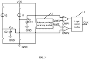
- the oscillator circuit includes: two charge and discharge circuits, a reference voltage switching module 2, two comparators and a logic control module 4.
- the two charge and discharge circuits are respectively a first charge and discharge circuit 11 and a second charge and discharge circuit 12, and the two comparators are respectively a first comparator CMP1 and a second comparator CMP2.
- the first charge and discharge circuit 11, the second charge and discharge circuit 12, and the reference voltage switching module 2 are respectively connected to a voltage source VDD.
- the first charge and discharge circuit 11 is connected to a first input terminal of the first comparator CMP1, that is, to a negative input terminal of the first comparator CMP1.
- the second charge and discharge circuit 12 is connected to a first input terminal of the second comparator CMP2, that is, to a negative input terminal of the second comparator CMP2.
- the reference voltage switching module 2 is connected to a second input terminal of each of the two comparators respectively, that is, to a positive input terminal of the first comparator CMP1 and a positive input terminal of the second comparator CMP2.
- the output terminals of the first comparator CMP1 and the second comparator CMP2 are respectively connected to the logic control module 4.
- the logic control module 4 is further connected to the two charge and discharge circuits and the reference voltage switching module 2 (not shown in the figure).
- the reference voltage switching module 2 is configured to output a reference voltage Vrefl to the first comparator CMP1 and a reference voltage Vref2 to the second comparator CMP2, that is, the reference voltage switching module 2 may control the reference voltages of both the first comparator CMP1 and the second comparator CMP2.
- the logic control module 4 is configured to control one charge and discharge circuit connected to each of the comparators to start discharging when the output of each of the comparators whose reference voltage is a first voltage transitions, control the other charge and discharge circuit to start charging, and control the reference voltage switching module 2 to switch the reference voltage of each of the comparators to a second voltage.
- the logic control module 4 is further configured to control one charge and discharge circuit to start charging when the output of each of the comparators transitions again.
- the logic control module 4 is further configured to control the reference voltage switching module to switch the reference voltage of each of the comparators to the first voltage when the output of each of the comparators transitions again, and control one charge and discharge circuit to stop charging.
- the first charge and discharge circuit 11 has the same structure as the second charge and discharge circuit 12.
- Each of the two charge and discharge circuits includes: a current control module and a charging capacitor.
- a first terminal of the current control module is configured to connect to a voltage source, a second terminal of the current control module is connected to a first terminal of the charging capacitor, and a second terminal of the charging capacitor is grounded.
- a connection between the current control module and the charging capacitor in the first charge and discharge circuit 11 is connected to the first input terminal of the first comparator CMP1.
- a connection between the current control module and the charging capacitor in the second charge and discharge circuit 12 is connected to the first input terminal of the second comparator CMP2.
- the first charge and discharge circuit 11 includes a resistor R1 and a capacitor C1
- the second charge and discharge circuit 12 includes a resistor R2 and a capacitor C2. It should be noted that in this embodiment, resistance values of the resistor R1 and the resistor R2 are generally set to be equal, and capacitance values of the capacitor C1 and the capacitor C2 are generally set to be equal.
- a first terminal of the resistor R1 and a first terminal of the resistor R2 are respectively connected to the voltage source VDD.
- a second terminal of the resistor R1 is connected to a first terminal of the capacitor C1, and a second terminal of the capacitor C1 is grounded to GND.
- a connection between the resistor R1 and the capacitor C1 is connected to a positive input terminal of the first comparator CMP1.
- a second terminal of the resistor R2 is connected to a first terminal of the capacitor C2, and a second terminal of the capacitor C2 is grounded to GND.
- a connection between the resistor R2 and the capacitor C2 is connected to a positive input terminal of the second comparator CMP2.
- the reference voltages of both the first comparator CMP1 and the second comparator CMP2 are a first voltage V h , and an initial state is that the capacitor C1 is charged to the first voltage V h and the capacitor C2 is charged to a second voltage V l , which are taken as an example to be specificly described below:
- a first cycle of the oscillator circuit is taken as an example.
- the logic control module 4 controls the first charge and discharge circuit 11 and the second charge and discharge circuit 12 to start charging respectively, that is, controls the voltage source VDD to start charging the capacitor C1 and the capacitor C2 respectively, and controls the second charge and discharge circuit to stop charging when a voltage across both terminals of the capacitor C2 reaches the second voltage V l , that is, to stop charging the capacitor C2 when the voltage across both terminals of the capacitor C2 reaches the second voltage V l .
- the voltage V C2 across both terminals of the capacitor C2 is actually V l +V d .
- the oscillator circuit reaches the initial state and enters a first half cycle of the first cycle.
- the logic control module 4 controls the capacitor C1 in the first charge and discharge circuit 11 connected to the first comparator CMP1 to start discharging, and controls the capacitor C2 in the second charge and discharge circuit 12 to start charging, while controlling the reference voltage switching module 2 to switch the reference voltage of the first comparator CMP1 to the second voltage V l .
- the capacitor C1 starts discharging from V h +V d .
- the logic control module 4 controls the reference voltage switching module 2 to switch the reference voltage of the first comparator CMP1 to the first voltage Vh, and controls the voltage source VDD to stop charging the capacitor C1, and the voltage across both terminals of the capacitor C1 is V l +V d .
- the capacitor C2 In the first half cycle, the capacitor C2 is always in a charging state. Since the reference voltage of the second comparator CMP2 is the first voltage V h , the output of the second comparator CMP2 is always at a low level.
- the logic control module 4 controls the capacitor C2 in the second charge and discharge circuit 12 connected to the second comparator CMP2 to start discharging, and controls the capacitor C1 in the first charge and discharge circuit 11 to start charging, while controlling the reference voltage switching module 2 to switch the reference voltage of the second comparator CMP2 to the second voltage V l .
- the capacitor C2 starts discharging from V h +V d .
- the output of the second comparator CMP2 transitions from a high level to a low level. Due to the existence of the delay time V d , the voltage V C2 across both terminals of the capacitor C2 is actually V l -V d ' (where Vd' represents the discharging voltage difference caused by T d ), and the voltage source VDD is controlled to charge the capacitor C2. When the capacitor C2 is charged to the second voltage V l , the output of the second comparator CMP2 transitions from a low level to a high level again.
- the logic control module 4 controls the reference voltage switching module 2 to switch the reference voltage of the second comparator CMP2 to the first voltage V h , and controls the voltage source VDD to stop charging the capacitor C2.
- the voltage V C2 across both terminals of the capacitor C2 is V l +V d .
- the capacitor C1 is always in the charging state. Since the reference voltage of the first comparator CMP1 is the first voltage V h , the output of the first comparator CMP1 is always at the low level.
- Vrefl represents the reference voltage of the first comparator CMP1
- Vref2 represents the reference voltage of the second comparator CMP2.
- each of the first charge and discharge circuit and the second charge discharge circuit further includes a first switch module S1 and a second switch module S2.
- the first terminal of the current control module is connected to the voltage source VDD through the first switch module S1.
- the connection between the current control module and the charging capacitor in each of the first charge and discharge circuit and the second charge discharge circuit is grounded through the second switch module S2.
- the logic control module 4 is further connected to a control terminal of the first switch module S1 and a control terminal of the second switch module S2 respectively.
- the logic control module 4 is configured to control the charge and discharge circuit to start charging by controlling the first switch module S1 to be turned on and the second switch module S2 to be turned off in the charge and discharge circuit. Taking the first charge and discharge circuit 11 as an example, the logic control module 4 controls the first charge and discharge circuit 11 to start charging by controlling the first switching module S1 to be turned on and the second switching module S2 to be turned off in the first charge and discharge circuit 11.
- the logic control module 4 is configured to control the charge and discharge circuit to start discharging by controlling the first switch module S1 to be turned off and the second switch module S2 to be turned on in the charge and discharge circuit. Taking the first charge and discharge circuit 11 as an example, the logic control module 4 controls the first charge and discharge circuit 11 to start discharging by controlling the first switching module S1 to be turned off and the second switching module S2 to be turned on in the first charge and discharge circuit 11.
- the logic control module 4 controls the voltage source VDD to charge the capacitor C1 by controlling the first switch module S1 to be turned on and the second switch module S2 to be turned off in the first charge and discharge circuit 11.
- the logic control module 4 controls the capacitor C1 to discharge by controlling the first switch module S1 to be turn off and the second switch module S2 to be turned on in the first charge and discharge circuit 11.
- the way in which the logic control module 4 controls the charging and discharging of the capacitor C2 is similar to the above, and will not be repeated here.
- T Vh is a time in which the capacitor is charged from 0 to the first voltage V h
- T Vl is a time in which the capacitor is charged from 0 to the second voltage V l
- R represents a resistance value of the resistor in the charge and discharge circuit
- C represents a capacitance value of the capacitor C1 or C2.
- T half the cycle length of the oscillator circuit in this embodiment has nothing to do with the delay time T d between the comparator and the logic control module 4, that is, an error source (i.e., the delay time T d ) that limits the accuracy of the oscillator circuit is eliminated, so that compared with the double capacitor oscillator circuit in FIG. 1 , a higher accuracy may be achieved under the same current.
- an error source i.e., the delay time T d
- the logic control module may control the first charge and discharge circuit connected to the first comparator to start discharging when the output of the first comparator whose reference voltage is the first voltage transitions, control the second charge and discharge circuit to start charging, and control the reference voltage switching module to switch the reference voltage of the first comparator to the second voltage according to the embodiment.
- the first charge and discharge circuit connected to the first comparator is controlled to charge.
- the reference voltage switching module is controlled to switch the reference voltage of the first comparator to the first voltage, and the first charge and discharge circuit is controlled to stop charging.
- the similar operation is repeated.
- the reference voltage of the comparator is switched and controlled, and the delay time that affects the accuracy in the oscillator circuit is eliminated by subtracting delay times of the comparator at different reference voltages from each other, thus improving the accuracy of the oscillator circuit.
- a second embodiment of the present disclosure relates to an oscillator circuit. Compared with the first embodiment, a main difference of this embodiment is that a current control module in a charge and discharge circuit is a current source.
- a first charge and discharge circuit 11 includes a current source I1 and a capacitor C1
- a second charge and discharge circuit 12 includes a current source 12 and a capacitor C2. It should be noted that in this embodiment, currents of the current source I1 and the current source 12 are generally set to be equal, and capacitance values of the capacitor C1 and the capacitor C2 are generally set to be equal.
- a first terminal of the current source I1 and a first terminal of the current source 12 are respectively connected to a voltage source VDD.
- a second terminal of the current source I1 is connected to a first terminal of the capacitor C1, a second terminal of the capacitor C1 is grounded, and a connection between the current source I1 and the capacitor C1 is connected to a positive input terminal of a first comparator CMP1.
- a second terminal of the current source 12 is connected to a first terminal of the capacitor C2, a second terminal of the capacitor C2 is grounded, and a connection between the current source 12 and the capacitor C2 is connected to a positive input terminal of a second comparator CMP2.
- each of the two charge and discharge circuits further including a first switch module S1 and a second switch module S2 is taken as an example for description.
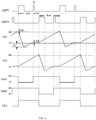
- a working mode of the oscillator circuit in FIG. 5 in one cycle is similar to that in FIG. 3 , and will not be repeated here.
- Vrefl represents a reference voltage of the first comparator CMP1
- Vref2 represents a reference voltage of the second comparator CMP2.
- T Vh is a time in which the capacitor is charged from 0 to a first voltage V h
- T Vl is a time in which the capacitor is charged from 0 to a second voltage V l
- I represents a discharge current of the current source in the charge and discharge circuit
- C represents a capacitance value of the capacitor C1 or C2.
- T half the cycle time of the oscillator circuit in this embodiment has nothing to do with the delay time T d between the comparator and the logic control module 4, that is, an error source (i.e., the delay time T d ) that limits the accuracy of the oscillator circuit is eliminated, so that compared with the double capacitor oscillator circuit in FIG. 1 , ahigher accuracy may be achieved under the same current.
- an error source i.e., the delay time T d
- this embodiment provides the oscillator circuit in which the current control module in the charge and discharge circuit is a current source.
- a third embodiment of the present disclosure relates to an oscillator circuit.
- a reference voltage switching module 2 includes a reference voltage generating circuit 21 and a reference voltage control circuit 22.
- Two output terminals of the reference voltage generating circuit 21 are respectively connected to two input terminals of the reference voltage control circuit 22.
- An input terminal of the reference voltage generating circuit 21 is connected to a voltage source VDD, and the reference voltage generating circuit 21 is also grounded to GND
- Two output terminals of the reference voltage control circuit 22 are respectively connected to the second input terminals of two comparators, that is, the two output terminals of the reference voltage control circuit 22 are respectively connected to a positive input terminal of a first comparator CMP1 and a positive input terminal of a second comparator CMP2.
- the reference voltage generating circuit 21 is configured to generate a first voltage V h and a second voltage V l , and output the first voltage V h and the second voltage V l to the reference voltage control circuit 22.
- a logic control module 4 is configured to control the reference voltage control circuit 22 to switch a reference voltage of each of the comparators.
- the reference voltage generating circuit 21 includes a current control module 211, a first resistor R3 and a second resistor R4 connected in sequence.
- a first terminal of the current control module 211 is configured to connect to the voltage source VDD, and a second terminal of the current control module 211 is connected to a first terminal of the first resistor R3.
- a second terminal of the first resistor R3 is connected to a first terminal of the second resistor R4, and a second terminal of the second resistor R4 is grounded.
- the two terminals of the first resistor R3 form two output terminals of the reference voltage generating circuit 22, that is, the first terminal of the first resistor R3 outputs the first voltage V h to the reference voltage control circuit 22, and the second terminal of the first resistor R3 outputs the second voltage V l to the reference voltage control circuit 22.
- the current control module 211 may be a resistor or a current source.
- this embodiment provides a specific implementation of the reference voltage switching module. It should be noted that this embodiment may also be used as an improvement on the basis of the second embodiment to achieve the same technical effect.
- a fourth embodiment of the present disclosure relates to a chip, which includes the oscillator circuit.
- a fifth embodiment of the present disclosure relates to an electronic device, which includes the chip of the fourth embodiment.
Landscapes
- Physics & Mathematics (AREA)
- Nonlinear Science (AREA)
- Electronic Switches (AREA)
- Inductance-Capacitance Distribution Constants And Capacitance-Resistance Oscillators (AREA)
- Dc-Dc Converters (AREA)
Applications Claiming Priority (1)
| Application Number | Priority Date | Filing Date | Title |
|---|---|---|---|
| PCT/CN2019/119486 WO2021097673A1 (zh) | 2019-11-19 | 2019-11-19 | 振荡电路、芯片、电子设备 |
Publications (2)
| Publication Number | Publication Date |
|---|---|
| EP3852268A4 EP3852268A4 (de) | 2021-07-21 |
| EP3852268A1 true EP3852268A1 (de) | 2021-07-21 |
Family
ID=70427272
Family Applications (1)
| Application Number | Title | Priority Date | Filing Date |
|---|---|---|---|
| EP19929186.5A Withdrawn EP3852268A1 (de) | 2019-11-19 | 2019-11-19 | Oszillatorschaltung, chip und elektronische vorrichtung |
Country Status (4)
| Country | Link |
|---|---|
| US (1) | US11245360B2 (de) |
| EP (1) | EP3852268A1 (de) |
| CN (1) | CN111108684A (de) |
| WO (1) | WO2021097673A1 (de) |
Families Citing this family (9)
| Publication number | Priority date | Publication date | Assignee | Title |
|---|---|---|---|---|
| CN111108684A (zh) * | 2019-11-19 | 2020-05-05 | 深圳市汇顶科技股份有限公司 | 振荡电路、芯片、电子设备 |
| CN111953315B (zh) * | 2020-09-08 | 2024-02-20 | 深圳市汇顶科技股份有限公司 | 晶体振荡器、芯片和电子设备 |
| WO2022051913A1 (zh) * | 2020-09-08 | 2022-03-17 | 深圳市汇顶科技股份有限公司 | 晶体振荡器、芯片和电子设备 |
| CN115065340A (zh) * | 2022-07-14 | 2022-09-16 | 华大恒芯科技有限公司 | 一种振荡电路 |
| CN115333510A (zh) * | 2022-08-19 | 2022-11-11 | 苏州聚元微电子股份有限公司 | 一种共享比较器的张弛振荡器 |
| CN115940619B (zh) * | 2023-01-10 | 2023-07-04 | 深圳市思远半导体有限公司 | 芯片、直流-直流电路及其控制方法 |
| CN116318057A (zh) * | 2023-03-03 | 2023-06-23 | 中国电子科技集团公司第二十四研究所 | 一种具有精确高占空比输出的振荡器电路 |
| CN116169953A (zh) * | 2023-04-24 | 2023-05-26 | 苏州萨沙迈半导体有限公司 | 振荡器电路、芯片和电子设备 |
| CN120750328B (zh) * | 2025-08-26 | 2025-11-21 | 无锡市晶源微电子股份有限公司 | 压控振荡电路及开关电源 |
Family Cites Families (11)
| Publication number | Priority date | Publication date | Assignee | Title |
|---|---|---|---|---|
| JP2002140131A (ja) * | 2000-11-01 | 2002-05-17 | Sony Corp | クロック生成回路及びそれを用いた昇圧回路 |
| US7746130B2 (en) * | 2008-07-14 | 2010-06-29 | Elite Semiconductor Memory Technology, Inc. | Triangular wave generating circuit having synchronization with external clock |
| CN102158203A (zh) * | 2011-04-26 | 2011-08-17 | 杭州芯赛微电子有限公司 | 一种高精度rc振荡器 |
| JP2013038744A (ja) * | 2011-08-11 | 2013-02-21 | Renesas Electronics Corp | 発振回路及びそれを備えた半導体集積回路 |
| CN102324912A (zh) * | 2011-08-13 | 2012-01-18 | 中科芯集成电路股份有限公司 | 电流控制振荡器 |
| US9099994B2 (en) * | 2012-12-20 | 2015-08-04 | Silicon Laboratories Inc. | Relaxation oscillator |
| CN103546123B (zh) * | 2013-11-01 | 2015-12-02 | 东南大学 | 一种高线性度的张弛振荡器 |
| CN105071786B (zh) * | 2015-07-30 | 2018-01-09 | 北京大学 | 一种采用半周期预充电补偿技术的电阻电容型弛豫振荡器 |
| US10135428B2 (en) * | 2016-08-31 | 2018-11-20 | Texas Instruments Incorporated | Methods and apparatus for a low power relaxation oscillator |
| CN108964610B (zh) * | 2018-06-29 | 2021-11-26 | 南京中感微电子有限公司 | 振荡电路 |
| CN111108684A (zh) * | 2019-11-19 | 2020-05-05 | 深圳市汇顶科技股份有限公司 | 振荡电路、芯片、电子设备 |
-
2019
- 2019-11-19 CN CN201980004378.XA patent/CN111108684A/zh active Pending
- 2019-11-19 WO PCT/CN2019/119486 patent/WO2021097673A1/zh not_active Ceased
- 2019-11-19 EP EP19929186.5A patent/EP3852268A1/de not_active Withdrawn
-
2020
- 2020-11-30 US US17/107,840 patent/US11245360B2/en not_active Expired - Fee Related
Also Published As
| Publication number | Publication date |
|---|---|
| WO2021097673A1 (zh) | 2021-05-27 |
| US20210152124A1 (en) | 2021-05-20 |
| EP3852268A4 (de) | 2021-07-21 |
| US11245360B2 (en) | 2022-02-08 |
| CN111108684A (zh) | 2020-05-05 |
Similar Documents
| Publication | Publication Date | Title |
|---|---|---|
| US11245360B2 (en) | Oscillator circuit, chip and electronic device | |
| CN107204755B (zh) | 一种高精度自适应的张弛振荡器 | |
| US7733191B2 (en) | Oscillator devices and methods thereof | |
| CN105071786B (zh) | 一种采用半周期预充电补偿技术的电阻电容型弛豫振荡器 | |
| US7486151B2 (en) | Semiconductor circuit for use in timer circuit or oscillator circuit | |
| US4428040A (en) | Low power consumption electronic circuit | |
| US9461632B2 (en) | Oscillator circuit | |
| CN113346878A (zh) | 时钟电路及电子设备 | |
| US9306493B2 (en) | Oscillator circuit | |
| US7474162B2 (en) | RC-oscillator circuit | |
| JP3963421B2 (ja) | 制御発振システムとその方法 | |
| US10879858B2 (en) | Oscillator circuit using comparator | |
| CN211791469U (zh) | 振荡器电路及开关霍尔传感器 | |
| CN108649900B (zh) | 一种振荡器链路延时校正电路 | |
| KR20030072527A (ko) | 직류-직류 컨버터의 발진기 | |
| CN113691220B (zh) | 片上低频振荡器 | |
| US10771046B2 (en) | Comparator and oscillator circuit using said comparator | |
| CN115296617A (zh) | 振荡电路及其控制方法 | |
| CN101018048A (zh) | 振荡电路 | |
| CN120049836B (zh) | 弛豫振荡器、芯片和电子设备 | |
| CN114244277A (zh) | 一种精确控制占空比的集成振荡器 | |
| JPH06224705A (ja) | 発振回路 | |
| JPH09121142A (ja) | 発振回路 | |
| JPH09212247A (ja) | 基準電圧発生回路 | |
| CN116317951B (zh) | Rc张弛振荡器电路 |
Legal Events
| Date | Code | Title | Description |
|---|---|---|---|
| STAA | Information on the status of an ep patent application or granted ep patent |
Free format text: STATUS: UNKNOWN |
|
| STAA | Information on the status of an ep patent application or granted ep patent |
Free format text: STATUS: THE INTERNATIONAL PUBLICATION HAS BEEN MADE |
|
| PUAI | Public reference made under article 153(3) epc to a published international application that has entered the european phase |
Free format text: ORIGINAL CODE: 0009012 |
|
| STAA | Information on the status of an ep patent application or granted ep patent |
Free format text: STATUS: REQUEST FOR EXAMINATION WAS MADE |
|
| 17P | Request for examination filed |
Effective date: 20201125 |
|
| A4 | Supplementary search report drawn up and despatched |
Effective date: 20210601 |
|
| AK | Designated contracting states |
Kind code of ref document: A1 Designated state(s): AL AT BE BG CH CY CZ DE DK EE ES FI FR GB GR HR HU IE IS IT LI LT LU LV MC MK MT NL NO PL PT RO RS SE SI SK SM TR |
|
| STAA | Information on the status of an ep patent application or granted ep patent |
Free format text: STATUS: THE APPLICATION HAS BEEN WITHDRAWN |
|
| 18W | Application withdrawn |
Effective date: 20211201 |