EP3862360A1 - Organometallische verbindung, organische lichtemittierende vorrichtung damit und elektronische einrichtung mit der organischen lichtemittierenden vorrichtung - Google Patents
Organometallische verbindung, organische lichtemittierende vorrichtung damit und elektronische einrichtung mit der organischen lichtemittierenden vorrichtung Download PDFInfo
- Publication number
- EP3862360A1 EP3862360A1 EP21155700.4A EP21155700A EP3862360A1 EP 3862360 A1 EP3862360 A1 EP 3862360A1 EP 21155700 A EP21155700 A EP 21155700A EP 3862360 A1 EP3862360 A1 EP 3862360A1
- Authority
- EP
- European Patent Office
- Prior art keywords
- group
- substituted
- formula
- alkyl
- unsubstituted
- Prior art date
- Legal status (The legal status is an assumption and is not a legal conclusion. Google has not performed a legal analysis and makes no representation as to the accuracy of the status listed.)
- Granted
Links
- 0 CC(C)c1c(*)cccc1 Chemical compound CC(C)c1c(*)cccc1 0.000 description 22
- KMTBIOPNNMUVFI-UHFFFAOYSA-N CC(C1)C=Cc2c1c(cc(cc1)N(c3ccc(C)cc3)c(cc3)ccc3-c(cc3)ccc3N(c3ccc(C)cc3)c(cc3)cc(c4c5cccc4)c3[n]5-c3ccccc3)c1[n]2-c1ccccc1 Chemical compound CC(C1)C=Cc2c1c(cc(cc1)N(c3ccc(C)cc3)c(cc3)ccc3-c(cc3)ccc3N(c3ccc(C)cc3)c(cc3)cc(c4c5cccc4)c3[n]5-c3ccccc3)c1[n]2-c1ccccc1 KMTBIOPNNMUVFI-UHFFFAOYSA-N 0.000 description 1
- ICSNLGPSRYBMBD-UHFFFAOYSA-N Nc1ccccn1 Chemical compound Nc1ccccn1 ICSNLGPSRYBMBD-UHFFFAOYSA-N 0.000 description 1
- CUYKNJBYIJFRCU-UHFFFAOYSA-N Nc1cccnc1 Chemical compound Nc1cccnc1 CUYKNJBYIJFRCU-UHFFFAOYSA-N 0.000 description 1
- NUKYPUAOHBNCPY-UHFFFAOYSA-N Nc1ccncc1 Chemical compound Nc1ccncc1 NUKYPUAOHBNCPY-UHFFFAOYSA-N 0.000 description 1
- FVLAYJRLBLHIPV-UHFFFAOYSA-N Nc1cncnc1 Chemical compound Nc1cncnc1 FVLAYJRLBLHIPV-UHFFFAOYSA-N 0.000 description 1
- HXPARCXOHJXWFN-UHFFFAOYSA-N c(cc1)ccc1-[n]1c(ccc(N(c(cc2)ccc2-c(cc2)ccc2N(c(cc2c3c4cccc3)ccc2[n]4-c2ccccc2)c2cccc3c2cccc3)c2cccc3c2cccc3)c2)c2c2ccccc12 Chemical compound c(cc1)ccc1-[n]1c(ccc(N(c(cc2)ccc2-c(cc2)ccc2N(c(cc2c3c4cccc3)ccc2[n]4-c2ccccc2)c2cccc3c2cccc3)c2cccc3c2cccc3)c2)c2c2ccccc12 HXPARCXOHJXWFN-UHFFFAOYSA-N 0.000 description 1
- AEABXZMGEOGKKE-UHFFFAOYSA-N c(cc1)ccc1-c(cc1)ccc1N(c(cc1)ccc1-c(cc1)ccc1N(c(cc1)ccc1-c1ccccc1)c(cc1)cc(c2ccccc22)c1[n]2-c1ccccc1)c(cc1c2ccccc22)ccc1[n]2-c1ccccc1 Chemical compound c(cc1)ccc1-c(cc1)ccc1N(c(cc1)ccc1-c(cc1)ccc1N(c(cc1)ccc1-c1ccccc1)c(cc1)cc(c2ccccc22)c1[n]2-c1ccccc1)c(cc1c2ccccc22)ccc1[n]2-c1ccccc1 AEABXZMGEOGKKE-UHFFFAOYSA-N 0.000 description 1
- MESMXXUBQDBBSR-UHFFFAOYSA-N c(cc1)ccc1N(c(cc1)ccc1-c(cc1)ccc1N(c1ccccc1)c(cc1)cc(c2ccccc22)c1[n]2-c1ccccc1)c(cc1c2c3cccc2)ccc1[n]3-c1ccccc1 Chemical compound c(cc1)ccc1N(c(cc1)ccc1-c(cc1)ccc1N(c1ccccc1)c(cc1)cc(c2ccccc22)c1[n]2-c1ccccc1)c(cc1c2c3cccc2)ccc1[n]3-c1ccccc1 MESMXXUBQDBBSR-UHFFFAOYSA-N 0.000 description 1
Images
Classifications
-
- C—CHEMISTRY; METALLURGY
- C07—ORGANIC CHEMISTRY
- C07F—ACYCLIC, CARBOCYCLIC OR HETEROCYCLIC COMPOUNDS CONTAINING ELEMENTS OTHER THAN CARBON, HYDROGEN, HALOGEN, OXYGEN, NITROGEN, SULFUR, SELENIUM OR TELLURIUM
- C07F15/00—Compounds containing elements of Groups 8, 9, 10 or 18 of the Periodic Table
- C07F15/0006—Compounds containing elements of Groups 8, 9, 10 or 18 of the Periodic Table compounds of the platinum group
- C07F15/0033—Iridium compounds
-
- C—CHEMISTRY; METALLURGY
- C09—DYES; PAINTS; POLISHES; NATURAL RESINS; ADHESIVES; COMPOSITIONS NOT OTHERWISE PROVIDED FOR; APPLICATIONS OF MATERIALS NOT OTHERWISE PROVIDED FOR
- C09K—MATERIALS FOR MISCELLANEOUS APPLICATIONS, NOT PROVIDED FOR ELSEWHERE
- C09K11/00—Luminescent materials, e.g. electroluminescent or chemiluminescent
- C09K11/06—Luminescent materials, e.g. electroluminescent or chemiluminescent containing organic luminescent materials
-
- H—ELECTRICITY
- H10—SEMICONDUCTOR DEVICES; ELECTRIC SOLID-STATE DEVICES NOT OTHERWISE PROVIDED FOR
- H10K—ORGANIC ELECTRIC SOLID-STATE DEVICES
- H10K50/00—Organic light-emitting devices
- H10K50/10—OLEDs or polymer light-emitting diodes [PLED]
- H10K50/11—OLEDs or polymer light-emitting diodes [PLED] characterised by the electroluminescent [EL] layers
-
- H—ELECTRICITY
- H10—SEMICONDUCTOR DEVICES; ELECTRIC SOLID-STATE DEVICES NOT OTHERWISE PROVIDED FOR
- H10K—ORGANIC ELECTRIC SOLID-STATE DEVICES
- H10K50/00—Organic light-emitting devices
- H10K50/10—OLEDs or polymer light-emitting diodes [PLED]
- H10K50/11—OLEDs or polymer light-emitting diodes [PLED] characterised by the electroluminescent [EL] layers
- H10K50/12—OLEDs or polymer light-emitting diodes [PLED] characterised by the electroluminescent [EL] layers comprising dopants
-
- H—ELECTRICITY
- H10—SEMICONDUCTOR DEVICES; ELECTRIC SOLID-STATE DEVICES NOT OTHERWISE PROVIDED FOR
- H10K—ORGANIC ELECTRIC SOLID-STATE DEVICES
- H10K50/00—Organic light-emitting devices
- H10K50/10—OLEDs or polymer light-emitting diodes [PLED]
- H10K50/14—Carrier transporting layers
-
- H—ELECTRICITY
- H10—SEMICONDUCTOR DEVICES; ELECTRIC SOLID-STATE DEVICES NOT OTHERWISE PROVIDED FOR
- H10K—ORGANIC ELECTRIC SOLID-STATE DEVICES
- H10K50/00—Organic light-emitting devices
- H10K50/10—OLEDs or polymer light-emitting diodes [PLED]
- H10K50/14—Carrier transporting layers
- H10K50/16—Electron transporting layers
-
- H—ELECTRICITY
- H10—SEMICONDUCTOR DEVICES; ELECTRIC SOLID-STATE DEVICES NOT OTHERWISE PROVIDED FOR
- H10K—ORGANIC ELECTRIC SOLID-STATE DEVICES
- H10K85/00—Organic materials used in the body or electrodes of devices covered by this subclass
- H10K85/30—Coordination compounds
- H10K85/341—Transition metal complexes, e.g. Ru(II)polypyridine complexes
- H10K85/342—Transition metal complexes, e.g. Ru(II)polypyridine complexes comprising iridium
-
- H—ELECTRICITY
- H10—SEMICONDUCTOR DEVICES; ELECTRIC SOLID-STATE DEVICES NOT OTHERWISE PROVIDED FOR
- H10K—ORGANIC ELECTRIC SOLID-STATE DEVICES
- H10K85/00—Organic materials used in the body or electrodes of devices covered by this subclass
- H10K85/40—Organosilicon compounds, e.g. TIPS pentacene
-
- C—CHEMISTRY; METALLURGY
- C09—DYES; PAINTS; POLISHES; NATURAL RESINS; ADHESIVES; COMPOSITIONS NOT OTHERWISE PROVIDED FOR; APPLICATIONS OF MATERIALS NOT OTHERWISE PROVIDED FOR
- C09K—MATERIALS FOR MISCELLANEOUS APPLICATIONS, NOT PROVIDED FOR ELSEWHERE
- C09K2211/00—Chemical nature of organic luminescent or tenebrescent compounds
- C09K2211/18—Metal complexes
- C09K2211/185—Metal complexes of the platinum group, i.e. Os, Ir, Pt, Ru, Rh or Pd
-
- H—ELECTRICITY
- H10—SEMICONDUCTOR DEVICES; ELECTRIC SOLID-STATE DEVICES NOT OTHERWISE PROVIDED FOR
- H10K—ORGANIC ELECTRIC SOLID-STATE DEVICES
- H10K2101/00—Properties of the organic materials covered by group H10K85/00
- H10K2101/10—Triplet emission
-
- H—ELECTRICITY
- H10—SEMICONDUCTOR DEVICES; ELECTRIC SOLID-STATE DEVICES NOT OTHERWISE PROVIDED FOR
- H10K—ORGANIC ELECTRIC SOLID-STATE DEVICES
- H10K30/00—Organic devices sensitive to infrared radiation, light, electromagnetic radiation of shorter wavelength or corpuscular radiation
- H10K30/30—Organic devices sensitive to infrared radiation, light, electromagnetic radiation of shorter wavelength or corpuscular radiation comprising bulk heterojunctions, e.g. interpenetrating networks of donor and acceptor material domains
- H10K30/353—Organic devices sensitive to infrared radiation, light, electromagnetic radiation of shorter wavelength or corpuscular radiation comprising bulk heterojunctions, e.g. interpenetrating networks of donor and acceptor material domains comprising blocking layers, e.g. exciton blocking layers
-
- H—ELECTRICITY
- H10—SEMICONDUCTOR DEVICES; ELECTRIC SOLID-STATE DEVICES NOT OTHERWISE PROVIDED FOR
- H10K—ORGANIC ELECTRIC SOLID-STATE DEVICES
- H10K50/00—Organic light-emitting devices
- H10K50/10—OLEDs or polymer light-emitting diodes [PLED]
- H10K50/14—Carrier transporting layers
- H10K50/15—Hole transporting layers
-
- H—ELECTRICITY
- H10—SEMICONDUCTOR DEVICES; ELECTRIC SOLID-STATE DEVICES NOT OTHERWISE PROVIDED FOR
- H10K—ORGANIC ELECTRIC SOLID-STATE DEVICES
- H10K50/00—Organic light-emitting devices
- H10K50/10—OLEDs or polymer light-emitting diodes [PLED]
- H10K50/17—Carrier injection layers
- H10K50/171—Electron injection layers
Definitions
- One or more embodiments relate to an organometallic compound, an organic light-emitting device including the same, and an electronic apparatus including the organic light-emitting device.
- OLEDs Organic light-emitting devices
- OLEDs are self-emission devices, which have improved characteristics in terms of viewing angles, response times, brightness, driving voltage, and response speeds, and produce full-color images.
- an organic light-emitting device includes an anode, a cathode, and an organic layer disposed between the anode and the cathode, wherein the organic layer includes an emission layer.
- a hole transport region may be disposed between the anode and the emission layer, and an electron transport region may be disposed between the emission layer and the cathode.
- Holes provided from the anode may move toward the emission layer through the hole transport region, and electrons provided from the cathode may move toward the emission layer through the electron transport region.
- the holes and the electrons recombine in the emission layer to produce excitons. These excitons transit from an excited state to a ground state, thereby generating light.
- One or more embodiments relate to an organometallic compound, an organic light-emitting device including the same, and an electronic apparatus including the organic light-emitting device.
- an organometallic compound represented by Formula 1 is provided.
- M is a transition metal
- L 1 is a ligand represented by Formula 2
- n1 is 1, 2, or 3, wherein, when n1 is 2 or greater, two or more of ligands L 1 may be identical to or different from each other
- L 2 is a monodentate ligand, a bidentate ligand, a tridentate ligand, or a tetradentate ligand
- n2 is 0, 1, 2, 3, or 4, wherein, when n2 is 2 or greater, two or more of ligands L 2 are identical to or different from each other, and L 1 and L 2 are different from each other, wherein, in Formula 2,
- an organic light-emitting device including a first electrode, a second electrode, and an organic layer disposed between the first electrode and the second electrode and including an emission layer, wherein the organic layer includes at least one organometallic compound represented by Formula 1.
- the organometallic compound may be included in the emission layer, and the organometallic compound included in the emission layer may act as a dopant.
- an electronic apparatus including the organic light-emitting device.
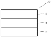
- FIGURE shows a schematic cross-sectional view of an organic light-emitting device according to one or more embodiments.
- first, second, third etc. may be used herein to describe various elements, components, regions, layers, and/or sections, these elements, components, regions, layers, and/or sections should not be limited by these terms. These terms are only used to distinguish one element, component, region, layer, or section from another element, component, region, layer, or section. Thus, a first element, component, region, layer, or section discussed below could be termed a second element, component, region, layer, or section without departing from the teachings of the present embodiments.
- An aspect of the present disclosure provides an organometallic compound represented by Formula 1: Formula 1 M(L 1 ) n1 (L 2 )n 2 M in Formula 1 is a transition metal.
- M may be a first-row transition metal of the Periodic Table of Elements, a second-row transition metal of the Periodic Table of Elements, or a third-row transition metal of the Periodic Table of Elements.
- M may be iridium (Ir), platinum (Pt), osmium (Os), titanium (Ti), zirconium (Zr), hafnium (Hf), europium (Eu), terbium (Tb), thulium (Tm), or rhodium (Rh).
- M may be Ir, Pt, Os, or Rh.
- L 1 in Formula 1 is a ligand represented by Formula 2.
- n1 in Formula 1 indicates the number of ligands L 1 and may be 1, 2, or 3. When n1 is 2 or greater, two or more ligands L 1 may be identical to or different from each other. For example, n1 may be 1 or 2.
- L 2 in Formula 1 may be a monodentate ligand, a bidentate ligand, a tridentate ligand, or a tetradentate ligand. L 2 is further described in the present specification below.
- n2 in Formula 1 indicates the number of ligands L 2 and may be 0,1, 2, 3, or 4. When n2 is 2 or greater, two or more ligands L 2 may be identical to or different from each other. For example, n2 may be 1 or 2.
- L 1 and L 2 in Formula 1 may be different from each other.
- M may be Ir or Os, and the sum of n1 and n2 may be 3 or 4; or M may be Pt, and the sum of n1 and n2 may be 2.
- M may be Ir, n1 and n2 may each independently be 1 or 2, and the sum of n1 and n2 may be 3.
- X 11 may be C bonded with X 1 in Formula 3 (via a single bond), N, or C(R 11 ),
- X 12 may be C bonded with X 1 or X 2 in Formula 3 (via a single bond), N, or C(R 12 )
- X 13 may be C bonded with X 1 or X 2 in Formula 3 (via a single bond), N, or C(R 13 )
- X 14 may be C bonded with X 2 in Formula 3 (via a single bond), N, or C(R 14 ).
- X 11 may be C bonded with X 1 in Formula 3 (via a single bond)
- X 12 may be C bonded with X 2 in Formula 3 (via a single bond)
- X 12 may be C bonded with X 1 in Formula 3 (via a single bond)
- X 13 may be C bonded with X 2 in Formula 3 (via a single bond)
- X 14 may be C bonded with X 2 in Formula 3 (via a single bond).
- a group represented by Formula 3 is necessarily condensed to the group represented by Formula 2.
- L 1 is actually a ligand obtained by condensing the group represented by Formula 3 to the group represented by Formula 2.
- X 1 may be O, S, Se, B(R 31 ), N(R 31 ), C(R 31 )(R 32 ), or Si(R 31 )(R 32 )
- X 2 may be O, S, Se, B(R 33 ), N(R 33 ), C(R 33 )(R 34 ), or Si(R 33 )(R 34 ).
- At least one of X 1 and X 2 in Formula 3 may be O, S, or Se.
- X 1 and X 2 in Formula 3 may be identical to each other.
- X 1 and X 2 in Formula 3 may be different from each other.
- X 1 may be C(R 31 )(R 32 ), and X 2 may be O, S, Se, B(R 33 ), N(R 33 ), or Si(R 33 )(R 34 ); or X 1 may be O, S, Se, B(R 31 ), N(R 31 ), or Si(R 31 )(R 32 ), and X 2 may be C(R 33 )(R 34 ).
- Y 1 may be N
- Y 2 may be C or N
- Y 2 in Formula 2 may be C.
- Ring CY 1 and ring CY 2 in Formulae 2 and 3 may each independently be a C 5 -C 30 carbocyclic group or a C 1 -C 30 heterocyclic group.
- ring CY 1 and ring CY 2 in Formulae 2 and 3 may each independently be a first ring, a second ring, a condensed ring in which two or more first rings are condensed with each other, a condensed ring in which two or more second rings are condensed with each other, or a condensed ring in which one or more first rings and one or more second rings are condensed with each other,
- the first ring may be a cyclopentane group, a cyclopentadiene group, a furan group, a thiophene group, a pyrrole group, a silole group, an indene group, a benzofuran group, a benzothiophene group, an indole group, a benzosilole group, an oxazole group, an isoxazole group, an oxadiazole group, an isoxadiazole group, an oxatriazole group, an isoxatriazole group, a thiazole group, an isothiazole group, a thiadiazole group, an isothiadiazole group, a thiatriazole group, an isothiatriazole group, a pyrazole group, an imidazole group, a triazole group, a tetrazole group, an azasilole group, a diazasil
- the second ring may be an adamantane group, a norbornane group, a norbornene group, a bicyclo[1.1.1]pentane group, a bicyclo[2.1.1]hexane group, a bicyclo[2.2.2]octane group, a cyclohexane group, a cyclohexene group, a benzene group, a pyridine group, a pyrimidine group, a pyrazine group, a pyridazine group, or a triazine group.
- ring CY 1 and ring CY 2 may each independently be a cyclopentane group, a cyclohexane group, a cycloheptane group, a cyclopentene group, a cyclohexene group, a cycloheptene group, an adamantane group, a norbornane group, a norbornene group, a bicyclo[1.1.1]pentane group, a bicyclo[2.1.1]hexane group, a bicyclo[2.2.2]octane group, a benzene group, a naphthalene group, an anthracene group, a phenanthrene group, a triphenylene group, a pyrene group, a chrysene group, a 1,2,3,4-tetrahydronaphthalene group, a pyrrole group, a borole group, a cyclopentane group,
- ring CY 1 in Formula 3 may be a benzene group, a pyridine group, or a pyrimidine group.
- Y 2 in Formula 2 may be C, and ring CY 2 in Formula 2 may be a benzene group, a naphthalene group, a fluorene group, a dibenzofuran group, a dibenzothiophene group, a carbazole group, or a dibenzosilole group.
- R 1 , R 2 , R 11 to R 14 , and R 31 to R 34 may each independently be hydrogen, deuterium, -F, -Cl, -Br, -I, -SF 5 , a hydroxyl group, a cyano group, a nitro group, an amino group, an amidino group, a hydrazine group, a hydrazone group, a carboxylic acid group or a salt thereof, a sulfonic acid group or a salt thereof, a phosphoric acid group or a salt thereof, a substituted or unsubstituted C 1 -C 60 alkyl group, a substituted or unsubstituted C 2 -C 60 alkenyl group, a substituted or unsubstituted C 2 -C 60 alkynyl group, a substituted or unsubstituted C 1 -C 60 alkoxy group, a substituted or unsubstituted C 3 -
- R 1 , R 2 , R 11 to R 14 , and R 31 to R 34 may each independently be:
- R 1 , R 2 , R 11 to R 14 , and R 31 to R 34 may each independently be hydrogen, deuterium, -F, a cyano group, a nitro group, -SF 5 , -CH 3 , -CD 3 , -CD 2 H, -CDH 2 , - CF 3 , -CF 2 H, -CFH 2 , a group represented by one of Formulae 9-1 to 9-66, a group represented by one of Formulae 9-1 to 9-66 in which at least one hydrogen is substituted with deuterium, a group represented by one of Formulae 10-1 to 10-118, a group represented by one of Formulae 10-1 to 10-118 in which at least one hydrogen is substituted with deuterium, a group represented by one of Formulae 10-201 to 10-342, a group represented by one of Formulae 10-201 to 10-342 in which at least one hydrogen is substituted with deuterium, -Si(Q 3 )(Q 4 )(Q 5 ), or
- the "group represented by one of Formulae 9-1 to 9-66 in which at least one hydrogen is substituted with deuterium” may be, for example, a group represented by one of Formulae 9-501 to 9-514 and 9-601 to 9-638:
- the "group represented by one of Formulae 10-1 to 10-118 in which at least one hydrogen is substituted with deuterium” may be, for example, a group represented by one of Formulae 10-501 to 10-546.
- a1 in Formula 3 indicates the number of groups R 1 and may be an integer from 0 to 10. When a1 is 2 or greater, two or more groups R 1 may be identical to or different from each other. For example, a1 may be 0, 1, or 2.
- a2 in Formula 2 indicates the number of groups R 2 and may be an integer from 0 to 20. When a2 is 2 or greater, two or more groups R 2 may be identical to or different from each other. For example, a2 may be an integer from 0 to 10.
- L 1 in Formula 1 may be a ligand represented by Formula 2-1, 2-2, or 2-3.
- X 11 may be N or C(R 11 )
- X 12 may be N or C(R 12 )
- X 13 may be N or C(R 13 )
- X 14 may be N or C(R 14 )
- X 1 , X 2 , Y 1 , Y 2 , ring CY 1 , ring CY 2 , R 1 , R 2 , R 11 to R 14 , a1, a2, *, and *' are the same as described in the present specification.
- L 1 in Formula 1 may be the ligand represented by Formula 2-3
- X 12 in Formula 2-3 may be C(R 12 )
- R 12 may be -Si(Q 3 )(Q 4 )(Q5) or -Ge(Q 3 )(Q 4 )(Q 5 ), wherein Q 3 to Q 5 are as provided herein.
- L 1 in Formula 1 may be a ligand represented by Formula 2-1(1), 2-2(1), or 2-3(1):
- X 1 , X 2 , Y 1 , Y 2 , ring CY 2 , R 1 , R 2 , R 11 to R 14 , a1, a2, *, and *' are the same as described in the present specification.
- a group represented by in Formula 2 may be a group represented by one of Formulae CY2-1 to CY2-31:
- Y 2 and R 2 are each the same as described above, X 22 is C(R 22 )(R 23 ), N(R 22 ), O, S, or Si(R 22 )(R 23 ), R 22 to R 29 are the same as described in connection with R 2 , a26 is an integer from 0 to 6, a25 is an integer from 0 to 5, a24 is an integer from 0 to 4, a23 is an integer from 0 to 3, a22 is an integer from 0 to 2, *" indicates a binding site to a neighboring atom in Formula 2, and * indicates a binding site to M in Formula 1.
- L 2 in Formula 1 may be a bidentate ligand bonded to M in Formula 1 via two atoms selected from O, S, N, C, P, Si, and As included therein.
- the two atoms may the same or different.
- L 2 in Formula 1 may be a bidentate ligand bonded to M in Formula 1 via two atoms selected from N and C included therein.
- L 2 in Formula 1 may be a group represented by one of Formulae 3A to 3F: *-c ⁇ c-z 1 3E
- Y 13 is O, N, N(Z 1 ), P(Z 1 )(Z 2 ), or As(Z 1 )(Z 2 )
- Y 14 is O, N, N(Z 3 ), P(Z 3 )(Z 4 ), or As(Z 3 )(Z 4 )
- a group represented by in Formula 3D may be a group represented by one of Formulae CY11-1 to CY11-34, and (or) a group represented by in Formulae 3C and 3D may be a group represented by one of Formulae CY12-1 to CY12-34:
- X 31 is O, S, N(Z 11 ), C(Z 11 )(Z 12 ), or Si(Z 11 )(Z 12 )
- X 41 is O, S, N(Z 21 ), C(Z 21 )(Z 22 ), or Si(Z 21 )(Z 22 )
- Y 11 , Y 12 , Z 1 , and Z 2 are the same as described in the present specification
- Z 11 to Z 18 and Z 21 to Z 28 are the same as described in connection with R 1 , d12 and d22 are each independently an integer from 0 to 2
- d13 and d23 are each independently an integer from 0 to 3
- d14 and d24 are each independently an integer from 0 to 4
- d15 and d25 are each independently an integer from 0 to 5
- d16 and d26 are each independently an integer from 0 to 6, and in Formulae CY11-1 to CY11-34 and CY12-1 to
- L 2 in Formula 1 may be the ligand represented by Formula 3D, and at least one of Z 1 and Z 2 in Formula 3D may each independently be: deuterium; - Si(Q 3 )(Q 4 )(Q 5 ); -Ge(Q 3 )(Q 4 )(Q 5 ); or a C 1 -C 60 alkyl group substituted with at least one deuterium.
- L 2 may be a ligand represented by one of Formulae 3-1 and 3-101 to 3-112:
- Y 11 , Y 12 , ring CY 12 , Z 1 to Z 4 , Z 11 to Z 13 , and d2 are the same as described in the present specification
- Z 14 is the same as described in connection with Z 11
- e2 is an integer from 0 to 2
- e3 is an integer from 0 to 3
- e4 is an integer from 0 to 4
- * and *' each indicate a binding site to M in Formula 1.
- Z 12 in Formula 3-1 may be: -Si(Q 3 )(Q 4 )(Q 5 ); -Ge(Q 3 )(Q 4 )(Q 5 ); or a deuterated C 1 -C 60 alkyl group.
- Z 12 may be -Si(Q 3) (Q 4 )(Q 5 ) or -Ge(Q 3 )(Q 4 )(Q 5 ), and Z 13 may not be hydrogen and a methyl group.
- a group represented by in Formula 3-1 may be a group represented by one of Formulae 3-1-1 to 3-1-16, and (or) a group represented by in Formula 3-1 may be a group represented by one of Formulae 3-1(1) to 3-1(16):
- Z 11 to Z 14 are the same as described in the present specification
- Z 21 to Z 24 are the same as described in connection with Z 11 , wherein Z 11 to Z 14 and Z 21 to Z 24 are not hydrogen
- * and *' each indicate a binding site to M in Formula 1
- *" indicates a binding site to a neighboring atom.
- the organometallic compound of Formula 1 does not include (i.e., excludes) a compound in which n2 in Formula 1 is 0, X 1 in Formula 3 is C(R 31 )(R 32 ), and X 2 in Formula 3 is C(R 33 )(R 34 ).
- two or more of a plurality of groups R 1 may optionally be linked together to form a C 5 -C 30 carbocyclic group unsubstituted or substituted with at least one R 10a or a C 1 -C 30 heterocyclic group unsubstituted or substituted with at least one R 10a ; and two or more of a plurality of groups R 2 may optionally be linked together to form a C 5 -C 30 carbocyclic group unsubstituted or substituted with at least one R 10a or a C 1 -C 30 heterocyclic group unsubstituted or substituted with at least one R 10a .
- R 10a is the same as described in connection with R 2
- * and *' in Formula 2 each indicate a binding site to M in Formula 1.
- * and *' in Formula 3 each indicate a binding site to two of X 11 to X 14 in Formula 2.
- the organometallic compound represented by Formula 1 may be one of Compounds 1 to 289:
- Compounds 10 to 289 are represented by Formula 1, wherein M is Ir, L 2 is a phenyl-pyridine ligand, and each of L 1 , n1, and n2 are as defined in Tables 1 to 8 below.
- Ph is a phenyl group
- Me is a methyl group
- TMS is a tri(methyl)silyl group
- CY2-1(1) and CY2-1(2) have the following formulae:
- L 1 is the ligand represented by Formula 2
- n1 indicating the number of ligands L 1 is 1, 2, or 3. That is, the organometallic compound necessarily includes at least one ligand represented by Formula 2, as a ligand linked to metal M.
- An electronic device for example, an organic light-emitting device, including the organometallic compound represented by Formula 1, may have improved driving voltage and improved external quantum efficiency.
- organometallic compounds of organometallic compounds represented by Formula 1 highest occupied molecular orbital (HOMO) energy levels and lowest unoccupied molecular orbital (LUMO) energy levels, and T 1 energy levels were evaluated using a Gaussian 09 program with molecular structure optimization by density function theory (DFT) based on B3LYP, and results thereof are shown in Table 9.
- Table 9 Compound No.
- organometallic compounds represented by Formula 1 have electrical characteristics that are suitable for use as a material of an electronic device, for example, a dopant for an emission layer of an organic light-emitting device.
- Synthesis methods of the organometallic compound represented by Formula 1 may be understood by one of ordinary skill in the art by referring to Synthesis Examples provided below.
- the organometallic compound represented by Formula 1 is suitable for use as a material of an organic light-emitting device, for example, a dopant for an emission layer in an organic layer of an organic light-emitting device.
- an organic light-emitting device including: a first electrode; a second electrode; and an organic layer located between the first electrode and the second electrode and including an emission layer, and the organic layer includes at least one organometallic compound represented by Formula 1.
- the organic light-emitting device may have, due to the inclusion of an organic layer including the organometallic compound represented by Formula 1, a low driving voltage, high luminescence efficiency, high power efficiency, high external quantum efficiency, a long lifespan, a low roll-off ratio, and excellent color purity.
- the organometallic compound represented by Formula 1 may be disposed between a pair of electrodes of an organic light-emitting device.
- the organometallic compound represented by Formula 1 may be included in the emission layer.
- the organometallic compound may act as a dopant, and the emission layer may further include a host (that is, an amount of the organometallic compound represented by Formula 1 is smaller than an amount of the host).
- the emission layer may emit red light or green light.
- the organometallic compound represented by Formula 1 may emit green light having a maximum emission wavelength in a range of about 500 nanometers (nm) to about 550 nm, for example, about 500 nm to about 540 nm.
- (an organic layer) includes at least one organometallic compound” used herein may include a case in which "(an organic layer) includes identical organometallic compounds represented by Formula 1" and a case in which "(an organic layer) includes two or more different organometallic compounds represented by Formula 1".
- the organic layer may include, as the organometallic compound, only Compound 1.
- Compound 1 may exist only in the emission layer of the organic light-emitting device.
- the organic layer may include, as the organometallic compound, Compound 1 and Compound 2.
- Compound 1 and Compound 2 may exist in an identical layer (for example, Compound 1 and Compound 2 both may exist in an emission layer).
- the first electrode may be an anode, which is a hole injection electrode
- the second electrode may be a cathode, which is an electron injection electrode
- the first electrode may be a cathode, which is an electron injection electrode
- the second electrode may be an anode, which is a hole injection electrode.
- the first electrode is an anode
- the second electrode is a cathode
- the organic layer may further include a hole transport region disposed between the first electrode and the emission layer and an electron transport region disposed between the emission layer and the second electrode
- the hole transport region may include a hole injection layer, a hole transport layer, an electron blocking layer, a buffer layer, or a combination thereof
- the electron transport region may include a hole blocking layer, an electron transport layer, an electron injection layer, or a combination thereof.
- organic layer refers to a single layer and/or a plurality of layers between the first electrode and the second electrode of the organic light-emitting device.
- the “organic layer” may include, in addition to an organic compound, an organometallic complex including metal.
- the FIGURE is a schematic cross-sectional view of an organic light-emitting device 10 according to an embodiment.
- the organic light-emitting device 10 includes a first electrode 11, an organic layer 15, and a second electrode 19, which are sequentially stacked.
- a substrate may be additionally located under (i.e., beneath) the first electrode 11 or above the second electrode 19.
- the substrate any substrate that is used in organic light-emitting devices may be used, and the substrate may be a glass substrate or a transparent plastic substrate, each having excellent mechanical strength, thermal stability, transparency, surface smoothness, ease of handling, and water resistance.
- the first electrode 11 may be formed by depositing or sputtering a material for forming the first electrode 11 on the substrate.
- the first electrode 11 may be an anode.
- the material for forming the first electrode 11 may include materials with a high work function to facilitate hole injection.
- the first electrode 11 may be a reflective electrode, a semi-transmissive electrode, or a transmissive electrode.
- the material for forming the first electrode 11 may include indium tin oxide (ITO), indium zinc oxide (IZO), tin oxide (SnO 2 ), zinc oxide (ZnO), or a combination thereof.
- the material for forming the first electrode 11 may include a metal or a metal alloy, such as magnesium (Mg), aluminum (Al), aluminum-lithium (Al-Li), calcium (Ca), magnesium-indium (Mg-In), magnesium-silver (Mg-Ag), or a combination thereof.
- a metal or a metal alloy such as magnesium (Mg), aluminum (Al), aluminum-lithium (Al-Li), calcium (Ca), magnesium-indium (Mg-In), magnesium-silver (Mg-Ag), or a combination thereof.
- the first electrode 11 may have a single-layered structure or a multi-layered structure including two or more layers.
- the first electrode 11 may have a three-layered structure of ITO/Ag/ITO.
- the organic layer 15 may be disposed on the first electrode 11.
- the organic layer 15 may include a hole transport region, an emission layer, and an electron transport region.
- the hole transport region may be disposed between the first electrode 11 and the emission layer.
- the hole transport region may include a hole injection layer, a hole transport layer, an electron blocking layer, a buffer layer, or a combination thereof.
- the hole transport region may include a hole injection layer, a hole transport layer, or a combination thereof.
- the hole transport region may have a hole injection layer/hole transport layer structure or a hole injection layer/hole transport layer/electron blocking layer structure, wherein, for each structure, each layer is sequentially stacked in this stated order from the first electrode 11 towards the second electrode 19.
- the hole injection layer may be formed on the first electrode 11 by using one or more suitable methods, for example, vacuum deposition, spin coating, casting, and/or Langmuir-Blodgett (LB) deposition.
- suitable methods for example, vacuum deposition, spin coating, casting, and/or Langmuir-Blodgett (LB) deposition.
- the deposition conditions may vary according to a material that is used to form the hole injection layer, and the structure and thermal characteristics of the hole injection layer.
- the deposition conditions may include a deposition temperature of about 100 °C to about 500 °C, a vacuum pressure of about 10 -8 torr to about 10 -3 torr, and a deposition rate of about 0.01 Angstrom per second ( ⁇ /sec) to about 100 ⁇ /sec.
- coating conditions may vary according to the material used to form the hole injection layer, and the structure and thermal characteristics of the hole injection layer.
- a coating speed may be from about 2,000 revolutions per minute (rpm) to about 5,000 rpm
- a temperature at which a heat treatment is performed to remove a solvent after coating may be from about 80 °C to about 200 °C.
- Conditions for forming the hole transport layer and the electron blocking layer may be understood by referring to conditions for forming the hole injection layer.
- the hole transport region may include m-MTDATA, TDATA, 2-TNATA, NPB, ⁇ -NPB, TPD, Spiro-TPD, Spiro-NPB, methylated-NPB, TAPC, HMTPD, 4,4',4"-tris(N-carbazolyl)triphenylamine (TCTA), polyaniline/dodecylbenzenesulfonic acid (PANI/DBSA), poly(3,4-ethylenedioxythiophene)/poly(4-styrenesulfonate) (PEDOT/PSS), polyaniline/camphor sulfonicacid (PANI/CSA), polyaniline/poly(4-styrenesulfonate) (PANI/PSS), a compound represented by Formula 201 below, a compound represented by Formula 202 below, or a combination thereof:
- Ar 101 and Ar 102 in Formula 201 may each independently be a phenylene group, a pentalenylene group, an indenylene group, a naphthylene group, an azulenylene group, a heptalenylene group, an acenaphthylene group, a fluorenylene group, a phenalenylene group, a phenanthrenylene group, an anthracenylene group, a fluoranthenylene group, a triphenylenylene group, a pyrenylene group, a chrysenylenylene group, a naphthacenylene group, a picenylene group, a perylenylene group, or a pentacenylene group, each unsubstituted or substituted with at least one of deuterium, -F, -Cl, -Br, -I, a hydroxyl group, a cyano group, a
- xa and xb in Formula 201 may each independently be an integer from 0 to 5 or 0, 1, or 2.
- xa may be 1, and xb may be 0.
- R 101 to R 108 , R 111 to R 119 , and R 121 to R 124 may each independently be:
- R 109 may be a phenyl group, a naphthyl group, an anthracenyl group, or a pyridinyl group, each unsubstituted or substituted with at least one of deuterium, -F, - Cl, -Br, -I, a hydroxyl group, a cyano group, a nitro group, an amino group, an amidino group, a hydrazine group, a hydrazone group, a carboxylic acid group or a salt thereof, a sulfonic acid group or a salt thereof, a phosphoric acid group or a salt thereof, a C 1 -C 20 alkyl group, a C 1 -C 20 alkoxy group, a phenyl group, a naphthyl group, an anthracenyl group, or a pyridinyl group.
- the compound represented by Formula 201 may be represented by Formula 201A:
- R 101 , R 111 , R 112 , and R 109 may be understood by referring to the description provided herein.
- the hole transport region may include at least one of Compounds HT1 to HT20:
- a thickness of the hole transport region may be in a range of about 100 ⁇ to about 10,000 ⁇ , for example, about 100 ⁇ to about 1,000 ⁇ .
- a thickness of the hole injection layer may be in a range of about 100 ⁇ to about 10,000 ⁇ , for example, about 100 ⁇ to about 1,000 ⁇
- a thickness of the hole transport layer may be in a range of about 50 ⁇ to about 2,000 ⁇ , for example, about 100 ⁇ to about 1,500 ⁇ .
- the hole transport region may further include, in addition to these materials, a charge-generation material for the improvement of conductive properties.
- the charge-generation material may be homogeneously or non-homogeneously dispersed in the hole transport region.
- the charge-generation material may be, for example, a p-dopant.
- the p-dopant may include a quinone derivative, a metal oxide, a cyano group-containing compound, or a combination thereof.
- a quinone derivative such as tetracyanoquinodimethane (TCNQ) or 2,3,5,6-tetrafluoro-tetracyano-1,4-benzoquinonedimethane (F4-TCNQ)
- a metal oxide such as a tungsten oxide or a molybdenum oxide
- a cyano group-containing compound such as Compound HT-D1 below.
- the hole transport region may further include a buffer layer.
- the buffer layer may compensate for an optical resonance distance according to a wavelength of light emitted from the emission layer, and thus, luminescence efficiency of the organic light-emitting device 10 may be improved.
- a material for forming the electron blocking layer may include a material that is used in the hole transport region as described above, a host material described below, or a combination thereof.
- a material for the electron blocking layer may be mCP described below.
- an emission layer may be formed on the hole transport region by vacuum deposition, spin coating, casting, LB deposition, or the like.
- the deposition or coating conditions may be similar to those applied in forming the hole injection layer although the deposition or coating conditions may vary according to a material that is used to form the emission layer.
- the emission layer may include a host and a dopant, and the dopant may include the organometallic compound represented by Formula 1.
- the host may include TPBi, TBADN, ADN (also referred to as "DNA”), CBP, CDBP, TCP, mCP, Compound H50, Compound H51, or a combination thereof:
- the emission layer may be patterned into a red emission layer, a green emission layer, and/or a blue emission layer.
- the emission layer may emit white light.
- an amount of the dopant may be in a range of about 0.01 parts by weight to about 15 parts by weight based on 100 parts by weight of the host.
- the dopant may be the organometallic compound represented by Formula 1.
- the dopant may be a green phosphorescent dopant.
- a thickness of the emission layer may be in a range of about 100 ⁇ to about 1,000 ⁇ , for example, about 200 ⁇ to about 600 ⁇ . Without wishing to be bound by theory, when the thickness of the emission layer is within the range, excellent light-emission characteristics may be obtained without a substantial increase in driving voltage.
- an electron transport region may be located on the emission layer.
- the electron transport region may include a hole blocking layer, an electron transport layer, an electron injection layer, or a combination thereof.
- the electron transport region may have a hole blocking layer/electron transport layer/electron injection layer structure or an electron transport layer/electron injection layer structure.
- the electron transport layer may have a single-layered structure or a multi-layered structure including two or more different materials.
- Conditions for forming the hole blocking layer, the electron transport layer, and the electron injection layer which comprise the electron transport region may be understood by referring to the conditions for forming the hole injection layer.
- the hole blocking layer may include, for example, BCP, Bphen, BAlq, or a combination thereof.
- a thickness of the hole blocking layer may be in a range of about 20 ⁇ to about 1,000 ⁇ , for example, about 30 ⁇ to about 300 ⁇ . Without wishing to be bound by theory, when the thickness of the hole blocking layer is within the range, the hole blocking layer may obtain excellent hole blocking characteristics without a substantial increase in driving voltage.
- the electron transport layer may include BCP, BPhen, Alq 3 , BAlq, TAZ, NTAZ, or a combination thereof.
- the electron transport layer may include at least one of Compounds ET1 to ET25 or a combination thereof.
- a thickness of the electron transport layer may be in a range of about 100 ⁇ to about 1,000 ⁇ , for example, about 150 ⁇ to about 500 ⁇ . Without wishing to be bound by theory, when the thickness of the electron transport layer is within the range, the electron transport layer may obtain satisfactory electron transport characteristics without a substantial increase in driving voltage.
- the electron transport layer may further include, in addition to the materials described above, a metal-containing material.
- the metal-containing material may include a Li complex.
- the Li complex may include, for example, Compound ET-D1 (LiQ) or ET-D2.
- the electron transport region may include an electron injection layer that promotes the flow of electrons from the second electrode 19 thereinto.
- the electron injection layer may include LiF, NaCl, CsF, Li 2 O, BaO, or a combination thereof.
- a thickness of the electron injection layer may be in a range of about 1 ⁇ to about 100 ⁇ , and, for example, about 3 ⁇ to about 90 ⁇ . Without wishing to be bound by theory, when the thickness of the electron injection layer is within the range, the electron injection layer may obtain satisfactory electron injection characteristics without a substantial increase in driving voltage.
- the second electrode 19 may be located on the organic layer 15.
- the second electrode 19 may be a cathode.
- a material for forming the second electrode 19 may include a metal, an alloy, an electrically conductive compound, or a combination thereof, which has a relatively low work function.
- lithium (Li), magnesium (Mg), aluminum (Al), aluminum-lithium (Al-Li), calcium (Ca), magnesium-indium (Mg-In), magnesium-silver (Mg-Ag), or a combination thereof may be used as the material for forming the second electrode 19.
- a transmissive electrode formed using ITO, IZO, or a combination thereof may be used as the second electrode 19.
- the organic light-emitting device may be included in an electronic apparatus.
- an electronic apparatus including the organic light-emitting device is provided.
- the electronic apparatus may include, for example, a display, an illumination, a sensor, and the like.
- a diagnostic composition including at least one organometallic compound represented by Formula 1.
- the organometallic compound represented by Formula 1 provides high luminescence efficiency. Accordingly, a diagnostic composition including the organometallic compound may have high diagnostic efficiency.
- the diagnostic composition may be used in various applications including a diagnosis kit, a diagnosis reagent, a biosensor, and a biomarker.
- C 1 -C 60 alkyl group refers to a linear or branched saturated aliphatic hydrocarbons monovalent group having 1 to 60 carbon atoms
- C 1 -C 60 alkylene group refers to a divalent group having the same structure as the C 1 -C 60 alkyl group.
- Examples of the C 1 -C 60 alkyl group, the C 1 -C 20 alkyl group, and/or the C 1 -C 10 alkyl group may include a methyl group, an ethyl group, an n-propyl group, an isopropyl group, an n-butyl group, a sec-butyl group, an isobutyl group, a tert-butyl group, an n-pentyl group, a tert-pentyl group, a neopentyl group, an isopentyl group, a sec-pentyl group, a 3-pentyl group, a sec-isopentyl group, an n-hexyl group, an isohexyl group, a sec-hexyl group, a tert-hexyl group, an n-heptyl group, an isoheptyl group, a sec-heptyl group, a
- C 1 -C 60 alkoxy group refers to a monovalent group represented by -OA 101 (wherein A 101 is the C 1 -C 60 alkyl group).
- Examples of the C 1 -C 60 alkoxy group, the C 1 -C 20 alkoxy group, or the C 1 -C 10 alkoxy group may include a methoxy group, an ethoxy group, a propoxy group, a butoxy group, or a pentoxy group.
- C 2 -C 60 alkenyl group as used herein has a structure including at least one carbon-carbon double bond in the middle or at the terminus of the C 2 -C 60 alkyl group, and examples thereof include an ethenyl group, a propenyl group, and a butenyl group.
- C 2 -C 60 alkenylene group as used herein refers to a divalent group having the same structure as the C 2 -C 60 alkenyl group.
- C 2 -C 60 alkynyl group as used herein has at least one carbon-carbon triple bond in the middle or at the terminus of the C 2 -C 60 alkyl group, and examples thereof include an ethynyl group, and a propynyl group.
- C 2 -C 60 alkynylene group as used herein refers to a divalent group having the same structure as the C 2 -C 60 alkynyl group.
- C 3 -C 10 cycloalkyl group refers to a monovalent saturated hydrocarbon cyclic group having 3 to 10 carbon atoms
- C 3 -C 10 cycloalkylene group is a divalent group having the same structure as the C 3 -C 10 cycloalkyl group.
- C 3 -C 10 cycloalkyl group may include a cyclopropyl group, a cyclobutyl group, a cyclopentyl group, a cyclohexyl group, a cycloheptyl group, a cyclooctyl group, an adamantanyl group, a bicyclo[1.1.1]pentyl group, a bicyclo[2.1.1]hexyl group, a bicyclo[2.2.1]heptyl(norbornanyl) group, a bicyclo[2.2.2]octyl group, and the like.
- C 1 -C 10 heterocycloalkyl group refers to a monocyclic group that includes at least one hetero atom selected from N, O, P, Si, S, Se, Ge, As, and B as a ring-forming atom and 1 to 10 carbon atoms
- C 1 -C 10 heterocycloalkylene group refers to a divalent group having the same structure as the C 1 -C 10 heterocycloalkyl group.
- Examples of the C 1 -C 10 heterocycloalkyl group may include a silolanyl group, a silinanyl group, a tetrahydrofuranyl group, a tetrahydro-2H-pyranyl group, a tetrahydrothiophenyl group, and the like.
- C 3 -C 10 cycloalkenyl group refers to a monovalent monocyclic group that has 3 to 10 carbon atoms and at least one carbon-carbon double bond in the ring thereof and no aromaticity, and non-limiting examples thereof include a cyclopentenyl group, a cyclohexenyl group, and a cycloheptenyl group.
- C 3 -C 10 cycloalkenylene group refers to a divalent group having the same structure as the C 3 -C 10 cycloalkenyl group.
- C 1 -C 10 heterocycloalkenyl group refers to a monovalent monocyclic group that has at least one heteroatom selected from N, O, P, Si, S, Se, Ge, As, and B as a ring-forming atom, 1 to 10 carbon atoms, and at least one carbon-carbon double bond in its ring.
- Examples of the C 1 -C 10 heterocycloalkenyl group include a 2,3-dihydrofuranyl group and a 2,3-dihydrothiophenyl group.
- C 1 -C 10 heterocycloalkenylene group refers to a divalent group having the same structure as the C 1 -C 10 heterocycloalkenyl group.
- C 6 -C 60 aryl group refers to a monovalent group having a carbocyclic aromatic system having 6 to 60 carbon atoms
- C 6 -C 60 arylene group refers to a divalent group having a carbocyclic aromatic system having 6 to 60 carbon atoms.
- Examples of the C 6 -C 60 aryl group include a phenyl group, a naphthyl group, an anthracenyl group, a phenanthrenyl group, a pyrenyl group, and a chrysenyl group.
- the C 6 -C 60 aryl group and the C 6 -C 60 arylene group each include two or more rings, the rings may be fused to each other.
- C 7 -C 60 alkylaryl group refers to a C 6 -C 60 aryl group substituted with at least one C 1 -C 60 alkyl group.
- C 7 -C 60 arylalkyl group refers to a C 1 -C 60 alkyl group substituted with at least one C 6 -C 60 aryl group.
- C 1 -C 60 heteroaryl group refers to a monovalent group having a cyclic aromatic system having at least one hetero atom selected from N, O, P, Si, S, Se, Ge, As, and B as a ring-forming atom and 1 to 60 carbon atoms
- C 1 -C 60 heteroarylene group refers to a divalent group having a carbocyclic aromatic system having at least one hetero atom selected from N, O, P, Si, S, Se, Ge, As, and B as a ring-forming atom and 1 to 60 carbon atoms.
- Examples of the C 1 -C 60 heteroaryl group include a pyridinyl group, a pyrimidinyl group, a pyrazinyl group, a pyridazinyl group, a triazinyl group, a quinolinyl group, and an isoquinolinyl group.
- the C 1 -C 60 heteroaryl group and the C 1 -C 60 heteroarylene group each include two or more rings, the rings may be fused to each other.
- C 2 -C 60 alkylheteroaryl group refers to a C 1 -C 60 heteroaryl group substituted with at least one C 1 -C 60 alkyl group.
- C 6 -C 60 aryloxy group indicates -OA 102 (wherein A 102 indicates the C 6 -C 60 aryl group), the C 6 -C 60 arylthio group indicates -SA 103 (wherein A 103 indicates the C 6 -C 60 aryl group), and the C 1 -C 60 alkylthio group indicates -SA 104 (wherein A 104 indicates the C 1 -C 60 alkyl group).
- C 1 -C 60 heteroaryloxy group refers to -OA 106 (wherein A 106 is the C 2 -C 60 heteroaryl group), the term “C 1 -C 60 heteroarylthio group” as used herein indicates -SA 107 (wherein A 107 is the C 1 -C 60 heteroaryl group), and the term “C 2 -C 60 heteroarylalkyl group” as used herein refers to -A 108 A 109 (A 109 is a C 1 -C 59 heteroaryl group, and A 108 is a C 1 -C 59 alkyl group).
- the term "monovalent non-aromatic condensed polycyclic group” as used herein refers to a monovalent group (for example, having 8 to 60 carbon atoms) having two or more rings condensed to each other, only carbon atoms as ring-forming atoms, and non-aromaticity in its entire molecular structure.
- Examples of the monovalent non-aromatic condensed polycyclic group include a fluorenyl group.
- divalent non-aromatic condensed polycyclic group refers to a divalent group having the same structure as the monovalent non-aromatic condensed polycyclic group.
- the term "monovalent non-aromatic condensed heteropolycyclic group” as used herein refers to a monovalent group (for example, having 1 to 60 carbon atoms) having two or more rings condensed to each other, a heteroatom selected from N, O, P, Si, S, Se, Ge, As, and B, other than carbon atoms, as a ring-forming atom, and non-aromaticity in its entire molecular structure.
- Examples of the monovalent non-aromatic condensed heteropolycyclic group include a carbazolyl group.
- divalent non-aromatic condensed heteropolycyclic group refers to a divalent group having the same structure as the monovalent non-aromatic condensed heteropolycyclic group.
- C 5 -C 30 carbocyclic group refers to a saturated or unsaturated cyclic group having, as a ring-forming atom, 5 to 30 carbon atoms only.
- the C 5 -C 30 carbocyclic group may be a monocyclic group or a polycyclic group.
- Examples of the "C 5 -C 30 carbocyclic group (unsubstituted or substituted with at least one R 10a )" may include an adamantane group, a norbornene group, a bicyclo[1.1.1]pentane group, a bicyclo[2.1.1]hexane group, a bicyclo[2.2.1]heptane(norbornane) group, a bicyclo[2.2.2]octane group, a cyclopentane group, a cyclohexane group, a cyclohexene group, a benzene group, a naphthalene group, an anthracene group, a phenanthrene group, a triphenylene group, a pyrene group, a chrysene group, a 1,2,3,4-tetrahydronaphthalene group, a cyclopentadiene group, and a fluorene group (,
- C 1 -C 30 heterocyclic group refers to a saturated or unsaturated cyclic group having, as a ring-forming atom, at least one heteroatom selected from N, O, P, Si, S, Se, Ge, As, and B other than 1 to 30 carbon atoms.
- the C 1 -C 30 heterocyclic group may be a monocyclic group or a polycyclic group.
- the "C 1 -C 30 heterocyclic group (unsubstituted or substituted with at least one R 10a )" may include, for example, a thiophene group, a furan group, a pyrrole group, a silole group, borole group, a phosphole group, a selenophene group, a germole group, a benzothiophene group, a benzofuran group, an indole group, a benzosilole group, a benzoborole group, a benzophosphole group, a benzoselenophene group, a benzogermole group, a dibenzothiophene group, a dibenzofuran group, a carbazole group, a dibenzosilole group, a dibenzoborole group, a dibenzophosphole group, a dibenzoselenophene group, a dibenzogermole group, a dibenzo
- deuterated C 1 -C 60 alkyl group (or a deuterated C 1 -C 20 alkyl group or the like)
- deuterated C 3 -C 10 cycloalkyl group "deuterated C 1 -C 10 heterocycloalkyl group”
- deuterated phenyl group respectively indicate a C 1 -C 60 alkyl group (or a C 1 -C 20 alkyl group or the like), a C 3 -C 10 cycloalkyl group, a C 1 -C 10 heterocycloalkyl group, and a phenyl group, each substituted with at least one deuterium.
- the "deuterated C 1 alkyl group (that is, the deuterated methyl group)” may include -CD 3 , -CD 2 H, and -CDH 2 , and examples of the “deuterated C 3 -C 10 cycloalkyl group” may refer to, for example, Formula 10-501 and the like.
- the "deuterated C 1 -C 60 alkyl group (or, a deuterated C 1 -C 20 alkyl group or the like)", the “deuterated C 3 -C 10 cycloalkyl group", or the “deuterated C 1 -C 10 heterocycloalkyl group” may be i) a fully deuterated C 1 -C 60 alkyl group (or, a fully deuterated C 1 -C 20 alkyl group or the like), a fully deuterated C 3 -C 10 cycloalkyl group, or a fully deuterated C 1 -C 10 heterocycloalkyl group, in which, in each group, all hydrogen atoms included therein is substituted with deuterium, or ii) a partially deuterated C 1 -C 60 alkyl group (or, a partially deuterated C 1 -C 20 alkyl group or the like), a partially deuterated C 3 -C 10 cycloalkyl group, or a partially de
- (C 1 -C 20 alkyl) 'X' group refers to a 'X' group that is substituted with at least one C 1 -C 20 alkyl group.
- the term "(C 1 -C 20 alkyl)C 3 -C 10 cycloalkyl group” as used herein refers to a C 3 -C 10 cycloalkyl group substituted with at least one C 1 -C 20 alkyl group
- the term “(C 1 -C 20 alkyl)phenyl group” as used herein refers to a phenyl group substituted with at least one C 1 -C 20 alkyl group.
- An example of a (C 1 alkyl) phenyl group is a toluyl group.
- an azaindole group, an azabenzoborole group, an azabenzophosphole group, an azaindene group, an azabenzosilole group, an azabenzogermole group, an azabenzothiophene group, an azabenzoselenophene group, an azabenzofuran group, an azacarbazole group, an azadibenzoborole group, an azadibenzophosphole group, an azafluorene group, an azadibenzosilole group, an azadibenzogermole group, an azadibenzothiophene group, an azadibenzoselenophene group, an azadibenzofuran group, an azadibenzothiophene 5-oxide group, an aza-9H-fluorene-9-one group, and an azadibenzothiophene group, and a 5,5-dioxide group respectively refer
- Q 1 to Q9, Q 11 to Q19, Q 21 to Q29, and Q 31 to Q39 as used herein are each independently: hydrogen; deuterium; -F; -Cl; -Br; -I; a hydroxyl group; a cyano group; a nitro group; an amidino group; a hydrazine group; a hydrazone group; a carboxylic acid group or a salt thereof; a sulfonic acid group or a salt thereof; a phosphoric acid group or a salt thereof; a C 1 -C 60 alkyl group which is unsubstituted or substituted with at least one of deuterium, a C 1 -C 60 alkyl group, or a C 6 -C 60 aryl group; a C 2 -C 60 alkenyl group; a C 2 -C 60 alkynyl group; a C 1 -C 60 alkoxy group; a C 3 -C 10 cycloalky
- Compound 5-2 was obtained in the same manner as used to synthesize Compound 1-2 of Synthesis Example 1 and then used for next reaction without further purification, except that Compound 5-3 was used instead of Compound 1-3.
- Compound 8-2 was obtained in the same manner as used to synthesize Compound 1-2 of Synthesis Example 1 and then used for next reaction without further purification, except that Compound 8-3 was used instead of Compound 1-3.
- a glass substrate with ITO deposited thereon to a thickness of 1,000 ⁇ was cut to a size of 50 mm x 50 mm x 0.5 mm, sonicated with isopropyl alcohol and pure water each for 5 minutes, and then cleaned by irradiation of ultraviolet rays and exposure to ozone for 30 minutes. Then the resultant glass substrate was loaded onto a vacuum deposition apparatus.
- 2-TNATA was vacuum-deposited on the anode to form a hole injection layer having a thickness of 600 ⁇
- NPB 4,4'-bis[N-(1-naphthyl)-N-phenylamino]biphenyl
- CBP host
- Compound 1 dopant
- BCP was vacuum-deposited on the emission layer to form a hole blocking layer having a thickness of 50 ⁇
- Alq 3 was vacuum-deposited on the hole blocking layer to form an electron transport layer having a thickness of 350 ⁇
- LiF was vacuum-deposited on the electron transport layer to form an electron injection layer having a thickness of 10 ⁇
- Al was deposited on the electron injection layer to form a cathode having a thickness of 1,200 ⁇ , thereby completing the manufacture of an organic light-emitting device.
- Organic light-emitting devices were manufactured in the same manner as in Example 1, except that in forming an emission layer, for use as a dopant, corresponding compounds shown in Table 10 were used instead of Compound 1.
- Example 1 1 6.5 20 80 505 Example 2 2 6.2 20 82 508 Example 3 3 6.4 20 78 510 Example 4 4 6.1 20 76 516 Example 5 5 6.2 19 77 514 Example 6 6 6.5 20 80 540 Example 7 7 6.4 19 79 521 Example 8 8 6.5 20 80 528 Example 9 9 6.1 20 70 516 Comparative Example A A 6.7 18 76 518 Comparative Example B B 6.6 18 76 565 Comparative Example C C 6.6 19 82 538
- the organic light-emitting devices manufactured according to Examples 1 to 9 emit green light and have improved driving voltage and improved external quantum efficiency, compared to the organic light-emitting devices manufactured according to Comparative Examples A to C.
- the organometallic compound has excellent electrical characteristics, and thus an electronic device, for example, an organic light-emitting device, including the organometallic compound, may have improved characteristics in terms of driving voltage, current density, luminescence efficiency, power efficiency, color purity, and/or lifespan.
Landscapes
- Chemical & Material Sciences (AREA)
- Organic Chemistry (AREA)
- Engineering & Computer Science (AREA)
- Materials Engineering (AREA)
- Physics & Mathematics (AREA)
- Optics & Photonics (AREA)
- Crystallography & Structural Chemistry (AREA)
- Inorganic Chemistry (AREA)
- Electroluminescent Light Sources (AREA)
Applications Claiming Priority (1)
| Application Number | Priority Date | Filing Date | Title |
|---|---|---|---|
| KR1020200015840A KR20210101633A (ko) | 2020-02-10 | 2020-02-10 | 유기금속 화합물, 이를 포함한 유기 발광 소자 및 상기 유기 발광 소자를 포함한 전자 장치 |
Publications (2)
| Publication Number | Publication Date |
|---|---|
| EP3862360A1 true EP3862360A1 (de) | 2021-08-11 |
| EP3862360B1 EP3862360B1 (de) | 2024-07-03 |
Family
ID=74561729
Family Applications (1)
| Application Number | Title | Priority Date | Filing Date |
|---|---|---|---|
| EP21155700.4A Active EP3862360B1 (de) | 2020-02-10 | 2021-02-08 | Organometallische verbindung, organische lichtemittierende vorrichtung damit und elektronische einrichtung mit der organischen lichtemittierenden vorrichtung |
Country Status (5)
| Country | Link |
|---|---|
| US (1) | US12240863B2 (de) |
| EP (1) | EP3862360B1 (de) |
| JP (1) | JP2021127335A (de) |
| KR (1) | KR20210101633A (de) |
| CN (1) | CN113248545B (de) |
Families Citing this family (5)
| Publication number | Priority date | Publication date | Assignee | Title |
|---|---|---|---|---|
| EP3461831B1 (de) * | 2017-09-29 | 2021-09-01 | Samsung Electronics Co., Ltd. | Organometallische verbindung, organische lichtemittierende vorrichtung mit der organometallischen verbindung und diagnostische zusammensetzung mit der organometallischen verbindung |
| KR102811430B1 (ko) * | 2019-11-27 | 2025-05-23 | 삼성디스플레이 주식회사 | 유기금속 화합물 및 이를 포함한 유기 발광 소자 |
| JP7603392B2 (ja) * | 2020-07-31 | 2024-12-20 | 住友化学株式会社 | 金属錯体、組成物、膜及び発光素子 |
| KR20220090667A (ko) * | 2020-12-22 | 2022-06-30 | 삼성디스플레이 주식회사 | 발광 소자 및 이를 포함한 전자 장치 |
| KR102877126B1 (ko) * | 2022-09-28 | 2025-10-28 | 삼성디스플레이 주식회사 | 유기금속 화합물, 이를 포함한 유기 발광 소자 및 유기 발광 소자를 포함한 전자 장치 |
Citations (3)
| Publication number | Priority date | Publication date | Assignee | Title |
|---|---|---|---|---|
| WO2017103584A1 (en) * | 2015-12-15 | 2017-06-22 | Cambridge Display Technology Limited | Light-emitting compound |
| JP2018197225A (ja) * | 2017-05-22 | 2018-12-13 | 田中 晃二 | 還元剤及びそれを用いたギ酸の製造方法 |
| US20190218240A1 (en) * | 2018-01-18 | 2019-07-18 | Samsung Display Co., Ltd. | Organometallic compound, organic light-emitting device including the organometallic compound, and organic light-emitting apparatus including the organic light-emitting device |
Family Cites Families (26)
| Publication number | Priority date | Publication date | Assignee | Title |
|---|---|---|---|---|
| US20040086743A1 (en) | 2002-11-06 | 2004-05-06 | Brown Cory S. | Organometallic compounds for use in electroluminescent devices |
| JP5273910B2 (ja) | 2006-03-31 | 2013-08-28 | キヤノン株式会社 | 発光素子用有機化合物、発光素子および画像表示装置 |
| TWI510598B (zh) | 2007-03-08 | 2015-12-01 | Universal Display Corp | 磷光材料 |
| TWI543983B (zh) | 2009-04-06 | 2016-08-01 | 環球展覽公司 | 包含新穎配位體結構之金屬錯合物 |
| WO2012162488A1 (en) | 2011-05-26 | 2012-11-29 | Arizona Board Of Regents Acting For And On Behalf Of Arizona State University | Synthesis of platinum and palladium complexes as narrow-band phosphorescent emitters for full color displays |
| KR101897044B1 (ko) | 2011-10-20 | 2018-10-23 | 에스에프씨 주식회사 | 유기금속 화합물 및 이를 포함하는 유기전계발광소자 |
| EP2882763B1 (de) * | 2012-08-07 | 2018-08-22 | Merck Patent GmbH | Metallkomplexe |
| US9312505B2 (en) | 2012-09-25 | 2016-04-12 | Universal Display Corporation | Organic electroluminescent materials and devices |
| KR20150105902A (ko) * | 2014-03-10 | 2015-09-18 | 삼성전자주식회사 | 유기금속 화합물 및 이를 포함한 유기 발광 소자 |
| KR102384222B1 (ko) | 2014-09-26 | 2022-04-07 | 삼성전자주식회사 | 유기금속 화합물 및 이를 포함한 유기 발광 소자 |
| KR102466672B1 (ko) | 2014-11-28 | 2022-11-15 | 삼성전자주식회사 | 유기금속 화합물 및 이를 포함한 유기 발광 소자 |
| EP3026056B1 (de) | 2014-11-28 | 2017-11-08 | Samsung Electronics Co., Ltd. | Organometallische verbindung und organische lichtemittierende vorrichtung damit |
| KR102429871B1 (ko) | 2015-03-13 | 2022-08-05 | 삼성전자주식회사 | 유기금속 화합물 및 이를 포함한 유기 발광 소자 |
| US11672167B2 (en) | 2015-03-13 | 2023-06-06 | Samsung Electronics Co., Ltd. | Organometallic compound and organic light-emitting device including the same |
| KR102390371B1 (ko) | 2015-03-13 | 2022-04-25 | 삼성전자주식회사 | 유기금속 화합물 및 이를 포함한 유기 발광 소자 |
| EP3133078B1 (de) | 2015-08-18 | 2019-01-30 | Samsung Electronics Co., Ltd. | Organometallische verbindung und organische lichtemittierende vorrichtung damit |
| KR102633852B1 (ko) | 2016-01-25 | 2024-02-07 | 삼성디스플레이 주식회사 | 카바졸계 화합물 및 이를 포함한 유기 발광 소자 |
| US10153443B2 (en) | 2016-07-19 | 2018-12-11 | Universal Display Corporation | Organic electroluminescent materials and devices |
| US10862046B2 (en) | 2017-03-30 | 2020-12-08 | Universal Display Corporation | Organic electroluminescent materials and devices |
| US10692417B2 (en) * | 2017-06-23 | 2020-06-23 | Samsung Electronic Co., Ltd. | Display apparatus |
| EP3461831B1 (de) * | 2017-09-29 | 2021-09-01 | Samsung Electronics Co., Ltd. | Organometallische verbindung, organische lichtemittierende vorrichtung mit der organometallischen verbindung und diagnostische zusammensetzung mit der organometallischen verbindung |
| US10886477B2 (en) * | 2018-03-23 | 2021-01-05 | Feng-wen Yen | Iridium complex and organic electroluminescence device using the same |
| CN108586545A (zh) * | 2018-07-16 | 2018-09-28 | 烟台显华光电材料研究院有限公司 | 一类用作磷光材料的过渡金属配合物、其制备方法及应用 |
| KR102824585B1 (ko) | 2019-11-28 | 2025-06-24 | 삼성전자주식회사 | 유기금속 화합물, 이를 포함한 유기 발광 소자 및 이를 포함한 진단용 조성물 |
| CN110862418B (zh) * | 2019-11-29 | 2022-05-10 | 吉林奥来德光电材料股份有限公司 | 一种铱金属配合物及其制备方法和应用 |
| KR102903025B1 (ko) | 2019-12-13 | 2025-12-22 | 삼성디스플레이 주식회사 | 유기금속 화합물, 이를 포함한 유기 발광 소자 및 이를 포함한 진단용 조성물 |
-
2020
- 2020-02-10 KR KR1020200015840A patent/KR20210101633A/ko not_active Ceased
- 2020-09-29 US US17/036,694 patent/US12240863B2/en active Active
-
2021
- 2021-02-03 JP JP2021016143A patent/JP2021127335A/ja active Pending
- 2021-02-05 CN CN202110162104.2A patent/CN113248545B/zh active Active
- 2021-02-08 EP EP21155700.4A patent/EP3862360B1/de active Active
Patent Citations (3)
| Publication number | Priority date | Publication date | Assignee | Title |
|---|---|---|---|---|
| WO2017103584A1 (en) * | 2015-12-15 | 2017-06-22 | Cambridge Display Technology Limited | Light-emitting compound |
| JP2018197225A (ja) * | 2017-05-22 | 2018-12-13 | 田中 晃二 | 還元剤及びそれを用いたギ酸の製造方法 |
| US20190218240A1 (en) * | 2018-01-18 | 2019-07-18 | Samsung Display Co., Ltd. | Organometallic compound, organic light-emitting device including the organometallic compound, and organic light-emitting apparatus including the organic light-emitting device |
Non-Patent Citations (6)
| Title |
|---|
| HE YANI ET AL: "Efficient and exclusively NIR-emitting ([lambda]em = 780 nm) [Ir(C^N)2(O^O)]-heteroleptic complexes with [beta]-diketonate- or pyrazolonate-typed O^O-chelate ancillary", JOURNAL OF LUMINESCENCE, ELSEVIER BV NORTH-HOLLAND, NL, vol. 220, 23 December 2019 (2019-12-23), pages 1 - 9, XP086023999, ISSN: 0022-2313, [retrieved on 20191223], DOI: 10.1016/J.JLUMIN.2019.116983 * |
| HIRAHARA MASANARI ET AL: "New Series of Dinuclear Ruthenium(II) Complexes Synthesized Using Photoisomerization for Efficient Water Oxidation Catalysis", INORGANIC CHEMISTRY, vol. 54, no. 15, 3 August 2015 (2015-08-03), Easton , US, pages 7627 - 7635, XP055815018, ISSN: 0020-1669, DOI: 10.1021/acs.inorgchem.5b01264 * |
| LIU BINGQING ET AL: "Effects of Varying the Benzannulation Site and [pi] Conjugation of the Cyclometalating Ligand on the Photophysics and Reverse Saturable Absorption of Monocationic Iridium(III) Complexes", INORGANIC CHEMISTRY, vol. 58, no. 1, 10 December 2019 (2019-12-10), Easton , US, pages 476 - 488, XP055815002, ISSN: 0020-1669, DOI: 10.1021/acs.inorgchem.8b02714 * |
| LYMAR SERGEI V. ET AL: "Role of Hydrogen Bonding in Photoinduced Electron-Proton Transfer from Phenols to a Polypyridine Ru Complex with a Proton-Accepting Ligand", JOURNAL OF PHYSICAL CHEMISTRY LETTERS, vol. 8, no. 17, 5 August 2017 (2017-08-05), US, pages 4043 - 4048, XP055815010, ISSN: 1948-7185, DOI: 10.1021/acs.jpclett.7b01614 * |
| LYMAR SERGEI V. ET AL: "Solvent-dependent transition from concerted electron-proton to proton transfer in photoinduced reactions between phenols and polypyridine Ru complexes with proton-accepting sites", DALTON TRANSACTIONS, vol. 47, no. 44, 19 October 2018 (2018-10-19), Cambridge, pages 15917 - 15928, XP055815005, ISSN: 1477-9226, Retrieved from the Internet <URL:http://pubs.rsc.org/en/content/articlepdf/2018/DT/C8DT03858A> DOI: 10.1039/C8DT03858A * |
| POLYANSKY DMITRY E. ET AL: "Mechanism of Hydride Donor Generation Using a Ru(II) Complex Containing an NAD + Model Ligand: Pulse and Steady-State Radiolysis Studies", INORGANIC CHEMISTRY, vol. 47, no. 10, 18 March 2008 (2008-03-18), Easton , US, pages 3958 - 3968, XP055815024, ISSN: 0020-1669, DOI: 10.1021/ic702139n * |
Also Published As
| Publication number | Publication date |
|---|---|
| JP2021127335A (ja) | 2021-09-02 |
| US20210253618A1 (en) | 2021-08-19 |
| US12240863B2 (en) | 2025-03-04 |
| EP3862360B1 (de) | 2024-07-03 |
| CN113248545A (zh) | 2021-08-13 |
| CN113248545B (zh) | 2026-01-16 |
| KR20210101633A (ko) | 2021-08-19 |
Similar Documents
| Publication | Publication Date | Title |
|---|---|---|
| EP3663308B1 (de) | Organometallische verbindung, organische lichtemittierende vorrichtung mit der organometallischen verbindung und diagnostische zusammensetzung mit der organometallischen verbindung | |
| EP3560940B1 (de) | Organometallische verbindung, organische lichtemittierende vorrichtung mit der organometallischen verbindung und diagnostische zusammensetzung mit der organometallischen verbindung | |
| EP3392257B1 (de) | Organometallische verbindung, organische lichtemittierende vorrichtung mit der organometallischen verbindung und diagnostische zusammensetzung mit der organometallischen verbindung | |
| EP3862360B1 (de) | Organometallische verbindung, organische lichtemittierende vorrichtung damit und elektronische einrichtung mit der organischen lichtemittierenden vorrichtung | |
| EP3705483B1 (de) | Organometallische verbindung, organische lichtemittierende vorrichtung damit und elektronische vorrichtung mit der organischen lichtemittierenden vorrichtung | |
| EP3067361A1 (de) | Organometallische verbindung und organische lichtemittierende vorrichtung damit | |
| EP4016656B1 (de) | Organometallische verbindung, organische lichtemittierende vorrichtung damit und diagnosezusammensetzung mit der organometallischen verbindung | |
| EP3943499A2 (de) | Organometallische verbindung, organische lichtemittierende vorrichtung damit und elektronische einrichtung mit der organischen lichtemittierenden vorrichtung | |
| EP3974494A1 (de) | Organometallische verbindung, organische lichtemittierende vorrichtung damit und elektronische einrichtung mit der organischen lichtemittierenden vorrichtung | |
| EP3988557B1 (de) | Organometallische verbindung, organische lichtemittierende vorrichtung damit und diagnosezusammensetzung mit der organometallischen verbindung | |
| EP3549944B1 (de) | Organometallische verbindung, organische lichtemittierende vorrichtung einschliesslich der gleichen, und diagnostische zusammensetzung einschliesslich der organometallischen verbindung | |
| EP3865553A1 (de) | Organometallische verbindung, organische lichtemittierende vorrichtung damit und elektronische einrichtung mit der organischen lichtemittierenden vorrichtung | |
| EP3971260A1 (de) | Organometallische verbindung, organische lichtemittierende vorrichtung, die diese umfasst, und elektronisches gerät, das diese organische lichtemittierende vorrichtung umfasst | |
| EP3626724A1 (de) | Organometallische verbindung, organische lichtemittierende vorrichtung damit und diagnosezusammensetzung mit der organometallischen verbindung | |
| EP3725793B1 (de) | Organometallische verbindung, organische lichtemittierende vorrichtung mit der organometallischen verbindung und diagnostische zusammensetzung mit der organometallischen verbindung | |
| EP3722301B1 (de) | Organometallische verbindung, organische lichtemittierende vorrichtung mit der organometallischen verbindung, diagnostische zusammensetzung mit der organometallischen verbindung | |
| EP4086265B1 (de) | Organometallische verbindung, organische lichtemittierende vorrichtung damit und elektronisches gerät mit der organischen lichtemittierenden vorrichtung | |
| EP4059942A1 (de) | Organometallische verbindung, organische lichtemittierende vorrichtung damit und elektronisches gerät mit der organischen lichtemittierenden vorrichtung | |
| KR20190123228A (ko) | 유기금속 화합물, 이를 포함한 유기 발광 소자 및 이를 포함한 진단용 조성물 | |
| EP3715352B1 (de) | Organometallische verbindung, organische lichtemittierende vorrichtung damit und elektronische vorrichtung mit der organischen lichtemittierenden vorrichtung | |
| EP3617216B1 (de) | Organometallische verbindung, organische lichtemittierende vorrichtung damit und diagnosezusammensetzung mit der organometallischen verbindung | |
| EP3992199A1 (de) | Organometallische verbindung, organische lichtemittierende vorrichtung damit und elektronische einrichtung mit der organischen lichtemittierenden vorrichtung | |
| EP3909964B1 (de) | Organometallische verbindung, organische lichtemittierende vorrichtung damit und elektronisches gerät mit der organischen lichtemittierenden vorrichtung | |
| EP4495127A1 (de) | Organometallische verbindung, organische lichtemittierende vorrichtung damit und elektronische vorrichtung mit der organischen lichtemittierenden vorrichtung | |
| EP3851443B1 (de) | Organometallische verbindung, organische lichtemittierende vorrichtung mit organometallischer verbindung und elektronische vorrichtung mit organischer lichtemittierender vorrichtung |
Legal Events
| Date | Code | Title | Description |
|---|---|---|---|
| PUAI | Public reference made under article 153(3) epc to a published international application that has entered the european phase |
Free format text: ORIGINAL CODE: 0009012 |
|
| STAA | Information on the status of an ep patent application or granted ep patent |
Free format text: STATUS: THE APPLICATION HAS BEEN PUBLISHED |
|
| AK | Designated contracting states |
Kind code of ref document: A1 Designated state(s): AL AT BE BG CH CY CZ DE DK EE ES FI FR GB GR HR HU IE IS IT LI LT LU LV MC MK MT NL NO PL PT RO RS SE SI SK SM TR |
|
| STAA | Information on the status of an ep patent application or granted ep patent |
Free format text: STATUS: REQUEST FOR EXAMINATION WAS MADE |
|
| 17P | Request for examination filed |
Effective date: 20211209 |
|
| RBV | Designated contracting states (corrected) |
Designated state(s): AL AT BE BG CH CY CZ DE DK EE ES FI FR GB GR HR HU IE IS IT LI LT LU LV MC MK MT NL NO PL PT RO RS SE SI SK SM TR |
|
| P01 | Opt-out of the competence of the unified patent court (upc) registered |
Effective date: 20230519 |
|
| STAA | Information on the status of an ep patent application or granted ep patent |
Free format text: STATUS: EXAMINATION IS IN PROGRESS |
|
| 17Q | First examination report despatched |
Effective date: 20231010 |
|
| REG | Reference to a national code |
Ref country code: DE Ref legal event code: R079 Free format text: PREVIOUS MAIN CLASS: C07F0015000000 Ipc: C09K0011060000 Ref country code: DE Ref legal event code: R079 Ref document number: 602021014986 Country of ref document: DE Free format text: PREVIOUS MAIN CLASS: C07F0015000000 Ipc: C09K0011060000 |
|
| GRAP | Despatch of communication of intention to grant a patent |
Free format text: ORIGINAL CODE: EPIDOSNIGR1 |
|
| STAA | Information on the status of an ep patent application or granted ep patent |
Free format text: STATUS: GRANT OF PATENT IS INTENDED |
|
| RIC1 | Information provided on ipc code assigned before grant |
Ipc: C07F 15/00 20060101ALI20240205BHEP Ipc: H10K 101/10 20230101ALI20240205BHEP Ipc: H10K 85/30 20230101ALI20240205BHEP Ipc: C09K 11/06 20060101AFI20240205BHEP |
|
| INTG | Intention to grant announced |
Effective date: 20240222 |
|
| GRAS | Grant fee paid |
Free format text: ORIGINAL CODE: EPIDOSNIGR3 |
|
| GRAA | (expected) grant |
Free format text: ORIGINAL CODE: 0009210 |
|
| STAA | Information on the status of an ep patent application or granted ep patent |
Free format text: STATUS: THE PATENT HAS BEEN GRANTED |
|
| AK | Designated contracting states |
Kind code of ref document: B1 Designated state(s): AL AT BE BG CH CY CZ DE DK EE ES FI FR GB GR HR HU IE IS IT LI LT LU LV MC MK MT NL NO PL PT RO RS SE SI SK SM TR |
|
| REG | Reference to a national code |
Ref country code: CH Ref legal event code: EP |
|
| REG | Reference to a national code |
Ref country code: DE Ref legal event code: R096 Ref document number: 602021014986 Country of ref document: DE |
|
| REG | Reference to a national code |
Ref country code: LT Ref legal event code: MG9D |
|
| REG | Reference to a national code |
Ref country code: NL Ref legal event code: MP Effective date: 20240703 |
|
| PG25 | Lapsed in a contracting state [announced via postgrant information from national office to epo] |
Ref country code: PT Free format text: LAPSE BECAUSE OF FAILURE TO SUBMIT A TRANSLATION OF THE DESCRIPTION OR TO PAY THE FEE WITHIN THE PRESCRIBED TIME-LIMIT Effective date: 20241104 |
|
| REG | Reference to a national code |
Ref country code: AT Ref legal event code: MK05 Ref document number: 1699814 Country of ref document: AT Kind code of ref document: T Effective date: 20240703 |
|
| PG25 | Lapsed in a contracting state [announced via postgrant information from national office to epo] |
Ref country code: NL Free format text: LAPSE BECAUSE OF FAILURE TO SUBMIT A TRANSLATION OF THE DESCRIPTION OR TO PAY THE FEE WITHIN THE PRESCRIBED TIME-LIMIT Effective date: 20240703 |
|
| PG25 | Lapsed in a contracting state [announced via postgrant information from national office to epo] |
Ref country code: PT Free format text: LAPSE BECAUSE OF FAILURE TO SUBMIT A TRANSLATION OF THE DESCRIPTION OR TO PAY THE FEE WITHIN THE PRESCRIBED TIME-LIMIT Effective date: 20241104 Ref country code: NL Free format text: LAPSE BECAUSE OF FAILURE TO SUBMIT A TRANSLATION OF THE DESCRIPTION OR TO PAY THE FEE WITHIN THE PRESCRIBED TIME-LIMIT Effective date: 20240703 |
|
| PG25 | Lapsed in a contracting state [announced via postgrant information from national office to epo] |
Ref country code: NO Free format text: LAPSE BECAUSE OF FAILURE TO SUBMIT A TRANSLATION OF THE DESCRIPTION OR TO PAY THE FEE WITHIN THE PRESCRIBED TIME-LIMIT Effective date: 20241003 |
|
| PG25 | Lapsed in a contracting state [announced via postgrant information from national office to epo] |
Ref country code: FI Free format text: LAPSE BECAUSE OF FAILURE TO SUBMIT A TRANSLATION OF THE DESCRIPTION OR TO PAY THE FEE WITHIN THE PRESCRIBED TIME-LIMIT Effective date: 20240703 Ref country code: GR Free format text: LAPSE BECAUSE OF FAILURE TO SUBMIT A TRANSLATION OF THE DESCRIPTION OR TO PAY THE FEE WITHIN THE PRESCRIBED TIME-LIMIT Effective date: 20241004 Ref country code: PL Free format text: LAPSE BECAUSE OF FAILURE TO SUBMIT A TRANSLATION OF THE DESCRIPTION OR TO PAY THE FEE WITHIN THE PRESCRIBED TIME-LIMIT Effective date: 20240703 |
|
| PG25 | Lapsed in a contracting state [announced via postgrant information from national office to epo] |
Ref country code: BG Free format text: LAPSE BECAUSE OF FAILURE TO SUBMIT A TRANSLATION OF THE DESCRIPTION OR TO PAY THE FEE WITHIN THE PRESCRIBED TIME-LIMIT Effective date: 20240703 |
|
| PG25 | Lapsed in a contracting state [announced via postgrant information from national office to epo] |
Ref country code: LV Free format text: LAPSE BECAUSE OF FAILURE TO SUBMIT A TRANSLATION OF THE DESCRIPTION OR TO PAY THE FEE WITHIN THE PRESCRIBED TIME-LIMIT Effective date: 20240703 |
|
| PG25 | Lapsed in a contracting state [announced via postgrant information from national office to epo] |
Ref country code: IS Free format text: LAPSE BECAUSE OF FAILURE TO SUBMIT A TRANSLATION OF THE DESCRIPTION OR TO PAY THE FEE WITHIN THE PRESCRIBED TIME-LIMIT Effective date: 20241103 Ref country code: AT Free format text: LAPSE BECAUSE OF FAILURE TO SUBMIT A TRANSLATION OF THE DESCRIPTION OR TO PAY THE FEE WITHIN THE PRESCRIBED TIME-LIMIT Effective date: 20240703 |
|
| PG25 | Lapsed in a contracting state [announced via postgrant information from national office to epo] |
Ref country code: CZ Free format text: LAPSE BECAUSE OF FAILURE TO SUBMIT A TRANSLATION OF THE DESCRIPTION OR TO PAY THE FEE WITHIN THE PRESCRIBED TIME-LIMIT Effective date: 20240703 Ref country code: HR Free format text: LAPSE BECAUSE OF FAILURE TO SUBMIT A TRANSLATION OF THE DESCRIPTION OR TO PAY THE FEE WITHIN THE PRESCRIBED TIME-LIMIT Effective date: 20240703 |
|
| PG25 | Lapsed in a contracting state [announced via postgrant information from national office to epo] |
Ref country code: RS Free format text: LAPSE BECAUSE OF FAILURE TO SUBMIT A TRANSLATION OF THE DESCRIPTION OR TO PAY THE FEE WITHIN THE PRESCRIBED TIME-LIMIT Effective date: 20241003 Ref country code: ES Free format text: LAPSE BECAUSE OF FAILURE TO SUBMIT A TRANSLATION OF THE DESCRIPTION OR TO PAY THE FEE WITHIN THE PRESCRIBED TIME-LIMIT Effective date: 20240703 |
|
| PG25 | Lapsed in a contracting state [announced via postgrant information from national office to epo] |
Ref country code: RS Free format text: LAPSE BECAUSE OF FAILURE TO SUBMIT A TRANSLATION OF THE DESCRIPTION OR TO PAY THE FEE WITHIN THE PRESCRIBED TIME-LIMIT Effective date: 20241003 Ref country code: PL Free format text: LAPSE BECAUSE OF FAILURE TO SUBMIT A TRANSLATION OF THE DESCRIPTION OR TO PAY THE FEE WITHIN THE PRESCRIBED TIME-LIMIT Effective date: 20240703 Ref country code: NO Free format text: LAPSE BECAUSE OF FAILURE TO SUBMIT A TRANSLATION OF THE DESCRIPTION OR TO PAY THE FEE WITHIN THE PRESCRIBED TIME-LIMIT Effective date: 20241003 Ref country code: LV Free format text: LAPSE BECAUSE OF FAILURE TO SUBMIT A TRANSLATION OF THE DESCRIPTION OR TO PAY THE FEE WITHIN THE PRESCRIBED TIME-LIMIT Effective date: 20240703 Ref country code: IS Free format text: LAPSE BECAUSE OF FAILURE TO SUBMIT A TRANSLATION OF THE DESCRIPTION OR TO PAY THE FEE WITHIN THE PRESCRIBED TIME-LIMIT Effective date: 20241103 Ref country code: HR Free format text: LAPSE BECAUSE OF FAILURE TO SUBMIT A TRANSLATION OF THE DESCRIPTION OR TO PAY THE FEE WITHIN THE PRESCRIBED TIME-LIMIT Effective date: 20240703 Ref country code: GR Free format text: LAPSE BECAUSE OF FAILURE TO SUBMIT A TRANSLATION OF THE DESCRIPTION OR TO PAY THE FEE WITHIN THE PRESCRIBED TIME-LIMIT Effective date: 20241004 Ref country code: FI Free format text: LAPSE BECAUSE OF FAILURE TO SUBMIT A TRANSLATION OF THE DESCRIPTION OR TO PAY THE FEE WITHIN THE PRESCRIBED TIME-LIMIT Effective date: 20240703 Ref country code: ES Free format text: LAPSE BECAUSE OF FAILURE TO SUBMIT A TRANSLATION OF THE DESCRIPTION OR TO PAY THE FEE WITHIN THE PRESCRIBED TIME-LIMIT Effective date: 20240703 Ref country code: CZ Free format text: LAPSE BECAUSE OF FAILURE TO SUBMIT A TRANSLATION OF THE DESCRIPTION OR TO PAY THE FEE WITHIN THE PRESCRIBED TIME-LIMIT Effective date: 20240703 Ref country code: BG Free format text: LAPSE BECAUSE OF FAILURE TO SUBMIT A TRANSLATION OF THE DESCRIPTION OR TO PAY THE FEE WITHIN THE PRESCRIBED TIME-LIMIT Effective date: 20240703 Ref country code: AT Free format text: LAPSE BECAUSE OF FAILURE TO SUBMIT A TRANSLATION OF THE DESCRIPTION OR TO PAY THE FEE WITHIN THE PRESCRIBED TIME-LIMIT Effective date: 20240703 |
|
| REG | Reference to a national code |
Ref country code: DE Ref legal event code: R097 Ref document number: 602021014986 Country of ref document: DE |
|
| PG25 | Lapsed in a contracting state [announced via postgrant information from national office to epo] |
Ref country code: DK Free format text: LAPSE BECAUSE OF FAILURE TO SUBMIT A TRANSLATION OF THE DESCRIPTION OR TO PAY THE FEE WITHIN THE PRESCRIBED TIME-LIMIT Effective date: 20240703 Ref country code: RO Free format text: LAPSE BECAUSE OF FAILURE TO SUBMIT A TRANSLATION OF THE DESCRIPTION OR TO PAY THE FEE WITHIN THE PRESCRIBED TIME-LIMIT Effective date: 20240703 Ref country code: SM Free format text: LAPSE BECAUSE OF FAILURE TO SUBMIT A TRANSLATION OF THE DESCRIPTION OR TO PAY THE FEE WITHIN THE PRESCRIBED TIME-LIMIT Effective date: 20240703 |
|
| PG25 | Lapsed in a contracting state [announced via postgrant information from national office to epo] |
Ref country code: EE Free format text: LAPSE BECAUSE OF FAILURE TO SUBMIT A TRANSLATION OF THE DESCRIPTION OR TO PAY THE FEE WITHIN THE PRESCRIBED TIME-LIMIT Effective date: 20240703 |
|
| PG25 | Lapsed in a contracting state [announced via postgrant information from national office to epo] |
Ref country code: SK Free format text: LAPSE BECAUSE OF FAILURE TO SUBMIT A TRANSLATION OF THE DESCRIPTION OR TO PAY THE FEE WITHIN THE PRESCRIBED TIME-LIMIT Effective date: 20240703 Ref country code: IT Free format text: LAPSE BECAUSE OF FAILURE TO SUBMIT A TRANSLATION OF THE DESCRIPTION OR TO PAY THE FEE WITHIN THE PRESCRIBED TIME-LIMIT Effective date: 20240703 |
|
| PLBE | No opposition filed within time limit |
Free format text: ORIGINAL CODE: 0009261 |
|
| STAA | Information on the status of an ep patent application or granted ep patent |
Free format text: STATUS: NO OPPOSITION FILED WITHIN TIME LIMIT |
|
| 26N | No opposition filed |
Effective date: 20250404 |
|
| PG25 | Lapsed in a contracting state [announced via postgrant information from national office to epo] |
Ref country code: SE Free format text: LAPSE BECAUSE OF FAILURE TO SUBMIT A TRANSLATION OF THE DESCRIPTION OR TO PAY THE FEE WITHIN THE PRESCRIBED TIME-LIMIT Effective date: 20240703 |
|
| PG25 | Lapsed in a contracting state [announced via postgrant information from national office to epo] |
Ref country code: MC Free format text: LAPSE BECAUSE OF FAILURE TO SUBMIT A TRANSLATION OF THE DESCRIPTION OR TO PAY THE FEE WITHIN THE PRESCRIBED TIME-LIMIT Effective date: 20240703 |
|
| REG | Reference to a national code |
Ref country code: CH Ref legal event code: PL |
|
| PG25 | Lapsed in a contracting state [announced via postgrant information from national office to epo] |
Ref country code: LU Free format text: LAPSE BECAUSE OF NON-PAYMENT OF DUE FEES Effective date: 20250208 |
|
| PG25 | Lapsed in a contracting state [announced via postgrant information from national office to epo] |
Ref country code: CH Free format text: LAPSE BECAUSE OF NON-PAYMENT OF DUE FEES Effective date: 20250228 |
|
| REG | Reference to a national code |
Ref country code: GB Ref legal event code: 732E Free format text: REGISTERED BETWEEN 20250925 AND 20251001 |
|
| REG | Reference to a national code |
Ref country code: DE Ref legal event code: R081 Ref document number: 602021014986 Country of ref document: DE Owner name: SAMSUNG DISPLAY CO., LTD., SUWON-SI, KR Free format text: FORMER OWNER: SAMSUNG ELECTRONICS CO., LTD., SUWON-SI, GYEONGGI-DO, KR |
|
| REG | Reference to a national code |
Ref country code: BE Ref legal event code: MM Effective date: 20250228 |
|
| PG25 | Lapsed in a contracting state [announced via postgrant information from national office to epo] |
Ref country code: BE Free format text: LAPSE BECAUSE OF NON-PAYMENT OF DUE FEES Effective date: 20250228 |
|
| PG25 | Lapsed in a contracting state [announced via postgrant information from national office to epo] |
Ref country code: IE Free format text: LAPSE BECAUSE OF NON-PAYMENT OF DUE FEES Effective date: 20250208 |
|
| PGFP | Annual fee paid to national office [announced via postgrant information from national office to epo] |
Ref country code: GB Payment date: 20260112 Year of fee payment: 6 |
|
| PGFP | Annual fee paid to national office [announced via postgrant information from national office to epo] |
Ref country code: DE Payment date: 20260114 Year of fee payment: 6 |
|
| PGFP | Annual fee paid to national office [announced via postgrant information from national office to epo] |
Ref country code: FR Payment date: 20260108 Year of fee payment: 6 |