EP3867941B1 - Correcteur de courbure de champ, dispositif à faisceau de particules chargées avec ce correcteur, et procédés de fonctionnement du dispositif à faisceau de particules chargées - Google Patents
Correcteur de courbure de champ, dispositif à faisceau de particules chargées avec ce correcteur, et procédés de fonctionnement du dispositif à faisceau de particules chargées Download PDFInfo
- Publication number
- EP3867941B1 EP3867941B1 EP19762955.3A EP19762955A EP3867941B1 EP 3867941 B1 EP3867941 B1 EP 3867941B1 EP 19762955 A EP19762955 A EP 19762955A EP 3867941 B1 EP3867941 B1 EP 3867941B1
- Authority
- EP
- European Patent Office
- Prior art keywords
- charged particle
- field curvature
- particle beam
- aperture electrode
- beamlets
- Prior art date
- Legal status (The legal status is an assumption and is not a legal conclusion. Google has not performed a legal analysis and makes no representation as to the accuracy of the status listed.)
- Active
Links
Images



Classifications
-
- H—ELECTRICITY
- H01—ELECTRIC ELEMENTS
- H01J—ELECTRIC DISCHARGE TUBES OR DISCHARGE LAMPS
- H01J37/00—Discharge tubes with provision for introducing objects or material to be exposed to the discharge, e.g. for the purpose of examination or processing thereof
- H01J37/02—Details
- H01J37/04—Arrangements of electrodes and associated parts for generating or controlling the discharge, e.g. electron-optical arrangement or ion-optical arrangement
- H01J37/06—Electron sources; Electron guns
- H01J37/07—Eliminating deleterious effects due to thermal effects or electric or magnetic fields
-
- H—ELECTRICITY
- H01—ELECTRIC ELEMENTS
- H01J—ELECTRIC DISCHARGE TUBES OR DISCHARGE LAMPS
- H01J37/00—Discharge tubes with provision for introducing objects or material to be exposed to the discharge, e.g. for the purpose of examination or processing thereof
- H01J37/02—Details
- H01J37/04—Arrangements of electrodes and associated parts for generating or controlling the discharge, e.g. electron-optical arrangement or ion-optical arrangement
- H01J37/153—Electron-optical or ion-optical arrangements for the correction of image defects, e.g. stigmators
-
- H—ELECTRICITY
- H01—ELECTRIC ELEMENTS
- H01J—ELECTRIC DISCHARGE TUBES OR DISCHARGE LAMPS
- H01J37/00—Discharge tubes with provision for introducing objects or material to be exposed to the discharge, e.g. for the purpose of examination or processing thereof
- H01J37/02—Details
- H01J37/21—Means for adjusting the focus
-
- H—ELECTRICITY
- H01—ELECTRIC ELEMENTS
- H01J—ELECTRIC DISCHARGE TUBES OR DISCHARGE LAMPS
- H01J37/00—Discharge tubes with provision for introducing objects or material to be exposed to the discharge, e.g. for the purpose of examination or processing thereof
- H01J37/26—Electron or ion microscopes; Electron or ion diffraction tubes
- H01J37/28—Electron or ion microscopes; Electron or ion diffraction tubes with scanning beams
-
- H—ELECTRICITY
- H01—ELECTRIC ELEMENTS
- H01J—ELECTRIC DISCHARGE TUBES OR DISCHARGE LAMPS
- H01J37/00—Discharge tubes with provision for introducing objects or material to be exposed to the discharge, e.g. for the purpose of examination or processing thereof
- H01J37/30—Electron-beam or ion-beam tubes for localised treatment of objects
- H01J37/317—Electron-beam or ion-beam tubes for localised treatment of objects for changing properties of the objects or for applying thin layers thereon, e.g. for ion implantation
- H01J37/3174—Particle-beam lithography, e.g. electron beam lithography
- H01J37/3177—Multi-beam, e.g. fly's eye, comb probe
-
- H—ELECTRICITY
- H01—ELECTRIC ELEMENTS
- H01J—ELECTRIC DISCHARGE TUBES OR DISCHARGE LAMPS
- H01J2237/00—Discharge tubes exposing object to beam, e.g. for analysis treatment, etching, imaging
- H01J2237/04—Means for controlling the discharge
- H01J2237/045—Diaphragms
- H01J2237/0451—Diaphragms with fixed aperture
- H01J2237/0453—Diaphragms with fixed aperture multiple apertures
-
- H—ELECTRICITY
- H01—ELECTRIC ELEMENTS
- H01J—ELECTRIC DISCHARGE TUBES OR DISCHARGE LAMPS
- H01J2237/00—Discharge tubes exposing object to beam, e.g. for analysis treatment, etching, imaging
- H01J2237/04—Means for controlling the discharge
- H01J2237/049—Focusing means
- H01J2237/0492—Lens systems
- H01J2237/04924—Lens systems electrostatic
-
- H—ELECTRICITY
- H01—ELECTRIC ELEMENTS
- H01J—ELECTRIC DISCHARGE TUBES OR DISCHARGE LAMPS
- H01J2237/00—Discharge tubes exposing object to beam, e.g. for analysis treatment, etching, imaging
- H01J2237/15—Means for deflecting or directing discharge
- H01J2237/151—Electrostatic means
- H01J2237/1516—Multipoles
-
- H—ELECTRICITY
- H01—ELECTRIC ELEMENTS
- H01J—ELECTRIC DISCHARGE TUBES OR DISCHARGE LAMPS
- H01J2237/00—Discharge tubes exposing object to beam, e.g. for analysis treatment, etching, imaging
- H01J2237/153—Correcting image defects, e.g. stigmators
- H01J2237/1534—Aberrations
-
- H—ELECTRICITY
- H01—ELECTRIC ELEMENTS
- H01J—ELECTRIC DISCHARGE TUBES OR DISCHARGE LAMPS
- H01J2237/00—Discharge tubes exposing object to beam, e.g. for analysis treatment, etching, imaging
- H01J2237/153—Correcting image defects, e.g. stigmators
- H01J2237/1536—Image distortions due to scanning
-
- H—ELECTRICITY
- H01—ELECTRIC ELEMENTS
- H01J—ELECTRIC DISCHARGE TUBES OR DISCHARGE LAMPS
- H01J2237/00—Discharge tubes exposing object to beam, e.g. for analysis treatment, etching, imaging
- H01J2237/21—Focus adjustment
-
- H—ELECTRICITY
- H01—ELECTRIC ELEMENTS
- H01J—ELECTRIC DISCHARGE TUBES OR DISCHARGE LAMPS
- H01J2237/00—Discharge tubes exposing object to beam, e.g. for analysis treatment, etching, imaging
- H01J2237/26—Electron or ion microscopes
- H01J2237/28—Scanning microscopes
- H01J2237/2809—Scanning microscopes characterised by the imaging problems involved
- H01J2237/2811—Large objects
-
- H—ELECTRICITY
- H01—ELECTRIC ELEMENTS
- H01J—ELECTRIC DISCHARGE TUBES OR DISCHARGE LAMPS
- H01J2237/00—Discharge tubes exposing object to beam, e.g. for analysis treatment, etching, imaging
- H01J2237/26—Electron or ion microscopes
- H01J2237/28—Scanning microscopes
- H01J2237/2813—Scanning microscopes characterised by the application
- H01J2237/2817—Pattern inspection
-
- H—ELECTRICITY
- H01—ELECTRIC ELEMENTS
- H01J—ELECTRIC DISCHARGE TUBES OR DISCHARGE LAMPS
- H01J37/00—Discharge tubes with provision for introducing objects or material to be exposed to the discharge, e.g. for the purpose of examination or processing thereof
- H01J37/02—Details
- H01J37/244—Detectors; Associated components or circuits therefor
Definitions
- Embodiments described herein relate to charged particle beam devices, and particularly to scanning electron microscopes configured to inspect specimens such as wafers or other substrates, e.g. to detect pattern defects. More specifically, embodiments described herein relate to charged particle beam devices configured to utilize multiple charged particle beams, e.g. a plurality of electron beamlets, particularly for inspection system applications, testing system applications, defect review or critical dimensioning applications, surface imaging applications or the like. Embodiments further relate to field curvature correctors and to methods of operating charged particle beam devices.
- Micrometer and nanometer scale process control, inspection or structuring is often done with charged particle beams, e.g. electron beams, which are generated, shaped, deflected and focused in charged particle beam devices, such as electron microscopes.
- charged particle beams offer superior spatial resolution compared to, e.g., photon beams, because their wavelengths are shorter than the wavelengths of light beams.
- Inspection devices using charged particle beams such as scanning electron microscopes (SEM) have many functions in a plurality of industrial fields, including, but not limited to, inspection of electronic circuits, exposure systems for lithography, detecting devices, defect inspection tools, and testing systems for integrated circuits.
- SEM scanning electron microscopes
- fine probes with high current density can be used.
- the primary electron beam generates signal charged particles like secondary electrons (SE) and/or backscattered electrons (BSE) that can be used to image and analyze a specimen.
- SE secondary electrons
- BSE backscattered electrons
- One drawback of electron-beam based systems is the limited probe current within the focused spot. Higher brightness sources can provide only limited improvements for the probe current due to the electron-electron interactions. Many approaches have been made to reduce e-e interactions in electron beam systems, which are, for example, reduced column length and/or higher column energy combined with late deceleration of the electron beam to the final landing energy just in front of the sample. However, improving the electron beam throughput at a high resolution is increasingly challenging.
- One approach to solve such problems is the use of multiple beams (also referred to herein as beamlets) in a single column.
- Directing, scanning, deflecting, shaping, correcting, and/or focusing individual beamlets of a multi-beam system is, however, challenging, in particular when sample structures are to be scanned and inspected in a quick manner with a high throughput on a nanoscale resolution.
- correcting aberrations, such as a field curvature, of multiple beams in a single column is challenging. What is more, the beam aberrations may depend on the working mode of the charged particle beam device, which makes a reliable compensation of beam aberrations even more difficult.
- a scanning electron microscope for imaging a specimen.
- the scanning electron microscope includes a beam source configured to generate a beam of electrons propagating along an optical axis, a field curvature corrector for a plurality of beamlets of charged particles as described herein, and a scan deflector configured for scanning the plurality of beamlets over the specimen.
- the method includes adjusting a field curvature corrector as specified in the claims to a first working mode of the charged particle beam device, and operating the charged particle beam device in the first working mode.
- the method further includes adjusting the field curvature corrector to a second working mode of the charged particle beam device, and operating the charged particle beam device in the second working mode.
- the field curvature corrector includes a first multi-aperture electrode with a first plurality of openings having varying diameters, a second multi-aperture electrode with a second plurality of openings, and an adjustment device for adjusting at least one of a first electrical potential of the first multi-aperture electrode and a second electrical potential of the second multi-aperture electrode.
- Embodiments are directed at apparatuses for carrying out the disclosed methods and include apparatus parts for performing the individual method actions.
- the methods may be performed by way of hardware components, a computer programmed by appropriate software, by any combination of the two or in any other manner.
- embodiments are also directed at methods of operating the described apparatuses.
- Embodiments described herein target the correction of the field curvature of a multi-beam charged particle system, and in particular the adjustment of the amount of the field curvature correction.
- Different working modes of the charged particle beam device may differ in various settings and beam parameters, e.g. in the landing energy of the charged particles on the specimen and/or in the working distance between the objective lens system and the specimen. Accordingly, the field curvature that is caused by the optical components in a charged particle beam device may depend on the working mode in which the charged particle beam device is operated.
- FIG. 2 is a schematic view for illustrating a field curvature correction in a first working mode of a charged particle beam device
- FIG. 3 is a schematic view for illustrating a field curvature correction in a second working mode of the charged particle beam device.
- the first and second working modes may be characterized by specific settings of beam influencing components, e.g. working distances, charged particle energies, landing energies and/or the number of beamlets impinging on the specimen.
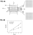
- the focal lengths provided by the field curvature corrector differ by approximately 8 ⁇ m between a central opening having a diameter of about 60 ⁇ m and an outer opening having a diameter of about 110 ⁇ m, when the second multi-aperture electrode 122 is grounded (U 2 grounded, see line marked with rectangles in FIG. 4B ).
- An increase of the second potential U 2 (and a decrease of the first potential U 1 ) leads to a reduced focal length variation ⁇ z between the central aperture and the outer apertures.
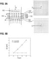
- the field curvature corrector 120 of FIG. 5A includes a first multi-aperture electrode 121 with a first plurality of openings providing a varying focal length on a plurality of beamlets, a second multi-aperture electrode 122 with a second plurality of openings aligned with the first plurality of openings, and an adjustment device 132 configured to adjust at least one of the first electrical potential U1 of the first multi-aperture electrode 121 and the second electrical potential U2 of the second multi-aperture electrode 122.
- a third multi-aperture electrode 123 with a third plurality of openings is provided.
- a fourth multi-aperture electrode 124 with a fourth plurality of openings is provided, wherein the third and fourth multi-aperture electrodes may be grounded.
- the diameters of the third plurality of openings may vary from the center to the outer regions in a way which is inverse to the variation of the diameters of the first plurality of openings from the center to the outer regions.
- the field curvature correction can be adjusted from a large correction (U1 high, U2 grounded) to zero correction (U2 high, U1 grounded).
- the field curvature correction is being achieved in a similar way as described above, and the varying diameters of the third multi-aperture electrode 123 have essentially no effect.
- the focal length variation introduced by the first multi-aperture electrode 121 is reduced, and in addition an inverse focal length variation is introduced by the third multi-aperture electrode 123. If the opening diameters are set properly, the net focal length for all beamlets of the plurality of beamlets is equal, resulting in no residual field curvature correction. Yet, the focal length provided by the field curvature corrector can be essentially kept constant when varying the first and second potentials as specified above.
- the field curvature correction can be set to "zero correction” by grounding the first multi-aperture electrode 121 (U 1 grounded) and setting the second multi-aperture on a potential >0 (U 2 high, e.g. 4kV or more). Yet, the intermediate image plane in which the field curvature corrector focuses can be kept essentially constant.
- the field curvature correction provided by a field curvature corrector 120 can be adjusted, e.g. when operating the charged particle beam device in different working modes.
- an intermediate image plane can be maintained at a constant position in different working modes of the charged particle beam device, such that the overall beam path does not substantially vary between the working modes.
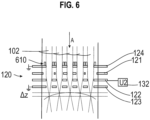
- the field curvature corrector 120 depicted in FIG. 6 further includes an electrostatic multipole device 610 including at least one multipole unit for each of the plurality of beamlets 102.
- the multipole units may be configured for at least one of aberration correction of the plurality of beamlets, deflection of the plurality of beamlets, or blanking of the plurality of beamlets.
- each of the plurality of beamlets may be deflected individually, such that the plurality of beamlets appear to come from different sources.
- spherical aberrations or higher order aberrations of the plurality of beamlets 102 may be individually compensated with the multipole units.
- a distance between a projection of the deflector electrodes on the optical axis and a projection of the corrector electrodes on the optical axis is smaller than the first length so that, during operation of the multipole device, first fringe fields generated by the deflector electrodes and second fringe fields generated by the corrector electrodes spatially overlap.
- the electrostatic corrector is configured to compensate for an aberration of the charged particle beam caused by the electrostatic deflector
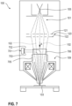
- FIG. 7 is a schematic sectional view of a charged particle beam device 100.
- the charged particle beam device 100 may be a scanning electron microscope in some embodiments.
- the charged particle beam device 100 includes a beam source 105, e.g. an electron source configured to generate a charged particle beam 101 propagating along an optical axis A, and a field curvature corrector 120 according to any of the embodiments described herein.
- the field curvature corrector 120 may be an adjustable field curvature corrector 120, such that the field curvature correction provided by the field curvature corrector 120 can be adjusted to the working mode of the charged particle beam device.
- the charged particle beam device 100 further includes beam influencing elements selected from the group consisting of a collimation lens, a transfer lens, an objective lens, an electrode, a multipole device, a deflector, and a scan deflector.
- beam influencing elements selected from the group consisting of a collimation lens, a transfer lens, an objective lens, an electrode, a multipole device, a deflector, and a scan deflector.
- the second electrical potential of the second multi-aperture electrode 122 of the field curvature corrector can be adjusted such that a first field curvature introduced by the field curvature corrector 120 is set inverse to a second field curvature caused by one or more of the beam influencing elements. Accordingly, the field curvature correction can be adapted to different working modes of the charged particle beam device.
- the charged particle beam device 100 further includes an objective lens system 109 figured to focus the plurality of beamlets 102 onto a specimen 103, and a segmented detector 701 configured to detect signal particles emitted from the specimen 103.
- the segmented detector 701 may include a plurality of detector segments configured to detect the signal particles generated upon impingement of the plurality of beamlets on the specimen.
- a first detector segment 702 and a second detector segment 703 are schematically depicted in FIG.
- first detector segment 702 is arranged to detect the signal particles generated by a first beamlet of the plurality of beamlets
- the second detector segment 703 is arranged to detect the signal particles generated by a second beamlet of the plurality of beamlets.
- a spatially resolved image can be generated, and/or the inspection speed can be increased by parallel inspection.
- the objective lens system 109 may include a combined magnetic-electrostatic objective lens including a magnetic lens portion and an electrostatic lens portion.
- a retarding field device may be provided which is configured to reduce the landing energy of the charged particles on the specimen.
- a retarding field electrode may be arranged upstream of the specimen.
- the beam source 105 is an electron source
- the charged particle beam is an electron beam
- the charged particle beam device 100 is a scanning electron microscope (SEM).
- the charged particle beam device 100 is another type of electron microscope.
- the charged particle beam device is an ion beam device, the beam source is an ion source, and the charged particle beam is an ion beam.
- a scanning electron microscope (SEM) as described herein is configured for imaging a specimen.
- the scanning electron microscope includes a beam source configured to generate a beam of electrons propagating along an optical axis, a field curvature corrector 120 as described herein, and a scan deflector 705 configured for scanning the plurality of beamlets 102 over the specimen 103.
- a field curvature corrector 120 for a multi-beam charged particle device 100 as described herein includes a first multi-aperture electrode 121 with a first plurality of openings for a plurality of beamlets of charged particles propagating next to each other, a second multi-aperture electrode 122 with a second plurality of openings for the plurality of beamlets, and an adjustment device 132 configured to adjust a second electrical potential U2 of the second multi-aperture electrode for adjusting a strength of a field curvature correction.
- an aperture device 110 with a plurality of openings to create the plurality of beamlets is arranged upstream of the field curvature corrector 120.
- the plurality of beamlets are created by the field curvature corrector 120, e.g. by one of the multi-aperture electrodes of the field curvature corrector.
- the first multi-aperture electrode 121, the second multi-aperture electrode 122, or another multi-aperture electrode of the field curvature corrector may be configured to create the plurality of beamlets from the charged particle beam.
- the first multi-aperture electrode 121 provides a focal length on the plurality of beamlets that varies with a distance D from an optical axis A, wherein the optical axis A is defined by a central opening of the field curvature corrector 120.
- a beamlet propagating close to the optical axis A through the first multi-aperture electrode device 121 is focused differently (i.e. with a different focal length) from a beamlet propagating distant from the optical axis A through the first multi-aperture device.
- the field curvature corrector 120 may include further features described herein, such that reference can be made to the above explanations.
- the field curvature corrector includes the third multi-aperture electrode 123 and the fourth multi-aperture electrode 124 as defined in the claims.
- a beam separator 706 is provided for separating the signal electrons which are emitted from the specimen from the electrons of the charged particle beam 101 propagating toward the specimen.
- the beam separator may for example be a magnetic beam separator or a Wien filter.
- FIG. 8 is a flow diagram illustrating a method of operating a charged particle beam device according to embodiments described herein.
- the method includes adjusting a field curvature corrector 120 to a first working mode of the charged particle beam device, and operating the charged particle beam device in the first working mode.
- the method includes adjusting the field curvature corrector to a second working mode of the charged particle beam device, and operating the charged particle beam device in the second working mode.
- the field curvature corrector 120 may include some or all of the features of any of the field curvature correctors described herein, such that reference can be made to the above explanations, which are not repeated here.
- a first field curvature of the plurality of beamlets that is compensated in the first working mode by the field curvature corrector 120 is different from a second field curvature of the plurality of beamlets that is compensated in the second wording mode by the field curvature corrector 120.
- a charged particle beam is generated which propagates along an optical axis A.
- a plurality of beamlets is created from the charged particle beam, particularly with an aperture device including a plurality of apertures.
- a field curvature is compensated with a field curvature corrector 120 as described herein.
- a second electrical potential of a second multi-aperture electrode 122 with a second plurality of openings arranged downstream of the first multi-aperture electrode 121 may be adjusted such that a field curvature in the plane of a specimen to be inspected is essentially zero. Accordingly, the foci of all the beamlets of the plurality of beamlets may lie in the plane of the specimen, such that a sharp image of the specimen can be provided in different working modes of the charged particle beam device.
Landscapes
- Chemical & Material Sciences (AREA)
- Analytical Chemistry (AREA)
- Electron Beam Exposure (AREA)
Claims (13)
- Correcteur de courbure de champ (120), comprenant :une première électrode à orifices multiples (121) avec une première pluralité d'ouvertures pour une pluralité de mini-faisceaux (102) de particules chargées se propageant les uns à côté des autres, la première pluralité d'ouvertures ayant des diamètres qui varient en tant que fonction d'une distance par rapport à l'axe optique (A) ;une deuxième électrode à orifices multiples (122) avec une deuxième pluralité d'ouvertures pour la pluralité de mini-faisceaux (102) ;une troisième électrode à orifices multiples (123) avec une troisième pluralité d'ouvertures en aval de la première électrode à orifices multiples (121) et de la deuxième électrode à orifices multiples (122), dans lequel la troisième pluralité d'ouvertures ont des diamètres qui varient en tant que seconde fonction de la distance par rapport à l'axe optique (A) ;une quatrième électrode à orifices multiples (124) avec une quatrième pluralité d'ouvertures en amont de la première électrode à orifices multiples (121) et de la deuxième électrode à orifices multiples (122) ; etun dispositif d'ajustement (132) configuré pour ajuster au moins l'un parmi un premier potentiel électrique (I11) de la première électrode à orifices multiples (121) et un second potentiel électrique (U2) de la deuxième électrode à orifices multiples (122),dans lequel les diamètres de la première pluralité d'ouvertures augmentent avec la distance par rapport à l'axe optique, et les diamètres de la troisième pluralité d'ouvertures diminuent avec la distance par rapport à l'axe optique, ou inversement.
- Dispositif de faisceau de particules chargées (100), comprenant :une source de faisceau (105) configurée pour générer un faisceau de particules chargées (101) se propageant le long d'un axe optique (A) ;un dispositif à orifices (110) avec une pluralité d'orifices configuré pour créer la pluralité de mini-faisceaux (102) à partir du faisceau de particules chargées (101) ; etle correcteur de courbure de champ (120) selon la revendication 1.
- Dispositif de faisceau de particules chargées (100) selon la revendication 2, dans lequel le dispositif d'ajustement (132) est configuré pour ajuster le premier potentiel électrique (U1) et le second potentiel électrique (U2).
- Dispositif de faisceau de particules chargées (100) selon la revendication 2 ou 3, dans lequel les diamètres de la première pluralité d'ouvertures augmentent avec la distance par rapport à l'axe optique, d'un premier diamètre de 80 µm ou moins à un second diamètre de 100 µm ou plus.
- Dispositif de faisceau de particules chargées (100) selon l'une quelconque des revendications 2 à 4, dans lequel la troisième électrode à orifices multiples (123) et la quatrième électrode à orifices multiples (124) sont reliées à la terre.
- Dispositif de faisceau de particules chargées (100) selon l'une quelconque des revendications 2 à 5, dans lequel la seconde fonction est sensiblement un inverse de la fonction.
- Dispositif de faisceau de particules chargées (100) selon l'une quelconque des revendications 2 à 6, comprenant en outre un ou plusieurs éléments influenceurs de faisceau choisis dans le groupe constitué par une lentille de collimation, une lentille de transfert, une lentille d'objectif, un dispositif multipolaire, un déflecteur et un déflecteur de balayage (705).
- Dispositif de faisceau de particules chargées (100) selon la revendication 7, dans lequel le second potentiel électrique est ajustable de telle sorte qu'une première courbure de champ introduite par le correcteur de courbure de champ (120) est sensiblement inverse à une seconde courbure de champ causée par le ou les éléments influenceurs de faisceau.
- Dispositif de faisceau de particules chargées (100) selon l'une quelconque des revendications 2 à 8, comprenant en outre dispositif électrostatique multipolaire (610) comprenant une unité multipolaire pour chacun parmi la pluralité de mini-faisceaux (102).
- Dispositif de faisceau de particules chargées (100) selon la revendication 9, dans lequel les unités multipolaires sont fournies au niveau d'une surface d'entrée de faisceau du correcteur de courbure de champ (120) ou au niveau d'une surface de sortie de faisceau du correcteur de courbure de champ (120).
- Dispositif de faisceau de particules chargées (100) selon l'une quelconque des revendications 2 à 10, comprenant en outre :un système de lentille d'objectif (109) configuré pour focaliser la pluralité de mini-faisceaux (102) sur un échantillon (103) ; etun détecteur segmenté configuré pour détecter des particules chargées de signal émises par l'échantillon (103).
- Dispositif de faisceau de particules chargées (100) selon l'une quelconque des revendications 2 à 11, dans lequel la source de faisceau (105) est une source d'électrons, le faisceau de particules chargées (101) est un faisceau d'électrons, et le dispositif de faisceau de particules chargées (100) est un microscope électronique à balayage.
- Procédé de fonctionnement d'un dispositif de faisceau de particules chargées (100), comprenant :la génération d'un faisceau de particules chargées (101) se propageant le long d'un axe optique ;la création d'une pluralité de mini-faisceaux (102) à partir du faisceau de particules chargées (101) ;la compensation d'une courbure de champ avec le correcteur de courbure de champ (120) selon la revendication 1, comprenant :la focalisation de la pluralité de mini-faisceaux (102) avec la première électrode à orifices multiples (121) du correcteur de courbure de champ ; etl'ajustement, avec le dispositif d'ajustement (132) du correcteur de courbure de champ (120), d'au moins l'un parmi le premier potentiel électrique et le second potentiel électrique ; etla focalisation de la pluralité de mini-faisceaux (102) sur un échantillon (103).
Applications Claiming Priority (2)
| Application Number | Priority Date | Filing Date | Title |
|---|---|---|---|
| US16/165,193 US10784070B2 (en) | 2018-10-19 | 2018-10-19 | Charged particle beam device, field curvature corrector, and methods of operating a charged particle beam device |
| PCT/EP2019/073465 WO2020078610A1 (fr) | 2018-10-19 | 2019-09-03 | Dispositif à faisceau de particules chargées, correcteur de courbure de champ, et procédés de fonctionnement du dispositif à faisceau de particules chargées |
Publications (2)
| Publication Number | Publication Date |
|---|---|
| EP3867941A1 EP3867941A1 (fr) | 2021-08-25 |
| EP3867941B1 true EP3867941B1 (fr) | 2025-01-29 |
Family
ID=67851129
Family Applications (1)
| Application Number | Title | Priority Date | Filing Date |
|---|---|---|---|
| EP19762955.3A Active EP3867941B1 (fr) | 2018-10-19 | 2019-09-03 | Correcteur de courbure de champ, dispositif à faisceau de particules chargées avec ce correcteur, et procédés de fonctionnement du dispositif à faisceau de particules chargées |
Country Status (6)
| Country | Link |
|---|---|
| US (1) | US10784070B2 (fr) |
| EP (1) | EP3867941B1 (fr) |
| KR (1) | KR102566320B1 (fr) |
| CN (1) | CN112840431A (fr) |
| TW (1) | TWI732305B (fr) |
| WO (1) | WO2020078610A1 (fr) |
Families Citing this family (19)
| Publication number | Priority date | Publication date | Assignee | Title |
|---|---|---|---|---|
| JP2021532545A (ja) * | 2018-08-09 | 2021-11-25 | エーエスエムエル ネザーランズ ビー.ブイ. | 複数の荷電粒子ビームのための装置 |
| JP7175798B2 (ja) * | 2019-03-01 | 2022-11-21 | 株式会社荏原製作所 | 荷電粒子マルチビーム装置 |
| CN111161998B (zh) * | 2020-02-10 | 2025-06-17 | 浙江迪谱诊断技术有限公司 | 一种激光同轴离子激发装置 |
| JP7547082B2 (ja) * | 2020-05-22 | 2024-09-09 | 株式会社ニューフレアテクノロジー | パターン検査装置及びパターン検査方法 |
| JP7474151B2 (ja) * | 2020-08-21 | 2024-04-24 | 株式会社ニューフレアテクノロジー | マルチ電子ビーム描画装置及びマルチ電子ビーム描画方法 |
| DE102021200799B3 (de) * | 2021-01-29 | 2022-03-31 | Carl Zeiss Multisem Gmbh | Verfahren mit verbesserter Fokuseinstellung unter Berücksichtigung eines Bildebenenkipps in einem Vielzahl-Teilchenstrahlmikroskop |
| EP4095881A1 (fr) * | 2021-05-25 | 2022-11-30 | ASML Netherlands B.V. | Dispositif de particules chargées |
| TW202312205A (zh) | 2021-05-27 | 2023-03-16 | 德商卡爾蔡司多重掃描電子顯微鏡有限公司 | 多重射束帶電粒子系統與在多重射束帶電粒子系統中控制工作距離的方法 |
| EP4102536A1 (fr) * | 2021-06-10 | 2022-12-14 | ASML Netherlands B.V. | Procédé de compensation d'un effet de distorsion d'électrode, système d'évaluation |
| US11651934B2 (en) * | 2021-09-30 | 2023-05-16 | Kla Corporation | Systems and methods of creating multiple electron beams |
| JP7080533B1 (ja) | 2021-11-09 | 2022-06-06 | 株式会社Photo electron Soul | 電子銃、電子線適用装置およびマルチ電子ビームの形成方法 |
| EP4432328A4 (fr) * | 2021-11-09 | 2025-11-05 | Photo Electron Soul Inc | Canon à électrons, dispositif d'application de faisceau d'électrons et procédé de formation de faisceau multi-électrons |
| CN119013755A (zh) * | 2022-04-12 | 2024-11-22 | 华为技术有限公司 | 一种粒子系统和粒子束的矫正方法 |
| WO2023197125A1 (fr) * | 2022-04-12 | 2023-10-19 | 华为技术有限公司 | Lentille électrostatique utilisée pour réduire la distance de défocalisation |
| JP2025514308A (ja) * | 2022-04-28 | 2025-05-02 | アプライド マテリアルズ インコーポレイテッド | パッケージング基板を試験するための方法およびパッケージング基板を試験するための装置 |
| US12525422B2 (en) * | 2022-08-08 | 2026-01-13 | Fei Company | Charged particle optics components and their fabrication |
| DE102023101774B4 (de) | 2023-01-25 | 2025-05-15 | Carl Zeiss Multisem Gmbh | Verfahren zum Auslegen eines Vielstrahl-Teilchenstrahlsystems mit monolithischen Bahnverlaufskorrekturplatten, Computerprogrammprodukt und Vielstrahl-Teilchenstrahlsystem |
| WO2024156469A1 (fr) | 2023-01-25 | 2024-08-02 | Carl Zeiss Multisem Gmbh | Microscope à particules à faisceaux multiples avec générateur à faisceaux multiples amélioré pour correction de courbure de champ et générateur à faisceaux multiples |
| CN116435163A (zh) * | 2023-06-12 | 2023-07-14 | 广东省科学院半导体研究所 | 多电子束场曲校正模块及电子束光柱体 |
Family Cites Families (12)
| Publication number | Priority date | Publication date | Assignee | Title |
|---|---|---|---|---|
| CN102709143B (zh) * | 2003-09-05 | 2016-03-09 | 卡尔蔡司Smt有限责任公司 | 电子光学排布结构、多电子分束检验系统和方法 |
| JP4359232B2 (ja) * | 2004-12-20 | 2009-11-04 | 株式会社日立ハイテクノロジーズ | 荷電粒子線装置 |
| JP5663717B2 (ja) | 2005-09-06 | 2015-02-04 | カール ツァイス マイクロスコピー ゲーエムベーハーCarl Zeiss Microscopy Gmbh | 荷電粒子システム |
| JP5159035B2 (ja) | 2005-10-28 | 2013-03-06 | キヤノン株式会社 | レンズアレイ及び該レンズアレイを含む荷電粒子線露光装置 |
| TWI593961B (zh) * | 2010-12-15 | 2017-08-01 | 日立全球先端科技股份有限公司 | Charged particle line application device, and irradiation method |
| JP5886663B2 (ja) | 2012-03-21 | 2016-03-16 | 株式会社日立ハイテクノロジーズ | 電子線応用装置およびレンズアレイ |
| JP2014007013A (ja) * | 2012-06-22 | 2014-01-16 | Canon Inc | 静電レンズアレイ、マルチ荷電粒子光学系、及びフォーカス調整方法 |
| JP6339734B2 (ja) * | 2015-02-18 | 2018-06-06 | 株式会社日立製作所 | 荷電粒子線応用装置、及び、収差補正器 |
| US9607805B2 (en) * | 2015-05-12 | 2017-03-28 | Hermes Microvision Inc. | Apparatus of plural charged-particle beams |
| US9620328B1 (en) * | 2015-11-20 | 2017-04-11 | ICT Integrated Circuit Testing Gesellschaft für Halbleiterprüftechnik mbH | Electrostatic multipole device, electrostatic multipole arrangement, charged particle beam device, and method of operating an electrostatic multipole device |
| US9922796B1 (en) * | 2016-12-01 | 2018-03-20 | Applied Materials Israel Ltd. | Method for inspecting a specimen and charged particle multi-beam device |
| US10453645B2 (en) * | 2016-12-01 | 2019-10-22 | Applied Materials Israel Ltd. | Method for inspecting a specimen and charged particle multi-beam device |
-
2018
- 2018-10-19 US US16/165,193 patent/US10784070B2/en active Active
-
2019
- 2019-09-03 EP EP19762955.3A patent/EP3867941B1/fr active Active
- 2019-09-03 CN CN201980067541.7A patent/CN112840431A/zh active Pending
- 2019-09-03 WO PCT/EP2019/073465 patent/WO2020078610A1/fr not_active Ceased
- 2019-09-03 KR KR1020217014998A patent/KR102566320B1/ko active Active
- 2019-10-03 TW TW108135826A patent/TWI732305B/zh active
Also Published As
| Publication number | Publication date |
|---|---|
| KR102566320B1 (ko) | 2023-08-16 |
| US20200126751A1 (en) | 2020-04-23 |
| TW202018751A (zh) | 2020-05-16 |
| US10784070B2 (en) | 2020-09-22 |
| CN112840431A (zh) | 2021-05-25 |
| TWI732305B (zh) | 2021-07-01 |
| EP3867941A1 (fr) | 2021-08-25 |
| WO2020078610A1 (fr) | 2020-04-23 |
| KR20210076117A (ko) | 2021-06-23 |
Similar Documents
| Publication | Publication Date | Title |
|---|---|---|
| EP3867941B1 (fr) | Correcteur de courbure de champ, dispositif à faisceau de particules chargées avec ce correcteur, et procédés de fonctionnement du dispositif à faisceau de particules chargées | |
| KR102214294B1 (ko) | 1차 하전 입자 빔렛들의 어레이를 이용한 시료의 검사를 위한 하전 입자 빔 디바이스 | |
| JP6728498B2 (ja) | 試験片を検査する方法および荷電粒子マルチビーム装置 | |
| US9922796B1 (en) | Method for inspecting a specimen and charged particle multi-beam device | |
| US10249472B2 (en) | Charged particle beam device, charged particle beam influencing device, and method of operating a charged particle beam device | |
| TWI755887B (zh) | 帶電粒子束裝置、操作帶電粒子束裝置的方法、及用於帶電粒子裝置的預補償器 | |
| CN115223831B (zh) | 带电粒子束设备、多子束组件和检查样本的方法 | |
| JP2003332207A (ja) | 電子ビーム露光装置及び電子ビーム処理装置 | |
| US20250191874A1 (en) | Optical system for a plurality of primary beamlets, charged particle multi-beam apparatus and method of focusing a plurality of primary beamlets |
Legal Events
| Date | Code | Title | Description |
|---|---|---|---|
| STAA | Information on the status of an ep patent application or granted ep patent |
Free format text: STATUS: UNKNOWN |
|
| STAA | Information on the status of an ep patent application or granted ep patent |
Free format text: STATUS: THE INTERNATIONAL PUBLICATION HAS BEEN MADE |
|
| PUAI | Public reference made under article 153(3) epc to a published international application that has entered the european phase |
Free format text: ORIGINAL CODE: 0009012 |
|
| STAA | Information on the status of an ep patent application or granted ep patent |
Free format text: STATUS: REQUEST FOR EXAMINATION WAS MADE |
|
| 17P | Request for examination filed |
Effective date: 20210318 |
|
| AK | Designated contracting states |
Kind code of ref document: A1 Designated state(s): AL AT BE BG CH CY CZ DE DK EE ES FI FR GB GR HR HU IE IS IT LI LT LU LV MC MK MT NL NO PL PT RO RS SE SI SK SM TR |
|
| DAV | Request for validation of the european patent (deleted) | ||
| DAX | Request for extension of the european patent (deleted) | ||
| STAA | Information on the status of an ep patent application or granted ep patent |
Free format text: STATUS: EXAMINATION IS IN PROGRESS |
|
| 17Q | First examination report despatched |
Effective date: 20240730 |
|
| GRAP | Despatch of communication of intention to grant a patent |
Free format text: ORIGINAL CODE: EPIDOSNIGR1 |
|
| STAA | Information on the status of an ep patent application or granted ep patent |
Free format text: STATUS: GRANT OF PATENT IS INTENDED |
|
| INTG | Intention to grant announced |
Effective date: 20241010 |
|
| P01 | Opt-out of the competence of the unified patent court (upc) registered |
Free format text: CASE NUMBER: APP_59564/2024 Effective date: 20241104 |
|
| GRAS | Grant fee paid |
Free format text: ORIGINAL CODE: EPIDOSNIGR3 |
|
| GRAA | (expected) grant |
Free format text: ORIGINAL CODE: 0009210 |
|
| STAA | Information on the status of an ep patent application or granted ep patent |
Free format text: STATUS: THE PATENT HAS BEEN GRANTED |
|
| AK | Designated contracting states |
Kind code of ref document: B1 Designated state(s): AL AT BE BG CH CY CZ DE DK EE ES FI FR GB GR HR HU IE IS IT LI LT LU LV MC MK MT NL NO PL PT RO RS SE SI SK SM TR |
|
| REG | Reference to a national code |
Ref country code: GB Ref legal event code: FG4D |
|
| REG | Reference to a national code |
Ref country code: CH Ref legal event code: EP |
|
| REG | Reference to a national code |
Ref country code: DE Ref legal event code: R096 Ref document number: 602019065414 Country of ref document: DE |
|
| REG | Reference to a national code |
Ref country code: IE Ref legal event code: FG4D |
|
| REG | Reference to a national code |
Ref country code: NL Ref legal event code: FP |
|
| PG25 | Lapsed in a contracting state [announced via postgrant information from national office to epo] |
Ref country code: RS Free format text: LAPSE BECAUSE OF FAILURE TO SUBMIT A TRANSLATION OF THE DESCRIPTION OR TO PAY THE FEE WITHIN THE PRESCRIBED TIME-LIMIT Effective date: 20250429 |
|
| PG25 | Lapsed in a contracting state [announced via postgrant information from national office to epo] |
Ref country code: FI Free format text: LAPSE BECAUSE OF FAILURE TO SUBMIT A TRANSLATION OF THE DESCRIPTION OR TO PAY THE FEE WITHIN THE PRESCRIBED TIME-LIMIT Effective date: 20250129 |
|
| PG25 | Lapsed in a contracting state [announced via postgrant information from national office to epo] |
Ref country code: PL Free format text: LAPSE BECAUSE OF FAILURE TO SUBMIT A TRANSLATION OF THE DESCRIPTION OR TO PAY THE FEE WITHIN THE PRESCRIBED TIME-LIMIT Effective date: 20250129 |
|
| PG25 | Lapsed in a contracting state [announced via postgrant information from national office to epo] |
Ref country code: ES Free format text: LAPSE BECAUSE OF FAILURE TO SUBMIT A TRANSLATION OF THE DESCRIPTION OR TO PAY THE FEE WITHIN THE PRESCRIBED TIME-LIMIT Effective date: 20250129 |
|
| REG | Reference to a national code |
Ref country code: LT Ref legal event code: MG9D |
|
| PG25 | Lapsed in a contracting state [announced via postgrant information from national office to epo] |
Ref country code: NO Free format text: LAPSE BECAUSE OF FAILURE TO SUBMIT A TRANSLATION OF THE DESCRIPTION OR TO PAY THE FEE WITHIN THE PRESCRIBED TIME-LIMIT Effective date: 20250429 Ref country code: IS Free format text: LAPSE BECAUSE OF FAILURE TO SUBMIT A TRANSLATION OF THE DESCRIPTION OR TO PAY THE FEE WITHIN THE PRESCRIBED TIME-LIMIT Effective date: 20250529 |
|
| REG | Reference to a national code |
Ref country code: AT Ref legal event code: MK05 Ref document number: 1764334 Country of ref document: AT Kind code of ref document: T Effective date: 20250129 |
|
| PG25 | Lapsed in a contracting state [announced via postgrant information from national office to epo] |
Ref country code: HR Free format text: LAPSE BECAUSE OF FAILURE TO SUBMIT A TRANSLATION OF THE DESCRIPTION OR TO PAY THE FEE WITHIN THE PRESCRIBED TIME-LIMIT Effective date: 20250129 |
|
| PG25 | Lapsed in a contracting state [announced via postgrant information from national office to epo] |
Ref country code: LV Free format text: LAPSE BECAUSE OF FAILURE TO SUBMIT A TRANSLATION OF THE DESCRIPTION OR TO PAY THE FEE WITHIN THE PRESCRIBED TIME-LIMIT Effective date: 20250129 Ref country code: PT Free format text: LAPSE BECAUSE OF FAILURE TO SUBMIT A TRANSLATION OF THE DESCRIPTION OR TO PAY THE FEE WITHIN THE PRESCRIBED TIME-LIMIT Effective date: 20250529 |
|
| PG25 | Lapsed in a contracting state [announced via postgrant information from national office to epo] |
Ref country code: GR Free format text: LAPSE BECAUSE OF FAILURE TO SUBMIT A TRANSLATION OF THE DESCRIPTION OR TO PAY THE FEE WITHIN THE PRESCRIBED TIME-LIMIT Effective date: 20250430 Ref country code: BG Free format text: LAPSE BECAUSE OF FAILURE TO SUBMIT A TRANSLATION OF THE DESCRIPTION OR TO PAY THE FEE WITHIN THE PRESCRIBED TIME-LIMIT Effective date: 20250129 |
|
| PG25 | Lapsed in a contracting state [announced via postgrant information from national office to epo] |
Ref country code: AT Free format text: LAPSE BECAUSE OF FAILURE TO SUBMIT A TRANSLATION OF THE DESCRIPTION OR TO PAY THE FEE WITHIN THE PRESCRIBED TIME-LIMIT Effective date: 20250129 |
|
| PG25 | Lapsed in a contracting state [announced via postgrant information from national office to epo] |
Ref country code: SE Free format text: LAPSE BECAUSE OF FAILURE TO SUBMIT A TRANSLATION OF THE DESCRIPTION OR TO PAY THE FEE WITHIN THE PRESCRIBED TIME-LIMIT Effective date: 20250129 |
|
| PGFP | Annual fee paid to national office [announced via postgrant information from national office to epo] |
Ref country code: NL Payment date: 20250820 Year of fee payment: 7 |
|
| PG25 | Lapsed in a contracting state [announced via postgrant information from national office to epo] |
Ref country code: SM Free format text: LAPSE BECAUSE OF FAILURE TO SUBMIT A TRANSLATION OF THE DESCRIPTION OR TO PAY THE FEE WITHIN THE PRESCRIBED TIME-LIMIT Effective date: 20250129 |
|
| PG25 | Lapsed in a contracting state [announced via postgrant information from national office to epo] |
Ref country code: DK Free format text: LAPSE BECAUSE OF FAILURE TO SUBMIT A TRANSLATION OF THE DESCRIPTION OR TO PAY THE FEE WITHIN THE PRESCRIBED TIME-LIMIT Effective date: 20250129 |
|
| PGFP | Annual fee paid to national office [announced via postgrant information from national office to epo] |
Ref country code: DE Payment date: 20250820 Year of fee payment: 7 |
|
| PG25 | Lapsed in a contracting state [announced via postgrant information from national office to epo] |
Ref country code: IT Free format text: LAPSE BECAUSE OF FAILURE TO SUBMIT A TRANSLATION OF THE DESCRIPTION OR TO PAY THE FEE WITHIN THE PRESCRIBED TIME-LIMIT Effective date: 20250129 |
|
| PG25 | Lapsed in a contracting state [announced via postgrant information from national office to epo] |
Ref country code: CZ Free format text: LAPSE BECAUSE OF FAILURE TO SUBMIT A TRANSLATION OF THE DESCRIPTION OR TO PAY THE FEE WITHIN THE PRESCRIBED TIME-LIMIT Effective date: 20250129 Ref country code: EE Free format text: LAPSE BECAUSE OF FAILURE TO SUBMIT A TRANSLATION OF THE DESCRIPTION OR TO PAY THE FEE WITHIN THE PRESCRIBED TIME-LIMIT Effective date: 20250129 |
|
| PG25 | Lapsed in a contracting state [announced via postgrant information from national office to epo] |
Ref country code: RO Free format text: LAPSE BECAUSE OF FAILURE TO SUBMIT A TRANSLATION OF THE DESCRIPTION OR TO PAY THE FEE WITHIN THE PRESCRIBED TIME-LIMIT Effective date: 20250129 |
|
| PG25 | Lapsed in a contracting state [announced via postgrant information from national office to epo] |
Ref country code: SK Free format text: LAPSE BECAUSE OF FAILURE TO SUBMIT A TRANSLATION OF THE DESCRIPTION OR TO PAY THE FEE WITHIN THE PRESCRIBED TIME-LIMIT Effective date: 20250129 |
|
| REG | Reference to a national code |
Ref country code: DE Ref legal event code: R097 Ref document number: 602019065414 Country of ref document: DE |
|
| PLBE | No opposition filed within time limit |
Free format text: ORIGINAL CODE: 0009261 |
|
| STAA | Information on the status of an ep patent application or granted ep patent |
Free format text: STATUS: NO OPPOSITION FILED WITHIN TIME LIMIT |
|
| REG | Reference to a national code |
Ref country code: CH Ref legal event code: L10 Free format text: ST27 STATUS EVENT CODE: U-0-0-L10-L00 (AS PROVIDED BY THE NATIONAL OFFICE) Effective date: 20251210 |
|
| 26N | No opposition filed |
Effective date: 20251030 |
|
| REG | Reference to a national code |
Ref country code: CH Ref legal event code: H13 Free format text: ST27 STATUS EVENT CODE: U-0-0-H10-H13 (AS PROVIDED BY THE NATIONAL OFFICE) Effective date: 20260425 |