EP3868502B1 - Outil de coupe - Google Patents
Outil de coupe Download PDFInfo
- Publication number
- EP3868502B1 EP3868502B1 EP19873707.4A EP19873707A EP3868502B1 EP 3868502 B1 EP3868502 B1 EP 3868502B1 EP 19873707 A EP19873707 A EP 19873707A EP 3868502 B1 EP3868502 B1 EP 3868502B1
- Authority
- EP
- European Patent Office
- Prior art keywords
- layer
- residual stress
- substrate
- equal
- mpa
- Prior art date
- Legal status (The legal status is an assumption and is not a legal conclusion. Google has not performed a legal analysis and makes no representation as to the accuracy of the status listed.)
- Active
Links
Images


Classifications
-
- B—PERFORMING OPERATIONS; TRANSPORTING
- B23—MACHINE TOOLS; METAL-WORKING NOT OTHERWISE PROVIDED FOR
- B23B—TURNING; BORING
- B23B27/00—Tools for turning or boring machines; Tools of a similar kind in general; Accessories therefor
- B23B27/14—Cutting tools of which the bits or tips or cutting inserts are of special material
-
- B—PERFORMING OPERATIONS; TRANSPORTING
- B23—MACHINE TOOLS; METAL-WORKING NOT OTHERWISE PROVIDED FOR
- B23B—TURNING; BORING
- B23B51/00—Tools for drilling machines
-
- B—PERFORMING OPERATIONS; TRANSPORTING
- B23—MACHINE TOOLS; METAL-WORKING NOT OTHERWISE PROVIDED FOR
- B23C—MILLING
- B23C5/00—Milling-cutters
- B23C5/16—Milling-cutters characterised by physical features other than shape
-
- C—CHEMISTRY; METALLURGY
- C23—COATING METALLIC MATERIAL; COATING MATERIAL WITH METALLIC MATERIAL; CHEMICAL SURFACE TREATMENT; DIFFUSION TREATMENT OF METALLIC MATERIAL; COATING BY VACUUM EVAPORATION, BY SPUTTERING, BY ION IMPLANTATION OR BY CHEMICAL VAPOUR DEPOSITION, IN GENERAL; INHIBITING CORROSION OF METALLIC MATERIAL OR INCRUSTATION IN GENERAL
- C23C—COATING METALLIC MATERIAL; COATING MATERIAL WITH METALLIC MATERIAL; SURFACE TREATMENT OF METALLIC MATERIAL BY DIFFUSION INTO THE SURFACE, BY CHEMICAL CONVERSION OR SUBSTITUTION; COATING BY VACUUM EVAPORATION, BY SPUTTERING, BY ION IMPLANTATION OR BY CHEMICAL VAPOUR DEPOSITION, IN GENERAL
- C23C14/00—Coating by vacuum evaporation, by sputtering or by ion implantation of the coating forming material
- C23C14/06—Coating by vacuum evaporation, by sputtering or by ion implantation of the coating forming material characterised by the coating material
- C23C14/08—Oxides
-
- C—CHEMISTRY; METALLURGY
- C23—COATING METALLIC MATERIAL; COATING MATERIAL WITH METALLIC MATERIAL; CHEMICAL SURFACE TREATMENT; DIFFUSION TREATMENT OF METALLIC MATERIAL; COATING BY VACUUM EVAPORATION, BY SPUTTERING, BY ION IMPLANTATION OR BY CHEMICAL VAPOUR DEPOSITION, IN GENERAL; INHIBITING CORROSION OF METALLIC MATERIAL OR INCRUSTATION IN GENERAL
- C23C—COATING METALLIC MATERIAL; COATING MATERIAL WITH METALLIC MATERIAL; SURFACE TREATMENT OF METALLIC MATERIAL BY DIFFUSION INTO THE SURFACE, BY CHEMICAL CONVERSION OR SUBSTITUTION; COATING BY VACUUM EVAPORATION, BY SPUTTERING, BY ION IMPLANTATION OR BY CHEMICAL VAPOUR DEPOSITION, IN GENERAL
- C23C16/00—Chemical coating by decomposition of gaseous compounds, without leaving reaction products of surface material in the coating, i.e. chemical vapour deposition [CVD] processes
- C23C16/02—Pretreatment of the material to be coated
- C23C16/0272—Deposition of sub-layers, e.g. to promote the adhesion of the main coating
-
- C—CHEMISTRY; METALLURGY
- C23—COATING METALLIC MATERIAL; COATING MATERIAL WITH METALLIC MATERIAL; CHEMICAL SURFACE TREATMENT; DIFFUSION TREATMENT OF METALLIC MATERIAL; COATING BY VACUUM EVAPORATION, BY SPUTTERING, BY ION IMPLANTATION OR BY CHEMICAL VAPOUR DEPOSITION, IN GENERAL; INHIBITING CORROSION OF METALLIC MATERIAL OR INCRUSTATION IN GENERAL
- C23C—COATING METALLIC MATERIAL; COATING MATERIAL WITH METALLIC MATERIAL; SURFACE TREATMENT OF METALLIC MATERIAL BY DIFFUSION INTO THE SURFACE, BY CHEMICAL CONVERSION OR SUBSTITUTION; COATING BY VACUUM EVAPORATION, BY SPUTTERING, BY ION IMPLANTATION OR BY CHEMICAL VAPOUR DEPOSITION, IN GENERAL
- C23C16/00—Chemical coating by decomposition of gaseous compounds, without leaving reaction products of surface material in the coating, i.e. chemical vapour deposition [CVD] processes
- C23C16/22—Chemical coating by decomposition of gaseous compounds, without leaving reaction products of surface material in the coating, i.e. chemical vapour deposition [CVD] processes characterised by the deposition of inorganic material, other than metallic material
- C23C16/30—Deposition of compounds, mixtures or solid solutions, e.g. borides, carbides, nitrides
- C23C16/36—Carbonitrides
-
- C—CHEMISTRY; METALLURGY
- C23—COATING METALLIC MATERIAL; COATING MATERIAL WITH METALLIC MATERIAL; CHEMICAL SURFACE TREATMENT; DIFFUSION TREATMENT OF METALLIC MATERIAL; COATING BY VACUUM EVAPORATION, BY SPUTTERING, BY ION IMPLANTATION OR BY CHEMICAL VAPOUR DEPOSITION, IN GENERAL; INHIBITING CORROSION OF METALLIC MATERIAL OR INCRUSTATION IN GENERAL
- C23C—COATING METALLIC MATERIAL; COATING MATERIAL WITH METALLIC MATERIAL; SURFACE TREATMENT OF METALLIC MATERIAL BY DIFFUSION INTO THE SURFACE, BY CHEMICAL CONVERSION OR SUBSTITUTION; COATING BY VACUUM EVAPORATION, BY SPUTTERING, BY ION IMPLANTATION OR BY CHEMICAL VAPOUR DEPOSITION, IN GENERAL
- C23C16/00—Chemical coating by decomposition of gaseous compounds, without leaving reaction products of surface material in the coating, i.e. chemical vapour deposition [CVD] processes
- C23C16/22—Chemical coating by decomposition of gaseous compounds, without leaving reaction products of surface material in the coating, i.e. chemical vapour deposition [CVD] processes characterised by the deposition of inorganic material, other than metallic material
- C23C16/30—Deposition of compounds, mixtures or solid solutions, e.g. borides, carbides, nitrides
- C23C16/40—Oxides
-
- C—CHEMISTRY; METALLURGY
- C23—COATING METALLIC MATERIAL; COATING MATERIAL WITH METALLIC MATERIAL; CHEMICAL SURFACE TREATMENT; DIFFUSION TREATMENT OF METALLIC MATERIAL; COATING BY VACUUM EVAPORATION, BY SPUTTERING, BY ION IMPLANTATION OR BY CHEMICAL VAPOUR DEPOSITION, IN GENERAL; INHIBITING CORROSION OF METALLIC MATERIAL OR INCRUSTATION IN GENERAL
- C23C—COATING METALLIC MATERIAL; COATING MATERIAL WITH METALLIC MATERIAL; SURFACE TREATMENT OF METALLIC MATERIAL BY DIFFUSION INTO THE SURFACE, BY CHEMICAL CONVERSION OR SUBSTITUTION; COATING BY VACUUM EVAPORATION, BY SPUTTERING, BY ION IMPLANTATION OR BY CHEMICAL VAPOUR DEPOSITION, IN GENERAL
- C23C16/00—Chemical coating by decomposition of gaseous compounds, without leaving reaction products of surface material in the coating, i.e. chemical vapour deposition [CVD] processes
- C23C16/22—Chemical coating by decomposition of gaseous compounds, without leaving reaction products of surface material in the coating, i.e. chemical vapour deposition [CVD] processes characterised by the deposition of inorganic material, other than metallic material
- C23C16/30—Deposition of compounds, mixtures or solid solutions, e.g. borides, carbides, nitrides
- C23C16/40—Oxides
- C23C16/403—Oxides of aluminium, magnesium or beryllium
-
- C—CHEMISTRY; METALLURGY
- C23—COATING METALLIC MATERIAL; COATING MATERIAL WITH METALLIC MATERIAL; CHEMICAL SURFACE TREATMENT; DIFFUSION TREATMENT OF METALLIC MATERIAL; COATING BY VACUUM EVAPORATION, BY SPUTTERING, BY ION IMPLANTATION OR BY CHEMICAL VAPOUR DEPOSITION, IN GENERAL; INHIBITING CORROSION OF METALLIC MATERIAL OR INCRUSTATION IN GENERAL
- C23C—COATING METALLIC MATERIAL; COATING MATERIAL WITH METALLIC MATERIAL; SURFACE TREATMENT OF METALLIC MATERIAL BY DIFFUSION INTO THE SURFACE, BY CHEMICAL CONVERSION OR SUBSTITUTION; COATING BY VACUUM EVAPORATION, BY SPUTTERING, BY ION IMPLANTATION OR BY CHEMICAL VAPOUR DEPOSITION, IN GENERAL
- C23C16/00—Chemical coating by decomposition of gaseous compounds, without leaving reaction products of surface material in the coating, i.e. chemical vapour deposition [CVD] processes
- C23C16/44—Chemical coating by decomposition of gaseous compounds, without leaving reaction products of surface material in the coating, i.e. chemical vapour deposition [CVD] processes characterised by the method of coating
- C23C16/455—Chemical coating by decomposition of gaseous compounds, without leaving reaction products of surface material in the coating, i.e. chemical vapour deposition [CVD] processes characterised by the method of coating characterised by the method used for introducing gases into reaction chamber or for modifying gas flows in reaction chamber
- C23C16/45502—Flow conditions in reaction chamber
- C23C16/45508—Radial flow
-
- C—CHEMISTRY; METALLURGY
- C23—COATING METALLIC MATERIAL; COATING MATERIAL WITH METALLIC MATERIAL; CHEMICAL SURFACE TREATMENT; DIFFUSION TREATMENT OF METALLIC MATERIAL; COATING BY VACUUM EVAPORATION, BY SPUTTERING, BY ION IMPLANTATION OR BY CHEMICAL VAPOUR DEPOSITION, IN GENERAL; INHIBITING CORROSION OF METALLIC MATERIAL OR INCRUSTATION IN GENERAL
- C23C—COATING METALLIC MATERIAL; COATING MATERIAL WITH METALLIC MATERIAL; SURFACE TREATMENT OF METALLIC MATERIAL BY DIFFUSION INTO THE SURFACE, BY CHEMICAL CONVERSION OR SUBSTITUTION; COATING BY VACUUM EVAPORATION, BY SPUTTERING, BY ION IMPLANTATION OR BY CHEMICAL VAPOUR DEPOSITION, IN GENERAL
- C23C16/00—Chemical coating by decomposition of gaseous compounds, without leaving reaction products of surface material in the coating, i.e. chemical vapour deposition [CVD] processes
- C23C16/44—Chemical coating by decomposition of gaseous compounds, without leaving reaction products of surface material in the coating, i.e. chemical vapour deposition [CVD] processes characterised by the method of coating
- C23C16/455—Chemical coating by decomposition of gaseous compounds, without leaving reaction products of surface material in the coating, i.e. chemical vapour deposition [CVD] processes characterised by the method of coating characterised by the method used for introducing gases into reaction chamber or for modifying gas flows in reaction chamber
- C23C16/45563—Gas nozzles
- C23C16/45578—Elongated nozzles, tubes with holes
-
- C—CHEMISTRY; METALLURGY
- C23—COATING METALLIC MATERIAL; COATING MATERIAL WITH METALLIC MATERIAL; CHEMICAL SURFACE TREATMENT; DIFFUSION TREATMENT OF METALLIC MATERIAL; COATING BY VACUUM EVAPORATION, BY SPUTTERING, BY ION IMPLANTATION OR BY CHEMICAL VAPOUR DEPOSITION, IN GENERAL; INHIBITING CORROSION OF METALLIC MATERIAL OR INCRUSTATION IN GENERAL
- C23C—COATING METALLIC MATERIAL; COATING MATERIAL WITH METALLIC MATERIAL; SURFACE TREATMENT OF METALLIC MATERIAL BY DIFFUSION INTO THE SURFACE, BY CHEMICAL CONVERSION OR SUBSTITUTION; COATING BY VACUUM EVAPORATION, BY SPUTTERING, BY ION IMPLANTATION OR BY CHEMICAL VAPOUR DEPOSITION, IN GENERAL
- C23C16/00—Chemical coating by decomposition of gaseous compounds, without leaving reaction products of surface material in the coating, i.e. chemical vapour deposition [CVD] processes
- C23C16/56—After-treatment
-
- C—CHEMISTRY; METALLURGY
- C23—COATING METALLIC MATERIAL; COATING MATERIAL WITH METALLIC MATERIAL; CHEMICAL SURFACE TREATMENT; DIFFUSION TREATMENT OF METALLIC MATERIAL; COATING BY VACUUM EVAPORATION, BY SPUTTERING, BY ION IMPLANTATION OR BY CHEMICAL VAPOUR DEPOSITION, IN GENERAL; INHIBITING CORROSION OF METALLIC MATERIAL OR INCRUSTATION IN GENERAL
- C23C—COATING METALLIC MATERIAL; COATING MATERIAL WITH METALLIC MATERIAL; SURFACE TREATMENT OF METALLIC MATERIAL BY DIFFUSION INTO THE SURFACE, BY CHEMICAL CONVERSION OR SUBSTITUTION; COATING BY VACUUM EVAPORATION, BY SPUTTERING, BY ION IMPLANTATION OR BY CHEMICAL VAPOUR DEPOSITION, IN GENERAL
- C23C28/00—Coating for obtaining at least two superposed coatings either by methods not provided for in a single one of groups C23C2/00 - C23C26/00 or by combinations of methods provided for in subclasses C23C and C25C or C25D
- C23C28/04—Coating for obtaining at least two superposed coatings either by methods not provided for in a single one of groups C23C2/00 - C23C26/00 or by combinations of methods provided for in subclasses C23C and C25C or C25D only coatings of inorganic non-metallic material
- C23C28/044—Coating for obtaining at least two superposed coatings either by methods not provided for in a single one of groups C23C2/00 - C23C26/00 or by combinations of methods provided for in subclasses C23C and C25C or C25D only coatings of inorganic non-metallic material coatings specially adapted for cutting tools or wear applications
-
- C—CHEMISTRY; METALLURGY
- C23—COATING METALLIC MATERIAL; COATING MATERIAL WITH METALLIC MATERIAL; CHEMICAL SURFACE TREATMENT; DIFFUSION TREATMENT OF METALLIC MATERIAL; COATING BY VACUUM EVAPORATION, BY SPUTTERING, BY ION IMPLANTATION OR BY CHEMICAL VAPOUR DEPOSITION, IN GENERAL; INHIBITING CORROSION OF METALLIC MATERIAL OR INCRUSTATION IN GENERAL
- C23C—COATING METALLIC MATERIAL; COATING MATERIAL WITH METALLIC MATERIAL; SURFACE TREATMENT OF METALLIC MATERIAL BY DIFFUSION INTO THE SURFACE, BY CHEMICAL CONVERSION OR SUBSTITUTION; COATING BY VACUUM EVAPORATION, BY SPUTTERING, BY ION IMPLANTATION OR BY CHEMICAL VAPOUR DEPOSITION, IN GENERAL
- C23C28/00—Coating for obtaining at least two superposed coatings either by methods not provided for in a single one of groups C23C2/00 - C23C26/00 or by combinations of methods provided for in subclasses C23C and C25C or C25D
- C23C28/04—Coating for obtaining at least two superposed coatings either by methods not provided for in a single one of groups C23C2/00 - C23C26/00 or by combinations of methods provided for in subclasses C23C and C25C or C25D only coatings of inorganic non-metallic material
- C23C28/048—Coating for obtaining at least two superposed coatings either by methods not provided for in a single one of groups C23C2/00 - C23C26/00 or by combinations of methods provided for in subclasses C23C and C25C or C25D only coatings of inorganic non-metallic material with layers graded in composition or physical properties
-
- C—CHEMISTRY; METALLURGY
- C23—COATING METALLIC MATERIAL; COATING MATERIAL WITH METALLIC MATERIAL; CHEMICAL SURFACE TREATMENT; DIFFUSION TREATMENT OF METALLIC MATERIAL; COATING BY VACUUM EVAPORATION, BY SPUTTERING, BY ION IMPLANTATION OR BY CHEMICAL VAPOUR DEPOSITION, IN GENERAL; INHIBITING CORROSION OF METALLIC MATERIAL OR INCRUSTATION IN GENERAL
- C23C—COATING METALLIC MATERIAL; COATING MATERIAL WITH METALLIC MATERIAL; SURFACE TREATMENT OF METALLIC MATERIAL BY DIFFUSION INTO THE SURFACE, BY CHEMICAL CONVERSION OR SUBSTITUTION; COATING BY VACUUM EVAPORATION, BY SPUTTERING, BY ION IMPLANTATION OR BY CHEMICAL VAPOUR DEPOSITION, IN GENERAL
- C23C28/00—Coating for obtaining at least two superposed coatings either by methods not provided for in a single one of groups C23C2/00 - C23C26/00 or by combinations of methods provided for in subclasses C23C and C25C or C25D
- C23C28/30—Coatings combining at least one metallic layer and at least one inorganic non-metallic layer
- C23C28/34—Coatings combining at least one metallic layer and at least one inorganic non-metallic layer including at least one inorganic non-metallic material layer, e.g. metal carbide, nitride, boride, silicide layer and their mixtures, enamels, phosphates and sulphates
- C23C28/345—Coatings combining at least one metallic layer and at least one inorganic non-metallic layer including at least one inorganic non-metallic material layer, e.g. metal carbide, nitride, boride, silicide layer and their mixtures, enamels, phosphates and sulphates with at least one oxide layer
- C23C28/3455—Coatings combining at least one metallic layer and at least one inorganic non-metallic layer including at least one inorganic non-metallic material layer, e.g. metal carbide, nitride, boride, silicide layer and their mixtures, enamels, phosphates and sulphates with at least one oxide layer with a refractory ceramic layer, e.g. refractory metal oxide, ZrO2, rare earth oxides or a thermal barrier system comprising at least one refractory oxide layer
-
- C—CHEMISTRY; METALLURGY
- C23—COATING METALLIC MATERIAL; COATING MATERIAL WITH METALLIC MATERIAL; CHEMICAL SURFACE TREATMENT; DIFFUSION TREATMENT OF METALLIC MATERIAL; COATING BY VACUUM EVAPORATION, BY SPUTTERING, BY ION IMPLANTATION OR BY CHEMICAL VAPOUR DEPOSITION, IN GENERAL; INHIBITING CORROSION OF METALLIC MATERIAL OR INCRUSTATION IN GENERAL
- C23C—COATING METALLIC MATERIAL; COATING MATERIAL WITH METALLIC MATERIAL; SURFACE TREATMENT OF METALLIC MATERIAL BY DIFFUSION INTO THE SURFACE, BY CHEMICAL CONVERSION OR SUBSTITUTION; COATING BY VACUUM EVAPORATION, BY SPUTTERING, BY ION IMPLANTATION OR BY CHEMICAL VAPOUR DEPOSITION, IN GENERAL
- C23C30/00—Coating with metallic material characterised only by the composition of the metallic material, i.e. not characterised by the coating process
- C23C30/005—Coating with metallic material characterised only by the composition of the metallic material, i.e. not characterised by the coating process on hard metal substrates
Definitions
- the present invention relates to a coated cutting tool.
- the present application claims a priority based on Japanese Patent Application No. 2018-194134 filed on October 15, 2018 .
- Patent Literature 1 discloses a surface-coated cutting tool having a coating film including an ⁇ -Al 2 O 3 layer in which a total area of crystal grains exhibiting a crystal orientation of a (0001) plane is more than or equal to 70% when seen in a plan view in the normal direction of a surface of the layer.
- Patent Literature 2 discloses a coated cutting tool having a cemented carbide body and a coating, wherein at least an outermost layer of the coating is an ⁇ -Al 2 O 3 layer that has a thickness of 7 to 12 ⁇ m and that is oriented in a (006) direction, an orientation coefficient TC (006) thereof is more than 2 and less than 6, each of orientation coefficients TC (012), TC (110), TC (113), TC (202), TC (024) and TC (116) is less than 1, and an orientation coefficient TC (104) is the second largest orientation coefficient.
- JP 2017 042901 A and JP 2017 042902 A disclose coated cutting tools comprising an ⁇ -Al 2 O 3 layer in which the residual stresses in the alumina layer at the outermost surface are compressive stresses.
- a cutting tool according to the present invention is a cutting tool according to claim including: a substrate including a rake face; and a coating film that coats the rake face, wherein
- Patent Literature 1 and Patent Literature 2 since the coating film having the ⁇ -Al 2 O 3 layer configured as described above is included, mechanical characteristics of the surface-coated cutting tool, such as wear resistance (for example, crater wear resistance or the like) and breakage resistance, are improved, with the result that the life of the cutting tool is expected to be long.
- wear resistance for example, crater wear resistance or the like
- breakage resistance breakage resistance
- the present disclosure has been made in view of the above-described circumstances, and has an object to provide a cutting tool excellent in chipping resistance and crater wear resistance.
- a cutting tool excellent in chipping resistance and crater wear resistance can be provided.
- a cutting tool according to the present invention is a cutting tool including: a substrate including a rake face; and a coating film that coats the rake face, wherein
- the cutting tool can have an excellent chipping resistance and an excellent crater wear resistance.
- the term “chipping resistance” refers to a characteristic of suppressing breakage or detachment of only a surface layer of the coating film.
- the inventive ⁇ -Al 2 O 3 layer has a thickness of more than or equal to 1 ⁇ m and less than or equal to 20 ⁇ m,
- a stress distribution of the residual stress A has
- a stress distribution of the residual stress B has
- the coating film further includes one or more intermediate layers disposed between the substrate and the ⁇ -Al 2 O 3 layer, and each of the intermediate layers includes a compound that is composed of at least one element selected from a group consisting of a group 4 element, a group 5 element, a group 6 element in a periodic table, Al and Si, and at least one element selected from a group consisting of C, N, B, and O.
- the present embodiment represents a range of lower to upper limits (i.e., more than or equal to X and less than or equal to Y).
- the unit of X is the same as the unit of Y.
- a compound is expressed by a chemical formula in which a composition ratio of composition elements is not limited such as "TiC", it is assumed that the chemical formula includes all the conventionally known composition ratios (element ratios).
- the above-described chemical formula includes not only a stoichiometric composition but also a non-stoichiometric composition.
- the chemical formula "TiC” includes not only a stoichiometric composition “Ti 1 C 1 " but also a non-stoichiometric composition such as "Ti 1 C 0.8 ". The same also applies to compounds other than the "TiC”.
- a cutting tool according to the present invention is a cutting tool including: a substrate including a rake face; and a coating film that coats the rake face, wherein
- the substrate preferably includes at least one selected from a group consisting of: a cemented carbide (for example, a tungsten carbide (WC) based cemented carbide, a cemented carbide including Co in addition to WC, or a cemented carbide having a carbonitride of Cr, Ti, Ta, Nb, or the like added therein in addition to WC); a cermet (including TiC, TiN, TiCN, or the like as a main component); a high-speed steel; a ceramic (titanium carbide, silicon carbide, silicon nitride, aluminum nitride, aluminum oxide, or the like); a cubic boron nitride sintered material (cBN sintered material); and a diamond sintered material.
- the substrate more preferably includes at least one selected from a group consisting of the cemented carbide, the cermet, and the cBN sintered material.
- each of these substrates is excellent in balance between hardness and strength particularly at a high temperature, and has an excellent characteristic as a substrate of a cutting tool for the above-described purpose of use.
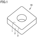
- Fig. 1 is a perspective view illustrating one embodiment of the substrate of the cutting tool.
- the substrate having such a shape is used as a substrate of an indexable cutting insert for turning, for example.
- Substrate 10 has a rake face 1, a flank face 2, and a cutting edge ridgeline portion 3 at which rake face 1 and flank face 2 cross each other. That is, rake face 1 and flank face 2 are surfaces connected to each other with cutting edge ridgeline portion 3 being interposed therebetween.
- Cutting edge ridgeline portion 3 constitutes a cutting edge tip portion of substrate 10.
- the shape of such a substrate 10 can also be regarded as the shape of the above-described cutting tool.
- a substrate 10 having a chip breaker or a substrate 10 having no chip breaker may be included.
- the shape of cutting edge ridgeline portion 3 includes any of a sharp edge (a ridge where the rake face and the flank face cross each other), a honed edge (a sharp edge processed to be rounded), a negative land (beveled), and a combination of the honed edge and the negative land.
- cutting tool 50 described above has rake face 1, flank face 2, and cutting edge ridgeline portion 3 that connects rake face 1 and flank face 2 to each other (see Fig. 6 ).
- a coating film 40 according to the present embodiment includes an ⁇ -Al 2 O 3 layer 20 provided on substrate 10 (see Fig. 6 ).
- the "coating film” has a function of improving various characteristics in the cutting tool such as chipping resistance and wear resistance by coating at least a portion (for example, a portion to be brought into contact with a workpiece during cutting) of the rake face.
- the coating film is not limited to coat a portion of the rake face, and preferably coats the entire surface of the rake face.
- the coating film may coat the entire surface of the substrate. However, a coating film that does not coat a portion of the rake face and a coating film having a partially different configuration are not deviated from the scope of the present embodiment.
- the thickness of the coating film is preferably more than or equal to 3 ⁇ m and less than or equal to 50 ⁇ m, and is more preferably more than or equal to 5 ⁇ m and less than or equal to 25 ⁇ m.
- the thickness of the coating film refers to a total of respective thicknesses of layers included in the coating film.
- Examples of the "layers included in the coating film” include an ⁇ -Al 2 O 3 layer, an intermediate layer, an underlying layer, an outermost layer, and the like, which are described below.
- the ⁇ -Al 2 O 3 layer of the present invention includes crystal grains of ⁇ -Al 2 O 3 (aluminum oxide having an ⁇ type crystal structure) (hereinafter, also simply referred to as "crystal grains"). That is, the ⁇ -Al 2 O 3 layer is a layer including polycrystal ⁇ -Al 2 O 3 .
- the ⁇ -Al 2 O 3 layer may be provided directly on the substrate or may be provided on the substrate with another layer such as the below-described intermediate layer being interposed therebetween as long as the effects exhibited by the cutting tool according to the present embodiment are not compromised.
- another layer such as an outermost layer may be provided on the ⁇ -Al 2 O 3 layer.
- the ⁇ -Al 2 O 3 layer may be the outermost layer (outermost surface layer) of the coating film.
- the area ratio of the crystal grains oriented in (001) may be more than or equal to 50% and less than or equal to 90% in the color map.
- the processed surface of the ⁇ -Al 2 O 3 layer is parallel to the surface of the substrate at the rake face.
- the ⁇ -Al 2 O 3 layer has a particular orientation ((001) orientation), whereby the cutting tool of the present embodiment can sufficiently obtain an effect of improving the strength of the coating film.
- an area ratio of crystal grains oriented in (001) in the ⁇ -Al 2 O 3 layer at a surface of the substrate other than the rake face may be more than or equal to 50% and less than or equal to 90% or may have a value falling out of the range of more than or equal to 50% and less than or equal to 90% in the cutting tool of the present embodiment.
- crystal grains of ⁇ -Al 2 O 3 oriented in (001) or the “crystal grains oriented in (001)” refer to crystal grains of ⁇ -Al 2 O 3 in each of which an inclination angle of the (001) plane (an angle formed between the normal line of a surface (facing the coating film) of the substrate and the normal line of the (001) plane) is 0 to 20° relative to the normal line of the surface of the substrate.
- an inclination angle of the (001) plane an angle formed between the normal line of a surface (facing the coating film) of the substrate and the normal line of the (001) plane
- EBSD apparatus electron backscatter diffraction apparatus
- the electron backscatter diffraction image analysis is an analysis method based on automatic analysis of a Kikuchi diffraction pattern generated by backscattered electrons.
- the "crystal grains other than the crystal grains of ⁇ -Al 2 O 3 oriented in (001)” or the “crystal grains other than the crystal grains oriented in (001)” refer to crystal grains of ⁇ -Al 2 O 3 in each of which the inclination angle of the (001) plane is more than 20° relative to the normal line of the surface of the substrate.
- an FE-SEM including an EBSD apparatus is used to capture an image of the mirror-polished, processed surface of the ⁇ -Al 2 O 3 layer parallel to the surface of the substrate at the rake face.
- an angle is calculated which is formed between the normal direction of the (001) plane of each pixel of the captured image and the normal direction of the surface of the substrate (i.e., the linear direction of the processed surface parallel to the thickness direction of the ⁇ -Al 2 O 3 layer).
- pixels in each of which the angle is 0 to 20° are selected.
- Each of the selected pixels corresponds to a crystal grain of ⁇ -Al 2 O 3 in which the inclination angle of the (001) plane is 0 to 20° relative to the surface of the substrate, i.e., corresponds to the "crystal grain of ⁇ -Al 2 O 3 oriented in (001)".
- the area ratio of the crystal grains of ⁇ -Al 2 O 3 oriented in (001) at a predetermined region (i.e., a color map) of the processed surface of the ⁇ -Al 2 O 3 layer is calculated based on the color map prepared by providing colors to the selected pixels for the purpose of classification for the processed surface of the ⁇ -Al 2 O 3 layer as crystal orientation mapping.
- a predetermined region i.e., a color map
- the calculation of the formed angle, the selection of the pixels in each of which the angle is 0 to 20°, and the calculation of the area ratio can be performed using commercially available software (trademark: "Orientation Imaging Microscopy Ver 6.2" provided by EDAX), for example.
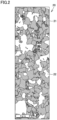
- Fig. 2 shows an exemplary color map for the above-described processed surface of ⁇ -Al 2 O 3 layer 20.
- crystal grains 21 oriented in (001) are represented by regions that are surrounded by solid lines and that are indicated by left oblique hatchings
- crystal grains 22 other than the crystal grains oriented in (001) are represented by regions that are surrounded by solid lines and that are indicated by a white color. That is, in the color map illustrated in Fig. 2 , the left oblique hatchings represent the crystal grains in each of which the angle of the normal direction of the (001) plane relative to the normal direction of the surface of ⁇ -Al 2 O 3 layer 20 is 0 to 20°.
- the white color represents the crystal grains in each of which the angle of the normal direction of the (001) plane relative to the normal direction of the surface of ⁇ -Al 2 O 3 layer 20 is more than 20°.
- the processed surface of the ⁇ -Al 2 O 3 layer includes a portion in which the area ratio of the crystal grains of ⁇ -Al 2 O 3 oriented in (001) is more than or equal to 50% and less than or equal to 90%.
- the area ratio of the crystal grains of ⁇ -Al 2 O 3 oriented in (001) is preferably more than or equal to 50% and less than or equal to 90%, and is more preferably more than or equal to 55% and less than or equal to 85%.
- an observation magnification of the FE-SEM is set to 5000x. Moreover, an observed area is set to 450 ⁇ m 2 (30 ⁇ m ⁇ 15 ⁇ m). The number of measurement fields is set to more than or equal to 3.
- the thickness of the ⁇ -Al 2 O 3 layer is more than or equal to 1 ⁇ m and less than or equal to 20 ⁇ m, and is more preferably more than or equal to 4 ⁇ m and less than or equal to 15 ⁇ m.
- the "residual stress” refers to one type of internal stress (inherent strain) in a layer.
- the residual stress is divided roughly into a compressive residual stress and a tensile residual stress.
- the compressive residual stress refers to a residual stress represented by a numerical value with a negative sign "-" (minus) (indicated by "MPa” as a unit in the present specification).
- MPa negative sign
- a “compressive residual stress of 100 MPa” is a residual stress of -100 MPa.
- a concept “large compressive residual stress” indicates that the absolute value of the above-described numerical value is large
- a concept "small compressive residual stress” indicates that the absolute value of the above-described numerical value is small.
- the tensile residual stress refers to a residual stress represented by a numerical value with a positive sign "+" (plus) (indicated by "MPa” as a unit in the present specification).
- MPa tensile residual stress
- a “tensile residual stress of 100 MPa” is a residual stress of 100 MPa.
- a concept "large tensile residual stress” indicates that the above-described numerical value is large, and a concept "small tensile residual stress” indicates that the numerical value is small.
- film residual stress A A determined based on the crystal plane interval of the (001) plane at the rake face refers to a residual stress that reflects a whole of a predetermined measurement visual field at the rake face and that is calculated based on the crystal plane interval of the (001) plane in the whole of the predetermined measurement visual field.
- Film residual stress A A is calculated by the residual stress measurement performed in accordance with the 2 ⁇ -sin 2 ⁇ method using X rays. A specific method thereof is as follows. First, for the whole of the measurement visual field, the crystal plane interval of the (001) plane is measured in accordance with the 20-sin 2 ⁇ method.
- the residual stress is measured in accordance with the 20-sin 2 ⁇ method under the following conditions.
- film residual stress B A determined based on the crystal plane interval of the (110) plane at the rake face refers to a residual stress that reflects a whole of a predetermined measurement visual field at the rake face and that is calculated based on the crystal plane interval of the (110) plane in the whole of the predetermined measurement visual field.
- Film residual stress B A is calculated by the residual stress measurement performed in accordance with the 2 ⁇ -sin 2 ⁇ method using X rays. A specific method thereof is as follows. First, for the whole of the measurement visual field, the crystal plane interval of the (110) plane is measured in accordance with the 20-sin 2 ⁇ method.
- the measurement visual field described above refers to a "measurement visual field at the surface of the ⁇ -Al 2 O 3 layer”.
- the residual stress of the whole of the measurement visual field is calculated.
- Such measurement is performed at a plurality of measurement visual fields, and the average value of respective residual stresses calculated in the measurement visual fields is regarded as "film residual stress B A ".
- the virtual plane D1 being located at a distance d 10 from a surface of the ⁇ -Al 2 O 3 layer opposite to the substrate toward the substrate side, the distance d 10 being 10% of the thickness of the ⁇ -Al 2 O 3 layer, the virtual plane D2 being located at a distance d 40 from the surface of the ⁇ -Al 2 O 3 layer opposite to the substrate toward the substrate side, the distance d 40 being 40% of the thickness of the ⁇ -Al 2 O 3 layer,
- the ⁇ -Al 2 O 3 layer has a thickness of more than or equal to 1 ⁇ m and less than or equal to 20 ⁇ m, in a residual stress measurement performed in accordance with a constant penetration depth method using X rays at a region r1 interposed between a virtual plane D1 and a virtual plane D2, the virtual plane D1 being located at a distance d 10 from a surface of the ⁇ -Al 2 O 3 layer opposite to the substrate toward the substrate side, the distance d 10 being 10% of the thickness of the ⁇ -Al 2 O 3 layer, the virtual plane D2 being located at a distance d 40 from the surface of the ⁇ -Al 2 O 3 layer opposite to the substrate toward the substrate side, the distance d 40 being 40% of the thickness of the ⁇ -Al 2 O 3 layer,
- the residual stress is measured in accordance with the constant penetration depth method under the following conditions.
- residual stress B determined based on the crystal plane interval of the (110) plane at the rake face refers to a residual stress at a predetermined depth location of the rake face, the residual stress being calculated based on the crystal plane interval of the (110) plane. Residual stress B is calculated in accordance with the constant penetration depth method using X rays.
- the constant penetration depth method is also employed to measure residual stress A d40 and residual stress B d40 at a visual field located on virtual plane D2 just below the certain measurement visual field on the virtual plane D1 within the same region as the region in which the certain measurement visual field is located.
- (3) When measured residual stresses A d10 and A d40 and residual stresses B d10 and B d40 fall within the above-described respective numerical ranges and A d10 >B d10 and A d40 > B d40 are satisfied, it is determined that "residual stress A and residual stress B fall within the respective numerical ranges at region r1 and the relational expression of A>B is satisfied".
- a stress distribution of the residual stress A has
- the stress distribution (curve a of Fig. 4 ) of residual stress A in the thickness direction of ⁇ -Al 2 O 3 layer 20 includes: a first a region P1a in which the value of the residual stress is decreased continuously from the upper surface side (the surface side or the surface side opposite to the substrate) toward the lower surface side (the substrate side); and a second a region P2a which is located at the lower surface side relative to the first a region and in which the value of the residual stress is increased continuously from the upper surface side toward the lower surface side.
- the second a region has a point at which the residual stress is changed from the compressive residual stress to the tensile residual stress.
- the first a region and the second a region are preferably continuous to each other via a minimum point P3a at which the value of the residual stress becomes minimum. This minimum point P3a is located at a location close to the upper surface relative to the lower surface.
- ⁇ -Al 2 O 3 layer 20 Since ⁇ -Al 2 O 3 layer 20 has the above-described stress distribution, a balance between the crater wear resistance and chipping resistance of ⁇ -Al 2 O 3 layer 20 becomes more excellent in intermittent cutting. This is due to the following reason: an impact applied to ⁇ -Al 2 O 3 layer 20 from the upper surface side of ⁇ -Al 2 O 3 layer 20 is absorbed sufficiently between the upper surface side and minimum point P3a, and a high crack progression resistance is exhibited at the lower surface side relative to minimum point P3a.
- a stress distribution of the residual stress B has
- the value of the residual stress is preferably more than or equal to -2000 MPa and less than or equal to 1000 MPa.
- the absolute value of the compressive residual stress is preferably less than or equal to 2000 MPa (i.e., more than or equal to -2000 MPa and less than 0 MPa)
- the absolute value of the tensile residual stress is preferably less than or equal to 1000 MPa (i.e., more than 0 MPa and less than or equal to 1000 MPa). In this case, both the chipping resistance and the crater wear resistance tend to be exhibited appropriately.
- minimum point P3b is preferably positioned to have a distance of 0.1 to 40% of the thickness of the ⁇ -Al 2 O 3 layer 20 from the surface (upper surface) opposite to the substrate.
- a damage form of ⁇ -Al 2 O 3 layer 20 becomes stable to suppress, for example, sudden chipping of the coating film, whereby variation in the life of the tool can be reduced.
- the location of minimum point P3b is preferably 0.1 to 8 ⁇ m from the surface opposite to the substrate.
- the value of the residual stress at minimum point P3b is preferably -1900 to -100 MPa, is more preferably -1800 to - 200 MPa, and is further preferably -1700 to -300 MPa.
- the average grain size of the crystal grains of ⁇ -Al 2 O 3 is preferably 0.1 ⁇ m to 3 ⁇ m, and is more preferably 0.2 ⁇ m to 2 ⁇ m.
- the average grain size of the crystal grains can be calculated using the above-described color map. Specifically, first, in the above-described color map, a region having the same color (i.e., the same plane orientation) and surrounded by different color(s) (i.e., different plane orientation(s)) is regarded as an individual region of each crystal grain. Next, a distance between two points on the outer circumference of each crystal grain is measured, and the longest distance between two points thereon is regarded as the grain size of the crystal grain.
- the coating film preferably further includes one or more intermediate layers disposed between the substrate and the ⁇ -Al 2 O 3 layer.
- Each of the intermediate layers preferably includes a compound that is composed of at least one element selected from a group consisting of a group 4 element, a group 5 element, a group 6 element in a periodic table, Al and Si, and at least one element selected from a group consisting of C, N, B, and O.
- the group 4 element in the periodic table include titanium (Ti), zirconium (Zr), hafnium (Hf) and the like.
- Examples of the group 5 element in the periodic table include vanadium (V), niobium (Nb), tantalum (Ta) and the like.
- the intermediate layer more preferably includes a Ti compound composed of a Ti element and at least one element selected from a group consisting of C, N, B, and O.
- Examples of the compound included in the intermediate layer includes TiCNO, TiAlN, TiAlSiN, TiCrSiN, TiAlCrSiN, AlCrN, AlCrO, AlCrSiN, TiZrN, TiAlMoN, TiAlNbN, TiSiN, AlCrTaN, AlTiVN, TiB 2 , TiCrHfN, CrSiWN, TiAlCN, TiSiCN, AlZrON, AlCrCN, AlHfN, CrSiBON, TiAlWN, AlCrMoCN, TiAlBN, TiAlCrSiBCNO, ZrN, ZrCN and the like.
- the thickness of the intermediate layer is preferably more than or equal to 0.1 ⁇ m and less than or equal to 3 ⁇ m, and is more preferably more than or equal to 0.5 ⁇ m and less than or equal to 1.5 ⁇ m.
- the coating film may further include other layer(s).
- the other layer(s) may have a composition different from or the same as the composition of the ⁇ -Al 2 O 3 layer or the intermediate layer.
- a compound included in the other layer(s) include TiN, TiCN, TiBN, Al 2 O 3 , and the like. It should be noted that an order of layering the other layer(s) is particularly not limited. Examples of the other layer(s) includes: an underlying layer provided between the substrate and the ⁇ -Al 2 O 3 layer; an outermost layer provided on the ⁇ -Al 2 O 3 layer; and the like.
- each of the other layer(s) is not particularly limited as long as the effects of the present embodiment are not compromised.
- the thickness of each of the other layer(s) is more than or equal to 0.1 ⁇ m and less than or equal to 20 ⁇ m.
- a method for manufacturing the cutting tool according to the present invention includes:
- the substrate having the rake face is prepared.
- a cemented carbide substrate is prepared as the substrate.
- a commercially available cemented carbide substrate may be used or a cemented carbide substrate may be produced using a general powder metallurgy method.
- WC powder, Co powder, and the like are mixed using a ball mill or the like to obtain a powder mixture.
- This powder mixture is dried and then is formed into a predetermined shape, thereby obtaining a shaped body. Further, by sintering the shaped body, a WC-Co based cemented carbide (sintered material) is obtained.
- this sintered material is subjected to a predetermined cutting edge process such as honing, thereby producing a substrate composed of the WC-Co based cemented carbide.
- a predetermined cutting edge process such as honing
- any conventionally known substrate of this type other than the above-described substrate can be prepared.
- the coating film including the ⁇ -Al 2 O 3 layer is formed on the rake face of the substrate using the chemical vapor deposition method (CVD method).
- Fig. 5 is a schematic cross sectional view showing an exemplary chemical vapor deposition apparatus (CVD apparatus) used to manufacture the coating film.
- CVD apparatus 30 includes: a plurality of substrate setting jigs 31 for holding substrates 10; and a reaction container 32 that is composed of a heat-resistant alloy steel and that covers substrate setting jigs 31.
- a temperature adjusting apparatus 33 for controlling a temperature in reaction container 32 is provided to surround reaction container 32.
- a gas inlet pipe 35 having a gas inlet 34 is provided in reaction container 32.
- Gas inlet pipe 35 is disposed to extend in the vertical direction and to be rotatable with respect to the vertical direction in an internal space of reaction container 32 in which substrate setting jigs 31 are disposed, and is provided with a plurality of jet holes 36 for jetting a gas into reaction container 32.
- each of the layers of the coating film, inclusive of the ⁇ -Al 2 O 3 layer can be formed as follows.
- each of substrates 10 is disposed on a substrate setting jig 31, and a source material gas for ⁇ -Al 2 O 3 layer 20 is introduced from gas inlet pipe 35 into reaction container 32 while controlling the temperature and pressure in reaction container 32 to fall within predetermined ranges. Accordingly, ⁇ -Al 2 O 3 layer 20 is formed on the rake face of substrate 10.
- the source material gas for the intermediate layer is not particularly limited, examples of the source material gas for the intermediate layer include: a mixed gas of TiCl 4 and N 2 ; a mixed gas of TiCl 4 , N 2 , and CH 3 CN; and a mixed gas of TiCl 4 , N 2 , CO, and CH 4 .
- the temperature in reaction container 32 during the formation of the intermediate layer is preferably controlled to fall within a range of 1000 to 1100°C, and the pressure in reaction container 32 is preferably controlled to fall within a range of 0.1 to 1013 hPa.
- HCl gas may be introduced together with the above-described source material gas. The introduction of HCl gas leads to improved uniformity of the thickness of each layer. It should be noted that it is preferable to use H 2 as a carrier gas.
- ⁇ -Al 2 O 3 layer 20 is formed on the intermediate layer.
- a source material gas a mixed gas of AlCl 3 , N 2 , CO 2 , and H 2 S is used.
- respective flow rates (L/min) of CO 2 and H 2 S are set to satisfy CO 2 /H 2 S ⁇ 2. Accordingly, the ⁇ -Al 2 O 3 layer is formed.
- the upper limit value of CO 2 /H 2 S is not particularly limited, but is preferably less than or equal to 5 in view of uniformity of the thickness of the layer.
- flow rates of CO 2 and H 2 S are preferably 0.4 to 2.0 L/min and 0.1 to 0.8 L/min, and are most preferably 1 L/min and 0.5 L/min, respectively.
- the temperature in reaction container 32 is preferably controlled to fall within a range of 1000 to 1100°C, and the pressure in reaction container 32 is preferably controlled to fall within a range of 0.1 to 100 hPa.
- HCl gas may be introduced together with the above-described source material gas, and H 2 can be used as a carrier gas. It should be noted that when introducing the gases, it is preferable to rotate gas inlet pipe 35 as with the foregoing case.
- a rate hereinafter, also referred to as "temperature decreasing rate” of 0.1 to 0.3°C/minute for a time (hereinafter, also referred to as “temperature decreasing time") of more than or equal to 30 minutes and less than 90 minutes, preferably more than or equal to 30 minutes and less than or equal to 80 minutes, at a final stage of the formation of the ⁇ -Al 2 O 3 layer.
- a tensile residual stress generated in the coating film becomes small, with the result that in the subsequent step of performing a blasting process, a tensile stress can be reduced and a compressive stress can be introduced more effectively.
- an outermost layer may be formed on ⁇ -Al 2 O 3 layer 20 as long as the effects exhibited by the cutting tool according to the present embodiment are not compromised.
- a method for forming the outermost layer is not particularly limited. Examples thereof include a method for forming the outermost layer using the CVD method or the like.
- a configuration of each layer is changed by controlling conditions of the CVD method.
- the composition of each layer is determined by the composition of the source material gas to be introduced into reaction container 32, and the thickness of each layer is controlled by an execution time (film formation time).
- an execution time film formation time.
- the ⁇ -Al 2 O 3 layer at the rake face is subjected to the blasting process.
- the "blasting process” refers to a process for changing various characteristics of the surface such as orientation and compressive stress by hitting (blasting with) a multiplicity of small spherical bodies (media) such as steel or nonferrous metal (for example, ceramic) against a surface such as the rake face at a high speed.
- the blasting process is performed onto the rake face to provide a residual stress to the ⁇ -Al 2 O 3 layer on the rake face, thus resulting in a difference between film residual stress A A and film residual stress B A .
- the blasting with the media is not particularly limited as long as film residual stress A A and film residual stress B A in the ⁇ -Al 2 O 3 layer are provided to fall within the above-described respective predetermined numerical ranges.
- the blasting with the media may be performed directly onto the ⁇ -Al 2 O 3 layer or may be performed onto another layer (for example, the outermost layer) provided on the ⁇ -Al 2 O 3 layer.
- the blasting with the media is not particularly limited as long as the blasting with the media is performed at least onto the rake face. For example, the blasting with the media may be performed onto the entire surface of the cutting tool.
- the blasting process has been performed to change, into a compressive stress, a tensile stress remaining mainly in a target layer in the coating film.
- the present inventors have first found this.
- the conventional blasting process tends to involve breakage of the target layer due to the polishing of the coating film.
- the tensile residual stress generated in the ⁇ -Al 2 O 3 layer in the second step is smaller than that in the ⁇ -Al 2 O 3 layer formed in accordance with the conventional manufacturing method. Accordingly, breakage of the ⁇ -Al 2 O 3 layer does not take place and a stress is likely to be introduced into the ⁇ -Al 2 O 3 layer, with the result that film residual stress A A and film residual stress B A can become tensile residual stress and compressive residual stress falling within the predetermined numerical ranges, respectively.
- film residual stress A A and film residual stress B A become the tensile residual stress and compressive residual stress falling within the predetermined numerical ranges respectively by performing the blasting process onto the ⁇ -Al 2 O 3 layer
- the present inventors consider as follows. It is considered that the crystal grains oriented in (001) have a resistance against deformation due to external force because the crystal grains oriented in the same crystal orientation support one another. On the other hand, it is considered that the crystal grains other than the crystal grains oriented in (001) have a reduced resistance against the deformation due to external force because the crystal orientations thereof are not aligned.
- the average grain size of the media is preferably 1 to 300 ⁇ m, and is more preferably 5 to 200 ⁇ m, for example.
- a commercially available product may be used.
- examples thereof include ceramic abrasive grains each having a grain size of 90 to 125 ⁇ m (average grain size of 100 ⁇ m) (provided by NICCHU; trademark: WAF120).
- a distance (hereinafter, also referred to as "blasting distance") between a blasting unit for blasting with the media and the surface such as the rake face is preferably 80 mm to 120 mm, and is more preferably 80 mm to 100 mm.
- a pressure (hereinafter, also referred to as “blasting pressure”) to be applied to the media upon blasting is preferably 0.02 MPa to 0.5 MPa, and is more preferably 0.05 MPa to 0.3 MPa.
- a process time for the blasting is preferably 5 seconds to 60 seconds, and is more preferably 10 seconds to 30 seconds.
- the conditions of the blasting process can be appropriately adjusted in accordance with the configuration of the coating film.
- an additional step may be performed appropriately in addition to the steps described above, as long as the effects of the blasting process are not compromised.
- cemented carbide cutting inserts shape: CNMG120408N-UX; provided by Sumitomo Electric Industries HardMetal; JIS B4120 (2013)
- a CVD apparatus was used to form an intermediate layer and an ⁇ -Al 2 O 3 layer in this order on each of the prepared substrates, thereby forming a coating film on a surface of the substrate including a rake face.
- the ⁇ -Al 2 O 3 layer was directly formed on the substrate without forming the intermediate layer (sample numbers 8 and 13). Conditions for forming each layer are described below.
- a temperature was decreased at a temperature decreasing rate shown in Table 2 for a temperature decreasing time shown in Table 2.
- a cell with "-" in Table 2 means that a corresponding process was not performed. It should be noted that a value in parenthesis following each gas composition indicates a flow rate (L/min) of each gas.
- the thickness of the ⁇ -Al 2 O 3 layer and the thickness and composition of the intermediate layer are shown in Table 1.
- Mirror-polishing was performed to produce a processed surface of the ⁇ -Al 2 O 3 layer so as to be parallel to the surface of the substrate at the rake face of the cutting tool having the coating film provided thereon.
- the produced processed surface was observed at a magnification of 5000x using an FE-SEM including an EBSD, thereby preparing the above-described color map for the processed surface with 30 ⁇ m ⁇ 15 ⁇ m.
- the number of color maps prepared on this occasion was 3.
- Table 3 shows residual stresses A (A d10 , A d40 ) and B (B d10 , B d40 ) at representative depth locations.
- first a region P1a and second a region P2a first b region P1b and second b region P2b
- minimum point P3b was determined to exist therein (Table 3).
- each of the cutting tools of sample numbers 1 to 8 (Examples) attained such an excellent result that the number of times of making contact with the workpiece until the chipping and detachment occurred in the intermittent process was more than or equal to 5000.
- the number of times of making contact in the intermittent process was less than 5000. From the above results, it was found that each of the cutting tools of the Examples (sample numbers 1 to 8) was excellent in chipping resistance.
- each of the cutting tools of sample numbers 1 to 8 (Examples) attained such an excellent result that the cutting time in the continuous process was more than or equal to 20 minutes.
- the cutting time in the continuous process was less than 20 minutes. From the above results, it was found that each of the cutting tools of the Examples (sample numbers 1 to 8) was excellent in crater wear resistance.
- a method for manufacturing the cutting tool comprising:
Landscapes
- Chemical & Material Sciences (AREA)
- Engineering & Computer Science (AREA)
- Mechanical Engineering (AREA)
- Metallurgy (AREA)
- Organic Chemistry (AREA)
- Chemical Kinetics & Catalysis (AREA)
- Materials Engineering (AREA)
- Inorganic Chemistry (AREA)
- General Chemical & Material Sciences (AREA)
- Ceramic Engineering (AREA)
- Cutting Tools, Boring Holders, And Turrets (AREA)
- Chemical Vapour Deposition (AREA)
- Drilling Tools (AREA)
Claims (4)
- Outil de découpe comprenant :un substrat comprenant une face aplanie ; etun film de revêtement qui recouvre la surface aplanie, dans lequelle film de revêtement comprend une couche de α-Al2O3 disposée sur le substrat,la couche de α-Al2O3 comprend des grains cristallins de α-Al2O3,un rapport de surface des grains cristallins orientés en (001) parmi les grains cristallins est supérieur ou égal à 50 % et inférieur ou égal à 90 % dans la couche de α-Al2O3 au niveau de la surface aplanie, dans lequel le rapport de surface est mesuré par le procédé décrit dans la description,caractérisé en ce quelors d'une mesure de contrainte résiduelle effectuée selon un procédé 2θ-sin2ψ qui utilise des rayons X, tel que décrit dans la description,une contrainte résiduelle de film AA déterminée sur la base d'un intervalle de plan cristallin d'un plan (001) de la couche de α-Al2O3 au niveau de la face aplanie est supérieure à 0 MPa et inférieure ou égale à 2000 MPa, etune contrainte résiduelle de film BA déterminée sur la base d'un intervalle de plan cristallin d'un plan (110) de la couche de α-Al2O3 au niveau de la face aplanie est supérieure ou égale à -1000 MPa et inférieure à 0 MPa, et dans lequella couche de α-Al2O3 présente une épaisseur supérieure ou égale à 1 µm et inférieure ou égale à 20 µm, etlors d'une mesure de contrainte résiduelle effectuée selon un procédé à profondeur de pénétration constante qui utilise des rayons X au niveau d'une zone r1 interposée entre un plan virtuel D1 et un plan virtuel D2, le plan virtuel D1 étant situé à une distance d10 par rapport à une surface de la couche de α-Al2O3 opposée au substrat vers le côté substrat, la distance d10 étant égale à 10 % de l'épaisseur de la couche de α-Al2O3, le plan virtuel D2 étant situé à une distance d40 de la surface de la couche de α-Al2O3 opposée au substrat vers le côté substrat, la distance d40 étant égale à 40 % de l'épaisseur de la couche de α-Al2O3, comme cela est décrit dans la description,une contrainte résiduelle A déterminée sur la base de l'intervalle de plan cristallin du plan (001) de la couche de α-Al2O3 au niveau de la face aplanie est supérieure ou égale à -200 MPa et inférieure ou égale à 2000 MPa, etune contrainte résiduelle B déterminée sur la base de l'intervalle de plan cristallin du plan (110) de la couche de α-Al2O3 au niveau de la face aplanie est supérieure ou égale à -1500 MPa et inférieure ou égale à 700 MPa, etune expression relationnelle de A>B est satisfaite.
- Outil de découpe selon la revendication 1, dans lequelune répartition de contrainte de la contrainte résiduelle A présente une première zone a dans laquelle la contrainte résiduelle A est réduite en continu par rapport à la surface de la couche de α-Al2O3 opposée au substrat vers le côté substrat, etune deuxième zone a qui se trouve côté substrat par rapport à la première zone a et dans laquelle la contrainte résiduelle A est augmentée en continu par rapport à la surface opposée au substrat vers le côté substrat, etla première zone a et la deuxième zone a sont continues l'une par rapport à l'autre via un point minimum de la contrainte résiduelle A.
- Outil de découpe selon la revendication 1 ou la revendication 2, dans lequelune répartition de contrainte de la contrainte résiduelle B présente une première zone b dans laquelle la contrainte résiduelle B est réduite en continu par rapport à la surface de la couche de α-Al2O3 opposée au substrat vers le côté substrat, etune deuxième zone b qui se trouve côté substrat par rapport à la première zone b et dans laquelle la contrainte résiduelle B est augmentée en continu par rapport à la surface opposée au substrat vers le côté substrat, etla première zone b et la deuxième zone b sont continues l'une par rapport à l'autre via un point minimum de la contrainte résiduelle B.
- Outil de découpe selon l'une quelconque de la revendication 1 à la revendication 3, dans lequelle film de revêtement comprend en outre une ou plusieurs couche(s) intermédiaire(s) disposée(s) entre le substrat et la couche de α-Al2O3, etchacune des couches intermédiaires comprend un composé qui est composé d'au moins un élément choisi parmi un groupe consistant en un élément de groupe 4, un élément de groupe 5, un élément de groupe 6 dans un tableau périodique, Al et Si, et au moins un élément choisi parmi un groupe consistant en C, N, B et O.
Applications Claiming Priority (2)
| Application Number | Priority Date | Filing Date | Title |
|---|---|---|---|
| JP2018194134 | 2018-10-15 | ||
| PCT/JP2019/026821 WO2020079894A1 (fr) | 2018-10-15 | 2019-07-05 | Outil de coupe |
Publications (3)
| Publication Number | Publication Date |
|---|---|
| EP3868502A1 EP3868502A1 (fr) | 2021-08-25 |
| EP3868502A4 EP3868502A4 (fr) | 2022-04-27 |
| EP3868502B1 true EP3868502B1 (fr) | 2025-04-16 |
Family
ID=70284510
Family Applications (1)
| Application Number | Title | Priority Date | Filing Date |
|---|---|---|---|
| EP19873707.4A Active EP3868502B1 (fr) | 2018-10-15 | 2019-07-05 | Outil de coupe |
Country Status (5)
| Country | Link |
|---|---|
| US (1) | US11167355B2 (fr) |
| EP (1) | EP3868502B1 (fr) |
| KR (1) | KR102495052B1 (fr) |
| CN (1) | CN112839761B (fr) |
| WO (1) | WO2020079894A1 (fr) |
Families Citing this family (1)
| Publication number | Priority date | Publication date | Assignee | Title |
|---|---|---|---|---|
| CN119654208A (zh) * | 2022-08-31 | 2025-03-18 | 京瓷株式会社 | 涂层刀具以及切削刀具 |
Family Cites Families (24)
| Publication number | Priority date | Publication date | Assignee | Title |
|---|---|---|---|---|
| JP2004284003A (ja) | 2003-02-28 | 2004-10-14 | Mitsubishi Materials Corp | 硬質被覆層がすぐれた耐チッピング性を発揮する表面被覆サーメット製切削工具 |
| SE531929C2 (sv) | 2007-07-13 | 2009-09-08 | Seco Tools Ab | Belagt hårdmetallskär för svarvning av stål eller rostfritt stål |
| JP5383259B2 (ja) | 2009-03-10 | 2014-01-08 | 京セラ株式会社 | 切削工具 |
| EP2287359B1 (fr) * | 2009-07-03 | 2012-05-23 | Sandvik Intellectual Property AB | Plaquette de coupe enrobée |
| JP5321975B2 (ja) * | 2009-09-24 | 2013-10-23 | 住友電工ハードメタル株式会社 | 表面被覆切削工具 |
| US8715838B2 (en) | 2010-11-10 | 2014-05-06 | Sumitomo Electric Hardmetal Corp. | Surface-coated cutting tool |
| JP5760640B2 (ja) * | 2011-04-21 | 2015-08-12 | 住友電気工業株式会社 | 被覆切削工具 |
| DE102011053705A1 (de) * | 2011-09-16 | 2013-03-21 | Walter Ag | Schneideinsatz und Verfahren zu dessen Herstellung |
| JP5757232B2 (ja) * | 2011-12-26 | 2015-07-29 | 三菱マテリアル株式会社 | 硬質被覆層がすぐれた耐チッピング性と耐摩耗性を発揮する表面被覆切削工具 |
| BR112016017108B1 (pt) * | 2014-01-27 | 2020-12-15 | Tungaloy Corporation | Ferramenta de corte revestida |
| JP6421934B2 (ja) * | 2014-02-26 | 2018-11-14 | 三菱マテリアル株式会社 | 耐異常損傷性と耐摩耗性に優れた表面被覆切削工具 |
| JP2016165789A (ja) * | 2015-03-10 | 2016-09-15 | 三菱マテリアル株式会社 | 硬質被覆層がすぐれた耐チッピング性と耐摩耗性を発揮する表面被覆切削工具 |
| JP6738556B2 (ja) * | 2015-06-26 | 2020-08-12 | 三菱マテリアル株式会社 | 表面被覆切削工具 |
| US9878373B2 (en) * | 2015-07-13 | 2018-01-30 | Sumitomo Electric Hardmetal Corp. | Surface-coated cutting tool |
| JP7160677B2 (ja) * | 2015-07-27 | 2022-10-25 | ヴァルター アーゲー | TiAlNコーティングを有する工具とその工具の製造方法 |
| KR102107878B1 (ko) | 2015-08-28 | 2020-05-07 | 스미또모 덴꼬오 하드메탈 가부시끼가이샤 | 표면 피복 절삭 공구 |
| KR102027028B1 (ko) * | 2015-08-28 | 2019-09-30 | 스미또모 덴꼬오 하드메탈 가부시끼가이샤 | 표면 피복 절삭 공구 |
| US9844816B2 (en) | 2015-10-09 | 2017-12-19 | Sumitomo Electric Hardmetal Corp. | Surface-coated cutting tool |
| US9849517B2 (en) * | 2015-10-09 | 2017-12-26 | Sumitomo Electric Hardmetal Corp. | Surface-coated cutting tool and method of manufacturing the same |
| US9863064B2 (en) * | 2015-10-09 | 2018-01-09 | Sumitomo Electric Hardmetal Corp. | Surface-coated cutting tool |
| JP6507456B2 (ja) * | 2016-01-08 | 2019-05-08 | 住友電工ハードメタル株式会社 | 表面被覆切削工具の製造方法 |
| JP6507457B2 (ja) * | 2016-01-08 | 2019-05-08 | 住友電工ハードメタル株式会社 | 表面被覆切削工具の製造方法 |
| JP6604553B2 (ja) | 2016-03-30 | 2019-11-13 | 三菱マテリアル株式会社 | 表面被覆切削工具 |
| JP6865635B2 (ja) | 2017-05-19 | 2021-04-28 | 株式会社ブリヂストン | 液圧式アクチュエータ |
-
2019
- 2019-07-05 EP EP19873707.4A patent/EP3868502B1/fr active Active
- 2019-07-05 US US16/637,038 patent/US11167355B2/en active Active
- 2019-07-05 CN CN201980067838.3A patent/CN112839761B/zh active Active
- 2019-07-05 KR KR1020217010761A patent/KR102495052B1/ko active Active
- 2019-07-05 WO PCT/JP2019/026821 patent/WO2020079894A1/fr not_active Ceased
Also Published As
| Publication number | Publication date |
|---|---|
| EP3868502A1 (fr) | 2021-08-25 |
| US20210008633A1 (en) | 2021-01-14 |
| EP3868502A4 (fr) | 2022-04-27 |
| WO2020079894A1 (fr) | 2020-04-23 |
| US11167355B2 (en) | 2021-11-09 |
| CN112839761A (zh) | 2021-05-25 |
| KR102495052B1 (ko) | 2023-02-06 |
| CN112839761B (zh) | 2023-08-22 |
| KR20210045498A (ko) | 2021-04-26 |
Similar Documents
| Publication | Publication Date | Title |
|---|---|---|
| EP3444052B1 (fr) | Outil de coupe revêtu en surface et procédé de fabrication pour ce dernier | |
| EP3441167B1 (fr) | Outil de coupe à revêtement de surface et son procédé de production | |
| EP3444053B1 (fr) | Outil de coupe revêtu en surface et procédé de fabrication pour ce dernier | |
| EP2594352B1 (fr) | Outil de découpage de revêtement de surface | |
| EP1722009A1 (fr) | Revetement mince resistant a l'usure | |
| EP3412386B1 (fr) | Outil de coupe revêtu en surface et procédé de fabrication pour ce dernier | |
| EP4144466B1 (fr) | Outil de coupe | |
| EP3415255B1 (fr) | Outil de coupe revêtu en surface et procédé pour sa production | |
| EP3851230B1 (fr) | Outil de coupe | |
| WO2022244242A1 (fr) | Outil de coupe | |
| EP4147808B1 (fr) | Outil de coupe | |
| EP3871814B1 (fr) | Outil de coupe | |
| EP3868502B1 (fr) | Outil de coupe | |
| EP3868501B1 (fr) | Outil de coupe | |
| JP7486045B2 (ja) | 表面被覆切削工具 | |
| EP3511097A1 (fr) | Outil de coupe, et procédé de fabrication de celui-ci | |
| US20220193787A1 (en) | Cutting tool | |
| EP3871815B1 (fr) | Méthode de fabrication d'un outil de coupe | |
| US20220168819A1 (en) | Cutting tool | |
| JP6641660B1 (ja) | 切削工具 | |
| JP2021137955A (ja) | 表面被覆切削工具 |
Legal Events
| Date | Code | Title | Description |
|---|---|---|---|
| STAA | Information on the status of an ep patent application or granted ep patent |
Free format text: STATUS: THE INTERNATIONAL PUBLICATION HAS BEEN MADE |
|
| PUAI | Public reference made under article 153(3) epc to a published international application that has entered the european phase |
Free format text: ORIGINAL CODE: 0009012 |
|
| STAA | Information on the status of an ep patent application or granted ep patent |
Free format text: STATUS: REQUEST FOR EXAMINATION WAS MADE |
|
| 17P | Request for examination filed |
Effective date: 20210406 |
|
| AK | Designated contracting states |
Kind code of ref document: A1 Designated state(s): AL AT BE BG CH CY CZ DE DK EE ES FI FR GB GR HR HU IE IS IT LI LT LU LV MC MK MT NL NO PL PT RO RS SE SI SK SM TR |
|
| DAV | Request for validation of the european patent (deleted) | ||
| DAX | Request for extension of the european patent (deleted) | ||
| A4 | Supplementary search report drawn up and despatched |
Effective date: 20220328 |
|
| RIC1 | Information provided on ipc code assigned before grant |
Ipc: C23C 16/36 20060101ALI20220322BHEP Ipc: C23C 16/455 20060101ALI20220322BHEP Ipc: C23C 16/02 20060101ALI20220322BHEP Ipc: C23C 16/56 20060101ALI20220322BHEP Ipc: C23C 30/00 20060101ALI20220322BHEP Ipc: C23C 28/04 20060101ALI20220322BHEP Ipc: C23C 16/40 20060101ALI20220322BHEP Ipc: C23C 14/08 20060101ALI20220322BHEP Ipc: B23C 5/16 20060101ALI20220322BHEP Ipc: B23B 51/00 20060101ALI20220322BHEP Ipc: B23B 27/14 20060101AFI20220322BHEP |
|
| REG | Reference to a national code |
Ref legal event code: R079 Free format text: PREVIOUS MAIN CLASS: B23B0027140000 Ipc: C23C0016400000 Ref country code: DE Ref document number: 602019068836 Country of ref document: DE |
|
| GRAP | Despatch of communication of intention to grant a patent |
Free format text: ORIGINAL CODE: EPIDOSNIGR1 |
|
| STAA | Information on the status of an ep patent application or granted ep patent |
Free format text: STATUS: GRANT OF PATENT IS INTENDED |
|
| RIC1 | Information provided on ipc code assigned before grant |
Ipc: C23C 16/36 20060101ALI20241113BHEP Ipc: C23C 16/455 20060101ALI20241113BHEP Ipc: C23C 16/02 20060101ALI20241113BHEP Ipc: C23C 16/56 20060101ALI20241113BHEP Ipc: C23C 30/00 20060101ALI20241113BHEP Ipc: C23C 28/04 20060101ALI20241113BHEP Ipc: C23C 16/40 20060101AFI20241113BHEP |
|
| INTG | Intention to grant announced |
Effective date: 20241205 |
|
| GRAS | Grant fee paid |
Free format text: ORIGINAL CODE: EPIDOSNIGR3 |
|
| GRAA | (expected) grant |
Free format text: ORIGINAL CODE: 0009210 |
|
| STAA | Information on the status of an ep patent application or granted ep patent |
Free format text: STATUS: THE PATENT HAS BEEN GRANTED |
|
| P01 | Opt-out of the competence of the unified patent court (upc) registered |
Free format text: CASE NUMBER: APP_6986/2025 Effective date: 20250211 |
|
| AK | Designated contracting states |
Kind code of ref document: B1 Designated state(s): AL AT BE BG CH CY CZ DE DK EE ES FI FR GB GR HR HU IE IS IT LI LT LU LV MC MK MT NL NO PL PT RO RS SE SI SK SM TR |
|
| REG | Reference to a national code |
Ref country code: GB Ref legal event code: FG4D |
|
| REG | Reference to a national code |
Ref country code: CH Ref legal event code: EP |
|
| REG | Reference to a national code |
Ref country code: IE Ref legal event code: FG4D |
|
| REG | Reference to a national code |
Ref country code: DE Ref legal event code: R096 Ref document number: 602019068836 Country of ref document: DE |
|
| REG | Reference to a national code |
Ref country code: SE Ref legal event code: TRGR |
|
| PGFP | Annual fee paid to national office [announced via postgrant information from national office to epo] |
Ref country code: SE Payment date: 20250610 Year of fee payment: 7 |
|
| REG | Reference to a national code |
Ref country code: NL Ref legal event code: MP Effective date: 20250416 |
|
| PG25 | Lapsed in a contracting state [announced via postgrant information from national office to epo] |
Ref country code: NL Free format text: LAPSE BECAUSE OF FAILURE TO SUBMIT A TRANSLATION OF THE DESCRIPTION OR TO PAY THE FEE WITHIN THE PRESCRIBED TIME-LIMIT Effective date: 20250416 |
|
| REG | Reference to a national code |
Ref country code: AT Ref legal event code: MK05 Ref document number: 1785711 Country of ref document: AT Kind code of ref document: T Effective date: 20250416 |
|
| PG25 | Lapsed in a contracting state [announced via postgrant information from national office to epo] |
Ref country code: PT Free format text: LAPSE BECAUSE OF FAILURE TO SUBMIT A TRANSLATION OF THE DESCRIPTION OR TO PAY THE FEE WITHIN THE PRESCRIBED TIME-LIMIT Effective date: 20250818 Ref country code: ES Free format text: LAPSE BECAUSE OF FAILURE TO SUBMIT A TRANSLATION OF THE DESCRIPTION OR TO PAY THE FEE WITHIN THE PRESCRIBED TIME-LIMIT Effective date: 20250416 Ref country code: FI Free format text: LAPSE BECAUSE OF FAILURE TO SUBMIT A TRANSLATION OF THE DESCRIPTION OR TO PAY THE FEE WITHIN THE PRESCRIBED TIME-LIMIT Effective date: 20250416 |
|
| PGFP | Annual fee paid to national office [announced via postgrant information from national office to epo] |
Ref country code: DE Payment date: 20250611 Year of fee payment: 7 |
|
| REG | Reference to a national code |
Ref country code: LT Ref legal event code: MG9D |
|
| PG25 | Lapsed in a contracting state [announced via postgrant information from national office to epo] |
Ref country code: NO Free format text: LAPSE BECAUSE OF FAILURE TO SUBMIT A TRANSLATION OF THE DESCRIPTION OR TO PAY THE FEE WITHIN THE PRESCRIBED TIME-LIMIT Effective date: 20250716 Ref country code: GR Free format text: LAPSE BECAUSE OF FAILURE TO SUBMIT A TRANSLATION OF THE DESCRIPTION OR TO PAY THE FEE WITHIN THE PRESCRIBED TIME-LIMIT Effective date: 20250717 |
|
| PG25 | Lapsed in a contracting state [announced via postgrant information from national office to epo] |
Ref country code: PL Free format text: LAPSE BECAUSE OF FAILURE TO SUBMIT A TRANSLATION OF THE DESCRIPTION OR TO PAY THE FEE WITHIN THE PRESCRIBED TIME-LIMIT Effective date: 20250416 |
|
| PG25 | Lapsed in a contracting state [announced via postgrant information from national office to epo] |
Ref country code: BG Free format text: LAPSE BECAUSE OF FAILURE TO SUBMIT A TRANSLATION OF THE DESCRIPTION OR TO PAY THE FEE WITHIN THE PRESCRIBED TIME-LIMIT Effective date: 20250416 |
|
| PG25 | Lapsed in a contracting state [announced via postgrant information from national office to epo] |
Ref country code: HR Free format text: LAPSE BECAUSE OF FAILURE TO SUBMIT A TRANSLATION OF THE DESCRIPTION OR TO PAY THE FEE WITHIN THE PRESCRIBED TIME-LIMIT Effective date: 20250416 |
|
| PG25 | Lapsed in a contracting state [announced via postgrant information from national office to epo] |
Ref country code: AT Free format text: LAPSE BECAUSE OF FAILURE TO SUBMIT A TRANSLATION OF THE DESCRIPTION OR TO PAY THE FEE WITHIN THE PRESCRIBED TIME-LIMIT Effective date: 20250416 |
|
| PG25 | Lapsed in a contracting state [announced via postgrant information from national office to epo] |
Ref country code: RS Free format text: LAPSE BECAUSE OF FAILURE TO SUBMIT A TRANSLATION OF THE DESCRIPTION OR TO PAY THE FEE WITHIN THE PRESCRIBED TIME-LIMIT Effective date: 20250716 |
|
| PG25 | Lapsed in a contracting state [announced via postgrant information from national office to epo] |
Ref country code: IS Free format text: LAPSE BECAUSE OF FAILURE TO SUBMIT A TRANSLATION OF THE DESCRIPTION OR TO PAY THE FEE WITHIN THE PRESCRIBED TIME-LIMIT Effective date: 20250816 |
|
| PG25 | Lapsed in a contracting state [announced via postgrant information from national office to epo] |
Ref country code: LV Free format text: LAPSE BECAUSE OF FAILURE TO SUBMIT A TRANSLATION OF THE DESCRIPTION OR TO PAY THE FEE WITHIN THE PRESCRIBED TIME-LIMIT Effective date: 20250416 |
|
| PG25 | Lapsed in a contracting state [announced via postgrant information from national office to epo] |
Ref country code: SM Free format text: LAPSE BECAUSE OF FAILURE TO SUBMIT A TRANSLATION OF THE DESCRIPTION OR TO PAY THE FEE WITHIN THE PRESCRIBED TIME-LIMIT Effective date: 20250416 Ref country code: DK Free format text: LAPSE BECAUSE OF FAILURE TO SUBMIT A TRANSLATION OF THE DESCRIPTION OR TO PAY THE FEE WITHIN THE PRESCRIBED TIME-LIMIT Effective date: 20250416 |
|
| REG | Reference to a national code |
Ref country code: DE Ref legal event code: R097 Ref document number: 602019068836 Country of ref document: DE |
|
| PG25 | Lapsed in a contracting state [announced via postgrant information from national office to epo] |
Ref country code: CZ Free format text: LAPSE BECAUSE OF FAILURE TO SUBMIT A TRANSLATION OF THE DESCRIPTION OR TO PAY THE FEE WITHIN THE PRESCRIBED TIME-LIMIT Effective date: 20250416 |
|
| PG25 | Lapsed in a contracting state [announced via postgrant information from national office to epo] |
Ref country code: EE Free format text: LAPSE BECAUSE OF FAILURE TO SUBMIT A TRANSLATION OF THE DESCRIPTION OR TO PAY THE FEE WITHIN THE PRESCRIBED TIME-LIMIT Effective date: 20250416 |
|
| PG25 | Lapsed in a contracting state [announced via postgrant information from national office to epo] |
Ref country code: RO Free format text: LAPSE BECAUSE OF FAILURE TO SUBMIT A TRANSLATION OF THE DESCRIPTION OR TO PAY THE FEE WITHIN THE PRESCRIBED TIME-LIMIT Effective date: 20250416 Ref country code: SK Free format text: LAPSE BECAUSE OF FAILURE TO SUBMIT A TRANSLATION OF THE DESCRIPTION OR TO PAY THE FEE WITHIN THE PRESCRIBED TIME-LIMIT Effective date: 20250416 |
|
| PG25 | Lapsed in a contracting state [announced via postgrant information from national office to epo] |
Ref country code: IT Free format text: LAPSE BECAUSE OF FAILURE TO SUBMIT A TRANSLATION OF THE DESCRIPTION OR TO PAY THE FEE WITHIN THE PRESCRIBED TIME-LIMIT Effective date: 20250416 |
|
| PLBE | No opposition filed within time limit |
Free format text: ORIGINAL CODE: 0009261 |
|
| STAA | Information on the status of an ep patent application or granted ep patent |
Free format text: STATUS: NO OPPOSITION FILED WITHIN TIME LIMIT |
|
| REG | Reference to a national code |
Ref country code: CH Ref legal event code: H13 Free format text: ST27 STATUS EVENT CODE: U-0-0-H10-H13 (AS PROVIDED BY THE NATIONAL OFFICE) Effective date: 20260224 |
|
| REG | Reference to a national code |
Ref country code: CH Ref legal event code: L10 Free format text: ST27 STATUS EVENT CODE: U-0-0-L10-L00 (AS PROVIDED BY THE NATIONAL OFFICE) Effective date: 20260225 |
|
| PG25 | Lapsed in a contracting state [announced via postgrant information from national office to epo] |
Ref country code: LU Free format text: LAPSE BECAUSE OF NON-PAYMENT OF DUE FEES Effective date: 20250705 |
|
| 26N | No opposition filed |
Effective date: 20260119 |
|
| GBPC | Gb: european patent ceased through non-payment of renewal fee |
Effective date: 20250716 |
|
| REG | Reference to a national code |
Ref country code: BE Ref legal event code: MM Effective date: 20250731 |
|
| PG25 | Lapsed in a contracting state [announced via postgrant information from national office to epo] |
Ref country code: GB Free format text: LAPSE BECAUSE OF NON-PAYMENT OF DUE FEES Effective date: 20250716 |
|
| PG25 | Lapsed in a contracting state [announced via postgrant information from national office to epo] |
Ref country code: BE Free format text: LAPSE BECAUSE OF NON-PAYMENT OF DUE FEES Effective date: 20250731 |
|
| PG25 | Lapsed in a contracting state [announced via postgrant information from national office to epo] |
Ref country code: FR Free format text: LAPSE BECAUSE OF NON-PAYMENT OF DUE FEES Effective date: 20250731 |