EP3869794A1 - Dispositif d'imagerie et dispositif d'imagerie à semi-conducteurs - Google Patents
Dispositif d'imagerie et dispositif d'imagerie à semi-conducteurs Download PDFInfo
- Publication number
- EP3869794A1 EP3869794A1 EP19873204.2A EP19873204A EP3869794A1 EP 3869794 A1 EP3869794 A1 EP 3869794A1 EP 19873204 A EP19873204 A EP 19873204A EP 3869794 A1 EP3869794 A1 EP 3869794A1
- Authority
- EP
- European Patent Office
- Prior art keywords
- light
- imaging device
- diffuser
- image sensor
- light receiver
- Prior art date
- Legal status (The legal status is an assumption and is not a legal conclusion. Google has not performed a legal analysis and makes no representation as to the accuracy of the status listed.)
- Withdrawn
Links
Images


Classifications
-
- H—ELECTRICITY
- H10—SEMICONDUCTOR DEVICES; ELECTRIC SOLID-STATE DEVICES NOT OTHERWISE PROVIDED FOR
- H10F—INORGANIC SEMICONDUCTOR DEVICES SENSITIVE TO INFRARED RADIATION, LIGHT, ELECTROMAGNETIC RADIATION OF SHORTER WAVELENGTH OR CORPUSCULAR RADIATION
- H10F39/00—Integrated devices, or assemblies of multiple devices, comprising at least one element covered by group H10F30/00, e.g. radiation detectors comprising photodiode arrays
- H10F39/80—Constructional details of image sensors
- H10F39/804—Containers or encapsulations
-
- G—PHYSICS
- G01—MEASURING; TESTING
- G01J—MEASUREMENT OF INTENSITY, VELOCITY, SPECTRAL CONTENT, POLARISATION, PHASE OR PULSE CHARACTERISTICS OF INFRARED, VISIBLE OR ULTRAVIOLET LIGHT; COLORIMETRY; RADIATION PYROMETRY
- G01J5/00—Radiation pyrometry, e.g. infrared or optical thermometry
- G01J5/02—Constructional details
- G01J5/08—Optical arrangements
- G01J5/0801—Means for wavelength selection or discrimination
- G01J5/0802—Optical filters
-
- G—PHYSICS
- G01—MEASURING; TESTING
- G01J—MEASUREMENT OF INTENSITY, VELOCITY, SPECTRAL CONTENT, POLARISATION, PHASE OR PULSE CHARACTERISTICS OF INFRARED, VISIBLE OR ULTRAVIOLET LIGHT; COLORIMETRY; RADIATION PYROMETRY
- G01J1/00—Photometry, e.g. photographic exposure meter
- G01J1/02—Details
- G01J1/0214—Constructional arrangements for removing stray light
-
- G—PHYSICS
- G01—MEASURING; TESTING
- G01J—MEASUREMENT OF INTENSITY, VELOCITY, SPECTRAL CONTENT, POLARISATION, PHASE OR PULSE CHARACTERISTICS OF INFRARED, VISIBLE OR ULTRAVIOLET LIGHT; COLORIMETRY; RADIATION PYROMETRY
- G01J1/00—Photometry, e.g. photographic exposure meter
- G01J1/02—Details
- G01J1/04—Optical or mechanical part supplementary adjustable parts
- G01J1/0407—Optical elements not provided otherwise, e.g. manifolds, windows, holograms, gratings
- G01J1/0474—Diffusers
-
- G—PHYSICS
- G01—MEASURING; TESTING
- G01J—MEASUREMENT OF INTENSITY, VELOCITY, SPECTRAL CONTENT, POLARISATION, PHASE OR PULSE CHARACTERISTICS OF INFRARED, VISIBLE OR ULTRAVIOLET LIGHT; COLORIMETRY; RADIATION PYROMETRY
- G01J5/00—Radiation pyrometry, e.g. infrared or optical thermometry
- G01J5/02—Constructional details
- G01J5/06—Arrangements for eliminating effects of disturbing radiation; Arrangements for compensating changes in sensitivity
-
- G—PHYSICS
- G01—MEASURING; TESTING
- G01J—MEASUREMENT OF INTENSITY, VELOCITY, SPECTRAL CONTENT, POLARISATION, PHASE OR PULSE CHARACTERISTICS OF INFRARED, VISIBLE OR ULTRAVIOLET LIGHT; COLORIMETRY; RADIATION PYROMETRY
- G01J5/00—Radiation pyrometry, e.g. infrared or optical thermometry
- G01J5/02—Constructional details
- G01J5/08—Optical arrangements
- G01J5/0878—Diffusers
-
- G—PHYSICS
- G02—OPTICS
- G02B—OPTICAL ELEMENTS, SYSTEMS OR APPARATUS
- G02B27/00—Optical systems or apparatus not provided for by any of the groups G02B1/00 - G02B26/00, G02B30/00
- G02B27/0018—Optical systems or apparatus not provided for by any of the groups G02B1/00 - G02B26/00, G02B30/00 with means for preventing ghost images
-
- G—PHYSICS
- G02—OPTICS
- G02B—OPTICAL ELEMENTS, SYSTEMS OR APPARATUS
- G02B5/00—Optical elements other than lenses
- G02B5/02—Diffusing elements; Afocal elements
- G02B5/0273—Diffusing elements; Afocal elements characterized by the use
- G02B5/0278—Diffusing elements; Afocal elements characterized by the use used in transmission
-
- H—ELECTRICITY
- H04—ELECTRIC COMMUNICATION TECHNIQUE
- H04N—PICTORIAL COMMUNICATION, e.g. TELEVISION
- H04N23/00—Cameras or camera modules comprising electronic image sensors; Control thereof
- H04N23/20—Cameras or camera modules comprising electronic image sensors; Control thereof for generating image signals from infrared radiation only
- H04N23/23—Cameras or camera modules comprising electronic image sensors; Control thereof for generating image signals from infrared radiation only from thermal infrared radiation
-
- H—ELECTRICITY
- H10—SEMICONDUCTOR DEVICES; ELECTRIC SOLID-STATE DEVICES NOT OTHERWISE PROVIDED FOR
- H10F—INORGANIC SEMICONDUCTOR DEVICES SENSITIVE TO INFRARED RADIATION, LIGHT, ELECTROMAGNETIC RADIATION OF SHORTER WAVELENGTH OR CORPUSCULAR RADIATION
- H10F39/00—Integrated devices, or assemblies of multiple devices, comprising at least one element covered by group H10F30/00, e.g. radiation detectors comprising photodiode arrays
- H10F39/80—Constructional details of image sensors
- H10F39/806—Optical elements or arrangements associated with the image sensors
-
- H—ELECTRICITY
- H10—SEMICONDUCTOR DEVICES; ELECTRIC SOLID-STATE DEVICES NOT OTHERWISE PROVIDED FOR
- H10F—INORGANIC SEMICONDUCTOR DEVICES SENSITIVE TO INFRARED RADIATION, LIGHT, ELECTROMAGNETIC RADIATION OF SHORTER WAVELENGTH OR CORPUSCULAR RADIATION
- H10F77/00—Constructional details of devices covered by this subclass
- H10F77/40—Optical elements or arrangements
- H10F77/407—Optical elements or arrangements indirectly associated with the devices
-
- G—PHYSICS
- G01—MEASURING; TESTING
- G01J—MEASUREMENT OF INTENSITY, VELOCITY, SPECTRAL CONTENT, POLARISATION, PHASE OR PULSE CHARACTERISTICS OF INFRARED, VISIBLE OR ULTRAVIOLET LIGHT; COLORIMETRY; RADIATION PYROMETRY
- G01J1/00—Photometry, e.g. photographic exposure meter
- G01J1/02—Details
- G01J1/0271—Housings; Attachments or accessories for photometers
-
- G—PHYSICS
- G01—MEASURING; TESTING
- G01J—MEASUREMENT OF INTENSITY, VELOCITY, SPECTRAL CONTENT, POLARISATION, PHASE OR PULSE CHARACTERISTICS OF INFRARED, VISIBLE OR ULTRAVIOLET LIGHT; COLORIMETRY; RADIATION PYROMETRY
- G01J5/00—Radiation pyrometry, e.g. infrared or optical thermometry
- G01J2005/0077—Imaging
-
- G—PHYSICS
- G01—MEASURING; TESTING
- G01J—MEASUREMENT OF INTENSITY, VELOCITY, SPECTRAL CONTENT, POLARISATION, PHASE OR PULSE CHARACTERISTICS OF INFRARED, VISIBLE OR ULTRAVIOLET LIGHT; COLORIMETRY; RADIATION PYROMETRY
- G01J5/00—Radiation pyrometry, e.g. infrared or optical thermometry
- G01J5/02—Constructional details
- G01J5/08—Optical arrangements
- G01J5/0806—Focusing or collimating elements, e.g. lenses or concave mirrors
-
- G—PHYSICS
- G01—MEASURING; TESTING
- G01J—MEASUREMENT OF INTENSITY, VELOCITY, SPECTRAL CONTENT, POLARISATION, PHASE OR PULSE CHARACTERISTICS OF INFRARED, VISIBLE OR ULTRAVIOLET LIGHT; COLORIMETRY; RADIATION PYROMETRY
- G01J5/00—Radiation pyrometry, e.g. infrared or optical thermometry
- G01J5/10—Radiation pyrometry, e.g. infrared or optical thermometry using electric radiation detectors
-
- G—PHYSICS
- G02—OPTICS
- G02B—OPTICAL ELEMENTS, SYSTEMS OR APPARATUS
- G02B5/00—Optical elements other than lenses
- G02B5/02—Diffusing elements; Afocal elements
- G02B5/0205—Diffusing elements; Afocal elements characterised by the diffusing properties
- G02B5/0257—Diffusing elements; Afocal elements characterised by the diffusing properties creating an anisotropic diffusion characteristic, i.e. distributing output differently in two perpendicular axes
Definitions
- the present disclosure relates to an imaging device and a solid-state imaging device.
- An electromagnetic sensor such as an image sensor has been housed within a housing provided with an aperture for an incident wave to reduce an influence caused by undesired electromagnetic radiation (EMR).
- EMR undesired electromagnetic radiation
- a common camera has a structure in which an image sensor that generates image data by converting incident light into an electrical signal is housed within a housing including a light shielding material.
- an electromagnetic sensor is not a perfect absorber by itself, and reflects a portion of the incident wave. Further, the electromagnetic sensor itself can also be an EMR source (e.g., an infrared light source).
- An electromagnetic wave reflected by the electromagnetic sensor or radiated from the electromagnetic sensor, for example, is reflected by an inner wall of a housing that accommodates the electromagnetic sensor, re-enters the electromagnetic sensor, and becomes a factor of an artifact such as a multi-layered image or ringing caused by secondary reflection.
- the present disclosure proposes an imaging device and a solid-state imaging device that are able to reduce an artifact caused by the secondary reflection.
- an imaging device includes a diffuser that converts incident light into scattered light whose diameter expands in accordance with a propagation distance and outputs the scattered light, and a light receiver that converts light diffused by the diffuser into an electric signal.
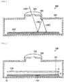
- FIG. 1 is a cross-sectional view of a schematic configuration example of a general imaging device.
- electromagnetic radiation is simply referred to as light.
- the light includes invisible light such as infrared rays (including far infrared rays), ultraviolet rays, and gamma rays, in addition to visible light.
- an imaging device 900 generally has a configuration in which an image sensor 910 is accommodated in a housing 901 provided with an aperture 903 for incident light L901 to enter, to reduce an influence caused by undesired light. Further, the aperture 903 of the housing 901 is provided with a lens 902, as an optical system for condensing the incident light L901.
- a black diffusion material is used on an inner wall of the housing 901 to reduce an artifact caused by reflected light L902 which has been reflected on the image sensor 910 further being reflected on the inner wall of the housing 901 (secondary reflected light L903) and re-entering the image sensor 910 (an artifact caused by secondary reflection).
- the artifact caused by the secondary reflection may be, for example, image disturbance attributed to a multi-layered image, ringing, or the like, which is caused by the light that has been reflected on the image sensor being reflected on a surrounding reflective member and re-entering the image sensor.
- the black diffusion material is used for the inner wall of the housing 901
- a degree of freedom in designing the image sensor 910 is limited and a manufacturing cost is increased.
- the incident light L901 is invisible light (e.g., infrared light), or for light that has been reflected on the lens 902, a filter, or the like.
- the incident light L901 is visible light and a coded aperture (also referred to as coded mask or binary mask) is used, it may be necessary that the coded aperture itself be manufactured using the black diffusion material, resulting in issues of increased manufacturing difficulty and an increased manufacturing cost.
- coded aperture also referred to as coded mask or binary mask
- a diffuser panel (also referred to as diffuser) is used as a configuration for reducing the artifact caused by secondary reflection.
- the use of the diffuser panel makes it possible to remarkably reduce the artifact caused by the secondary reflection even if a reflective member is disposed around the image sensor.
- the diffuser panel is disposed sufficiently close to a light reception surface of the image sensor, for example, such that light diffusion caused by the diffuser panel does not influence an image quality.
- incident light traveling toward the image sensor becomes light (hereinafter referred to as scattered light) whose diameter expands in accordance with a propagation distance by passing through the diffuser panel.
- scattered light whose diameter expands in accordance with a propagation distance by passing through the diffuser panel.
- the diffuser panel is disposed sufficiently close to the light reception surface of the image sensor such that the image formed on the light reception surface of the image sensor is not blurred.
- the light reception surface of the image sensor may be a surface where light entrance surfaces of light receiving elements each of which is included in a unit pixel to be described later are arranged.
- a distance from the diffuser panel to the reflective member is set such that an image of secondary reflected light, which is reflected on the image sensor and on the surrounding reflective member and re-enters the image sensor, is negligible. That is, the reflected light that has been reflected on the image sensor passes through the diffuser panel in a reverse direction, is reflected on the surrounding reflective member, passes through the diffuser panel again in a forward direction, and enters the image sensor; thus, setting the distance from the light reception surface of the image sensor 10 to the reflective member sufficiently long makes it possible to sufficiently expand the diameter of the secondary reflected light to reduce the intensity thereof before re-entering the image sensor. Thereby, the image of the secondary reflected light that enters the light reception surface is sufficiently blurred to be negligible, which makes it possible to reduce the artifact caused by the secondary reflection.
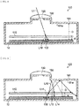
- FIG. 2 is a cross-sectional view illustrating a schematic configuration example of an imaging device according to the present embodiment.
- an imaging device 100 has a configuration in which an image sensor 10 is accommodated in a housing 101 provided with an aperture 103 for light L1 to enter. Further, a lens 102 is provided on the aperture 103 of the housing 101 as an optical system for condensing the light L1.
- the imaging device 100 includes a diffuser panel 110 disposed close to a light reception surface of the image sensor 10.
- the term "close to the light reception surface of the image sensor 10" may mean, for example, that it is closer to the light reception surface of the image sensor 10 than a top surface (hereinafter, also referred to as ceiling) 101a of an inner wall of the housing 101.
- light receiving elements (also referred to as light receivers) 132 each of which is included in a unit pixel 131 to be described later are arranged in a two-dimensional matrix in a row direction and a column direction.
- a distance from the light reception surface of the image sensor 10 to the top surface of the inner wall of the housing 101 is denoted by D
- a distance from the light reception surface of the image sensor 10 to the diffuser panel 110 is denoted by d.
- FIG. 2 and the following drawings illustrate that the top surface of the image sensor 10 and the light reception surface coincide with each other, they do not necessarily coincide with each other.
- the light receiving element 132 to be described later is formed at a predetermined depth from the top surface of the image sensor 10, or in a case where a microlens array or the like is provided on the top surface of the image sensor 10, the light reception surface of the image sensor 10 is at a position deeper than the top surface of the image sensor 10.
- light that has entered the image sensor 10 may be reflected not only on the light reception surface, but may also be reflected on the entrance surface of the light of the image sensor 10 itself.
- the light reception surface and the entrance surface are not distinguished from each other in order to simplify the description.
- the light to be detected by the image sensor 10 includes: visible light; and invisible light such as infrared rays (including far infrared rays), ultraviolet rays, and gamma rays.
- the image sensor 10 is configured as a sensor for visible light.
- the image sensor 10 includes, as a light receiving element, for example, an imaging element such as a photodiode that photoelectrically converts the light that has entered to generate electric charges.
- the image sensor 10 uses, as the light receiving element, a thermal infrared detection element such as a pyroelectric sensor, a thermopile, and a bolometer, or a cooled or uncooled quantum-type infrared detection element.
- a thermal infrared detection element such as a pyroelectric sensor, a thermopile, and a bolometer, or a cooled or uncooled quantum-type infrared detection element.
- FIG. 3 is a block diagram illustrating a schematic configuration example of an image sensor for the infrared light (including the far-infrared light) according to the first embodiment.
- an image sensor 10A for invisible light includes an element array 3, a signal processing circuit 5, and a controller 1.
- the element array 3 includes, for example, a plurality of light receiving elements 132 arranged in the two-dimensional matrix in the row direction and the column direction. In FIG. 3 , some of the rows and columns in the pixel array 13 are omitted for simplicity of the description; however, several tens to several thousands of light receiving elements 132 may be disposed in each row and each column, for example.
- the lens 102 is disposed at a position where an image of the light L1 is formed on the light reception surface on which the light receiving elements 132 are arranged.
- the controller 1 controls reading of an electric signal from the light receiving element 132. Specifically, the controller 1 causes the element array 3 to output, to the signal processing circuit 5, the electric signal generated by application of the light L1 to the light receiving element 132 for each element or for each row, for example.
- the controller 1 reads an electric signal indicating a difference in a resistance value due to a temperature increase in the light receiving element caused by absorbing the incident light from each of the light receiving elements 132 of the element array 3. Further, in the case where a thermopile is used as the light receiving element, the controller 1 reads an electric signal of a voltage value proportional to a local temperature difference or a temperature gradient caused by absorbing the incident light from each of the light receiving elements 132 of the element array 3.
- the signal processing circuit 5 processes the electric signal outputted from the element array 3 by the controller 1 to generate image data based on an infrared image.
- the thermal infrared detection element is used as the light receiving element 132
- the light receiving element 132 itself may include an AD (Analog-to-Digital) converter that converts an analog electric signal into a digital electric signal.
- the signal processing circuit 5 digitally processes the electric signal outputted from the element array 3 to generate the image data.
- the signal processing circuit 5 converts the analog electric signal outputted from the element array 3 into a digital value, and thereafter digitally processes the digital value to generate the image data.
- FIG. 4 is a block diagram illustrating a schematic configuration example of an image sensor for the visible light according to the first embodiment.
- an image sensor 10B for visible light includes a pixel array 13, a signal processing circuit 15, a reference voltage generator 17, and an output circuit 19.
- a driving controller is provided on an outer side of the pixel array 13 for sequentially reading analog pixel signals from respective unit pixels 131 and outputting the analog pixel signals as digital image data.
- the driving controller may include, for example, a horizontal transfer circuit 18, a pixel driving circuit 12, a timing control circuit 11, and the like.
- the pixel array 13 includes the plurality of unit pixels 131 arranged in the two-dimensional matrix in the row direction and the column direction. In FIG. 4 , some of the rows and columns in the pixel array 13 are omitted for simplicity of the description; however, several tens to several thousands of unit pixels 131 may be disposed in each row and each column, for example.
- Each unit pixel 131 includes, for example, a light receiving element such as a photodiode that photoelectrically converts the light that has entered to generate electric charges (for convenience of description, the reference numeral of the light receiving element is also denoted as "132"), and a pixel circuit that generates a pixel signal corresponding to an amount of electric charges generated in the light receiving element 132.
- a light receiving element such as a photodiode that photoelectrically converts the light that has entered to generate electric charges
- 132 the reference numeral of the light receiving element
- the pixel circuit includes, for example: a transfer transistor that transfers the electric charges generated in the light receiving element 132 to a predetermined node (floating diffusion region) functioning as an electric charge storage; a reset transistor that discharges the electric charges stored in the predetermined node and/or the light receiving element 132; an amplifier transistor that causes a pixel signal of a voltage value corresponding to the amount of electric charges stored in the predetermined node to appear in a vertical signal line VSL; and a selection transistor that switches a connection between the amplifier transistor and the vertical signal line VSL.
- a transfer transistor that transfers the electric charges generated in the light receiving element 132 to a predetermined node (floating diffusion region) functioning as an electric charge storage
- a reset transistor that discharges the electric charges stored in the predetermined node and/or the light receiving element 132
- an amplifier transistor that causes a pixel signal of a voltage value corresponding to the amount of electric charges stored in the predetermined node to appear in a vertical signal line VSL
- a selection transistor that switches a
- each unit pixel 131 is coupled to the pixel driving circuit 12 via a pixel drive line LD for pixel selection and to the signal processing circuit 15 via the vertical signal line VSL.
- the pixel drive line LD refers to all wiring lines that enter the respective unit pixels 131 from the pixel driving circuit 12.
- the pixel drive line LD may include a control line that propagates various pulse signals (e.g., pixel reset pulses, transfer pulses, drain line control pulses, etc.) for driving the unit pixel 131.
- the signal processing circuit 15 includes: an analog circuit such as an AD (Analog to Digital) converter that converts an analog pixel signal read from the unit pixel 131 into a digital pixel signal; and a logic circuit that performs a digital process such as a CDS (correlated double sampling) process on the basis of the pixel signal converted into a digital value by the AD converter.
- the AD converter may be provided on a one-to-one basis to each unit pixel 131, may be provided on a one-to-one basis to each pixel group including a plurality of unit pixels 131, or may be provided on a one-to-one basis to each column in the pixel array 13.
- the reference voltage generator 17 supplies the signal processing circuit 15 with a reference voltage REF for converting the analog pixel signal read from each unit pixel 131 via the vertical signal line VSL into the digital pixel signal.
- the timing control circuit 11 outputs an internal clock that is necessary for an operation of each section, a pulse signal that provides a timing at which each section starts its operation, and the like. Further, the timing control circuit 11 receives data that commands a master clock, an operation mode, etc. from an outside or outputs data that includes information of the image sensor 10B.
- the timing control circuit 11 outputs, to the pixel driving circuit 12, the pulse signal providing a timing for reading the pixel signal from each unit pixel 131. Further, timing control circuit 11 outputs, to the horizontal transfer circuit 18, a column address signal for sequentially reading pixel signals (digital voltage values) of signal components that have been AD-converted by the AD converter from the signal processing circuit 15 for each column.
- the timing control circuit 11 supplies, as the internal clock, a clock having the same frequency as a master clock inputted from the outside, a clock obtained by dividing the clock by two, a clock of a lower speed obtained by dividing the clock by a larger number, or the like, to each section in the image sensor 10B, for example, the horizontal transfer circuit 18, the pixel driving circuit 12, the signal processing circuit 15, and the like.
- a clock divided by two or a clock having a frequency lower than or equal to that of the clock divided by two are each collectively referred to as low-speed clock.
- the pixel driving circuit 12 selects a row of the pixel array 13 and outputs a pulse necessary for driving the row to the pixel drive line LD.
- the pixel driving circuit 12 includes a vertical decoder that defines a vertical read row (selecting a row of the pixel array 13) and a vertical driver that supplies a pulse to and drives the pixel drive line LD to the unit pixel 131 on a read address (row direction) defined by the vertical decoder. It is to be noted that the vertical decoder selects, in addition to a row from which the pixel signal is read, a row for an electronic shutter.
- the horizontal transfer circuit 18 performs, in accordance with the column address signal inputted from the timing control circuit 11, a shift operation (scanning) of reading a digital pixel signal from the AD converter of the read column specified by the column address signal to a horizontal signal line HSL.
- the output circuit 19 outputs the digital pixel signal read by the horizontal transfer circuit 18 to the outside as image data.
- the signal processing circuit 15 may include an AGC (Auto Gain Control) circuit having a signal-amplifying function as necessary.
- AGC Automatic Gain Control
- the image sensor 10B may be provided with a clock converter that generates a pulse having a clock frequency higher than the inputted clock frequency.
- the timing control circuit 11 may generate the internal clock on the basis of an input lock (e.g., a master clock) inputted from the outside or a high-speed clock generated by the clock converter.
- the image sensor 10B for visible light is not limited to the above-mentioned CMOS (Complementary Metal Oxide Semiconductor) type image sensor, and it is possible to apply various image sensors such as CCD (Charge Coupled Device) type, for example.
- CMOS Complementary Metal Oxide Semiconductor
- CCD Charge Coupled Device
- the diffuser panel 110 converts light that has entered into scattered light whose diameter expands in accordance with a propagation distance and outputs the scattered light, for example, with a predetermined scattering angle profile ⁇ ( ⁇ ).
- FIG. 5 is a diagram illustrating an example of a scattering angle profile of a diffuser panel according to the present embodiment. It is to be noted that the diffuser panel 110 according to the present embodiment includes, for example, a normalized circularly symmetric scattering angle profile ⁇ ( ⁇ ). Further, in FIG. 5 , a horizontal axis represents a deviation angle ⁇ from an optical axis of the incident light, and a vertical axis represents a light intensity of the scattered light outputted from the diffuser panel. It is to be noted that the incident light may be visible light or invisible light.
- the scattering angle profile ⁇ ( ⁇ ) of the diffuser panel 110 has a normalized circularly symmetric Gaussian distribution as illustrated in FIG. 5 .
- the diffuser panel 110 has a normalized circularly symmetric scattering angle profile, but the present disclosure is not limited thereto.
- various diffuser panels such as a diffuser panel provided with a scattering angle profile that is asymmetric with respect to the optical axis.
- the diffuser panel 110 a diffuser panel that diffuses light in a predetermined direction determined by designing in advance and outputs the light.
- a diffuser panel 110A that outputs the light L1 while diffusing the light L1 in a direction perpendicular to the light reception surface of the image sensor 10.
- the diffuser panel 110A makes it possible to improve a sensitivity of the image sensor 10. Further, as illustrated in FIG. 7 , the diffuser panel 110A is also able to diffuse light L11 reflected on the image sensor 10 and directed toward the lens 102, which makes it possible to reduce the artifact caused by the secondary reflection.
- FIG. 8 is a diagram for describing up to a moment when light that has entered the imaging device according to the present embodiment enters the light reception surface of the image sensor.
- FIG. 9 is a diagram for describing secondary reflected light in the imaging device according to the present embodiment. It is to be noted that FIG. 9 illustrates up to a moment when the light L11 that has been reflected on the image sensor 10 is reflected on the ceiling 101a of the housing 101 and re-enters the image sensor 10.
- the light L1 that has entered the inside of the housing 101 of the imaging device 100 via the lens 102 is converted into light (scattered light) L10 whose diameter expanded in accordance with a propagation distance by passing through the diffuser panel 110, and enters the image sensor 10.
- the distance e.g., the shortest distance
- the diffuser panel 110 e.g., the surface of the diffuser panel 110 which the incident light enters in the forward direction
- the diffuser panel 110 and the image sensor 10 close to each other to such an extent that the light L10 that has entered the diffuser panel 110 in the vicinity of the center of each light receiving element 132 and has diffused does not enter adjacent light receiving elements 132, it is possible to reduce the blurring of the image formed on the light reception surface and suppress deterioration of the image quality.
- the light receiving element 132 of the image sensor 10 is not a perfect absorber by itself, and reflects a portion of the light L10 that has entered.
- the light (reflected light) L11 that has been reflected on the image sensor 10 mainly passes through the diffuser panel 110 in the opposite direction, is reflected on the ceiling 101a of the housing 101, and then passes through the diffuser panel 110 and enters the image sensor 10 again.
- the light L11 that has been reflected on the image sensor 10 is converted into light L12 which is scattered light by passing through the diffuser panel 110 in the opposite direction.
- light L13 that has been reflected on the ceiling 101a of the housing 101 is converted into light L14 which is scattered light by passing through the diffuser panel 110 in the forward direction.
- a diameter of the light L14 that enters the light reception surface of the image sensor 10 by setting a length of, out of the optical path of the light L11 that is reflected on the image sensor 10 and re-enters the image sensor 10, at least the optical path (e.g., the optical path of the light L12 and L13 in FIG. 9 ) of the light that passes through the diffuser panel 110 in the opposite direction, is reflected on the ceiling 101a of the housing 101, and re-enters the diffuser panel 110 in the forward direction to be sufficiently long.
- the optical path e.g., the optical path of the light L12 and L13 in FIG. 9
- the distance (e.g., the shortest distance) D from the light reception surface of the image sensor 10 to the ceiling 101a of the housing 101 is sufficiently long, it is possible to sufficiently widen the diameter of the light L14 that enters the light reception surface.
- the intensity of the light L14 that enters the light reception surface which makes it possible to sufficiently blur the image of the light L14 that has entered to a negligible extent.
- the lower limit of the distance d from the light reception surface of the image sensor 10 to the diffuser panel 110 is determined depending on, for example, a manufacturing process of the image sensor 10. Therefore, in designing the imaging device 100, it is preferable to determine the distance d from the light reception surface of the image sensor 10 to the diffuser panel 110 first, and then select a diffuser panel 110 having a scattering angle profile that is able to sufficiently reduce the artifact caused by the secondary reflection.
- FIG. 10 is a schematic view for describing up to a moment when light that has entered the imaging device according to the present embodiment enters the image sensor via the diffuser panel.
- a scattering angle ⁇ be sufficiently small so that the relative light intensity P( ⁇ ) in the above Expression (2) approaches 1.
- the scattering angle ⁇ of the diffuser panel 110 may be set such that a radius r of a spot formed on the light reception surface of the image sensor 10 by half of the light L10 satisfies the following Expression (3).
- the pixel pitch may be the pitch of the light receiving elements 132.
- the pixel pitch may have a size, for example, equal to a size of the light receiving element 132.
- Expression (3) expresses a case where the light L1 enters perpendicularly to the diffuser panel 110.
- a shape and a size of the spot formed on the light reception surface of the image sensor 10 by the light L10 diffused by the diffuser panel 110 also depend on an incident angle ⁇ of the light L1 to the diffuser panel 110.
- a diameter of the spot formed by the light L10 on the light reception surface of the image sensor 10 is substantially proportional to d/cos ⁇ . This indicates that the larger the incident angle ⁇ , the more blurred is the image that the light L10 diffused by the diffuser panel 110 forms on the light reception surface of the image sensor 10.
- Expression (3) may be modified as in the following Expression (4).
- ⁇ is a maximum incident angle of the light L1.
- P ⁇ 2 ⁇ ⁇ 0 ⁇ ⁇ ⁇ ⁇ d ⁇ > 0.5
- ⁇ arctan r ⁇ cos max ⁇ d
- the diffuser panel 110 has a spatially non-uniform profile, that is, the smaller the incident angle ⁇ , the stronger the diffuser panel 110 diffuses the surrounding of the spot. Further, the diffuser panel 110 also has a function that the distance between the light reception surface of the image sensor 10 and the diffuser panel 110 varies depending on the incident angle ⁇ . That is, the larger the incident angle ⁇ , the shorter the distance from the light reception surface of the image sensor 10 to the diffuser panel 110.
- FIG. 11 is a schematic view for describing the artifact caused by the secondary reflection according to the present embodiment.
- the description ignores spreading of the light L13 that has been reflected on the ceiling 101a of the housing 101, the spreading being due to the diffusion caused by the diffuser panel 110 when the light L13 re-enters the image sensor 10. This is because the optical path length of the light that passes through the diffuser panel 110 and re-enters the image sensor 10 is sufficiently shorter than the optical path length of the light L13 that is reflected by the image sensor 10 and re-enters the image sensor 10, and even if the influence thereof is ignored, the result of the consideration is hardly influenced.
- a light propagation distance D' of the light L10 that is reflected on the image sensor 10 and re-enters the image sensor 10 is more than or equal to the distance obtained by subtracting the distance d from twice the distance D, that is, D' ⁇ D+(D-d).
- the diffuser panel 110 is disposed close to the light reception surface of the image sensor 10 accommodated in the housing 101. This makes it possible to sufficiently blur the image of the light L14 that is reflected on the image sensor 10 and on the surrounding reflective member (e.g., ceiling 101a) and re-enters the image sensor 10 to a negligible extent, thereby making it possible to reduce the artifact caused by the secondary reflection.
- the diffuser panel 110 is disposed sufficiently close to the light reception surface of the image sensor 10. This causes the blurring of the image of the light L10 formed on the light reception surface of the image sensor 10 to be reduced, which makes it possible to suppress deterioration of the image quality.
- the second embodiment will be described in detail by referring to the drawings.
- the first embodiment an example of the case has been described where the diffuser panel 110 is disposed close to a chip of the image sensor 10.
- the second embodiment will illustrate an example of a case where a diffuser panel is embedded in a chip of an image sensor.
- the image sensor 10 included in the imaging device 100 exemplified in the first embodiment is replaced by an image sensor 20 to be described later.
- the image sensor 20 may be a sensor for visible light or a sensor for invisible light.
- FIG. 12 is a schematic cross-sectional view illustrating a schematic configuration example of the image sensor according to the present embodiment. It is to be noted that FIG. 12 illustrates an example of a cross-sectional structure of one unit pixel in the image sensor 20. Further, FIG. 12 omits configurations of pixel circuits in the unit pixel, for example, a transfer transistor, a reset transistor, an amplifier transistor, a selection transistor, and the like.
- the image sensor 20 has a configuration in which a filter 23, a diffuser 210, and a light receiver 24 are formed on a semiconductor substrate 21 of a silicon substrate or the like, for example.
- a microlens 22 for each unit pixel is provided on a light entrance surface of the semiconductor substrate 21.
- the microlens 22 condenses, for example, light L2 that has entered on the light receiver 24.
- the filter 23 is provided with, for example, a wavelength selection function of transmitting light having a particular wavelength.
- the diffuser 210 diffuses light that has entered with a predetermined scattering angle profile and outputs scattered light L20, similarly to the diffuser panel 110 according to the embodiment described above.
- the light receiver 24 images light that has entered and generates electric charges, similarly to the light receiving element 132 according to the embodiment described above.
- the diffuser 210 is disposed, for example, between the filter 23 and the light receiver 24.
- the diffuser 210 is located immediately below the filter 23.
- the diffuser 210 is located on a reflective member such as a wiring line or the like formed on the element forming surface; thus, there is also an advantage that it becomes possible to reduce crosstalk due to reflection on the reflective member.
- FIG. 13 is a diagram for describing up to a moment when light that has been reflected on the entrance surface of the light receiver illustrated in FIG. 12 is outputted from the image sensor via the microlens.
- Light L21 that has been reflected on the entrance surface of the light receiver 24 is converted into scattered light L22 having a scattering angle ⁇ by passing through the diffuser 210 in the opposite direction, and then enters the microlens 22.
- the microlens 22 having a convex shape reduces the scattering angle ⁇ of the scattered light L22 that has entered using its light condensing function. Consequently, light L23 having a scattering angle ⁇ 1 smaller than the scattering angle ⁇ is outputted from the microlens 22.
- an exit surface of the light L23 in a case where it is assumed that there is no diffuser 210 is, for example, a surface separated from the optical center O of the microlens 22 by a distance I shorter than the focal distance F, from the following Expression (7) on the basis of a thin lens approximation.
- the distance I may be determined by the following Expression (8).
- I LF L ⁇ F
- the distance I is a negative value at all times, and the absolute value of the distance I is smaller than the distance L at all times.
- the exit surface of the light L23 in the case where it is assumed that there is no diffuser 210 is located between the light receiver 24 and the diffuser 210 which is located at the distance I determined by Expression (8).
- the scattering angle ⁇ 1 of the light L23 may be approximated by the following Expression (9). [Math. 9] L ⁇ sin ⁇ ⁇ I ⁇ sin ⁇ 1
- ⁇ 1 may be determined by the following Expression (10) on the basis of Expression (9). [Math. 10] L ⁇ ⁇ ⁇ I ⁇ ⁇ 1 ⁇ ⁇ 1 ⁇ L ⁇ ⁇ I
- the diffuser 210 is embedded in the chip of the image sensor 20, similarly to the first embodiment, it is possible to sufficiently blur the image of the light that has been reflected on the entrance surface of the light receiver 24 and on the surrounding reflective member (e.g., ceiling 101a) and has re-entered the light receiver 24 to a negligible extent, and it is possible to reduce blurring of the image of the light formed on the light receiver 24. This makes it possible to achieve reduction in the artifact caused by the secondary reflection and suppression of deterioration of the image quality.
- the diffuser 210 may be disposed between the filter 23 and the microlens 22.
- the filter 23 or the other member may be disposed between the diffuser 210 and the light receiver 24, which makes it possible to reduce blurring of the image formed on the light reception surface of the image sensor 20 and suppress the deterioration of the image quality, and additionally to reduce crosstalk between unit pixels that are adjacent to each other.
- the filter 23 and the diffuser 210 it is also possible to use a layer in which a filter and a diffuser are integrated. Also in this case, similarly to the above-described structure, it is possible to sufficiently shorten the distance d from the light entrance surface of the light receiver 24 to the diffuser 210, which makes it possible to reduce the blurring of the image formed on the light reception surface of the image sensor 20 and suppress the deterioration of the image quality.
- the imaging device 100 includes the lens 102.
- the third embodiment will illustrate an example of a case where an imaging device includes a coded aperture as an optical system in place of the lens 102.
- the coded aperture is a mask-shape member provided with an optical aperture having a random shape which is not geometric or circular.
- the coded aperture is a diaphragm portion used in a coding imaging technique to adjust a brightness, a depth of field, and the like of an image by controlling PSF (point spread function).
- the coded aperture materials having a high light-absorbing property are not necessarily used because of its easiness of processing, cost, and the like.
- the coded aperture has high reflectivity, as illustrated in FIG. 14 , the light L902 that has been reflected on the image sensor 910 is reflected on a coded aperture 912 with high reflectance and re-enters the image sensor 910.
- an artifact caused by the secondary reflection attributed to reflected light L913 having a high light intensity strongly appears in the image captured by the image sensor 910.
- a diffuser panel is disposed sufficiently close to the light reception surface of the image sensor.
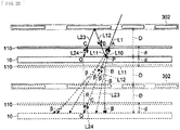
- FIG. 15 is a cross-sectional view illustrating a schematic configuration example of the imaging device according to the present embodiment.
- an imaging device 300 includes, for example, a configuration in which the diffuser panel 110 is disposed between the image sensor 10 and a coded aperture 302 which is located on a light reception surface side of the image sensor 10.
- the image sensor 10 may be similar to, for example, the image sensor 10 illustrated in the first embodiment or the image sensor 20 illustrated in the second embodiment.
- the light L1 entered from the optical aperture of the coded aperture 302 is diffused by the diffuser panel 110 and enters the image sensor 10 as the light L10.
- the diffuser panel 110 is disposed close to the light reception surface of the image sensor 10. This makes it possible to reduce blurring of the image formed on the light reception surface and suppress deterioration of the image quality.
- the light L11 that has been reflected on the image sensor 10 is converted into the light L12 whose diameter expands in accordance with a propagation distance by passing through the diffuser panel 110 in the opposite direction.
- the light L12 is reflected on a light-shielding portion of the coded aperture 302 and returns to the diffuser panel 110. Accordingly, accordingly, an image of the light L23 (oblique line portion in FIG. 17 ) that re-enters the diffuser panel 110 in the forward direction is an image obtained by enlarging a pattern of the coded aperture 302.
- FIG. 18 is a diagram for describing traveling of light that has entered an imaging device including no diffuser panel.
- FIG. 19 is a diagram for describing traveling of light that has entered an imaging device including a diffuser panel.
- FIG. 20 is a diagram for describing traveling of light that has passed through a diffuser panel. It is to be noted that in FIGs. 18 to 20 , configurations indicated by broken lines indicate traveling of light in a case where a reflection optical system is replaced with a transmission optical system. Further, in FIGs. 18 to 20 , for example, a pixel pitch 2r of the image sensor 10 is set to 0.00001 m, and the distance D from the light reception surface of the image sensor 10 to the coded aperture 302 is set to 0.01 m. Moreover, in FIGs.
- the light L1 that has entered via the optical aperture of the coded aperture 302 enters a point P on the light reception surface of the image sensor 10. Further, light L92 that has been reflected at the point P is reflected on the light-shielding portion of the coded aperture 302, and light L93 obtained by this reflection enters a point Q on the light reception surface of the image sensor 10. Thus, spots of light formed on the light reception surface of the image sensor 10 are two points P and Q.
- the diffuser panel 110 In contrast, in the case where the diffuser panel 110 is provided, as illustrated in FIG. 19 , the light L1 that has entered via the optical aperture of the coded aperture 302 enters the diffuser panel 110 at a point A in the forward direction and diffuses, thereby being uniformly converted into the light L10 which is scattered light having a spread angle 2 ⁇ . Thereafter, the light L10 forms a spot approximately centered on the point P on the light reception surface of the image sensor 10.
- the light L11 diffused at the point A and reflected on the light reception surface of the image sensor 10 thereafter enters in the opposite direction the diffuser panel 110 at a point B and is diffused to be converted into the light L12, and is further reflected on the light-shielding portion of the coded aperture 302.
- the light L23 reflected on the light-shielding portion enters in the forward direction the diffuser panel 110 at a point C and is diffused to be converted into light L24.
- the light L24 forms a spot having a remarkably large diameter approximately centered on the point Q on the light reception surface of the image sensor 10.
- the secondary reflected light (corresponding to L24) that re-enters the image sensor 10 is diffused by the diffuser panel 110 two or more times (three times in this example). Accordingly, it becomes possible to expand the diameter of the spot formed on the light reception surface of the image sensor 10 by the secondary reflected light and to blur the image, which makes it possible to further reduce the artifact caused by the secondary reflection.
- the coded aperture 302 is used instead of the lens 102, similarly to the first embodiment, it is possible to sufficiently blur the image of the light L23 that has been reflected on the image sensor 10 and on the surrounding reflective member (e.g., coded aperture 302) and has re-entered the image sensor 10 to a negligible extent, by disposing the diffuser panel 110 close to the light reception surface of the image sensor 10. This makes it possible to reduce the artifact caused by the secondary reflection.
- the present technology may have the following configurations.
- An imaging device including:
- the imaging device in which the diffuser converts the incident light into the scattered light to cause a size of a spot formed on an entrance surface of light of the light receiver by at least half of the scattered light to be smaller than a size of the entrance surface of the light receiver.
- the imaging device in which a size of the light receiver is 2r or more.
- the imaging device according to any one of (1) to (4), in which the light receiver is an infrared detection element that receives an infrared ray and converts the infrared ray into an electric signal.
- the light receiver is an infrared detection element that receives an infrared ray and converts the infrared ray into an electric signal.
- the imaging device in which the infrared detection element is any one of a pyroelectric sensor, a thermopile, and a bolometer.
- the imaging device according to any one of (1) to (6), further including an optical system through which the incident light passes, in which the diffuser is closer to the light receiver than to the optical system.
- the imaging device in which the optical system is a lens that condenses the incident light.
- the imaging device in which the optical system is a coded aperture.
- the imaging device according to any one of (1) to (9), further including a microlens that is provided on a one-to-one basis to the light receiver, and condenses light that enters the light receiver.
- the imaging device according to any one of (1) to (10), further including a filter that limits light that enters the light receiver to light having a particular wavelength.
- the imaging device in which the diffuser is disposed between the light receiver and the filter.
- the imaging device in which the diffuser is disposed on an opposite side to the light receiver with the filter interposed therebetween.
- the imaging device according to any one of (1) to (10), in which the diffuser limits light that enters the light receiver to light having a particular wavelength.
- a solid-state imaging device including:
Landscapes
- Physics & Mathematics (AREA)
- General Physics & Mathematics (AREA)
- Spectroscopy & Molecular Physics (AREA)
- Multimedia (AREA)
- Signal Processing (AREA)
- Engineering & Computer Science (AREA)
- Health & Medical Sciences (AREA)
- Toxicology (AREA)
- Optics & Photonics (AREA)
- Solid State Image Pick-Up Elements (AREA)
- Transforming Light Signals Into Electric Signals (AREA)
- Photometry And Measurement Of Optical Pulse Characteristics (AREA)
- Light Receiving Elements (AREA)
Applications Claiming Priority (2)
| Application Number | Priority Date | Filing Date | Title |
|---|---|---|---|
| JP2018197319 | 2018-10-19 | ||
| PCT/JP2019/033232 WO2020079960A1 (fr) | 2018-10-19 | 2019-08-26 | Dispositif d'imagerie et dispositif d'imagerie à semi-conducteurs |
Publications (2)
| Publication Number | Publication Date |
|---|---|
| EP3869794A1 true EP3869794A1 (fr) | 2021-08-25 |
| EP3869794A4 EP3869794A4 (fr) | 2022-04-20 |
Family
ID=70284567
Family Applications (1)
| Application Number | Title | Priority Date | Filing Date |
|---|---|---|---|
| EP19873204.2A Withdrawn EP3869794A4 (fr) | 2018-10-19 | 2019-08-26 | Dispositif d'imagerie et dispositif d'imagerie à semi-conducteurs |
Country Status (5)
| Country | Link |
|---|---|
| US (1) | US11546530B2 (fr) |
| EP (1) | EP3869794A4 (fr) |
| JP (1) | JPWO2020079960A1 (fr) |
| CN (1) | CN113170062A (fr) |
| WO (1) | WO2020079960A1 (fr) |
Families Citing this family (3)
| Publication number | Priority date | Publication date | Assignee | Title |
|---|---|---|---|---|
| WO2020079960A1 (fr) * | 2018-10-19 | 2020-04-23 | ソニー株式会社 | Dispositif d'imagerie et dispositif d'imagerie à semi-conducteurs |
| DE102019123404B4 (de) * | 2019-09-02 | 2024-02-15 | Bayerische Motoren Werke Aktiengesellschaft | Sensorvorrichtung und Fahrassistenzsystem |
| JPWO2022202054A1 (fr) * | 2021-03-26 | 2022-09-29 |
Family Cites Families (16)
| Publication number | Priority date | Publication date | Assignee | Title |
|---|---|---|---|---|
| JP2004266250A (ja) * | 2003-02-12 | 2004-09-24 | Inter Action Corp | 固体撮像素子の試験装置、中継装置および光学モジュール |
| US20060214673A1 (en) | 2003-11-28 | 2006-09-28 | Shingo Tamai | Intrument for testing solid-state imaging device |
| US7738026B2 (en) | 2005-05-02 | 2010-06-15 | Andrew G. Cartlidge | Increasing fill-factor on pixelated sensors |
| JP4521660B2 (ja) | 2004-05-20 | 2010-08-11 | 株式会社ニコン | 照明補助装置及びこの照明補助装置を用いた検査装置 |
| JP2007047757A (ja) * | 2005-07-13 | 2007-02-22 | Sony Corp | 透過型スクリーンの製造方法、その製造装置および透過型スクリーン |
| US7423821B2 (en) | 2006-03-24 | 2008-09-09 | Gentex Corporation | Vision system |
| US9891098B2 (en) | 2010-12-30 | 2018-02-13 | Apple Inc. | Diffuser and filter structures for light sensors |
| US8779540B2 (en) | 2011-01-26 | 2014-07-15 | Maxim Integrated Products, Inc. | Light sensor having transparent substrate with lens formed therein |
| US8969808B2 (en) | 2012-06-19 | 2015-03-03 | Amphenol Thermometrics, Inc. | Non-dispersive infrared sensor with a reflective diffuser |
| US9405124B2 (en) * | 2013-04-09 | 2016-08-02 | Massachusetts Institute Of Technology | Methods and apparatus for light field projection |
| CN105593651B (zh) | 2013-08-02 | 2019-06-07 | 威利食品有限公司 | 光谱测定系统和方法、光谱设备和系统 |
| US9645008B2 (en) | 2014-08-25 | 2017-05-09 | Apple Inc. | Light sensor windows for electronic devices |
| EP3032583B1 (fr) | 2014-12-08 | 2020-03-04 | ams AG | Capteur optique intégré et procédé de production associé |
| CN106170052B (zh) * | 2015-05-22 | 2020-11-06 | 微软技术许可有限责任公司 | 双传感器超光谱运动成像系统 |
| US10783652B2 (en) * | 2016-05-06 | 2020-09-22 | Arizona Board Of Regents On Behalf Of The University Of Arizona | Plenoptic imaging apparatus, method, and applications |
| WO2020079960A1 (fr) * | 2018-10-19 | 2020-04-23 | ソニー株式会社 | Dispositif d'imagerie et dispositif d'imagerie à semi-conducteurs |
-
2019
- 2019-08-26 WO PCT/JP2019/033232 patent/WO2020079960A1/fr not_active Ceased
- 2019-08-26 CN CN201980067143.5A patent/CN113170062A/zh not_active Withdrawn
- 2019-08-26 JP JP2020552560A patent/JPWO2020079960A1/ja not_active Abandoned
- 2019-08-26 US US17/284,600 patent/US11546530B2/en active Active
- 2019-08-26 EP EP19873204.2A patent/EP3869794A4/fr not_active Withdrawn
Also Published As
| Publication number | Publication date |
|---|---|
| EP3869794A4 (fr) | 2022-04-20 |
| WO2020079960A1 (fr) | 2020-04-23 |
| US11546530B2 (en) | 2023-01-03 |
| JPWO2020079960A1 (ja) | 2021-09-30 |
| US20210258517A1 (en) | 2021-08-19 |
| CN113170062A (zh) | 2021-07-23 |
Similar Documents
| Publication | Publication Date | Title |
|---|---|---|
| KR102088401B1 (ko) | 이미지 센서 및 이를 포함하는 촬상 장치 | |
| US10728506B2 (en) | Optical filter, solid state imaging device, and electronic apparatus | |
| EP3869794A1 (fr) | Dispositif d'imagerie et dispositif d'imagerie à semi-conducteurs | |
| US8975594B2 (en) | Mixed-material multispectral staring array sensor | |
| EP3718299B1 (fr) | Optique unique pour imagerie de bas niveau de lumière et de haut niveau de lumière | |
| US20180156659A1 (en) | Waveguide Diffuser for Light Detection using an Aperture | |
| US10644050B2 (en) | Image sensor having micro lenses arranged in different periods | |
| US10404925B2 (en) | Chip scale multispectral imaging and ranging | |
| US10110811B2 (en) | Imaging module and imaging device | |
| JP2012160783A (ja) | 固体撮像装置およびカメラ | |
| US11658195B2 (en) | Image sensor including microlenses having different shapes | |
| US20100171865A1 (en) | Solid-state image-taking apparatus, manufacturing method thereof, and camera | |
| CN117561603A (zh) | 具有近红外吸收器的成像传感器 | |
| EP2061235B1 (fr) | Procédé de correction de sensibilité et dispositif imageur | |
| US12484326B2 (en) | Imaging array with directional response | |
| WO2019026600A1 (fr) | Module d'appareil photographique et dispositif de capture d'image | |
| CN114402226A (zh) | 光学传感器 | |
| US12299946B2 (en) | Highly efficient active illumination imaging systems and methods | |
| Shashkin et al. | The detector array system for 3-mm wavelength video imaging | |
| RU2709459C1 (ru) | Устройство компьютерной системы панорамного телевизионного наблюдения | |
| US20080231971A1 (en) | 3-Dimensional Image Detector | |
| US10763295B2 (en) | Imaging apparatus and electronic device | |
| Soldatov | An analysis of images of rapidly traveling objects by means of optoelectronic devices | |
| KR20250013177A (ko) | 미광(Stray light) 감소 시스템을 갖는 라이다(LIDAR) 유닛 | |
| KR20250113101A (ko) | 라이다 장치 |
Legal Events
| Date | Code | Title | Description |
|---|---|---|---|
| STAA | Information on the status of an ep patent application or granted ep patent |
Free format text: STATUS: THE INTERNATIONAL PUBLICATION HAS BEEN MADE |
|
| PUAI | Public reference made under article 153(3) epc to a published international application that has entered the european phase |
Free format text: ORIGINAL CODE: 0009012 |
|
| STAA | Information on the status of an ep patent application or granted ep patent |
Free format text: STATUS: REQUEST FOR EXAMINATION WAS MADE |
|
| 17P | Request for examination filed |
Effective date: 20210329 |
|
| AK | Designated contracting states |
Kind code of ref document: A1 Designated state(s): AL AT BE BG CH CY CZ DE DK EE ES FI FR GB GR HR HU IE IS IT LI LT LU LV MC MK MT NL NO PL PT RO RS SE SI SK SM TR |
|
| RIC1 | Information provided on ipc code assigned before grant |
Ipc: H01L 27/146 20060101ALI20211208BHEP Ipc: G02B 5/02 20060101ALI20211208BHEP Ipc: G02B 27/00 20060101ALI20211208BHEP Ipc: H04N 5/33 20060101ALI20211208BHEP Ipc: H01L 31/0232 20140101ALI20211208BHEP Ipc: H04N 5/369 20110101ALI20211208BHEP Ipc: G01J 5/10 20060101ALI20211208BHEP Ipc: G01J 5/08 20060101ALI20211208BHEP Ipc: G01J 5/06 20060101ALI20211208BHEP Ipc: G01J 5/00 20060101ALI20211208BHEP Ipc: G01J 1/04 20060101ALI20211208BHEP Ipc: G01J 1/02 20060101AFI20211208BHEP |
|
| DAV | Request for validation of the european patent (deleted) | ||
| DAX | Request for extension of the european patent (deleted) | ||
| A4 | Supplementary search report drawn up and despatched |
Effective date: 20220318 |
|
| RIC1 | Information provided on ipc code assigned before grant |
Ipc: H01L 27/146 20060101ALI20220314BHEP Ipc: G02B 5/02 20060101ALI20220314BHEP Ipc: G02B 27/00 20060101ALI20220314BHEP Ipc: H04N 5/33 20060101ALI20220314BHEP Ipc: H01L 31/0232 20140101ALI20220314BHEP Ipc: H04N 5/369 20110101ALI20220314BHEP Ipc: G01J 5/10 20060101ALI20220314BHEP Ipc: G01J 5/08 20060101ALI20220314BHEP Ipc: G01J 5/06 20060101ALI20220314BHEP Ipc: G01J 5/00 20060101ALI20220314BHEP Ipc: G01J 1/04 20060101ALI20220314BHEP Ipc: G01J 1/02 20060101AFI20220314BHEP |
|
| STAA | Information on the status of an ep patent application or granted ep patent |
Free format text: STATUS: THE APPLICATION HAS BEEN WITHDRAWN |
|
| 18W | Application withdrawn |
Effective date: 20220628 |