EP3887463B1 - Couches métalliques conductrices transparentes - Google Patents
Couches métalliques conductrices transparentes Download PDFInfo
- Publication number
- EP3887463B1 EP3887463B1 EP19892623.0A EP19892623A EP3887463B1 EP 3887463 B1 EP3887463 B1 EP 3887463B1 EP 19892623 A EP19892623 A EP 19892623A EP 3887463 B1 EP3887463 B1 EP 3887463B1
- Authority
- EP
- European Patent Office
- Prior art keywords
- metal
- substrate
- crystal growth
- ink
- growth ink
- Prior art date
- Legal status (The legal status is an assumption and is not a legal conclusion. Google has not performed a legal analysis and makes no representation as to the accuracy of the status listed.)
- Active
Links
Images


Classifications
-
- C—CHEMISTRY; METALLURGY
- C09—DYES; PAINTS; POLISHES; NATURAL RESINS; ADHESIVES; COMPOSITIONS NOT OTHERWISE PROVIDED FOR; APPLICATIONS OF MATERIALS NOT OTHERWISE PROVIDED FOR
- C09D—COATING COMPOSITIONS, e.g. PAINTS, VARNISHES OR LACQUERS; FILLING PASTES; CHEMICAL PAINT OR INK REMOVERS; INKS; CORRECTING FLUIDS; WOODSTAINS; PASTES OR SOLIDS FOR COLOURING OR PRINTING; USE OF MATERIALS THEREFOR
- C09D5/00—Coating compositions, e.g. paints, varnishes or lacquers, characterised by their physical nature or the effects produced; Filling pastes
- C09D5/24—Electrically-conducting paints
-
- C—CHEMISTRY; METALLURGY
- C09—DYES; PAINTS; POLISHES; NATURAL RESINS; ADHESIVES; COMPOSITIONS NOT OTHERWISE PROVIDED FOR; APPLICATIONS OF MATERIALS NOT OTHERWISE PROVIDED FOR
- C09D—COATING COMPOSITIONS, e.g. PAINTS, VARNISHES OR LACQUERS; FILLING PASTES; CHEMICAL PAINT OR INK REMOVERS; INKS; CORRECTING FLUIDS; WOODSTAINS; PASTES OR SOLIDS FOR COLOURING OR PRINTING; USE OF MATERIALS THEREFOR
- C09D11/00—Inks
- C09D11/02—Printing inks
- C09D11/03—Printing inks characterised by features other than the chemical nature of the binder
- C09D11/033—Printing inks characterised by features other than the chemical nature of the binder characterised by the solvent
-
- B—PERFORMING OPERATIONS; TRANSPORTING
- B05—SPRAYING OR ATOMISING IN GENERAL; APPLYING FLUENT MATERIALS TO SURFACES, IN GENERAL
- B05D—PROCESSES FOR APPLYING FLUENT MATERIALS TO SURFACES, IN GENERAL
- B05D3/00—Pretreatment of surfaces to which liquids or other fluent materials are to be applied; After-treatment of applied coatings, e.g. intermediate treating of an applied coating preparatory to subsequent applications of liquids or other fluent materials
- B05D3/14—Pretreatment of surfaces to which liquids or other fluent materials are to be applied; After-treatment of applied coatings, e.g. intermediate treating of an applied coating preparatory to subsequent applications of liquids or other fluent materials by electrical means
- B05D3/141—Plasma treatment
- B05D3/145—After-treatment
-
- C—CHEMISTRY; METALLURGY
- C09—DYES; PAINTS; POLISHES; NATURAL RESINS; ADHESIVES; COMPOSITIONS NOT OTHERWISE PROVIDED FOR; APPLICATIONS OF MATERIALS NOT OTHERWISE PROVIDED FOR
- C09D—COATING COMPOSITIONS, e.g. PAINTS, VARNISHES OR LACQUERS; FILLING PASTES; CHEMICAL PAINT OR INK REMOVERS; INKS; CORRECTING FLUIDS; WOODSTAINS; PASTES OR SOLIDS FOR COLOURING OR PRINTING; USE OF MATERIALS THEREFOR
- C09D1/00—Coating compositions, e.g. paints, varnishes or lacquers, based on inorganic substances
-
- C—CHEMISTRY; METALLURGY
- C09—DYES; PAINTS; POLISHES; NATURAL RESINS; ADHESIVES; COMPOSITIONS NOT OTHERWISE PROVIDED FOR; APPLICATIONS OF MATERIALS NOT OTHERWISE PROVIDED FOR
- C09D—COATING COMPOSITIONS, e.g. PAINTS, VARNISHES OR LACQUERS; FILLING PASTES; CHEMICAL PAINT OR INK REMOVERS; INKS; CORRECTING FLUIDS; WOODSTAINS; PASTES OR SOLIDS FOR COLOURING OR PRINTING; USE OF MATERIALS THEREFOR
- C09D11/00—Inks
- C09D11/02—Printing inks
- C09D11/03—Printing inks characterised by features other than the chemical nature of the binder
- C09D11/037—Printing inks characterised by features other than the chemical nature of the binder characterised by the pigment
-
- C—CHEMISTRY; METALLURGY
- C09—DYES; PAINTS; POLISHES; NATURAL RESINS; ADHESIVES; COMPOSITIONS NOT OTHERWISE PROVIDED FOR; APPLICATIONS OF MATERIALS NOT OTHERWISE PROVIDED FOR
- C09D—COATING COMPOSITIONS, e.g. PAINTS, VARNISHES OR LACQUERS; FILLING PASTES; CHEMICAL PAINT OR INK REMOVERS; INKS; CORRECTING FLUIDS; WOODSTAINS; PASTES OR SOLIDS FOR COLOURING OR PRINTING; USE OF MATERIALS THEREFOR
- C09D11/00—Inks
- C09D11/30—Inkjet printing inks
- C09D11/32—Inkjet printing inks characterised by colouring agents
- C09D11/322—Pigment inks
-
- C—CHEMISTRY; METALLURGY
- C09—DYES; PAINTS; POLISHES; NATURAL RESINS; ADHESIVES; COMPOSITIONS NOT OTHERWISE PROVIDED FOR; APPLICATIONS OF MATERIALS NOT OTHERWISE PROVIDED FOR
- C09D—COATING COMPOSITIONS, e.g. PAINTS, VARNISHES OR LACQUERS; FILLING PASTES; CHEMICAL PAINT OR INK REMOVERS; INKS; CORRECTING FLUIDS; WOODSTAINS; PASTES OR SOLIDS FOR COLOURING OR PRINTING; USE OF MATERIALS THEREFOR
- C09D11/00—Inks
- C09D11/30—Inkjet printing inks
- C09D11/36—Inkjet printing inks based on non-aqueous solvents
-
- C—CHEMISTRY; METALLURGY
- C09—DYES; PAINTS; POLISHES; NATURAL RESINS; ADHESIVES; COMPOSITIONS NOT OTHERWISE PROVIDED FOR; APPLICATIONS OF MATERIALS NOT OTHERWISE PROVIDED FOR
- C09D—COATING COMPOSITIONS, e.g. PAINTS, VARNISHES OR LACQUERS; FILLING PASTES; CHEMICAL PAINT OR INK REMOVERS; INKS; CORRECTING FLUIDS; WOODSTAINS; PASTES OR SOLIDS FOR COLOURING OR PRINTING; USE OF MATERIALS THEREFOR
- C09D11/00—Inks
- C09D11/52—Electrically conductive inks
-
- C—CHEMISTRY; METALLURGY
- C23—COATING METALLIC MATERIAL; COATING MATERIAL WITH METALLIC MATERIAL; CHEMICAL SURFACE TREATMENT; DIFFUSION TREATMENT OF METALLIC MATERIAL; COATING BY VACUUM EVAPORATION, BY SPUTTERING, BY ION IMPLANTATION OR BY CHEMICAL VAPOUR DEPOSITION, IN GENERAL; INHIBITING CORROSION OF METALLIC MATERIAL OR INCRUSTATION IN GENERAL
- C23C—COATING METALLIC MATERIAL; COATING MATERIAL WITH METALLIC MATERIAL; SURFACE TREATMENT OF METALLIC MATERIAL BY DIFFUSION INTO THE SURFACE, BY CHEMICAL CONVERSION OR SUBSTITUTION; COATING BY VACUUM EVAPORATION, BY SPUTTERING, BY ION IMPLANTATION OR BY CHEMICAL VAPOUR DEPOSITION, IN GENERAL
- C23C18/00—Chemical coating by decomposition of either liquid compounds or solutions of the coating forming compounds, without leaving reaction products of surface material in the coating; Contact plating
- C23C18/02—Chemical coating by decomposition of either liquid compounds or solutions of the coating forming compounds, without leaving reaction products of surface material in the coating; Contact plating by thermal decomposition
- C23C18/08—Chemical coating by decomposition of either liquid compounds or solutions of the coating forming compounds, without leaving reaction products of surface material in the coating; Contact plating by thermal decomposition characterised by the deposition of metallic material
-
- C—CHEMISTRY; METALLURGY
- C23—COATING METALLIC MATERIAL; COATING MATERIAL WITH METALLIC MATERIAL; CHEMICAL SURFACE TREATMENT; DIFFUSION TREATMENT OF METALLIC MATERIAL; COATING BY VACUUM EVAPORATION, BY SPUTTERING, BY ION IMPLANTATION OR BY CHEMICAL VAPOUR DEPOSITION, IN GENERAL; INHIBITING CORROSION OF METALLIC MATERIAL OR INCRUSTATION IN GENERAL
- C23C—COATING METALLIC MATERIAL; COATING MATERIAL WITH METALLIC MATERIAL; SURFACE TREATMENT OF METALLIC MATERIAL BY DIFFUSION INTO THE SURFACE, BY CHEMICAL CONVERSION OR SUBSTITUTION; COATING BY VACUUM EVAPORATION, BY SPUTTERING, BY ION IMPLANTATION OR BY CHEMICAL VAPOUR DEPOSITION, IN GENERAL
- C23C18/00—Chemical coating by decomposition of either liquid compounds or solutions of the coating forming compounds, without leaving reaction products of surface material in the coating; Contact plating
- C23C18/14—Decomposition by irradiation, e.g. photolysis, particle radiation or by mixed irradiation sources
- C23C18/145—Radiation by charged particles, e.g. electron beams or ion irradiation
Definitions
- the present disclosure relates generally to properties and methods for the formation of transparent conductive metal layers (TCML) on various surfaces using plasma.
- TCML transparent conductive metal layers
- Patent Application No. WO 2018/049322 teaches a method for forming a metal active component in a hybrid material. The method includes applying a metal precursor formulation on a substrate and exposing the metal precursor formulation applied on the substrate to a low-energy plasma. The low-energy plasma is operated according to a set of exposure parameters.
- WO 2018/140430 teaches a method for forming a crystalline metal layer on a three-dimensional (3D) substrate.
- the method of WO 2018/140430 comprises a step of applying a crystal growth ink to a surface of the 3D substrate.
- the crystal growth ink comprises a metal ionic precursor and a structuring liquid.
- the method further comprises a step of exposing the 3D substrate to plasma irradiation in a vacuum chamber to cause the growing of a crystalline metal layer on the 3D substrate.
- US Patent Application No. US 2017/0218218 relates to an ink composition for forming a patterned thin metal film on a substrate.
- the ink composition comprises metal cations and at least one solvent.
- US 2017/0218218 further discloses the patterned thin metal film is adhered to a surface of the substrate upon exposure of the metal cations to a low-energy plasma.
- US Patent Application No. US 2018/297387 relates to a method for directly writing metal traces on a wide range of substrate materials.
- the method of US 2018/297387 comprises a step of writing a pattern of particle-free metal-salt-based ink on the substrate material.
- the method further comprises a plasma-based treatment to remove non-metallic components of the ink and to decompose the metal salt into a pure metal.
- a method for depositing metals, metal blends and alloys onto substrate surfaces is described in US Patent Application No. US 2007/184208 .
- the method in US 2007/184208 discloses a step of selecting a porous substrate having open voids exposed to a surface of the porous substrate.
- the method further comprises selecting a precursor selected from a monomer or a comonomer and having a metallic component.
- a solution comprising the precursor dissolved in a liquid solvent is coated on the porous substrate.
- the method further comprises the removal of the liquid solvent, enabling the formation of a porous substrate coated with a dry deposit.
- the coated substrate is then introduced into a plasma reaction chamber comprising spaced apart electrodes.
- Radio frequency (RF) energy is applied across the electrodes, resulting in the formation of a plasma glow in the plasma reaction chamber.
- a plasma supporting gas is introduced into the plasma reaction chamber.
- the plasma glow leads to a conversion of the precursor to a dissociated form, enabling the formation of a deposit comprising the metallic component in elemental form as a cohesive film on the substrate surface.
- Conductive transparent films are a necessary component in many applications, including lighting, displays, solar cells, touchscreens and others.
- ITO Indium tin oxide
- Conventional fabrication techniques typically involve magnetron sputtering of the film, which is a very inefficient process with only a fraction of planar target material available for deposition on the substrate.
- the target material used for sputtering is very expensive.
- the industrial sputter deposition process of transparent conductive oxides is a great challenge because film thickness, optical properties, and electrical properties have to be distributed uniformly over a large substrate size at the same time.
- Optimum resistivity and transmittance cannot be reached at the same time and often the process control is very challenging and the parameters of the power supply alone are not suitable to control this process, resulting in a very narrow process window.
- the very narrow process window can also be an obstacle if large area uniformity is required. It is very difficult to adjust all process parameters such as partial pressures, pumping speed, magnetic field, and oxidation state to achieve uniformity along a large target.
- the invention is defined by the method of claim 1.
- a method for growing a transparent conductive metal layer on a substrate is taught in this disclosure.
- the method comprises the steps of activating the substrate using plasma irradiation for a predetermined amount of time, followed by applying crystal growth ink to a surface of the substrate, wherein the crystal growth ink includes a metal ionic precursor.
- the substrate is a PET substrate.
- the crystal growth ink comprises a structuring liquid component and a spreading liquid component, both of which are an organic solvent or a combination of organic solvents.
- the method further comprises a step of exposing the substrate to plasma irradiation to cause the growing of the transparent conductive metal layer comprised of a crystalline metal framework on the substrate, wherein the exposure is based on a set of predefined exposure parameters.
- the set of predefined exposure parameters comprises RF frequency of 13.56 MHz, 150 W of power, and 30 SCCM gas flow rate.
- the metal ionic precursor is silver nitrate with a concentration of 5 wt. % of the crystal growth ink.
- the formed conductive metal layer has a resistivity of 4 ohm/sq and transparency of 50%.
- the crystalline metal framework comprises large crystalline metal dendritic flakes each having a crystal node in the center.
- the set of predefined exposure parameters comprises RF frequency of 40 kHz, 150 W of power, and 30 SCCM gas flow rate.
- the metal ionic precursor is silver nitrate with a concentration of 3.5 wt. % of the crystal growth ink.
- the formed conductive metal layer has a resistivity of 15 ohm/sq and transparency of 80%.
- the crystalline metal framework comprises a randomized interconnected network of metal nanocrystals.
- the set of predefined exposure parameters may comprise for example an exposure to plasma at a pressure ranging from atmospheric of 1 ⁇ 10 5 Pa to medium vacuum of 1 ⁇ 10 -1 Pa.
- the crystal growth ink comprises for example the metal ionic precursor at a concentration between 0.01% and 20% by weight of the crystal growth ink.
- the crystal growth ink may further be any one of: a solution, a dispersion, a suspension, a gel, and a colloid.
- the metal ionic precursor may comprise a mixture of salts including one or more metal cations and counterions.
- the metal cations are stabilized for example by any one of a counterion and a ligand, wherein the stabilized metal cations form in one aspect an organometallic complex, such that the resulting salt is connected by coordinate bonds rather than by ionic bonds.
- the metal cations are an organic or inorganic salt of Ag, Au, Pt, Pd, Cu, Ni, Co, Zn, In, Ti, V, Mn, Fe, Cr, Zr, Nb, Mo, W, Ru, Rh, Ca, Re, Os, Ir, Al, Ga, Sn, Sb, and combination thereof.
- the counterions of the metal ionic precursor are for example selected from the group consisting of: M(NO3)n, M(SO4)n, MCln, HmMCln+m, and MN, where "M” is a metal atom, or metal alloy, with a valence of "n", H is hydrogen, NO3 is nitrate, SO4 is sulfate, CI is chloride, "N” is alkyl-, alyl-, aceto-, carbonyl, carboxyl, cyclopentadienyl, phenyl-, biphenyl-, pyridine-, bipyridine-, aromatic, cyano-, amide and other organic moieties, and "m” is a valence of the counterion.
- the crystal growth ink comprises for example one or more solvents at a concentration between 80% and 99.99% by weight of the liquid part of the ink.
- the structuring liquid component has for example a dynamic viscosity parameter, between 20 and 100 mPa ⁇ s (20 and 100 centipoise (cP)).
- the structuring liquid component comprises for example any one or combination of: cyclic alcohols, sulfoxides, formamides, ethylamines, diols, glycols, glycol ethers, glycerol, propylene carbonate, and their derivatives.
- the spreading liquid component has in a further example a surface tension between 10 and 40 millinewtons per meter (mN/m).
- mN/m millinewtons per meter
- the various disclosed embodiments include a method and process for formation of transparent conductive metal layers (TCML) on a variety of substrates that include planar and 3-dimentional plastic, glass and other substrates.
- the substrates are transparent.
- the substrates are reflective.
- the process includes applying a crystal growth ink to a substrate and exposing the coated substrate to irradiation from plasma. The irradiation causes a reduction process in the crystal growth ink where metal ions within the ink receive electrons from the plasma and are converted to metal atoms, resulting in the formation of a transparent and transparent conductive metal layer on the substrate.
- the nature of simultaneous transparency and conductivity of the resulting transparent conductive metal layer is a special arrangement of metal crystals, which form a specific sort of conductive framework.
- this framework is simultaneously interconnected enough to provide end-to-end conductivity, and has enough voids to ensure transparency.
- the metal crystals grow from the crystal growth ink, which can be applied to a surface by a variety of methods.
- the metal crystals grow in a "flake"-like structure with distinctive characteristics.
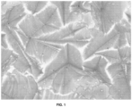
- Fig. 1 shows an optical microphotograph of an example of a transparent conductive metal layer comprised of interconnected crystalline metal dendritic "flakes" according to an embodiment of the present disclosure.
- Fig. 6 is an example of a single dendritic "flake.”
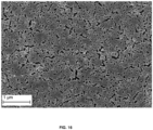
- the flakes cannot be easily distinguished, and the resulting framework looks like a randomized interconnected network of metal nanocrystals as shown in Figs. 15 and 16 .
- the transparent conductive framework of the TCMI that is formed from the crystal growth ink consists of large (10-300 ⁇ m) crystalline metal dendritic "flakes".
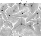
- a crystal node Figs. 2 , 7 .
- these "flakes” have polygonal shape. These "flakes” can be tiled or adjoined edge-to-edge, or they can overlap.
- the "flakes” can be both convex and concave.
- An example of the arrangement of such "flakes” i.e. of such conductive framework
- Fig. 6 An example of a single "flake” is shown on Fig. 6 .
- the "flakes” have a dendritic, multi-branching, snowflake-like shape.
- several thicker branches split from the center and spread over the area of the "flake” (see Figs. 3 and 8 ). Herein they are called “main branches”.
- the main branches branch out by themselves, creating a tree-like dendritic structure.
- the thinner branches that start not from the nodes or other branches are called “secondary branches”.
- the secondary branches can be straight or curved ( Fig. 9 ).
- the growth pattern, length and thickness of the main and secondary branches define the shape of the "flake", its borders ( Figs. 4 , 10 ) and its intersections with other flakes ( Figs. 5 , 11 ).
- the connection points between the "flakes” contribute to the whole framework's conductivity.
- the voids between the secondary branches of the "flakes” and the void between the "flakes” themselves contribute to the whole structure's transparency.
- Figs. 2 through 5 show different elements of the conductive framework.
- Stars 10 shown in Fig. 2 represent crystal nodes inside the "flakes”.
- Dashed lines 14 shown in Fig. 3 represent main branches inside the "flakes”.
- Dashed lines 18 on Fig. 4 represent approximate borders of the "flakes”.
- "X" signs 22 on Fig. 5 marks connection points between the "flakes”.
- Figs. 7 through 11 show different elements of a single "flake".
- a star 24 on Fig. 7 represents crystal node inside the "flake”.
- Long dashed lines 26 on Fig. 8 represent main branches inside the "flakes”.
- Dotted lines 28 on Fig. 9 represent some of the secondary branches inside the "flake”.
- Short dashed lines 30 on Fig. 10 represent approximate borders of the "flake”.
- "X" signs 32 on Fig. 11 mark connection points between the central "flake” and the adjacent "flakes”.
- Several "flakes” with thicker main branches are shown on an electron micrograph picture on Fig. 12 .
- Some examples of the tree-like dendritic nature of the main and secondary branches are shown on Figs. 13 and 14 .
- the "flakes" cannot be identified from the SEM imaging, but the TCML retains its conductivity and transparency properties.
- An example of such a structure can be found in Figs. 15 and 16 . lt can be clearly seen, that this is also as interconnected dendritic structure, not dissimilar to the ones shown above.
- the larger scale flake features for example, "main branches”
- the smaller scale features for example, "secondary branches”
- the crystal growth ink composition includes a metal ionic precursor, comprising between 0.01% and 20% by weight of the crystal growth ink.
- the composition of the crystal growth ink may be in the form of a solution, a dispersion, a suspension, a gel, or a colloid.
- the metal ionic precursor of the crystal growth ink may be composed of a mixture of salts including one or more metal cations (i.e., positively charged ions) and counterions (i.e., ions having a charge equal to the cations, but negative).
- the metal cations may be stabilized by either a counterion or a ligand, forming an organometallic complex, such that the resulting salt is connected by coordinate bonds rather than by ionic bonds.
- the metal cations may be in the form of an organic or inorganic salt of at least one of the following elements: Au, Ag, Pt, Pd, Cu, Ni, Co, Zn, In, Ti, V, Mn, Fe, Cr, Zr, Nb, Mo, W, Ru, Rh, Ca, Re, Os, Ir, Al, Ga, Sn, and Sb, and their combinations.
- Their salts may form metallic or bimetallic nanocrystals.
- it may be preferential that the metal cations may be an organic or an inorganic salt of silver (Ag).
- the counterions of the metal ionic precursor may be M(NO3)n, M(SO4)n, MCIn, HmMCIn+m, and MN, where "M” is a metal atom, or metal alloy, with a valence of "n", H is hydrogen, NO3 is nitrate, SO4 is sulfate, Cl is chloride, "N” is alkyl-, alyl-, aceto-, carbonyl, carboxyl, cyclopentadienyl, phenyl-, biphenyl-, pyridine-, bipyridine-, aromatic, cyano-, amide and other organic moieties, and "m” is a valence of the counterion.
- the crystal growth ink composition includes 80% to 99.99% by weight of the liquid part of the ink that includes a combination of chemical solvents whose purpose is, first, to help spreading and/or printing of the crystal growth ink on the surface, and, second, ensure the proper crystal growth parameters, including but not limited to crystal size, crystal shape, layer roughness, layer flexibility, layer transparency and layer conductivity.
- the liquid part of the ink consists of two parts, a structuring liquid, and a spreading liquid. Both of the parts can be one or a combination of several organic solvents.
- the structuring liquid has a high dynamic viscosity parameter.
- the structuring liquid has a dynamic viscosity between 20-100 mPa ⁇ s (20-100 centipoise (cP))
- the spreading liquid has a low surface tension parameter.
- the structuring liquid may include any one or combination of cyclic alcohols, sulfoxides, formamides, ethylamines, diols, glycols, glycol ethers, glycerol, propylene carbonate, and their derivatives.
- the spreading liquid has a surface tension of 10-40 millinewtons per meter (mN/m). In some embodiments it is preferential if the spreading liquid is at least one of: alcohol, toluene, dioxane, sulfoxides, formamides, ethylamines, glycol ethers, acetonitrile and their derivatives.
- the liquid part of the ink only evaporates during plasma exposure under the combined effect of plasma irradiation and atmospheric pressure to medium vacuum (1 ⁇ 10 5 Pa to 1 ⁇ 10 -1 Pa).
- the disclosed method includes applying the crystal growth ink to a substrate by various means including, but not limited to, drop-casting, spray-coating, immersion, inkjet printing, aerosol spraying, slot-die casting, spin-coating and screen printing.
- the thickness of the crystal growth ink on the substrate should not exceed 2 millimeters.
- the coated substrate is then exposed to irradiation from plasma.
- the plasma used for the irradiation includes plasma having partially ionized gas that is not in thermodynamic equilibrium, such as radio frequency (RF) plasma. Often, such plasma can exist at relatively low temperatures. Such plasma can be in both low to medium and atmospheric pressure.
- RF radio frequency
- the plasma may include a gas such as Argon, Nitrogen, Oxygen, Hydrogen, air, Helium, Neon, Xenon, Ammonia, Ethane (C2H6), Carbon dioxide, Carbon monoxide, Methane (CH4), Propane (C3H8), Silane (SiH4), Nitrogen dioxide, Nitrogen monoxide and their combinations.
- the plasma gas is an inert gas.
- the plasma gas is Argon, Nitrogen, Neon or Xenon.
- the substrate is exposed to gas plasma as determined by a set of exposure parameters including, but not limited to, power, RF frequency, and time duration of the exposure. The values of the exposure parameters are determined, based in part, on the type of the substrate, the composition of the crystal growth ink, and the means of the application of the crystal growth ink.
- the values of the exposure parameters fall within the following ranges: the power is up to 3000 Watts (W), the plasma RF frequency is between 50Hz and 5GHz, and the exposure time is between 1 and 3600 seconds. In an embodiment not belonging to the present invention it is preferential if the plasma power is 50-200 W, the plasma RF frequency is between 30 kHz and 20 MHz, and the exposure time is between 5 and 600 seconds. In an embodiment, the plasma frequency is 40 kHz. In another embodiment, the plasma frequency is 13.56 MHz.
- the metal ionic precursor therein reacts with the plasma, resulting in its electrochemical reduction.
- the majority (at least 95%) of the liquid part of the ink evaporates, and metal ions receive electrons from the plasma and are converted into metal atoms. These processes occur simultaneously.
- the metal atoms assemble into a nanocrystalline framework that adheres to the substrate. The density and therefore transparency and conductivity of the framework can be controlled.
- the transparency of the resulting metal films is between 30% and 95% in the wavelength range of about 370 nm to 770 nm.
- the conductivity of the metal films is between 0.01 ohm/square to 500 ohm/square.
- the resulting metal films are highly flexible when grown on a flexible substrate, and do not exhibit fatal cracking after 1000 bending cycles.
- the crystal growth ink includes the metal ionic precursor AgNO3 with a concentration of 5 wt. % of the crystal growth ink.
- the ink is loaded into an Epson printhead.
- a PET substrate is activated using plasma irradiation for 10 seconds.
- the substrate is loaded into the printer and a rectangular shape is printed using the crystal growth ink.
- the PET is then put into a plasma chamber and the chamber is set with the following exposure parameters for power, gas flow rate, and time: RF frequency of 13.56 MHz, 150 W of power, 30 SCCM gas flow rate, and 5 minutes of exposure, respectively.
- the result is a conductive transparent print.
- the print resistivity is 4 ohm/sq.
- the film transparency is 50%.
- Fig. 2 shows an optical microscope image of similarly prepared transparent conductive film.
- the crystal growth ink includes the metal ionic precursor AgNO3 with a concentration of 1 wt. % of the crystal growth ink.
- the ink is loaded into a Konica Minolta printhead.
- An AS-sized PET substrate is activated using plasma irradiation for 1 minute.
- the substrate is loaded into the printer and the whole substrate is printed on with the crystal growth ink.
- the PET is then put into a plasma chamber and the chamber is set with the following exposure parameters for power, gas flow rate, and time: RF frequency of 13.56 MHz, 150 W of power, 20 SCCM gas flow rate, and 5 minutes of exposure, respectively.
- the result is a conductive transparent print.
- the print resistivity is 130 ohm/sq.
- the film transparency is 70%.
- Fig. 4 shows an electron microscope image of similarly prepared transparent conductive film.
- the crystal growth ink includes the metal ionic precursor AgNO3 with a concentration of 2.5 wt. % of the crystal growth ink.
- the ink is loaded into a Dimatix printhead.
- a PET substrate is cleaned using a piranha solution and dried thoroughly.
- a rectangular shape is printed with a flatbed printer using the crystal growth ink.
- the PET is then put into a plasma chamber and the chamber is set with the following exposure parameters for power, gas flow rate, and time: RF frequency of 13.56 MHz, 150 W of power, 30 SCCM gas flow rate, and 5 minutes of exposure, respectively.
- the result is a conductive transparent print on glass.
- the print resistivity is 15 ohm/sq.
- the film transparency is 80%.
- the crystal growth ink includes the metal ionic precursor AgNO3 with a concentration of 6 wt. % of the crystal growth ink.
- the ink is loaded into a Konica printhead.
- a PET substrate is activated using plasma irradiation for 20 seconds.
- the substrate is loaded into the printer and a rectangular shape is printed using the crystal growth ink.
- the PET is then put into a plasma chamber and the chamber is set with the following exposure parameters for power, gas flow rate, and time: RF frequency of 13.56 MHz, 150 W of power, 30 SCCM gas flow rate, and 2 minutes of exposure, respectively.
- the result is a conductive transparent print.
- the print resistivity is 4 ohm/sq.
- the film transparency is 35%.
- the crystal growth ink includes the metal ionic precursor AgNO3 with a concentration of 10 wt. % of the crystal growth ink.
- the ink is loaded into a Spectra printhead.
- a PET substrate is activated using plasma irradiation for 30 seconds.
- the substrate is loaded into the printer and a rectangular shape is printed using the crystal growth ink.
- the PET is then put into a plasma chamber and the chamber is set with the following exposure parameters for power, gas flow rate, and time: RF frequency of 13.56 MHz, 150 W of power, 30 SCCM gas flow rate, and 5 minutes of exposure, respectively.
- the result is a conductive transparent print.
- the print resistivity is 30 ohm/sq.
- the film transparency is 60%.
- the crystal growth ink includes the metal ionic precursor AgNO3 with a concentration of 0.5 wt. % of the crystal growth ink.
- a PET substrate is activated using plasma irradiation for 10 seconds.
- the ink is spread on the PET substrate using an aerosol jet.
- the PET is then put into a plasma chamber and the chamber is set with the following exposure parameters for power, gas flow rate, and time: RF frequency of 13.56 MHz, 150 W of power, 30 SCCM gas flow rate, and 10 minutes of exposure, respectively.
- the result is a conductive transparent print.
- the print resistivity is 20 ohm/sq.
- the film transparency is 40%.
- the crystal growth ink includes the metal ionic precursor silver nitrate with a concentration of 3.5 wt. % of the crystal growth ink.
- the ink is loaded into a Spectra printhead.
- the PET substrate is loaded into the printer and a rectangular shape is printed using the crystal growth ink.
- the PET is then put into a plasma chamber and the chamber is set with the following exposure parameters for power, gas flow rate, and time: RF frequency of 40 kHz, 150 W of power, 30 SCCM gas flow rate, and 5 minutes of exposure, respectively.
- the result is a conductive transparent print.
- the print resistivity is 15 ohm/sq.
- the film transparency is 80%.
- Fig. 15 shows an SEM image of similarly prepared transparent conductive film.
- the crystal growth ink includes the metal ionic precursor silver acetate with a concentration of 13 wt. % of the crystal growth ink.
- the ink is loaded into a Spectra printhead.
- An AS-sized PET substrate is activated using plasma irradiation for 1 minute.
- the PET substrate is loaded into the printer and a rectangular shape is printed using the crystal growth ink.
- the PET is then put into a plasma chamber and the chamber is set with the following exposure parameters for power, gas flow rate, and time: RF frequency of 13.56 MHz, 200 W of power, 20 SCCM gas flow rate, and 10 minutes of exposure, respectively.
- the result is a conductive transparent print.
- the print resistivity is 130 ohm/sq.
- the film transparency is 70%.
- Example IX (comparative).
- the crystal growth ink includes the metal ionic precursor AuCI4H2 with a concentration of 2.5 wt. % of the crystal growth ink.
- the ink is loaded into a Konica acid resistant printhead.
- a PET substrate is cleaned using a piranha solution and dried thoroughly.
- a rectangular shape is printed with a flatbed printer using the crystal growth ink.
- the PET is then put into a plasma chamber and the chamber is set with the following exposure parameters for power, gas flow rate, and time: RF frequency of 13.56 MHz, 150 W of power, 30 SCCM gas flow rate, and 10 minutes of exposure, respectively.
- the result is a conductive transparent print on glass.
- the print resistivity is 15 ohm/sq.
- the film transparency is 80%.
- the crystal growth ink includes the metal ionic precursor AgNO3 with a concentration of 6 wt. % of the crystal growth ink.
- the liquid part of the ink consists of a combination of ethylene glycol and propylene glycol as a structuring liquid, and a combination of Dowanol PM and propyl cellosolve as a spreading liquid.
- the ink is loaded into a Spectra printhead.
- the PET substrate is loaded into the printer and a rectangular shape is printed using the crystal growth ink.
- the PET is then put into a plasma chamber and the chamber is set with the following exposure parameters for power, gas flow rate, and time: RF frequency of 40 kHz, 200 W of power, 25 SCCM gas flow rate, and 5 minutes of exposure, respectively.
- the result is a conductive transparent print.
- the print resistivity is 70 ohm/sq.
- the film transparency is 85%.
- Example XI (comparative).
- the crystal growth ink includes the metal ionic precursor silver sulphate with a concentration of 1 wt. % of the crystal growth ink.
- the ink is spread on a substrate using a slot-die coater.
- the substrate is then put into a plasma chamber and the chamber is set with the following exposure parameters for power, gas flow rate, and time: RF frequency of 13.56 MHz, 150 W of power, 30 SCCM gas flow rate, and 3 minutes of exposure, respectively.
- the result is a conductive transparent print.
- the print resistivity is 30 ohm/sq.
- the film transparency is 60%.
- Example XII (comparative).
- the crystal growth ink includes the metal ionic precursor silver acetate with a concentration of 3 wt. % of the crystal growth ink.
- a PET substrate is activated using plasma irradiation for 10 seconds.
- the ink is spread on the PET substrate using a slot-die coater.
- the PET is then put into a plasma chamber and the chamber is set with the following exposure parameters for power, gas flow rate, and time: RF frequency of 40 kHz MHz, 150 W of power, 30 SCCM gas flow rate, and 10 minutes of exposure, respectively.
- the result is a conductive transparent print.
- the print resistivity is 20 ohm/sq.
- the film transparency is 40%.
- the phrase "at least one of” followed by a listing of items means that any of the listed items can be utilized individually, or any combination of two or more of the listed items can be utilized. For example, if a system is described as including "at least one of A, B, and C," the system can include A alone; B alone; C alone; A and B in combination; B and C in combination; A and C in combination; or A, B, and C in combination.
Landscapes
- Chemical & Material Sciences (AREA)
- Engineering & Computer Science (AREA)
- Organic Chemistry (AREA)
- Materials Engineering (AREA)
- Wood Science & Technology (AREA)
- Life Sciences & Earth Sciences (AREA)
- General Chemical & Material Sciences (AREA)
- Chemical Kinetics & Catalysis (AREA)
- Inorganic Chemistry (AREA)
- Physics & Mathematics (AREA)
- Metallurgy (AREA)
- Mechanical Engineering (AREA)
- Plasma & Fusion (AREA)
- Thermal Sciences (AREA)
- Health & Medical Sciences (AREA)
- Toxicology (AREA)
- Inks, Pencil-Leads, Or Crayons (AREA)
- Manufacturing Of Electric Cables (AREA)
- Non-Insulated Conductors (AREA)
Claims (13)
- Procédé de croissance d'une couche métallique conductrice transparente sur un substrat, comprenant :activer le substrat en utilisant une irradiation plasma pendant une durée prédéterminée ;appliquer une encre de croissance cristalline sur une surface du substrat, l'encre de croissance cristalline comprenant un précurseur ionique métallique ;exposer le substrat à l'irradiation plasma pour entraîner la croissance de la couche métallique conductrice transparente composée d'une structure métallique cristalline sur le substrat, dans lequel l'exposition est basée sur un ensemble de paramètres d'exposition prédéfinis ;dans lequel le substrat est un substrat PET ;dans lequel l'encre de croissance cristalline comprend un composant liquide de structuration et un composant liquide d'étalement, tous deux étant un solvant organique ouune combinaison de solvants organiques ; et dans lequel soit :i) l'ensemble de paramètres d'exposition prédéfinis comprend une fréquence RF de 13,56 MHz, une puissance de 150 W et un débit de gaz de 30 SCCM, dans lequel le précurseur ionique métallique est le nitrate d'argent avec une concentration de 5 % en poids de l'encre de croissance cristalline, dans lequel la couche métallique conductrice formée a une résistivité de 4 ohm/sq / ohm/carré et une transparence de 50 %, et dans lequel la structure métallique cristalline comprend de larges flocons dendritiques métalliques cristallins ayant chacun un noeud cristallin en leur centre ;
soitii) l'ensemble de paramètres d'exposition prédéfinis comprend une fréquence RF de 40 kHz, une puissance de 150 W et un débit de gaz de 30 SCCM; dans lequel le précurseur ionique métallique est le nitrate d'argent à une concentration de 3,5 % en poids de l'encre de croissance cristalline; dans lequel la couche métallique conductrice formée a une résistivité de 15 ohm/sq / ohm/carré et une transparence de 80 % ; et dans lequel la structure métallique cristalline comprend un réseau interconnecté aléatoire de nanocristaux métalliques. - Procédé selon la revendication 1, dans lequel l'encre de croissance cristalline comprend le précurseur ionique métallique à une concentration comprise entre 0,01% et 20% en poids de l'encre de croissance cristalline, et dans lequel l'encre de croissance cristalline est une parmi une solution, une dispersion, une suspension, un gel ou un colloïde.
- Procédé selon la revendication 1, dans lequel le précurseur ionique métallique comprend un mélange de sels incluant un ou plusieurs cations métalliques et contre-ions.
- Procédé selon la revendication 3, dans lequel les cations métalliques sont stabilisés par un parmi un contre-ion ou un ligand, dans lequel les cations métalliques stabilisés forment un complexe organométallique, de sorte que le sel résultant est lié par liaisons de coordination plutôt que par liaisons ioniques.
- Procédé selon la revendication 3, dans lequel les cations métalliques sont un sel organique ou un sel inorganique d'Ag.
- Procédé selon la revendication 3, dans lequel les cations métalliques sont un sel organique ou un sel inorganique parmi au moins un des éléments suivants : Au, Pt, Pd, Cu, Ni, Co, Zn, In, Ti, V, Mn, Fe, Cr, Zr, Nb, Mo, W, Ru, Rh, Ca, Re, Os, Ir, Al, Ga, Sn, Sb, et leur combinaison.
- Procédé selon la revendication 3, dans lequel les contre-ions du précurseur ionique métallique sont choisis dans le groupe constitué de : M(NO3)n, M(SO4)n, MCln, HmMCln+m, et MN, où "M" est un atome de métal, ou un alliage métallique, avec une valence de "n", H est l'hydrogène, NO3 est un nitrate, SO4 est un sulfate, Cl est un chlorure, "N" est un alkyl-, un alyl-, un acéto-, un carbonyle, un carboxyle, un cyclopentadiényle, un phényle, un biphényle, une pyridine, une bipyridine, un aromatique, un cyano, une amide et autres groupements organiques, et "m" une valence du contre-ion.
- Procédé selon la revendication 1, dans lequel l'encre de croissance cristalline comprend un ou plusieurs solvants à une concentration comprise entre 80 % et 99,99 % en poids de la partie liquide de l'encre.
- Procédé selon la revendication 1, dans lequel le composant liquide de structuration a un paramètre de viscosité dynamique compris entre 20 et 100 mPa.s (20 et 100 centipoises (cP)).
- Procédé selon la revendication 1, dans lequel le composant liquide de structuration comprend un ou une combinaison parmi: alcools cycliques, sulfoxydes, formamides, éthylamines, diols, glycols, éthers de glycol, glycérol, carbonate de propylène, et leurs dérivés.
- Procédé selon la revendication 1, dans lequel le composant liquide d'étalement a une tension superficielle entre 10 et 40 millinewtons par mètre (mN/m).
- Procédé selon la revendication 1, dans lequel l'ensemble de paramètres d'exposition prédéfinis comprend en outre une exposition au plasma à une pression allant de la pression atmosphérique de 1×10^5 Pa au vide moyen de 1×10^-1 Pa.
- Film métallique conducteur transparent mis à croître sur un substrat en utilisant le procédé de la revendication 1 avec i) ou ii).
Applications Claiming Priority (2)
| Application Number | Priority Date | Filing Date | Title |
|---|---|---|---|
| US201862776627P | 2018-12-07 | 2018-12-07 | |
| PCT/IB2019/060441 WO2020115680A1 (fr) | 2018-12-07 | 2019-12-04 | Couches métalliques conductrices transparentes |
Publications (3)
| Publication Number | Publication Date |
|---|---|
| EP3887463A1 EP3887463A1 (fr) | 2021-10-06 |
| EP3887463A4 EP3887463A4 (fr) | 2022-01-26 |
| EP3887463B1 true EP3887463B1 (fr) | 2023-09-13 |
Family
ID=70974650
Family Applications (1)
| Application Number | Title | Priority Date | Filing Date |
|---|---|---|---|
| EP19892623.0A Active EP3887463B1 (fr) | 2018-12-07 | 2019-12-04 | Couches métalliques conductrices transparentes |
Country Status (4)
| Country | Link |
|---|---|
| US (1) | US20210309868A1 (fr) |
| EP (1) | EP3887463B1 (fr) |
| CN (1) | CN113383046A (fr) |
| WO (1) | WO2020115680A1 (fr) |
Cited By (1)
| Publication number | Priority date | Publication date | Assignee | Title |
|---|---|---|---|---|
| WO2025176763A1 (fr) | 2024-02-21 | 2025-08-28 | OrelTech GmbH | Procédé de formation d'un revêtement métallique à partir d'un liquide de métallisation |
Family Cites Families (9)
| Publication number | Priority date | Publication date | Assignee | Title |
|---|---|---|---|---|
| US7258899B1 (en) | 2001-12-13 | 2007-08-21 | Amt Holdings, Inc. | Process for preparing metal coatings from liquid solutions utilizing cold plasma |
| PL1853671T3 (pl) * | 2005-03-04 | 2014-01-31 | Inktec Co Ltd | Tusze przewodzące i sposób ich wytwarzania |
| JP2008108541A (ja) * | 2006-10-25 | 2008-05-08 | Sumitomo Osaka Cement Co Ltd | 透明導電膜の形成方法及び透明導電膜 |
| KR101904912B1 (ko) * | 2010-01-15 | 2018-10-08 | 씨에이엠 홀딩 코포레이션 | 저헤이즈 투명 도전체 |
| CN113930707B (zh) * | 2014-10-21 | 2024-04-16 | 奥雷尔科技有限公司 | 一种在基底上形成图案化金属膜的方法和系统 |
| US9763325B2 (en) * | 2015-04-07 | 2017-09-12 | Oregon State University | Microreactor-assisted printing of conductive traces with in-situ reactive inks |
| WO2018049322A1 (fr) * | 2016-09-12 | 2018-03-15 | Oreltech Ltd. | Formation de composant actif métallique dans des matériaux hybrides |
| EP3574128A4 (fr) * | 2017-01-24 | 2020-12-23 | Oreltech Ltd. | Procédé de formation de couche métallique |
| US11230132B2 (en) * | 2017-04-13 | 2022-01-25 | Case Western Reserve University | Composition comprising directly written metal features and method of formation |
-
2019
- 2019-12-04 EP EP19892623.0A patent/EP3887463B1/fr active Active
- 2019-12-04 WO PCT/IB2019/060441 patent/WO2020115680A1/fr not_active Ceased
- 2019-12-04 CN CN201980090638.XA patent/CN113383046A/zh active Pending
-
2021
- 2021-06-07 US US17/340,719 patent/US20210309868A1/en active Pending
Cited By (1)
| Publication number | Priority date | Publication date | Assignee | Title |
|---|---|---|---|---|
| WO2025176763A1 (fr) | 2024-02-21 | 2025-08-28 | OrelTech GmbH | Procédé de formation d'un revêtement métallique à partir d'un liquide de métallisation |
Also Published As
| Publication number | Publication date |
|---|---|
| CN113383046A (zh) | 2021-09-10 |
| EP3887463A4 (fr) | 2022-01-26 |
| EP3887463A1 (fr) | 2021-10-06 |
| US20210309868A1 (en) | 2021-10-07 |
| WO2020115680A1 (fr) | 2020-06-11 |
Similar Documents
| Publication | Publication Date | Title |
|---|---|---|
| US9972742B2 (en) | Method for forming a transparent conductive film with metal nanowires having high linearity | |
| TWI525033B (zh) | 以奈米線為主之透明導體及其圖案化方法 | |
| JP4648504B2 (ja) | 金属酸化膜の形成方法および金属酸化膜 | |
| EP3209734B1 (fr) | Composition pour la formation d'un film métallique à motifs sur un substrat | |
| US20140205763A1 (en) | Growth of graphene films and graphene patterns | |
| US20080241391A1 (en) | Method of manufacturing a metal nanoparticle, conductive ink composition having the metal nanoparticle and method of forming a conductive pattern using the same | |
| US11746421B2 (en) | Method for metal layer formation | |
| JP2009094033A (ja) | 透明導電材料その製造方法及びそれを用いた透明導電素子 | |
| EP3887463B1 (fr) | Couches métalliques conductrices transparentes | |
| CN105659413A (zh) | 用于生产薄膜的湿式方法 | |
| Masuda et al. | Site-selective deposition of In2O3 using a self-assembled monolayer | |
| WO2025176763A1 (fr) | Procédé de formation d'un revêtement métallique à partir d'un liquide de métallisation | |
| US9159865B2 (en) | Method of forming zinc oxide prominence and depression structure and method of manufacturing solar cell using thereof | |
| CN110491599B (zh) | 一种复合导电薄膜的制备方法 | |
| KR100613405B1 (ko) | 전기장 결합형 플라즈마 화학 증착법에 의한 투명한 도전성 금속 복합박막의 제조방법 | |
| Curtis et al. | Direct-write printing of silver metallizations on silicon solar cells | |
| JP2006236747A (ja) | 透明電極及び透明電極の製造方法 | |
| JP2007294220A (ja) | 透明導電膜を有する基材 | |
| JP5157096B2 (ja) | 透明導電膜形成方法及び透明導電膜 | |
| JP2008108541A (ja) | 透明導電膜の形成方法及び透明導電膜 | |
| WO2018201952A1 (fr) | Procédé de production de graphène et dispositif pour sa réalisation | |
| KR100686318B1 (ko) | 전도성 탄소계 나노구조 코팅장치 및 방법 | |
| Akasaka et al. | Structured MgO coated electrodes to reduce the inception voltage | |
| JP2007234442A (ja) | 電界放出素子とその製造方法 | |
| KR20160080846A (ko) | 전계방출원의 제조방법 및 그에 따라 제조된 전계방출원 |
Legal Events
| Date | Code | Title | Description |
|---|---|---|---|
| STAA | Information on the status of an ep patent application or granted ep patent |
Free format text: STATUS: THE INTERNATIONAL PUBLICATION HAS BEEN MADE |
|
| PUAI | Public reference made under article 153(3) epc to a published international application that has entered the european phase |
Free format text: ORIGINAL CODE: 0009012 |
|
| STAA | Information on the status of an ep patent application or granted ep patent |
Free format text: STATUS: REQUEST FOR EXAMINATION WAS MADE |
|
| 17P | Request for examination filed |
Effective date: 20210701 |
|
| AK | Designated contracting states |
Kind code of ref document: A1 Designated state(s): AL AT BE BG CH CY CZ DE DK EE ES FI FR GB GR HR HU IE IS IT LI LT LU LV MC MK MT NL NO PL PT RO RS SE SI SK SM TR |
|
| STAA | Information on the status of an ep patent application or granted ep patent |
Free format text: STATUS: EXAMINATION IS IN PROGRESS |
|
| A4 | Supplementary search report drawn up and despatched |
Effective date: 20220104 |
|
| RIC1 | Information provided on ipc code assigned before grant |
Ipc: C09D 11/101 20140101ALI20211221BHEP Ipc: C09D 5/24 20060101ALI20211221BHEP Ipc: C30B 7/06 20060101ALI20211221BHEP Ipc: C23C 18/14 20060101ALI20211221BHEP Ipc: C23C 18/31 20060101ALI20211221BHEP Ipc: C09D 11/52 20140101AFI20211221BHEP |
|
| 17Q | First examination report despatched |
Effective date: 20220114 |
|
| DAV | Request for validation of the european patent (deleted) | ||
| DAX | Request for extension of the european patent (deleted) | ||
| RIC1 | Information provided on ipc code assigned before grant |
Ipc: C23C 18/08 20060101ALI20230404BHEP Ipc: C09D 11/36 20140101ALI20230404BHEP Ipc: C09D 11/322 20140101ALI20230404BHEP Ipc: C09D 11/037 20140101ALI20230404BHEP Ipc: C09D 11/033 20140101ALI20230404BHEP Ipc: C09D 1/00 20060101ALI20230404BHEP Ipc: C09D 11/101 20140101ALI20230404BHEP Ipc: C09D 5/24 20060101ALI20230404BHEP Ipc: C30B 7/06 20060101ALI20230404BHEP Ipc: C23C 18/14 20060101ALI20230404BHEP Ipc: C23C 18/31 20060101ALI20230404BHEP Ipc: C09D 11/52 20140101AFI20230404BHEP |
|
| GRAP | Despatch of communication of intention to grant a patent |
Free format text: ORIGINAL CODE: EPIDOSNIGR1 |
|
| STAA | Information on the status of an ep patent application or granted ep patent |
Free format text: STATUS: GRANT OF PATENT IS INTENDED |
|
| INTG | Intention to grant announced |
Effective date: 20230512 |
|
| GRAS | Grant fee paid |
Free format text: ORIGINAL CODE: EPIDOSNIGR3 |
|
| GRAA | (expected) grant |
Free format text: ORIGINAL CODE: 0009210 |
|
| STAA | Information on the status of an ep patent application or granted ep patent |
Free format text: STATUS: THE PATENT HAS BEEN GRANTED |
|
| AK | Designated contracting states |
Kind code of ref document: B1 Designated state(s): AL AT BE BG CH CY CZ DE DK EE ES FI FR GB GR HR HU IE IS IT LI LT LU LV MC MK MT NL NO PL PT RO RS SE SI SK SM TR |
|
| REG | Reference to a national code |
Ref country code: CH Ref legal event code: EP |
|
| REG | Reference to a national code |
Ref country code: DE Ref legal event code: R096 Ref document number: 602019037630 Country of ref document: DE |
|
| REG | Reference to a national code |
Ref country code: IE Ref legal event code: FG4D |
|
| P01 | Opt-out of the competence of the unified patent court (upc) registered |
Effective date: 20230915 |
|
| REG | Reference to a national code |
Ref country code: LT Ref legal event code: MG9D |
|
| REG | Reference to a national code |
Ref country code: NL Ref legal event code: MP Effective date: 20230913 |
|
| PG25 | Lapsed in a contracting state [announced via postgrant information from national office to epo] |
Ref country code: GR Free format text: LAPSE BECAUSE OF FAILURE TO SUBMIT A TRANSLATION OF THE DESCRIPTION OR TO PAY THE FEE WITHIN THE PRESCRIBED TIME-LIMIT Effective date: 20231214 |
|
| PG25 | Lapsed in a contracting state [announced via postgrant information from national office to epo] |
Ref country code: SE Free format text: LAPSE BECAUSE OF FAILURE TO SUBMIT A TRANSLATION OF THE DESCRIPTION OR TO PAY THE FEE WITHIN THE PRESCRIBED TIME-LIMIT Effective date: 20230913 Ref country code: RS Free format text: LAPSE BECAUSE OF FAILURE TO SUBMIT A TRANSLATION OF THE DESCRIPTION OR TO PAY THE FEE WITHIN THE PRESCRIBED TIME-LIMIT Effective date: 20230913 Ref country code: NO Free format text: LAPSE BECAUSE OF FAILURE TO SUBMIT A TRANSLATION OF THE DESCRIPTION OR TO PAY THE FEE WITHIN THE PRESCRIBED TIME-LIMIT Effective date: 20231213 Ref country code: LV Free format text: LAPSE BECAUSE OF FAILURE TO SUBMIT A TRANSLATION OF THE DESCRIPTION OR TO PAY THE FEE WITHIN THE PRESCRIBED TIME-LIMIT Effective date: 20230913 Ref country code: LT Free format text: LAPSE BECAUSE OF FAILURE TO SUBMIT A TRANSLATION OF THE DESCRIPTION OR TO PAY THE FEE WITHIN THE PRESCRIBED TIME-LIMIT Effective date: 20230913 Ref country code: HR Free format text: LAPSE BECAUSE OF FAILURE TO SUBMIT A TRANSLATION OF THE DESCRIPTION OR TO PAY THE FEE WITHIN THE PRESCRIBED TIME-LIMIT Effective date: 20230913 Ref country code: GR Free format text: LAPSE BECAUSE OF FAILURE TO SUBMIT A TRANSLATION OF THE DESCRIPTION OR TO PAY THE FEE WITHIN THE PRESCRIBED TIME-LIMIT Effective date: 20231214 Ref country code: FI Free format text: LAPSE BECAUSE OF FAILURE TO SUBMIT A TRANSLATION OF THE DESCRIPTION OR TO PAY THE FEE WITHIN THE PRESCRIBED TIME-LIMIT Effective date: 20230913 |
|
| REG | Reference to a national code |
Ref country code: AT Ref legal event code: MK05 Ref document number: 1611300 Country of ref document: AT Kind code of ref document: T Effective date: 20230913 |
|
| PG25 | Lapsed in a contracting state [announced via postgrant information from national office to epo] |
Ref country code: NL Free format text: LAPSE BECAUSE OF FAILURE TO SUBMIT A TRANSLATION OF THE DESCRIPTION OR TO PAY THE FEE WITHIN THE PRESCRIBED TIME-LIMIT Effective date: 20230913 |
|
| PG25 | Lapsed in a contracting state [announced via postgrant information from national office to epo] |
Ref country code: IS Free format text: LAPSE BECAUSE OF FAILURE TO SUBMIT A TRANSLATION OF THE DESCRIPTION OR TO PAY THE FEE WITHIN THE PRESCRIBED TIME-LIMIT Effective date: 20240113 |
|
| PG25 | Lapsed in a contracting state [announced via postgrant information from national office to epo] |
Ref country code: AT Free format text: LAPSE BECAUSE OF FAILURE TO SUBMIT A TRANSLATION OF THE DESCRIPTION OR TO PAY THE FEE WITHIN THE PRESCRIBED TIME-LIMIT Effective date: 20230913 |
|
| PG25 | Lapsed in a contracting state [announced via postgrant information from national office to epo] |
Ref country code: ES Free format text: LAPSE BECAUSE OF FAILURE TO SUBMIT A TRANSLATION OF THE DESCRIPTION OR TO PAY THE FEE WITHIN THE PRESCRIBED TIME-LIMIT Effective date: 20230913 |
|
| PG25 | Lapsed in a contracting state [announced via postgrant information from national office to epo] |
Ref country code: SM Free format text: LAPSE BECAUSE OF FAILURE TO SUBMIT A TRANSLATION OF THE DESCRIPTION OR TO PAY THE FEE WITHIN THE PRESCRIBED TIME-LIMIT Effective date: 20230913 Ref country code: RO Free format text: LAPSE BECAUSE OF FAILURE TO SUBMIT A TRANSLATION OF THE DESCRIPTION OR TO PAY THE FEE WITHIN THE PRESCRIBED TIME-LIMIT Effective date: 20230913 Ref country code: IS Free format text: LAPSE BECAUSE OF FAILURE TO SUBMIT A TRANSLATION OF THE DESCRIPTION OR TO PAY THE FEE WITHIN THE PRESCRIBED TIME-LIMIT Effective date: 20240113 Ref country code: ES Free format text: LAPSE BECAUSE OF FAILURE TO SUBMIT A TRANSLATION OF THE DESCRIPTION OR TO PAY THE FEE WITHIN THE PRESCRIBED TIME-LIMIT Effective date: 20230913 Ref country code: EE Free format text: LAPSE BECAUSE OF FAILURE TO SUBMIT A TRANSLATION OF THE DESCRIPTION OR TO PAY THE FEE WITHIN THE PRESCRIBED TIME-LIMIT Effective date: 20230913 Ref country code: CZ Free format text: LAPSE BECAUSE OF FAILURE TO SUBMIT A TRANSLATION OF THE DESCRIPTION OR TO PAY THE FEE WITHIN THE PRESCRIBED TIME-LIMIT Effective date: 20230913 Ref country code: AT Free format text: LAPSE BECAUSE OF FAILURE TO SUBMIT A TRANSLATION OF THE DESCRIPTION OR TO PAY THE FEE WITHIN THE PRESCRIBED TIME-LIMIT Effective date: 20230913 Ref country code: PT Free format text: LAPSE BECAUSE OF FAILURE TO SUBMIT A TRANSLATION OF THE DESCRIPTION OR TO PAY THE FEE WITHIN THE PRESCRIBED TIME-LIMIT Effective date: 20240115 Ref country code: SK Free format text: LAPSE BECAUSE OF FAILURE TO SUBMIT A TRANSLATION OF THE DESCRIPTION OR TO PAY THE FEE WITHIN THE PRESCRIBED TIME-LIMIT Effective date: 20230913 |
|
| PG25 | Lapsed in a contracting state [announced via postgrant information from national office to epo] |
Ref country code: PL Free format text: LAPSE BECAUSE OF FAILURE TO SUBMIT A TRANSLATION OF THE DESCRIPTION OR TO PAY THE FEE WITHIN THE PRESCRIBED TIME-LIMIT Effective date: 20230913 Ref country code: IT Free format text: LAPSE BECAUSE OF FAILURE TO SUBMIT A TRANSLATION OF THE DESCRIPTION OR TO PAY THE FEE WITHIN THE PRESCRIBED TIME-LIMIT Effective date: 20230913 |
|
| REG | Reference to a national code |
Ref country code: DE Ref legal event code: R097 Ref document number: 602019037630 Country of ref document: DE |
|
| PG25 | Lapsed in a contracting state [announced via postgrant information from national office to epo] |
Ref country code: DK Free format text: LAPSE BECAUSE OF FAILURE TO SUBMIT A TRANSLATION OF THE DESCRIPTION OR TO PAY THE FEE WITHIN THE PRESCRIBED TIME-LIMIT Effective date: 20230913 |
|
| PLBE | No opposition filed within time limit |
Free format text: ORIGINAL CODE: 0009261 |
|
| STAA | Information on the status of an ep patent application or granted ep patent |
Free format text: STATUS: NO OPPOSITION FILED WITHIN TIME LIMIT |
|
| PG25 | Lapsed in a contracting state [announced via postgrant information from national office to epo] |
Ref country code: DK Free format text: LAPSE BECAUSE OF FAILURE TO SUBMIT A TRANSLATION OF THE DESCRIPTION OR TO PAY THE FEE WITHIN THE PRESCRIBED TIME-LIMIT Effective date: 20230913 |
|
| 26N | No opposition filed |
Effective date: 20240614 |
|
| PG25 | Lapsed in a contracting state [announced via postgrant information from national office to epo] |
Ref country code: LU Free format text: LAPSE BECAUSE OF NON-PAYMENT OF DUE FEES Effective date: 20231204 |
|
| PG25 | Lapsed in a contracting state [announced via postgrant information from national office to epo] |
Ref country code: MC Free format text: LAPSE BECAUSE OF FAILURE TO SUBMIT A TRANSLATION OF THE DESCRIPTION OR TO PAY THE FEE WITHIN THE PRESCRIBED TIME-LIMIT Effective date: 20230913 |
|
| REG | Reference to a national code |
Ref country code: BE Ref legal event code: MM Effective date: 20231231 |
|
| PG25 | Lapsed in a contracting state [announced via postgrant information from national office to epo] |
Ref country code: MC Free format text: LAPSE BECAUSE OF FAILURE TO SUBMIT A TRANSLATION OF THE DESCRIPTION OR TO PAY THE FEE WITHIN THE PRESCRIBED TIME-LIMIT Effective date: 20230913 Ref country code: LU Free format text: LAPSE BECAUSE OF NON-PAYMENT OF DUE FEES Effective date: 20231204 |
|
| REG | Reference to a national code |
Ref country code: IE Ref legal event code: MM4A |
|
| PG25 | Lapsed in a contracting state [announced via postgrant information from national office to epo] |
Ref country code: IE Free format text: LAPSE BECAUSE OF NON-PAYMENT OF DUE FEES Effective date: 20231204 |
|
| PG25 | Lapsed in a contracting state [announced via postgrant information from national office to epo] |
Ref country code: BE Free format text: LAPSE BECAUSE OF NON-PAYMENT OF DUE FEES Effective date: 20231231 |
|
| PG25 | Lapsed in a contracting state [announced via postgrant information from national office to epo] |
Ref country code: SI Free format text: LAPSE BECAUSE OF FAILURE TO SUBMIT A TRANSLATION OF THE DESCRIPTION OR TO PAY THE FEE WITHIN THE PRESCRIBED TIME-LIMIT Effective date: 20230913 |
|
| PG25 | Lapsed in a contracting state [announced via postgrant information from national office to epo] |
Ref country code: SI Free format text: LAPSE BECAUSE OF FAILURE TO SUBMIT A TRANSLATION OF THE DESCRIPTION OR TO PAY THE FEE WITHIN THE PRESCRIBED TIME-LIMIT Effective date: 20230913 Ref country code: IE Free format text: LAPSE BECAUSE OF NON-PAYMENT OF DUE FEES Effective date: 20231204 Ref country code: BE Free format text: LAPSE BECAUSE OF NON-PAYMENT OF DUE FEES Effective date: 20231231 |
|
| PG25 | Lapsed in a contracting state [announced via postgrant information from national office to epo] |
Ref country code: BG Free format text: LAPSE BECAUSE OF FAILURE TO SUBMIT A TRANSLATION OF THE DESCRIPTION OR TO PAY THE FEE WITHIN THE PRESCRIBED TIME-LIMIT Effective date: 20230913 |
|
| PG25 | Lapsed in a contracting state [announced via postgrant information from national office to epo] |
Ref country code: BG Free format text: LAPSE BECAUSE OF FAILURE TO SUBMIT A TRANSLATION OF THE DESCRIPTION OR TO PAY THE FEE WITHIN THE PRESCRIBED TIME-LIMIT Effective date: 20230913 |
|
| PG25 | Lapsed in a contracting state [announced via postgrant information from national office to epo] |
Ref country code: CY Free format text: LAPSE BECAUSE OF FAILURE TO SUBMIT A TRANSLATION OF THE DESCRIPTION OR TO PAY THE FEE WITHIN THE PRESCRIBED TIME-LIMIT; INVALID AB INITIO Effective date: 20191204 |
|
| PG25 | Lapsed in a contracting state [announced via postgrant information from national office to epo] |
Ref country code: HU Free format text: LAPSE BECAUSE OF FAILURE TO SUBMIT A TRANSLATION OF THE DESCRIPTION OR TO PAY THE FEE WITHIN THE PRESCRIBED TIME-LIMIT; INVALID AB INITIO Effective date: 20191204 |
|
| PG25 | Lapsed in a contracting state [announced via postgrant information from national office to epo] |
Ref country code: TR Free format text: LAPSE BECAUSE OF FAILURE TO SUBMIT A TRANSLATION OF THE DESCRIPTION OR TO PAY THE FEE WITHIN THE PRESCRIBED TIME-LIMIT Effective date: 20230913 |
|
| REG | Reference to a national code |
Ref country code: CH Ref legal event code: U11 Free format text: ST27 STATUS EVENT CODE: U-0-0-U10-U11 (AS PROVIDED BY THE NATIONAL OFFICE) Effective date: 20260101 |
|
| PGFP | Annual fee paid to national office [announced via postgrant information from national office to epo] |
Ref country code: DE Payment date: 20251217 Year of fee payment: 7 |
|
| PGFP | Annual fee paid to national office [announced via postgrant information from national office to epo] |
Ref country code: GB Payment date: 20251211 Year of fee payment: 7 |
|
| PGFP | Annual fee paid to national office [announced via postgrant information from national office to epo] |
Ref country code: FR Payment date: 20251218 Year of fee payment: 7 |
|
| PGFP | Annual fee paid to national office [announced via postgrant information from national office to epo] |
Ref country code: CH Payment date: 20260101 Year of fee payment: 7 |