EP3889321B1 - Verfahren zur herstellung einer halbleitersubstratanordnung - Google Patents
Verfahren zur herstellung einer halbleitersubstratanordnung Download PDFInfo
- Publication number
- EP3889321B1 EP3889321B1 EP21151070.6A EP21151070A EP3889321B1 EP 3889321 B1 EP3889321 B1 EP 3889321B1 EP 21151070 A EP21151070 A EP 21151070A EP 3889321 B1 EP3889321 B1 EP 3889321B1
- Authority
- EP
- European Patent Office
- Prior art keywords
- mask
- semiconductor substrate
- layer
- electrically conductive
- metallization layer
- Prior art date
- Legal status (The legal status is an assumption and is not a legal conclusion. Google has not performed a legal analysis and makes no representation as to the accuracy of the status listed.)
- Active
Links
Images


Classifications
-
- C—CHEMISTRY; METALLURGY
- C23—COATING METALLIC MATERIAL; COATING MATERIAL WITH METALLIC MATERIAL; CHEMICAL SURFACE TREATMENT; DIFFUSION TREATMENT OF METALLIC MATERIAL; COATING BY VACUUM EVAPORATION, BY SPUTTERING, BY ION IMPLANTATION OR BY CHEMICAL VAPOUR DEPOSITION, IN GENERAL; INHIBITING CORROSION OF METALLIC MATERIAL OR INCRUSTATION IN GENERAL
- C23C—COATING METALLIC MATERIAL; COATING MATERIAL WITH METALLIC MATERIAL; SURFACE TREATMENT OF METALLIC MATERIAL BY DIFFUSION INTO THE SURFACE, BY CHEMICAL CONVERSION OR SUBSTITUTION; COATING BY VACUUM EVAPORATION, BY SPUTTERING, BY ION IMPLANTATION OR BY CHEMICAL VAPOUR DEPOSITION, IN GENERAL
- C23C30/00—Coating with metallic material characterised only by the composition of the metallic material, i.e. not characterised by the coating process
-
- H—ELECTRICITY
- H10—SEMICONDUCTOR DEVICES; ELECTRIC SOLID-STATE DEVICES NOT OTHERWISE PROVIDED FOR
- H10W—GENERIC PACKAGES, INTERCONNECTIONS, CONNECTORS OR OTHER CONSTRUCTIONAL DETAILS OF DEVICES COVERED BY CLASS H10
- H10W70/00—Package substrates; Interposers; Redistribution layers [RDL]
- H10W70/01—Manufacture or treatment
- H10W70/05—Manufacture or treatment of insulating or insulated package substrates, or of interposers, or of redistribution layers
-
- C—CHEMISTRY; METALLURGY
- C23—COATING METALLIC MATERIAL; COATING MATERIAL WITH METALLIC MATERIAL; CHEMICAL SURFACE TREATMENT; DIFFUSION TREATMENT OF METALLIC MATERIAL; COATING BY VACUUM EVAPORATION, BY SPUTTERING, BY ION IMPLANTATION OR BY CHEMICAL VAPOUR DEPOSITION, IN GENERAL; INHIBITING CORROSION OF METALLIC MATERIAL OR INCRUSTATION IN GENERAL
- C23C—COATING METALLIC MATERIAL; COATING MATERIAL WITH METALLIC MATERIAL; SURFACE TREATMENT OF METALLIC MATERIAL BY DIFFUSION INTO THE SURFACE, BY CHEMICAL CONVERSION OR SUBSTITUTION; COATING BY VACUUM EVAPORATION, BY SPUTTERING, BY ION IMPLANTATION OR BY CHEMICAL VAPOUR DEPOSITION, IN GENERAL
- C23C14/00—Coating by vacuum evaporation, by sputtering or by ion implantation of the coating forming material
- C23C14/04—Coating on selected surface areas, e.g. using masks
- C23C14/042—Coating on selected surface areas, e.g. using masks using masks
-
- H—ELECTRICITY
- H10—SEMICONDUCTOR DEVICES; ELECTRIC SOLID-STATE DEVICES NOT OTHERWISE PROVIDED FOR
- H10K—ORGANIC ELECTRIC SOLID-STATE DEVICES
- H10K71/00—Manufacture or treatment specially adapted for the organic devices covered by this subclass
- H10K71/30—Doping active layers, e.g. electron transporting layers
-
- H—ELECTRICITY
- H10—SEMICONDUCTOR DEVICES; ELECTRIC SOLID-STATE DEVICES NOT OTHERWISE PROVIDED FOR
- H10K—ORGANIC ELECTRIC SOLID-STATE DEVICES
- H10K71/00—Manufacture or treatment specially adapted for the organic devices covered by this subclass
- H10K71/621—Providing a shape to conductive layers, e.g. patterning or selective deposition
-
- H—ELECTRICITY
- H10—SEMICONDUCTOR DEVICES; ELECTRIC SOLID-STATE DEVICES NOT OTHERWISE PROVIDED FOR
- H10P—GENERIC PROCESSES OR APPARATUS FOR THE MANUFACTURE OR TREATMENT OF DEVICES COVERED BY CLASS H10
- H10P76/00—Manufacture or treatment of masks on semiconductor bodies, e.g. by lithography or photolithography
- H10P76/20—Manufacture or treatment of masks on semiconductor bodies, e.g. by lithography or photolithography of masks comprising organic materials
- H10P76/202—Manufacture or treatment of masks on semiconductor bodies, e.g. by lithography or photolithography of masks comprising organic materials for lift-off processes
-
- H—ELECTRICITY
- H10—SEMICONDUCTOR DEVICES; ELECTRIC SOLID-STATE DEVICES NOT OTHERWISE PROVIDED FOR
- H10P—GENERIC PROCESSES OR APPARATUS FOR THE MANUFACTURE OR TREATMENT OF DEVICES COVERED BY CLASS H10
- H10P76/00—Manufacture or treatment of masks on semiconductor bodies, e.g. by lithography or photolithography
- H10P76/40—Manufacture or treatment of masks on semiconductor bodies, e.g. by lithography or photolithography of masks comprising inorganic materials
- H10P76/408—Manufacture or treatment of masks on semiconductor bodies, e.g. by lithography or photolithography of masks comprising inorganic materials characterised by their sizes, orientations, dispositions, behaviours or shapes
-
- H—ELECTRICITY
- H10—SEMICONDUCTOR DEVICES; ELECTRIC SOLID-STATE DEVICES NOT OTHERWISE PROVIDED FOR
- H10W—GENERIC PACKAGES, INTERCONNECTIONS, CONNECTORS OR OTHER CONSTRUCTIONAL DETAILS OF DEVICES COVERED BY CLASS H10
- H10W40/00—Arrangements for thermal protection or thermal control
- H10W40/20—Arrangements for cooling
- H10W40/25—Arrangements for cooling characterised by their materials
- H10W40/255—Arrangements for cooling characterised by their materials having a laminate or multilayered structure, e.g. direct bond copper [DBC] ceramic substrates
-
- H—ELECTRICITY
- H10—SEMICONDUCTOR DEVICES; ELECTRIC SOLID-STATE DEVICES NOT OTHERWISE PROVIDED FOR
- H10W—GENERIC PACKAGES, INTERCONNECTIONS, CONNECTORS OR OTHER CONSTRUCTIONAL DETAILS OF DEVICES COVERED BY CLASS H10
- H10W70/00—Package substrates; Interposers; Redistribution layers [RDL]
- H10W70/60—Insulating or insulated package substrates; Interposers; Redistribution layers
- H10W70/62—Insulating or insulated package substrates; Interposers; Redistribution layers characterised by their interconnections
- H10W70/65—Shapes or dispositions of interconnections
-
- H—ELECTRICITY
- H10—SEMICONDUCTOR DEVICES; ELECTRIC SOLID-STATE DEVICES NOT OTHERWISE PROVIDED FOR
- H10W—GENERIC PACKAGES, INTERCONNECTIONS, CONNECTORS OR OTHER CONSTRUCTIONAL DETAILS OF DEVICES COVERED BY CLASS H10
- H10W70/00—Package substrates; Interposers; Redistribution layers [RDL]
- H10W70/60—Insulating or insulated package substrates; Interposers; Redistribution layers
- H10W70/67—Insulating or insulated package substrates; Interposers; Redistribution layers characterised by their insulating layers or insulating parts
- H10W70/69—Insulating materials thereof
- H10W70/692—Ceramics or glasses
-
- H—ELECTRICITY
- H10—SEMICONDUCTOR DEVICES; ELECTRIC SOLID-STATE DEVICES NOT OTHERWISE PROVIDED FOR
- H10W—GENERIC PACKAGES, INTERCONNECTIONS, CONNECTORS OR OTHER CONSTRUCTIONAL DETAILS OF DEVICES COVERED BY CLASS H10
- H10W72/00—Interconnections or connectors in packages
- H10W72/071—Connecting or disconnecting
- H10W72/073—Connecting or disconnecting of die-attach connectors
- H10W72/07331—Connecting techniques
-
- H—ELECTRICITY
- H10—SEMICONDUCTOR DEVICES; ELECTRIC SOLID-STATE DEVICES NOT OTHERWISE PROVIDED FOR
- H10W—GENERIC PACKAGES, INTERCONNECTIONS, CONNECTORS OR OTHER CONSTRUCTIONAL DETAILS OF DEVICES COVERED BY CLASS H10
- H10W72/00—Interconnections or connectors in packages
- H10W72/30—Die-attach connectors
- H10W72/321—Structures or relative sizes of die-attach connectors
- H10W72/325—Die-attach connectors having a filler embedded in a matrix
-
- H—ELECTRICITY
- H10—SEMICONDUCTOR DEVICES; ELECTRIC SOLID-STATE DEVICES NOT OTHERWISE PROVIDED FOR
- H10W—GENERIC PACKAGES, INTERCONNECTIONS, CONNECTORS OR OTHER CONSTRUCTIONAL DETAILS OF DEVICES COVERED BY CLASS H10
- H10W72/00—Interconnections or connectors in packages
- H10W72/30—Die-attach connectors
- H10W72/351—Materials of die-attach connectors
- H10W72/352—Materials of die-attach connectors comprising metals or metalloids, e.g. solders
-
- H—ELECTRICITY
- H10—SEMICONDUCTOR DEVICES; ELECTRIC SOLID-STATE DEVICES NOT OTHERWISE PROVIDED FOR
- H10W—GENERIC PACKAGES, INTERCONNECTIONS, CONNECTORS OR OTHER CONSTRUCTIONAL DETAILS OF DEVICES COVERED BY CLASS H10
- H10W72/00—Interconnections or connectors in packages
- H10W72/30—Die-attach connectors
- H10W72/351—Materials of die-attach connectors
- H10W72/353—Materials of die-attach connectors not comprising solid metals or solid metalloids, e.g. ceramics
- H10W72/354—Materials of die-attach connectors not comprising solid metals or solid metalloids, e.g. ceramics comprising polymers
-
- H—ELECTRICITY
- H10—SEMICONDUCTOR DEVICES; ELECTRIC SOLID-STATE DEVICES NOT OTHERWISE PROVIDED FOR
- H10W—GENERIC PACKAGES, INTERCONNECTIONS, CONNECTORS OR OTHER CONSTRUCTIONAL DETAILS OF DEVICES COVERED BY CLASS H10
- H10W72/00—Interconnections or connectors in packages
- H10W72/90—Bond pads, in general
- H10W72/951—Materials of bond pads
- H10W72/952—Materials of bond pads comprising metals or metalloids, e.g. PbSn, Ag or Cu
-
- H—ELECTRICITY
- H10—SEMICONDUCTOR DEVICES; ELECTRIC SOLID-STATE DEVICES NOT OTHERWISE PROVIDED FOR
- H10W—GENERIC PACKAGES, INTERCONNECTIONS, CONNECTORS OR OTHER CONSTRUCTIONAL DETAILS OF DEVICES COVERED BY CLASS H10
- H10W90/00—Package configurations
- H10W90/701—Package configurations characterised by the relative positions of pads or connectors relative to package parts
- H10W90/731—Package configurations characterised by the relative positions of pads or connectors relative to package parts of die-attach connectors
- H10W90/734—Package configurations characterised by the relative positions of pads or connectors relative to package parts of die-attach connectors between a chip and a stacked insulating package substrate, interposer or RDL
Definitions
- the instant disclosure relates to a method for producing a semiconductor substrate arrangement, in particular to a method for producing a semiconductor substrate arrangement with a metallic layer arranged thereon.
- Power semiconductor module arrangements often include at least one semiconductor substrate arranged in a housing.
- a semiconductor arrangement including a plurality of semiconductor bodies (e.g., two IGBTs in a half-bridge configuration) is arranged on each of the at least one substrates.
- Each substrate usually comprises a substrate layer (e.g., a ceramic layer), a first metallization layer deposited on a first side of the substrate layer and a second metallization layer deposited on a second side of the substrate layer.
- the semiconductor bodies are mounted, for example, on the first metallization layer.
- the second metallization layer may optionally be attached to a base plate.
- the controllable semiconductor devices are usually mounted to the semiconductor substrate by soldering or sintering techniques.
- a metallic layer may be arranged between a semiconductor body and the first metallization layer, for example, the metallic layer forming a connection layer which mechanically and electrically couples the semiconductor body to the semiconductor substrate.
- a thin metallic coating is arranged between such a metallic connection layer and the first metallization layer.
- Document US 2019/096817 A1 discloses forming a via over a semiconductor device, wherein the semiconductor device is encapsulated within an encapsulant.
- a metallization layer and a second via are formed over and in electrical connection with the first via, and the metallization layer and the second via are formed using the same seed layer.
- a method for forming a semiconductor substrate arrangement includes forming a mask on a semiconductor substrate, the semiconductor substrate including a dielectric insulation layer, and a first metallization layer arranged on the dielectric insulation layer, and the mask including at least one opening, wherein the first metallization layer is arranged between the mask and the dielectric insulation layer.
- the method further includes forming a layer of electrically conductive coating on the first metallization layer, wherein the layer of electrically conductive coating is formed in the at least one opening on those regions of the first metallization layer that are not covered by the mask, and, after forming the layer of electrically conductive coating, removing the mask from the semiconductor substrate.
- Forming the mask includes either applying an even layer of material on the first metallization layer such that a thickness of the mask in a vertical direction in a region adjacent to the edges of the mask equals a thickness in the vertical direction of regions of the mask further away from the edges, or applying the material of the mask on the first metallization layer such that the thickness of the mask in the region adjacent to the edges of the mask is greater than the thickness of the regions of the mask further away from the edges, wherein the vertical direction is perpendicular to a top surface of the semiconductor substrate.
- the region adjacent to the edges of the mask is a region that is arranged within 2mm or within 4mm from an edge of the mask.
- the mask is formed such that an angle between a top surface of the semiconductor substrate and the edge of the mask is between 90 and 130°.
- a semiconductor body as described herein may be made from (doped) semiconductor material and may be a semiconductor chip or be included in a semiconductor chip.
- a semiconductor body has electrical connecting pads and includes electrodes.
- the semiconductor substrate arrangement includes a semiconductor substrate 10.
- the semiconductor substrate 10 includes a dielectric insulation layer 11, a first metallization layer 111 attached to the dielectric insulation layer 11, and a second metallization layer 112 attached to the dielectric insulation layer 11.
- the dielectric insulation layer 11 is disposed between the first and the second metallization layer 111, 112. It is, however, also possible that the semiconductor substrate 10 only comprises a first metallization layer 111, while the second metallization layer 112 is omitted.
- Each of the first and second metallization layers 111, 112 may consist of or include one of the following materials: copper; a copper alloy; aluminum; an aluminum alloy; any other metal or alloy that remains solid during the operation of the semiconductor substrate arrangement.
- the semiconductor substrate 10 may be a ceramic substrate, that is, a substrate in which the dielectric insulation layer 11 is a ceramic, e.g., a thin ceramic layer.
- the ceramic may consist of or include one of the following materials: aluminum oxide; aluminum nitride; zirconium oxide; silicon nitride; boron nitride; or any other dielectric ceramic.
- the dielectric insulation layer 11 may consist of or include one of the following materials: Al 2 O 3 , AlN, SiC, BeO or Si 3 N 4 .
- the substrate 10 may, e.g., be a Direct Copper Bonding (DCB) substrate, a Direct Aluminum Bonding (DAB) substrate, or an Active Metal Brazing (AMB) substrate.
- the substrate 10 may be an Insulated Metal Substrate (IMS).
- An Insulated Metal Substrate generally comprises a dielectric insulation layer 11 comprising (filled) materials such as epoxy resin or polyimide, for example.
- the material of the dielectric insulation layer 11 may be filled with ceramic particles, for example. Such particles may comprise, e.g., Si 2 O, Al 2 O 3 , AlN, or BN and may have a diameter of between about 1 ⁇ m and about 50 ⁇ m.
- the substrate 10 may also be a conventional printed circuit board (PCB) having a non-ceramic dielectric insulation layer 11.
- a non-ceramic dielectric insulation layer 11 may consist of or include a cured resin.
- one or more semiconductor bodies 22 may be arranged on the semiconductor substrate 10.
- Each of the semiconductor bodies arranged on the semiconductor substrate 10 may include an IGBT (Insulated-Gate Bipolar Transistor), a MOSFET (Metal-Oxide-Semiconductor Field-Effect Transistor), a JFET (Junction Field-Effect Transistor), a HEMT (High-Electron-Mobility Transistor), and/or any other suitable semiconductor element.
- the one or more semiconductor bodies 22 may form a semiconductor arrangement on the semiconductor substrate 10. In the example illustrated in Figure 1 , only one semiconductor body 22 is schematically illustrated.
- the first metallization layer 111 and the second metallization layer 112 of the semiconductor substrate 10 in Figure 1 are continuous layers. It is, however, also possible that the first metallization layer 111 and/or the second metallization layer 112 are structured layers in the arrangement illustrated in Figure 1 .
- "Structured layer” means that the first or second metallization layer 111, 112 is not a continuous layer, but includes recesses between different sections of the layer.
- Different semiconductor bodies 22 may be mounted to the same or to different sections of the first metallization layer 111, for example.
- Different sections of the first metallization layer 111 may have no electrical connection or may be electrically connected to one or more other sections using electrical connections (not specifically illustrated) such as, e.g., bonding wires or bonding ribbons. Electrical connections may also include connection plates or conductor rails, for example, to name just a few examples.
- a semiconductor body 22 may be electrically and mechanically connected to the semiconductor substrate 10 by means of an electrically conductive connection layer 21.
- an electrically conductive connection layer 21 may be a solder layer, a layer of an electrically conductive adhesive, or a layer of a sintered metal powder, e.g., a sintered silver powder, for example.
- an additional electrically conducting coating 20 is arranged between the first metallization layer 111 and the electrically conductive connection layer 21.
- the electrically conductive coating 20 is usually a layer having a thickness in a vertical direction z of several (hundred) nanometers.
- the electrically conductive coating 20 is usually a thin metallic layer.
- the electrically conductive coating 20 may comprise a metallic material such as silver.
- the electrically conductive coating 20 may also comprise other electrically conducting materials such as nickel or gold, for example. It is also possible that the electrically conductive coating 20 comprises a combination of two or more of silver, nickel, and gold. After applying the electrically conductive coating 20, an exchange of ions occurs between the first metallization layer 111 and the electrically conductive coating 20. If, for example, the first metallization layer 111 is a copper layer and the electrically conductive coating 20 is a thin silver layer, copper atoms may diffuse into the electrically conductive coating 20 and silver ions may diffuse into the first metallization layer 111. This results in a blurred boundary between the metallization layer 111 and the electrically conductive coating 20. That is, there is no longer a sharp boundary between the first metallization layer 111 and the electrically conductive coating 20. A transition zone is formed which contains ions of both materials.
- an electrically conductive connection layer 21 may be formed on the electrically conductive coating 20 such that the electrically conductive coating 20 is arranged between the electrically conductive connection layer 21 and the first metallization layer 111.
- the electrically conductive connection layer 21 usually has a greater thickness in the vertical direction z than the electrically conductive coating 20.
- a semiconductor body 22 may be arranged on the electrically conductive connection layer 21 and, e.g., a sintering process may be performed in order to mechanically and electrically couple the semiconductor body 22 to the semiconductor substrate 10.
- the electrically conductive connection layer 21 then provides a permanent connection between the semiconductor body 22 and the semiconductor substrate 10.
- a conventional method for forming a semiconductor substrate arrangement comprising a semiconductor substrate 10 with an electrically conductive coating 20 arranged thereon is schematically illustrated.
- the semiconductor substrate 10 is provided.
- the semiconductor substrate 10 comprises at least a first metallization layer 111.
- this first metallization layer 111 is arranged on a dielectric insulation layer 11.
- a mask 30 is arranged on the first metallization layer 111.
- This mask 30 generally has a varying thickness in a vertical direction z.
- the vertical direction z is a direction perpendicular to a top surface of the semiconductor substrate 10.
- the first metallization layer 111 is arranged on the dielectric insulation layer 11 in the vertical direction z.
- the mask 30 is arranged on the first metallization layer 111 such that the first metallization layer 111 is arranged between the mask 30 and the dielectric insulation layer 11.
- the mask 30 has at least one opening. That is, not all of the first metallization layer 111 is covered by the mask 30.
- the opening has a cross-section that corresponds to the cross-section of the electrically conductive coating 20 that is to be formed on the semiconductor substrate 10.
- the cross-section may be a square cross-section or a rectangular cross-section, for example (cross-section not visible in the cross-sectional views of Figure 2 .
- the mask 30 comprises more than one opening.
- the number of openings in the mask 30 corresponds to the number of electrically conductive coatings 20 that are to be formed on the semiconductor substrate 10.
- the mask 30 covers all parts of the semiconductor substrate 10 that are not to be covered by the electrically conductive coating 20.
- the thickness of the mask 30 in the vertical direction z is generally not homogenous.
- a thickness of the mask 30 adjacent to an opening is less than a thickness of the mask 30 further away from the opening. That is, a resulting angle ⁇ between the top surface of the semiconductor substrate 10 and the edge of the mask 30 is between 130 and 170°, for example. This often results in the formation of unwanted cavities or trenches 40 in the first metallization layer 111 adjacent to the electrically conductive coating 20, as is schematically illustrated in Figure 2B .
- the electrically conductive coating 20 may be applied by any suitable process such as, e.g., screen printing, plating process, or evaporation deposition.
- Any suitable process such as, e.g., screen printing, plating process, or evaporation deposition.
- the unwanted removal of material of the first metallization layer 111 and the formation of cavities or trenches 40 during the step of applying the electrically conductive coating 20 is indicated by means of arrows in Figure 2B .
- the mask 30 can be removed. This is schematically illustrated in Figure 2C .
- an etching process may be used, for example.
- the reduction of the thickness of the mask 30 in the vertical direction z is indicated by the dashed lines in Figure 2C .
- the thickness in some parts e.g., adjacent to the electrically conductive coating 20
- the chemicals that are used to remove the mask 30, therefore, may etch into the first metallization layer 111 in those parts where the mask 30 has been removed earlier. This may result in the enlargement of already existing cavities or trenches 40 as well as in the formation of new cavities or trenches 40.
- the cavities or trenches 40 therefore, often have a maximum width w40 in a horizontal direction that is greater than 10 ⁇ m, and a maximum depth d40 in the vertical direction z that is larger than 3 ⁇ m.
- the cavities or trenches 40 are usually arranged within a distance of 2mm from the electrically conductive coating 20.
- Different kinds of contaminants may remain in the cavities or trenches 40 after the mask 30 has been removed.
- residues of chemicals that are used to remove the mask 30 may remain in the cavities or trenches 40, such as alkali ions or other etching material, for example.
- the contaminants may react with materials of the different components of a semiconductor substrate 10, e.g., with the material of the electrically conductive coating 20. This may lead to an unwanted fast oxidation of the first metallization layer 111, for example, which may drastically reduce the lifetime of the semiconductor substrate arrangement.
- the mask 30 is applied to the semiconductor substrate 10 evenly.
- the thickness of the mask close to its edges is even greater than its thickness further away from the edges.
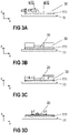
- a mask 30 having an even thickness is schematically illustrated in Figure 3A . That is, the mask 30 has an essentially even thickness in the vertical direction z.
- a thickness d30 of the mask 30 close to its edges may be the same as the thickness d32 of the mask 30 in regions further away from its edges.
- the thickness d30 of the mask 30 close to its edges may be even greater than the thickness d32 of the mask 30 in regions further away from its edges.
- An edge region of the mask 30 may be a region that is arranged within, e.g., 2mm or 4mm from an edge of the mask 30. That is, a width w30 of an edge region in a horizontal direction (e.g., first horizontal direction x) may be at least 2mm or at least 4mm.
- the resulting angle ⁇ between the top surface of the semiconductor substrate 10 and the edge of the mask 30 may be between 90 and 130°, for example.
- the following steps of forming the electrically conductive coating 20 and removing the mask 30 in Figures 3B and 3C are similar to what has been described with respect to Figures 2B and 2C above.
- the resulting electrically conductive coating 20 may have a thickness d1 of at least 300 to 1000nm in the vertical direction z.
- the resulting semiconductor substrate arrangement is schematically illustrated in Figure 3D .
- the first distance x1 may be 2mm, for example. Due to process irregularities or anomalies, however, small cavities or trenches 40 may be formed within the first distance x1 nevertheless (not specifically illustrated in Figure 3D ). Such small trenches or cavities 40, however, are much smaller than the cavities or trenches 40 that have been described with respect to Figure 2 above.
- any cavities or trenches 40 within the first distance x1 from the outer perimeter of the electrically conductive coating 20 have a maximum width w40 in a horizontal direction x, y or horizontal plane that is less than 10 ⁇ m and a maximum depth d40 in the vertical direction z that is less than 3 ⁇ m.
- Such small cavities or trenches 40 may store less or even no contaminants. Therefore, the risk of a fast oxidation during later processes is greatly reduced.
- FIG. 4A a mask 30 is schematically illustrated that is arranged on a semiconductor substrate 10, in particular on a first metallization layer 111. Through an opening in the mask 30, the first metallization layer 111 is visible. The edge of the mask 30, however, is uneven. That is, the edges of the mask do not form straight lines. This also results in unwanted cavities or trenches 40 when forming the electrically conductive coating 20 and removing the mask 30.
- Figure 4B illustrates the final state of the semiconductor substrate arrangement. The electrically conductive coating 20 is arranged on the semiconductor substrate 10 and the mask 30 has been removed from the semiconductor substrate 10.
- the edge of the mask 30 is formed evenly, as is schematically illustrated in Figure 5A , no cavities or trenches 40 or only small cavities or trenches 40 are formed in the first metallization layer 111, as is illustrated in Figure 5B .
- Small cavities or trenches 40 again refers to cavities or trenches 40 within the first distance x1 from the outer perimeter of the electrically conductive coating 20 that have a maximum width w40 in a horizontal direction x, y or horizontal plane that is less than 10 ⁇ m and a maximum depth d40 in the vertical direction z that is less than 3 ⁇ m.
- potential underetching of the mask 30 may be prevented. If such underetching occurs, e.g., in the example of Figure 4 , the first metallization layer 111 may be corrupted in the regions of the underetching which results in unwanted cavities and trenches 40.
- the mask 30 may be formed with an even thickness if a viscosity of the material forming the mask while applying the mask 30 to the semiconductor substrate 10 is chosen to be high enough to prevent unwanted smudging or smearing of the material.
- the viscosity depends on the material of the mask 30 and the temperature of the material while applying it to the semiconductor substrate 10. After applying the material to the semiconductor substrate 10, it may be hardened to a certain degree by removing at least part of the liquid, for the mask 30 to remain solid while forming the electrically conductive coating 20.
- the material of the mask 30 may also be chosen to have improved adhesion properties, in order to prevent unwanted lift off of the mask 30 during the process of forming the electrically conductive coating20.
- the material of the mask 30 may be chosen to have improved properties concerning the strip off process of the mask 30 (removal of the mask). That is, the mask may be easy to remove.
- the process parameters of the process of forming the mask 30 may be improved in order to guarantee an even thickness and even edges of the mask 30. That is, process parameters such as a process temperature may be optimized with regard to the material that is used to form the mask 30.
- a method for forming a semiconductor substrate arrangement may comprise forming a mask 30 on a semiconductor substrate 10, the semiconductor substrate 10 comprising a dielectric insulation layer 11, and a first metallization layer 111 arranged on the dielectric insulation layer 11.
- the mask 30 comprises at least one opening. That is, forming the mask 30 comprises forming the mask 30 only on some regions of the first metallization layer 111, while at least one region of the first metallization layer 111 remains free of the mask 30.
- the first metallization layer 111 is arranged between the mask 30 and the dielectric insulation layer. Forming the mask 30 comprises applying an essentially even layer of material on the first metallization layer 111.
- the material of the mask 30 may be applied to the first metallization layer 111 such that a thickness d30 adjacent to the edges of the mask 30 is greater than a thickness d32 of the mask 30 further away from the edges.
- the material may then be hardened in a subsequent step (e.g., removal of liquid from the material by performing a drying or heating process).
- At least one electrically conductive coating 20 is then formed on the first metallization layer 111.
- the at least one electrically conductive coating 20 is formed on those regions of the first metallization layer 111 that are not covered by the mask 30.
- a semiconductor substrate arrangement comprising a semiconductor substrate 10 comprising a dielectric insulation layer 11 and a first metallization layer 111 attached to the dielectric insulation layer 11, wherein the first metallization layer 111 is arranged on the dielectric insulation layer 11 in a vertical direction z.
- the resulting semiconductor substrate arrangement further comprises an electrically conductive coating 20 arranged on the first metallization layer 111 in the vertical direction z such that the first metallization layer 111 is arranged between the electrically conductive coating 20 and the dielectric insulation layer 11.
- the first metallization layer 111 does not comprise any cavities or trenches 40, or only cavities or trenches 40 having a width w40 in a horizontal direction x, y that is less than 10 ⁇ m and a depth d40 in the vertical direction z that is less than 3 ⁇ m.
Landscapes
- Chemical & Material Sciences (AREA)
- Engineering & Computer Science (AREA)
- Organic Chemistry (AREA)
- Materials Engineering (AREA)
- Mechanical Engineering (AREA)
- Metallurgy (AREA)
- Chemical Kinetics & Catalysis (AREA)
- Manufacturing & Machinery (AREA)
- Internal Circuitry In Semiconductor Integrated Circuit Devices (AREA)
- Physics & Mathematics (AREA)
- Geometry (AREA)
- Ceramic Engineering (AREA)
- Electrodes Of Semiconductors (AREA)
Claims (5)
- Verfahren zum Bilden einer Halbleitersubstratanordnung, aufweisend:Bilden einer Maske (30) auf einem Halbleitersubstrat (10), wobei das Halbleitersubstrat (10) eine dielektrische Isolierschicht (11), und eine erste Metallisierungsschicht (111) aufweist, die auf der dielektrischen Isolierschicht (11) angeordnet ist, und die Maske (30) mindestens eine Öffnung aufweist, wobei die erste Metallisierungsschicht (111) zwischen der Maske (30) und der dielektrischen Isolierschicht (11) angeordnet ist;Bilden einer Schicht einer elektrisch leitfähigen Beschichtung (20) auf der ersten Metallisierungsschicht (111), wobei die Schicht der elektrisch leitfähigen Beschichtung (20) in der mindestens einen Öffnung auf jenen Regionen der ersten Metallisierungsschicht (111) gebildet wird, die nicht von der Maske (30) bedeckt sind; undnach dem Bilden der Schicht der elektrisch leitfähigen Beschichtung (20), Entfernen der Maske (30) von dem Halbleitersubstrat (10), wobeidas Bilden der Maske (30) entweder das Aufbringen einer gleichförmigen Materialschicht auf die erste Metallisierungsschicht (111), so dass eine Dicke (d30) der Maske (30) in einer vertikalen Richtung (z) in einer Region benachbart zu den Rändern der Maske (30) gleich einer Dicke (d32) in der vertikalen Richtung (z) von Regionen der Maske (30) ist, die weiter entfernt von den Rändern liegen, oder das Aufbringen des Materials der Maske (30) auf die erste Metallisierungsschicht (111) aufweist, so dass die Dicke (d30) der Maske (30) in der Region benachbart zu den Rändern der Maske (30) größer als die Dicke (d32) der Regionen der Maske (30) ist, die weiter entfernt von den Rändern liegen, wobei die vertikale Richtung (z) senkrecht zu einer oberen Oberfläche des Halbleitersubstrats (10) ist;die Region benachbart zu den Rändern der Maske (30) eine Region ist, die innerhalb von 2 mm oder innerhalb von 4 mm zu einem Rand der Maske (30) angeordnet ist; unddie Maske (30) so gebildet ist, dass ein Winkel (α) zwischen einer obersten Oberfläche des Halbleitersubstrats (10) und dem Rand der Maske (30) zwischen 90 und 130° liegt.
- Verfahren nach Anspruch 1, das weiterhin das Härten des Materials der Maske (30) vor dem Bilden der Schicht der elektrisch leitfähigen Beschichtung (20) aufweist.
- Verfahren nach Anspruch 2, wobei das Härten des Materials der Maske (30) das Entfernen von Flüssigkeit aus dem Material aufweist, indem ein Trocknungs- oder Erwärmungsprozess durchgeführt wird.
- Verfahren nach einem der Ansprüche 1 bis 3, wobei die elektrisch leitfähige Beschichtung (20) mit einer Dicke (d1) von mindestens 300 bis 1000 nm in der vertikalen Richtung (z) gebildet wird.
- Verfahren nach einem der Ansprüche 1 bis 4, wobei das Entfernen der Maske (30) einen Ätzprozess aufweist.
Priority Applications (1)
| Application Number | Priority Date | Filing Date | Title |
|---|---|---|---|
| EP21151070.6A EP3889321B1 (de) | 2020-03-24 | 2020-03-24 | Verfahren zur herstellung einer halbleitersubstratanordnung |
Applications Claiming Priority (2)
| Application Number | Priority Date | Filing Date | Title |
|---|---|---|---|
| EP21151070.6A EP3889321B1 (de) | 2020-03-24 | 2020-03-24 | Verfahren zur herstellung einer halbleitersubstratanordnung |
| EP20165192.4A EP3885467A1 (de) | 2020-03-24 | 2020-03-24 | Halbleitersubstratanordnung |
Related Parent Applications (2)
| Application Number | Title | Priority Date | Filing Date |
|---|---|---|---|
| EP20165192.4A Division EP3885467A1 (de) | 2020-03-24 | 2020-03-24 | Halbleitersubstratanordnung |
| EP20165192.4A Division-Into EP3885467A1 (de) | 2020-03-24 | 2020-03-24 | Halbleitersubstratanordnung |
Publications (2)
| Publication Number | Publication Date |
|---|---|
| EP3889321A1 EP3889321A1 (de) | 2021-10-06 |
| EP3889321B1 true EP3889321B1 (de) | 2022-08-17 |
Family
ID=69960392
Family Applications (2)
| Application Number | Title | Priority Date | Filing Date |
|---|---|---|---|
| EP20165192.4A Withdrawn EP3885467A1 (de) | 2020-03-24 | 2020-03-24 | Halbleitersubstratanordnung |
| EP21151070.6A Active EP3889321B1 (de) | 2020-03-24 | 2020-03-24 | Verfahren zur herstellung einer halbleitersubstratanordnung |
Family Applications Before (1)
| Application Number | Title | Priority Date | Filing Date |
|---|---|---|---|
| EP20165192.4A Withdrawn EP3885467A1 (de) | 2020-03-24 | 2020-03-24 | Halbleitersubstratanordnung |
Country Status (3)
| Country | Link |
|---|---|
| US (1) | US12205826B2 (de) |
| EP (2) | EP3885467A1 (de) |
| CN (1) | CN113451143B (de) |
Family Cites Families (8)
| Publication number | Priority date | Publication date | Assignee | Title |
|---|---|---|---|---|
| DE4004844C1 (de) | 1990-02-16 | 1991-01-03 | Abb Ixys Semiconductor Gmbh | Verfahren zur Herstellung einer strukturierten Kupfermetallisierung auf einem Keramiksubstrat |
| DE102014211555B4 (de) * | 2014-06-17 | 2025-05-22 | Robert Bosch Gmbh | Verfahren zum Ausbilden einer Kavität und Bauelement mit einer Kavität |
| CN106960783B (zh) * | 2016-01-12 | 2020-03-10 | 中芯国际集成电路制造(上海)有限公司 | 一种半导体器件及其制备方法、电子装置 |
| DE102016118784A1 (de) * | 2016-10-04 | 2018-04-05 | Infineon Technologies Ag | Chipträger, konfiguriert zur delaminierungsfreien Kapselung und stabilen Sinterung |
| US10629540B2 (en) * | 2017-09-27 | 2020-04-21 | Taiwan Semiconductor Manufacturing Company, Ltd. | Semiconductor device and method |
| EP3518278A1 (de) * | 2018-01-30 | 2019-07-31 | Infineon Technologies AG | Leistungshalbleitermodul und verfahren zur dessen herstellung |
| EP3627546B1 (de) * | 2018-09-24 | 2024-10-30 | Infineon Technologies AG | Leistungshalbleitermodulanordnung |
| EP3644358B1 (de) * | 2018-10-25 | 2021-10-13 | Infineon Technologies AG | Leistungshalbleitermodulanordnung mit einem kontaktelement |
-
2020
- 2020-03-24 EP EP20165192.4A patent/EP3885467A1/de not_active Withdrawn
- 2020-03-24 EP EP21151070.6A patent/EP3889321B1/de active Active
-
2021
- 2021-03-16 US US17/202,849 patent/US12205826B2/en active Active
- 2021-03-23 CN CN202110308274.7A patent/CN113451143B/zh active Active
Also Published As
| Publication number | Publication date |
|---|---|
| US20210305062A1 (en) | 2021-09-30 |
| CN113451143A (zh) | 2021-09-28 |
| EP3889321A1 (de) | 2021-10-06 |
| CN113451143B (zh) | 2025-06-17 |
| US12205826B2 (en) | 2025-01-21 |
| EP3885467A1 (de) | 2021-09-29 |
Similar Documents
| Publication | Publication Date | Title |
|---|---|---|
| EP4050647B1 (de) | Verfahren zur herstellung von substratstruktur | |
| US10600658B2 (en) | Apparatus and method for bending a substrate | |
| EP2775516A2 (de) | Beanspruchungsausgleichsanordnung für Halbleitervorrichtungen mit einer oder mehreren doppelseitig mit Stanzgittern verbundenen Vorrichtungen, wobei die anderen Seiten der Stanzgitter mit AlN, Al2O3 oder Si3N4 Substraten verbunden sind | |
| JP5954374B2 (ja) | 絶縁基板、その製造方法、半導体モジュールおよび半導体装置 | |
| EP3889321B1 (de) | Verfahren zur herstellung einer halbleitersubstratanordnung | |
| US20160135293A1 (en) | Substrate structures and methods of manufacture | |
| EP4084062A1 (de) | Leistungshalbleitermodulanordnung | |
| US11282774B2 (en) | Power semiconductor module arrangement | |
| US20230369175A1 (en) | Power semiconductor module arrangement and method for producing the same | |
| EP4215508A1 (de) | Substrat und verfahren zur herstellung eines substrats | |
| EP3457434B1 (de) | Verfahren zur herstellung eines halbleitersubstrats für eine leistungshalbleitermodulanordnung | |
| CN111584422B (zh) | 半导体装置及其制造方法 | |
| EP4372807B1 (de) | Substratanordnung und verfahren zur herstellung einer substratanordnung | |
| EP4428914A1 (de) | Leistungshalbleitermodulanordnung | |
| US12482782B2 (en) | Bus bar, power semiconductor module arrangement including a bus bar, and method for producing a bus bar | |
| EP4576199A1 (de) | Substrat und verfahren zur herstellung eines substrats | |
| EP4346341A1 (de) | Verfahren zur herstellung einer leistungshalbleitermodulanordnung | |
| JPH09312356A (ja) | 半導体装置およびその製造方法 |
Legal Events
| Date | Code | Title | Description |
|---|---|---|---|
| PUAI | Public reference made under article 153(3) epc to a published international application that has entered the european phase |
Free format text: ORIGINAL CODE: 0009012 |
|
| STAA | Information on the status of an ep patent application or granted ep patent |
Free format text: STATUS: THE APPLICATION HAS BEEN PUBLISHED |
|
| AC | Divisional application: reference to earlier application |
Ref document number: 3885467 Country of ref document: EP Kind code of ref document: P |
|
| AK | Designated contracting states |
Kind code of ref document: A1 Designated state(s): AL AT BE BG CH CY CZ DE DK EE ES FI FR GB GR HR HU IE IS IT LI LT LU LV MC MK MT NL NO PL PT RO RS SE SI SK SM TR |
|
| STAA | Information on the status of an ep patent application or granted ep patent |
Free format text: STATUS: REQUEST FOR EXAMINATION WAS MADE |
|
| 17P | Request for examination filed |
Effective date: 20211011 |
|
| RBV | Designated contracting states (corrected) |
Designated state(s): AL AT BE BG CH CY CZ DE DK EE ES FI FR GB GR HR HU IE IS IT LI LT LU LV MC MK MT NL NO PL PT RO RS SE SI SK SM TR |
|
| GRAP | Despatch of communication of intention to grant a patent |
Free format text: ORIGINAL CODE: EPIDOSNIGR1 |
|
| STAA | Information on the status of an ep patent application or granted ep patent |
Free format text: STATUS: GRANT OF PATENT IS INTENDED |
|
| INTG | Intention to grant announced |
Effective date: 20220405 |
|
| GRAS | Grant fee paid |
Free format text: ORIGINAL CODE: EPIDOSNIGR3 |
|
| GRAA | (expected) grant |
Free format text: ORIGINAL CODE: 0009210 |
|
| STAA | Information on the status of an ep patent application or granted ep patent |
Free format text: STATUS: THE PATENT HAS BEEN GRANTED |
|
| AC | Divisional application: reference to earlier application |
Ref document number: 3885467 Country of ref document: EP Kind code of ref document: P |
|
| AK | Designated contracting states |
Kind code of ref document: B1 Designated state(s): AL AT BE BG CH CY CZ DE DK EE ES FI FR GB GR HR HU IE IS IT LI LT LU LV MC MK MT NL NO PL PT RO RS SE SI SK SM TR |
|
| REG | Reference to a national code |
Ref country code: CH Ref legal event code: EP |
|
| REG | Reference to a national code |
Ref country code: DE Ref legal event code: R096 Ref document number: 602020004605 Country of ref document: DE |
|
| REG | Reference to a national code |
Ref country code: IE Ref legal event code: FG4D |
|
| REG | Reference to a national code |
Ref country code: AT Ref legal event code: REF Ref document number: 1512222 Country of ref document: AT Kind code of ref document: T Effective date: 20220915 |
|
| REG | Reference to a national code |
Ref country code: NL Ref legal event code: MP Effective date: 20220817 |
|
| REG | Reference to a national code |
Ref country code: LT Ref legal event code: MG9D |
|
| PG25 | Lapsed in a contracting state [announced via postgrant information from national office to epo] |
Ref country code: SE Free format text: LAPSE BECAUSE OF FAILURE TO SUBMIT A TRANSLATION OF THE DESCRIPTION OR TO PAY THE FEE WITHIN THE PRESCRIBED TIME-LIMIT Effective date: 20220817 Ref country code: RS Free format text: LAPSE BECAUSE OF FAILURE TO SUBMIT A TRANSLATION OF THE DESCRIPTION OR TO PAY THE FEE WITHIN THE PRESCRIBED TIME-LIMIT Effective date: 20220817 Ref country code: PT Free format text: LAPSE BECAUSE OF FAILURE TO SUBMIT A TRANSLATION OF THE DESCRIPTION OR TO PAY THE FEE WITHIN THE PRESCRIBED TIME-LIMIT Effective date: 20221219 Ref country code: NO Free format text: LAPSE BECAUSE OF FAILURE TO SUBMIT A TRANSLATION OF THE DESCRIPTION OR TO PAY THE FEE WITHIN THE PRESCRIBED TIME-LIMIT Effective date: 20221117 Ref country code: NL Free format text: LAPSE BECAUSE OF FAILURE TO SUBMIT A TRANSLATION OF THE DESCRIPTION OR TO PAY THE FEE WITHIN THE PRESCRIBED TIME-LIMIT Effective date: 20220817 Ref country code: LV Free format text: LAPSE BECAUSE OF FAILURE TO SUBMIT A TRANSLATION OF THE DESCRIPTION OR TO PAY THE FEE WITHIN THE PRESCRIBED TIME-LIMIT Effective date: 20220817 Ref country code: LT Free format text: LAPSE BECAUSE OF FAILURE TO SUBMIT A TRANSLATION OF THE DESCRIPTION OR TO PAY THE FEE WITHIN THE PRESCRIBED TIME-LIMIT Effective date: 20220817 Ref country code: FI Free format text: LAPSE BECAUSE OF FAILURE TO SUBMIT A TRANSLATION OF THE DESCRIPTION OR TO PAY THE FEE WITHIN THE PRESCRIBED TIME-LIMIT Effective date: 20220817 |
|
| REG | Reference to a national code |
Ref country code: AT Ref legal event code: MK05 Ref document number: 1512222 Country of ref document: AT Kind code of ref document: T Effective date: 20220817 |
|
| PG25 | Lapsed in a contracting state [announced via postgrant information from national office to epo] |
Ref country code: PL Free format text: LAPSE BECAUSE OF FAILURE TO SUBMIT A TRANSLATION OF THE DESCRIPTION OR TO PAY THE FEE WITHIN THE PRESCRIBED TIME-LIMIT Effective date: 20220817 Ref country code: IS Free format text: LAPSE BECAUSE OF FAILURE TO SUBMIT A TRANSLATION OF THE DESCRIPTION OR TO PAY THE FEE WITHIN THE PRESCRIBED TIME-LIMIT Effective date: 20221217 Ref country code: HR Free format text: LAPSE BECAUSE OF FAILURE TO SUBMIT A TRANSLATION OF THE DESCRIPTION OR TO PAY THE FEE WITHIN THE PRESCRIBED TIME-LIMIT Effective date: 20220817 Ref country code: GR Free format text: LAPSE BECAUSE OF FAILURE TO SUBMIT A TRANSLATION OF THE DESCRIPTION OR TO PAY THE FEE WITHIN THE PRESCRIBED TIME-LIMIT Effective date: 20221118 |
|
| PG25 | Lapsed in a contracting state [announced via postgrant information from national office to epo] |
Ref country code: SM Free format text: LAPSE BECAUSE OF FAILURE TO SUBMIT A TRANSLATION OF THE DESCRIPTION OR TO PAY THE FEE WITHIN THE PRESCRIBED TIME-LIMIT Effective date: 20220817 Ref country code: RO Free format text: LAPSE BECAUSE OF FAILURE TO SUBMIT A TRANSLATION OF THE DESCRIPTION OR TO PAY THE FEE WITHIN THE PRESCRIBED TIME-LIMIT Effective date: 20220817 Ref country code: ES Free format text: LAPSE BECAUSE OF FAILURE TO SUBMIT A TRANSLATION OF THE DESCRIPTION OR TO PAY THE FEE WITHIN THE PRESCRIBED TIME-LIMIT Effective date: 20220817 Ref country code: DK Free format text: LAPSE BECAUSE OF FAILURE TO SUBMIT A TRANSLATION OF THE DESCRIPTION OR TO PAY THE FEE WITHIN THE PRESCRIBED TIME-LIMIT Effective date: 20220817 Ref country code: CZ Free format text: LAPSE BECAUSE OF FAILURE TO SUBMIT A TRANSLATION OF THE DESCRIPTION OR TO PAY THE FEE WITHIN THE PRESCRIBED TIME-LIMIT Effective date: 20220817 Ref country code: AT Free format text: LAPSE BECAUSE OF FAILURE TO SUBMIT A TRANSLATION OF THE DESCRIPTION OR TO PAY THE FEE WITHIN THE PRESCRIBED TIME-LIMIT Effective date: 20220817 |
|
| REG | Reference to a national code |
Ref country code: DE Ref legal event code: R097 Ref document number: 602020004605 Country of ref document: DE |
|
| PG25 | Lapsed in a contracting state [announced via postgrant information from national office to epo] |
Ref country code: SK Free format text: LAPSE BECAUSE OF FAILURE TO SUBMIT A TRANSLATION OF THE DESCRIPTION OR TO PAY THE FEE WITHIN THE PRESCRIBED TIME-LIMIT Effective date: 20220817 Ref country code: EE Free format text: LAPSE BECAUSE OF FAILURE TO SUBMIT A TRANSLATION OF THE DESCRIPTION OR TO PAY THE FEE WITHIN THE PRESCRIBED TIME-LIMIT Effective date: 20220817 |
|
| PLBE | No opposition filed within time limit |
Free format text: ORIGINAL CODE: 0009261 |
|
| STAA | Information on the status of an ep patent application or granted ep patent |
Free format text: STATUS: NO OPPOSITION FILED WITHIN TIME LIMIT |
|
| PG25 | Lapsed in a contracting state [announced via postgrant information from national office to epo] |
Ref country code: AL Free format text: LAPSE BECAUSE OF FAILURE TO SUBMIT A TRANSLATION OF THE DESCRIPTION OR TO PAY THE FEE WITHIN THE PRESCRIBED TIME-LIMIT Effective date: 20220817 |
|
| P01 | Opt-out of the competence of the unified patent court (upc) registered |
Effective date: 20230528 |
|
| 26N | No opposition filed |
Effective date: 20230519 |
|
| PG25 | Lapsed in a contracting state [announced via postgrant information from national office to epo] |
Ref country code: SI Free format text: LAPSE BECAUSE OF FAILURE TO SUBMIT A TRANSLATION OF THE DESCRIPTION OR TO PAY THE FEE WITHIN THE PRESCRIBED TIME-LIMIT Effective date: 20220817 |
|
| PG25 | Lapsed in a contracting state [announced via postgrant information from national office to epo] |
Ref country code: MC Free format text: LAPSE BECAUSE OF FAILURE TO SUBMIT A TRANSLATION OF THE DESCRIPTION OR TO PAY THE FEE WITHIN THE PRESCRIBED TIME-LIMIT Effective date: 20220817 |
|
| REG | Reference to a national code |
Ref country code: CH Ref legal event code: PL |
|
| REG | Reference to a national code |
Ref country code: BE Ref legal event code: MM Effective date: 20230331 |
|
| PG25 | Lapsed in a contracting state [announced via postgrant information from national office to epo] |
Ref country code: LU Free format text: LAPSE BECAUSE OF NON-PAYMENT OF DUE FEES Effective date: 20230324 |
|
| REG | Reference to a national code |
Ref country code: IE Ref legal event code: MM4A |
|
| PG25 | Lapsed in a contracting state [announced via postgrant information from national office to epo] |
Ref country code: LI Free format text: LAPSE BECAUSE OF NON-PAYMENT OF DUE FEES Effective date: 20230331 Ref country code: IE Free format text: LAPSE BECAUSE OF NON-PAYMENT OF DUE FEES Effective date: 20230324 Ref country code: FR Free format text: LAPSE BECAUSE OF NON-PAYMENT OF DUE FEES Effective date: 20230331 Ref country code: CH Free format text: LAPSE BECAUSE OF NON-PAYMENT OF DUE FEES Effective date: 20230331 |
|
| PG25 | Lapsed in a contracting state [announced via postgrant information from national office to epo] |
Ref country code: BE Free format text: LAPSE BECAUSE OF NON-PAYMENT OF DUE FEES Effective date: 20230331 |
|
| PG25 | Lapsed in a contracting state [announced via postgrant information from national office to epo] |
Ref country code: IT Free format text: LAPSE BECAUSE OF FAILURE TO SUBMIT A TRANSLATION OF THE DESCRIPTION OR TO PAY THE FEE WITHIN THE PRESCRIBED TIME-LIMIT Effective date: 20220817 |
|
| PG25 | Lapsed in a contracting state [announced via postgrant information from national office to epo] |
Ref country code: BG Free format text: LAPSE BECAUSE OF FAILURE TO SUBMIT A TRANSLATION OF THE DESCRIPTION OR TO PAY THE FEE WITHIN THE PRESCRIBED TIME-LIMIT Effective date: 20220817 |
|
| GBPC | Gb: european patent ceased through non-payment of renewal fee |
Effective date: 20240324 |
|
| PG25 | Lapsed in a contracting state [announced via postgrant information from national office to epo] |
Ref country code: BG Free format text: LAPSE BECAUSE OF FAILURE TO SUBMIT A TRANSLATION OF THE DESCRIPTION OR TO PAY THE FEE WITHIN THE PRESCRIBED TIME-LIMIT Effective date: 20220817 |
|
| PG25 | Lapsed in a contracting state [announced via postgrant information from national office to epo] |
Ref country code: GB Free format text: LAPSE BECAUSE OF NON-PAYMENT OF DUE FEES Effective date: 20240324 |
|
| PG25 | Lapsed in a contracting state [announced via postgrant information from national office to epo] |
Ref country code: GB Free format text: LAPSE BECAUSE OF NON-PAYMENT OF DUE FEES Effective date: 20240324 |
|
| PGFP | Annual fee paid to national office [announced via postgrant information from national office to epo] |
Ref country code: DE Payment date: 20250521 Year of fee payment: 6 |
|
| PG25 | Lapsed in a contracting state [announced via postgrant information from national office to epo] |
Ref country code: CY Free format text: LAPSE BECAUSE OF FAILURE TO SUBMIT A TRANSLATION OF THE DESCRIPTION OR TO PAY THE FEE WITHIN THE PRESCRIBED TIME-LIMIT; INVALID AB INITIO Effective date: 20200324 |
|
| PG25 | Lapsed in a contracting state [announced via postgrant information from national office to epo] |
Ref country code: HU Free format text: LAPSE BECAUSE OF FAILURE TO SUBMIT A TRANSLATION OF THE DESCRIPTION OR TO PAY THE FEE WITHIN THE PRESCRIBED TIME-LIMIT; INVALID AB INITIO Effective date: 20200324 |
|
| PG25 | Lapsed in a contracting state [announced via postgrant information from national office to epo] |
Ref country code: TR Free format text: LAPSE BECAUSE OF FAILURE TO SUBMIT A TRANSLATION OF THE DESCRIPTION OR TO PAY THE FEE WITHIN THE PRESCRIBED TIME-LIMIT Effective date: 20220817 |