EP3893232A1 - Structure de pixels, panneau d'affichage et appareil d'affichage - Google Patents
Structure de pixels, panneau d'affichage et appareil d'affichage Download PDFInfo
- Publication number
- EP3893232A1 EP3893232A1 EP20846067.5A EP20846067A EP3893232A1 EP 3893232 A1 EP3893232 A1 EP 3893232A1 EP 20846067 A EP20846067 A EP 20846067A EP 3893232 A1 EP3893232 A1 EP 3893232A1
- Authority
- EP
- European Patent Office
- Prior art keywords
- pixel
- sub
- chip
- virtual
- same
- Prior art date
- Legal status (The legal status is an assumption and is not a legal conclusion. Google has not performed a legal analysis and makes no representation as to the accuracy of the status listed.)
- Pending
Links
Images



Classifications
-
- H—ELECTRICITY
- H10—SEMICONDUCTOR DEVICES; ELECTRIC SOLID-STATE DEVICES NOT OTHERWISE PROVIDED FOR
- H10H—INORGANIC LIGHT-EMITTING SEMICONDUCTOR DEVICES HAVING POTENTIAL BARRIERS
- H10H29/00—Integrated devices, or assemblies of multiple devices, comprising at least one light-emitting semiconductor element covered by group H10H20/00
- H10H29/10—Integrated devices comprising at least one light-emitting semiconductor component covered by group H10H20/00
- H10H29/14—Integrated devices comprising at least one light-emitting semiconductor component covered by group H10H20/00 comprising multiple light-emitting semiconductor components
- H10H29/142—Two-dimensional arrangements, e.g. asymmetric LED layout
-
- H—ELECTRICITY
- H10—SEMICONDUCTOR DEVICES; ELECTRIC SOLID-STATE DEVICES NOT OTHERWISE PROVIDED FOR
- H10W—GENERIC PACKAGES, INTERCONNECTIONS, CONNECTORS OR OTHER CONSTRUCTIONAL DETAILS OF DEVICES COVERED BY CLASS H10
- H10W90/00—Package configurations
-
- H—ELECTRICITY
- H10—SEMICONDUCTOR DEVICES; ELECTRIC SOLID-STATE DEVICES NOT OTHERWISE PROVIDED FOR
- H10H—INORGANIC LIGHT-EMITTING SEMICONDUCTOR DEVICES HAVING POTENTIAL BARRIERS
- H10H20/00—Individual inorganic light-emitting semiconductor devices having potential barriers, e.g. light-emitting diodes [LED]
- H10H20/80—Constructional details
- H10H20/85—Packages
- H10H20/8506—Containers
-
- H—ELECTRICITY
- H10—SEMICONDUCTOR DEVICES; ELECTRIC SOLID-STATE DEVICES NOT OTHERWISE PROVIDED FOR
- H10H—INORGANIC LIGHT-EMITTING SEMICONDUCTOR DEVICES HAVING POTENTIAL BARRIERS
- H10H20/00—Individual inorganic light-emitting semiconductor devices having potential barriers, e.g. light-emitting diodes [LED]
- H10H20/80—Constructional details
- H10H20/85—Packages
- H10H20/857—Interconnections, e.g. lead-frames, bond wires or solder balls
-
- G—PHYSICS
- G09—EDUCATION; CRYPTOGRAPHY; DISPLAY; ADVERTISING; SEALS
- G09G—ARRANGEMENTS OR CIRCUITS FOR CONTROL OF INDICATING DEVICES USING STATIC MEANS TO PRESENT VARIABLE INFORMATION
- G09G2300/00—Aspects of the constitution of display devices
- G09G2300/04—Structural and physical details of display devices
- G09G2300/0439—Pixel structures
- G09G2300/0452—Details of colour pixel setup, e.g. pixel composed of a red, a blue and two green components
-
- G—PHYSICS
- G09—EDUCATION; CRYPTOGRAPHY; DISPLAY; ADVERTISING; SEALS
- G09G—ARRANGEMENTS OR CIRCUITS FOR CONTROL OF INDICATING DEVICES USING STATIC MEANS TO PRESENT VARIABLE INFORMATION
- G09G3/00—Control arrangements or circuits, of interest only in connection with visual indicators other than cathode-ray tubes
- G09G3/20—Control arrangements or circuits, of interest only in connection with visual indicators other than cathode-ray tubes for presentation of an assembly of a number of characters, e.g. a page, by composing the assembly by combination of individual elements arranged in a matrix no fixed position being assigned to or needed to be assigned to the individual characters or partial characters
- G09G3/22—Control arrangements or circuits, of interest only in connection with visual indicators other than cathode-ray tubes for presentation of an assembly of a number of characters, e.g. a page, by composing the assembly by combination of individual elements arranged in a matrix no fixed position being assigned to or needed to be assigned to the individual characters or partial characters using controlled light sources
- G09G3/30—Control arrangements or circuits, of interest only in connection with visual indicators other than cathode-ray tubes for presentation of an assembly of a number of characters, e.g. a page, by composing the assembly by combination of individual elements arranged in a matrix no fixed position being assigned to or needed to be assigned to the individual characters or partial characters using controlled light sources using electroluminescent panels
- G09G3/32—Control arrangements or circuits, of interest only in connection with visual indicators other than cathode-ray tubes for presentation of an assembly of a number of characters, e.g. a page, by composing the assembly by combination of individual elements arranged in a matrix no fixed position being assigned to or needed to be assigned to the individual characters or partial characters using controlled light sources using electroluminescent panels semiconductive, e.g. using light-emitting diodes [LED]
-
- H—ELECTRICITY
- H10—SEMICONDUCTOR DEVICES; ELECTRIC SOLID-STATE DEVICES NOT OTHERWISE PROVIDED FOR
- H10K—ORGANIC ELECTRIC SOLID-STATE DEVICES
- H10K59/00—Integrated devices, or assemblies of multiple devices, comprising at least one organic light-emitting element covered by group H10K50/00
- H10K59/30—Devices specially adapted for multicolour light emission
- H10K59/35—Devices specially adapted for multicolour light emission comprising red-green-blue [RGB] subpixels
- H10K59/353—Devices specially adapted for multicolour light emission comprising red-green-blue [RGB] subpixels characterised by the geometrical arrangement of the RGB subpixels
Definitions
- the present application relates to the technical field of display, and in particular to a pixel structure, a display panel, and a display device.
- a COB (chip on board) display panel on the market generally has a pixel pitch of 2 mm.
- the pixel pitch In order to improve the resolution of the display panel, it is necessary to reduce the pixel pitch, which in turn needs to use more pixels and leads to increased cost.
- the conventional technology it is difficult to reduce the pixel pitch to 0.9 mm or less.
- the present application provides a high-resolution pixel structure, a display panel, and a display device.
- a pixel structure comprising a plurality of pixel groups arranged in an array to form an array structure and each comprising a first sub-pixel, a second sub-pixel and a third sub-pixel in a ratio of 1:1:1; in each of the pixel groups, a line connecting the centers of the first sub-pixel, the second sub-pixel and the third sub-pixel forms a first virtual isosceles right triangle; the second sub-pixel constitutes the right-angle vertex of the first virtual isosceles right triangle, and the first sub-pixel, the second sub-pixel, and the third sub-pixel in each pixel group are arranged in the same manner; wherein in every two adjacent pixel groups in a same row of the array structure, a line connecting the centers of the second sub-pixel and the third sub-pixel of one pixel group and the first sub-pixel of the other pixel group forms a second virtual isosceles right triangle; and in every two adjacent pixel groups in a same column of the array structure, a
- the above pixel structure uses the "virtual pixel” technology (i.e., a technology that uses the persistence of human eyes to time-multiplex real pixels to reproduce more virtual pixels).
- virtual pixel i.e., a technology that uses the persistence of human eyes to time-multiplex real pixels to reproduce more virtual pixels.
- a display panel comprising the pixel structure as described above.
- a display panel comprising a circuit board, and a plurality of pixel groups arranged in an array to form an array structure; each pixel group comprises a first chip, a second chip and a third chip in a ratio of 2:1:1, and the first chip, the second chip and the third chip are formed on a same side of the circuit board; in each pixel group, the first chip, the second chip and the third chip are at four vertices of a virtual square, respectively, and all the first chips are at two vertices on one diagonal of the virtual square; and the first chip, the second chip, and the third chip in each pixel group are arranged in the same manner.
- a display device comprising the display panel as described above.
- first and second in the present application do not denote a particular quantity or order, but merely serve to distinguish between names.
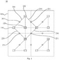
- an embodiment of the present application relates to a pixel structure 10 comprising a plurality of pixel groups 100 arranged in an array and each comprising a first sub-pixel 110, a second sub-pixel 120, and a third sub-pixel 130 in a ratio of 1:1:1.
- each pixel group 100 comprises one first sub-pixel 110, one second sub-pixel 120, and one third sub-pixel 130
- each of the first sub-pixel 110, the second sub-pixel 120 and the third sub-pixel 130 is a red light emitting chip, a blue light emitting chip, or a green light emitting chip
- the first sub-pixel 110, the second sub-pixel 120, and the third sub-pixel 130 emit light of different colors.
- the first sub-pixel 110, the second sub-pixel 120, or the third sub-pixel 130 may emit light of colors other than red, blue, and green.
- the first sub-pixel 110 and the second sub-pixel 120 are arranged in a first direction
- the second sub-pixel 120 and the third sub-pixel 130 are arranged in a second direction
- a line connecting the centers of the first sub-pixel 110, the second sub-pixel 120 and the third sub-pixel 130 forms a first virtual isosceles right triangle 200.
- the centers of the first sub-pixel 110, the second sub-pixel 120, and the third sub-pixel 130 constitute the three vertices of the first virtual isosceles right triangle 200, respectively.
- the second sub-pixel 120 constitutes the right-angle vertex of the first virtual isosceles right angle triangle 200.
- a line connecting the centers of the second sub-pixel 120 and the third sub-pixel 130 of one pixel group 100 and the first sub-pixel 110 of the other pixel group 100 forms a second virtual isosceles right triangle 210; and in every two adjacent pixel groups 100 in a same column of the array structure, a line connecting the centers of the first sub-pixel 110 and the second sub-pixel 120 of one pixel group 100 and the third sub-pixel 130 of the other pixel group 100 forms a third virtual isosceles right triangle 220.
- a line connecting the centers of the second sub-pixel 120 of one pixel group 100, the first sub-pixel 110 of a pixel group 100 adjacent to the aforementioned pixel group 100 in the row direction of the array structure, and the third sub-pixel 130 of a pixel group 100 adjacent to the aforementioned pixel group 100 in the column direction of the array structure forms a fourth virtual isosceles right triangle 230.
- a line connecting the centers of the first sub-pixel 110, the second sub-pixel 120 and the third sub-pixel 130 of a pixel group 100 in line 1 forms a first virtual isosceles right triangle 200; a line connecting the centers of the second sub-pixel 120 and the third sub-pixel 130 of the pixel group 100 in line 1, column 1 and the first sub-pixel 110 of a pixel group 100 in line 1, column 2 forms a second virtual isosceles right triangle 210; a line connecting the centers of the first sub-pixel 110 and the second sub-pixel 120 of the pixel group 100 in line 1, column 1 and the third sub-pixel 130 of a pixel group 100 in line 2, column 1 forms a third virtual isosceles right triangle 220; and a line connecting the centers of the second sub-pixel 120 of the pixel group 100 in line 1, column 1, the first sub-pixel 110 of the pixel group 100 in line 1, column 2, and the third sub-pixel 130 in the pixel group
- the above pixel structure uses the "virtual pixel” technology (i.e., a technology that uses the persistence of human eyes to time-multiplex real pixels to reproduce more virtual pixels).
- a first pixel 201 is formed at the circumcenter of the first virtual isosceles right triangle 200
- a second pixel 211 is formed at the circumcenter of the second virtual isosceles right triangle 210
- a third pixel 221 is formed at the circumcenter of the third virtual isosceles right triangle 220
- a fourth pixel 231 is formed at the circumcenter of the fourth virtual isosceles right triangle 230.
- the pixel structure 10 when the pixel structure 10 is applied to a display panel, under the condition that the display panel has the same number of sub-pixels as a real pixel display panel, the resolution of the display panel can be improved, and therefore the cost of the display panel is reduced.
- a plurality of pixel groups 100 are arranged in an array to form an array structure, all the pixel groups 100 in the array structure are arranged at even intervals in a row direction, and all the pixel groups 100 in the array structure are arranged at even intervals in a column direction. In this way, all the pixel groups 100 in the entire pixel structure 10 are uniformly arranged, thereby ensuring the uniformity of light emission.
- the first direction is consistent with the row direction of the array structure
- the second direction is consistent with the column direction of the array structure
- the first sub-pixels 110 and the second sub-pixels 120 of all pixel groups 100 in a same row of the array structure are in a same straight line
- the third sub-pixels 130 of all pixel groups 100 in a same row are in a same straight line
- the second sub-pixels 120 and the third sub-pixels 130 of all pixel groups 100 in a same column of the array structure are in a same straight line
- the first sub-pixels 110 in all pixel groups 100 in a same column are in a same straight line.
- the circumcenters of all first virtual isosceles right triangles 200 in a same row of the array structure are in a same straight line; and the circumcenters of all first virtual isosceles right triangles 200 in a same column of the array structure are in a same straight line.
- all the first pixels 201 which may be formed by the pixel structure 10 are in array arrangement, and the first pixels 201 in a same row in the pixel structure 10 are in a same straight line, and the first pixels 201 in a same column are in a same straight line, so that the first pixels 201 are uniformly distributed, thereby ensuring the uniformity of light emission.
- a line connecting the circumcenters of every two adjacent first virtual isosceles right triangles 200 in a same row of the array structure is consistent in length; and a line connecting the circumcenters of every two adjacent first virtual isosceles right triangles 200 in a same column of the array structure is consistent in length.
- the length of the line connecting the circumcenters of every two adjacent first virtual isosceles right triangles 200 in a same row of the array structure is twice the length of a right-angle side of the first virtual isosceles right triangle 200. Therefore, in two adjacent pixel groups 100 in a same row, a line connecting the centers of the second sub-pixel 120 and the third sub-pixel 130 of the left pixel group 100 and the first sub-pixel 110 of the right pixel group 100 may form a second virtual isosceles right triangle 210, and a second pixel 211 may be formed at the circumcenter of the second virtual isosceles right triangle 210.
- the length of the line connecting the circumcenters of every two adjacent first virtual isosceles right triangles 200 in a same column of the array structure are twice the length of a right-angle side of the first virtual isosceles right triangle. Therefore, in two adjacent pixel groups 100 in a same column, a line connecting the centers of the first sub-pixel 110 and the second sub-pixel 120 of the upper pixel group 100 and the third sub-pixel 130 of the lower pixel group 100 may form a third virtual isosceles right triangle 220, and a third pixel 221 may be formed at the circumcenter of the third virtual isosceles right triangle 220.
- the above pixel structure uses the "virtual pixel” technology (i.e., a technology that uses the persistence of human eyes to time-multiplex real pixels to reproduce more virtual pixels).
- a first pixel 201 is formed at the circumcenter of the first virtual isosceles right triangle 200; a second pixel 211 is formed at the circumcenter of the second virtual isosceles right triangle 210; a third pixel 221 is formed at the circumcenter of the third virtual isosceles right triangle 220; and a fourth pixel 231 is formed at the circumcenter of the fourth virtual isosceles right triangle 230.
- the pixel structure 10 when the pixel structure 10 is applied to a display panel, under the condition that the display panel has the same number of sub-pixels as a real pixel display panel, the resolution of the display panel can be improved, and therefore the cost of the display panel is reduced.
- each pixel group may further comprises a fourth sub-pixel 140, where the centers of the first sub-pixel 110, the second sub-pixel 120, the third sub-pixel 130 and the fourth sub-pixel 140 are at four vertices of a virtual square, respectively, and two sub-pixels at two vertices on one diagonal of the virtual square emit light of same color.
- the second sub-pixel 120 and the fourth sub-pixel 140 emit light of the same color.
- the above pixel structure uses the "virtual pixel" technology (i.e., a technology that uses the persistence of human eyes to time-multiplex real pixels to reproduce more virtual pixels).
- the first pixel 201 is approximately at the geometric center of a virtual square formed by the first sub-pixel 110, the second sub-pixel 120, the third sub-pixel 130, and the fourth sub-pixel 140 as vertices.
- each of the first sub-pixel 110, the second sub-pixel 120, and the third sub-pixel 130 is a red light emitting chip, a blue light emitting chip, or a green light emitting chip
- the first sub-pixel 110, the second sub-pixel 120, and the third sub-pixel 130 emit light of different colors
- the second sub-pixel 120 and the fourth sub-pixel 140 emit light of the same color. Therefore, when the pixel structure 10 displays a single color, it is displayed in a straight line, the centers of any two colors displayed mixedly are in a straight line, and the centers of the three colors displayed mixedly are aligned.
- the sub-pixels that emit light of the same color at two vertices on one diagonal of the virtual square needs not to be lighted at the same time, and more pixels can be displayed by controlling time division multiplexing of the sub-pixels of the pixel group 100.
- the side length d0 of the virtual square formed by the first sub-pixel 110, the second sub-pixel 120, the third sub-pixel 130, and the fourth sub-pixel 140 as vertices ranges from 0.4 mm to 3 mm. Since the distance between the geometric centers of adjacent two pixel groups 100 is twice the side length of the virtual square, the pitch between real pixels may be 0.8 mm at the minimum, which is less than 0.9 mm, thereby obtaining a smaller pixel pitch.
- An embodiment of the present application further relates to a display panel comprising the pixel structure 10 described above.
- the display panel may be an OLED (Organic Light-Emitting Diode) display panel, a COB display panel, an LED (Light Emitting Diode) display panel, or the like.
- OLED Organic Light-Emitting Diode
- COB COB
- LED Light Emitting Diode
- the display panel is a COB display panel
- the first sub-pixel 110, the second sub-pixel 120, and the third sub-pixel 130 may be face-up or flip-chip light emitting chips.
- an embodiment of the present application further relates to a display panel.
- the display panel comprises a circuit board, and a plurality of pixel groups arranged in an array to form an array structure.
- Each pixel group comprises a first chip, a second chip and a third chip in a ratio of 2:1:1, and the first chip, the second chip and the third chip are formed on a same side of the circuit board through molding; in each pixel group, the first chip, the second chip and the third chip are at four vertices of a virtual square, respectively, and all the first chips are at two vertices on one diagonal of the virtual square; and the first chip, the second chip, and the third chip in each pixel group are arranged in the same manner.
- the circuit board may be a PCB circuit board on which a plurality of pixel groups with the same internal arrangement are provided.
- FIG. 3 shows a schematic diagram of a pixel structure of a display panel according to an embodiment.
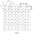
- FIG. 4 shows a schematic diagram of a pixel structure of a display panel according to another embodiment.
- each pixel group 100 comprises two first chips 111, one second chip 112, and one third chip 113.
- each pixel group 100 comprises four first chips 111, two second chips 112, and two third chips 113, as long as it is guaranteed that the first chips 111, the second chips 112 and the third chips 113 are in a ratio of 2:1:1.
- Each of the first chip 111, the second chip 112, and the third chip 113 may be a red light emitting chip, a blue light emitting chip, or a green light emitting chip, and the first chip 111, the second chip 112, and the third chip 113 emit light of different colors.
- the first chip 111 is a green light emitting chip
- the second chip 112 is a red light emitting chip
- the third chip 113 is a blue light emitting chip.
- the green light emitting chip, the red light emitting chip, and the blue light emitting chip are in a ratio of 2:1:1.
- the second chip 112 is a blue light emitting chip
- the third chip 113 is a red light emitting chip.
- the first chip 111 is a red light emitting chip
- the second chip 112 is a green light emitting chip
- the third chip 113 is a blue light emitting chip.
- the red light emitting chip, the green light emitting chip, and the blue light emitting chip are in a ratio of 2:1:1.
- the second chip 112 is a blue light emitting chip
- the third chip 113 is a green light emitting chip.
- the first chip 111 is a blue light emitting chip
- the second chip 112 is a red light emitting chip
- the third chip 113 is a green light emitting chip.
- the blue light emitting chip, the red light emitting chip, and the green light emitting chip are in a ratio of 2:1:1.
- the second chip 112 is a green light emitting chip
- the third chip 113 is a red light emitting chip.
- first chip 111, the second chip 112, and the third chip 113 may be light emitting chips of other colors.
- the first chip 111, the second chip 112, and the third chip 113 therein are formed on a same side of the PCB board through molding.
- the two first chips 111, one second chip 112 and one third chip 113 are at four vertices of a virtual square
- the two first chips 111 are at two vertices on one diagonal of the virtual square, respectively
- one second chip 112 and one third chip 113 are at two vertices on the other diagonal line of the virtual square, respectively.
- the two first chips 111 in one pixel group are not lighted at the same time, and more pixels may be displayed by controlling time-division multiplexing of the chips in the pixel group 100.
- each pixel group 100 may display a first virtual pixel 114 by controlling one of the first chips 111, one second chip 112, and one third chip 113.
- the first virtual pixel 114 is approximately at the geometric center of the virtual square formed by two first chips 111, one second chip 112 and one third chip 113 as vertices in the pixel group 100.
- the two adjacent pixel groups 100 display a second virtual pixel 115 by multiplexing real pixels, for example, lighting the first chip 111 and the third chip 113 of the left pixel group 100 and lighting the second chip 112 of the right pixel group 100, and the second virtual pixel 115 may be approximately at the circumcenter of the virtual triangle with the three chips as vertices, and of course, the second virtual pixel 115 may also be located inside the virtual triangle.
- each pixel group 100 may display a first virtual pixel 114 by controlling one of the first chips 111, one second chip 112, and one third chip 113.
- the first virtual pixel 114 is approximately at the geometric center of the virtual square formed by two first chips 111, one second chip 112 and one third chip 113 as vertices in the pixel group 100.
- the two adjacent pixel groups 100 display a second virtual pixel 115 by multiplexing real pixels, for example, lighting the first chip 111 and the second chip 112 of the upper pixel group 100 and lighting the third chip 113 of the lower pixel group 100, and the second virtual pixel 115 may be approximately at the circumcenter of the virtual triangle with the three chips as vertices, and of course, the second virtual pixel 115 may also be located inside the virtual triangle.
- the above display panel uses the "virtual pixel” technology (i.e., a technology that uses the persistence of human eyes to time-multiplex real pixels to reproduce more virtual pixels).
- two adjacent pixel groups 100 in a same row or column may form a first virtual pixel 114, and a second virtual pixel 115 may also be formed between two adjacent pixel groups 100 by multiplexing the chips in the two pixel groups 100.
- the resolution of the display panel can be improved, and therefore the cost of the display panel is reduced; besides, the use of virtual pixels can also reduce user fatigue when watching.
- each pixel group 100 comprises two first chips 111, one second chip 112, and one third chip 113, and the number of the pixel groups 100 in the pixel array is large enough, with the same number of chips, the display panel may achieve a display effect four times that of real pixels. That is, the display panel may use one-half less chips than the conventional display panel with the same resolution, thereby also reducing the use of driving chips.
- a sub-pixel algorithm may also be used to reduce the sharpness of edges of an image displayed on the display panel.
- all pixel groups 100 in a same row in the array structure are arranged at even intervals, and all pixel groups 100 in a same column in the array structure are arranged at even intervals, so that the overall distribution of the first virtual pixels 114 and the second virtual pixels 115 on the display panel is more uniform, thereby further reducing user fatigue when watching.
- all pixel groups 100 in a same row in the array structure are arranged at even intervals, and all pixel groups 100 in a same column in the array structure are arranged at even intervals, so that the overall distribution of the first virtual pixels 114 and the second virtual pixels 115 on the display panel is more uniform, thereby further reducing user fatigue when watching.
- the third chip 113 and one of the first chips 111 in the pixel group 100 are in a same row, and the second chip 112 and the other first chip 111 in the pixel group 100 are in a same row; and in the column direction of the array structure, the second chip 112 and one of the first chips 111 in the pixel are in a same column, and the third chip 113 and the other first chip 111 in the pixel group 100 are in a same column.
- the distance d1 between the geometric centers of two adjacent pixel groups 100 is twice the side length do of the virtual square, i.e. the distance between the closest two chips in two adjacent pixel groups 100 is equal to the distance between the closest two chips in one pixel group 100.
- part of the first chips 111 in the pixel groups 100 in the array structure are in a straight line, and part of the second chips 112 and the third chips 113 in the pixel groups 100 are also in a straight line.
- the first virtual pixels 114 and the second virtual pixels 115 are arranged at intervals, and distances between adjacent first virtual pixels 114 and second virtual pixels 115 are equal. Therefore, the overall distribution of the virtual pixels on the display panel is more uniform.
- the side length do of the virtual square formed by the two first chips 111, one second chip 112 and one third chip 113 as vertices in the pixel group 100 ranges from 0.4 mm to 3 mm. Then, the distance between the centers of adjacent two pixel groups 100, i.e., the centers of mixed light, is twice the range, so that the pitch between the real pixels may be 0.8 mm at the minimum.
- the first chip 111, the second chip 112 and the third chip 113 each comprises a face-up light emitting chip or a flip-chip light emitting chip, and the face-up light emitting chip or the flip-chip light emitting chip is selected according to actual needs.
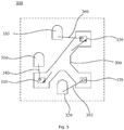
- the first sub-pixel 110, the second sub-pixel 120, and the third sub-pixel 130 are of face-up structure, the first sub-pixel 110, the second sub-pixel 120, and the third sub-pixel 130 are fixed to a common electrode 300 with a chip bonding adhesive, a first bonding wire area 310, a second bonding wire area 320 and a third bonding wire area 330 are all spaced apart from the common electrode 300, the first sub-pixel 110 is electrically connected to the first bonding wire area 310 through a first bonding wire 340, the second sub-pixel 120 is electrically connected to the second bonding wire area 320 through a second bonding wire 350, and the third sub-pixel 130 is electrically connected to the third bonding wire area 330 through a third bonding wire 360. Therefore, the bonding wire areas are spaced part from the chip bonding adhesive, so that the quality of the bonding wires is guaranteed.
- the first chip 111, the second chip 112, and the third chip 113 are of face-up structure, two first chips 111 are fixed to a common electrode 121 by a chip bonding adhesive, a first bonding wire area 122 is provided between the first chip 111 and the third chip 113, a second bonding wire area 123 is provided between the other first chip 111 and the second chip 112, the two first chips 111 are independently connected to the first bonding wire area 122 and the second bonding wire area 123 through bonding wires 124, and the second chip 112 and the third chip 113 are both connected to the common electrode 121 through bonding wires 124.
- first bonding wire area 122 and the second bonding wire area 123 are located on both sides of the chip bonding adhesive, so that the bonding wire areas are spaced apart from the chip bonding adhesive, which is beneficial to ensure the quality of bonding wires.
- an embodiment also relates to a display device comprising the display panel as described above.
- the display device may be a digital device such as a display screen, a cell phone, a tablet, a palmtop computer, a smart watch, etc.
Landscapes
- Engineering & Computer Science (AREA)
- Physics & Mathematics (AREA)
- General Physics & Mathematics (AREA)
- Theoretical Computer Science (AREA)
- Computer Hardware Design (AREA)
- Devices For Indicating Variable Information By Combining Individual Elements (AREA)
- Electroluminescent Light Sources (AREA)
- Control Of Indicators Other Than Cathode Ray Tubes (AREA)
- Control Of El Displays (AREA)
- Chemical & Material Sciences (AREA)
- Crystallography & Structural Chemistry (AREA)
- Nonlinear Science (AREA)
- Mathematical Physics (AREA)
- Optics & Photonics (AREA)
- Liquid Crystal (AREA)
Applications Claiming Priority (3)
| Application Number | Priority Date | Filing Date | Title |
|---|---|---|---|
| CN201921207314.3U CN210142481U (zh) | 2019-07-26 | 2019-07-26 | 像素结构、显示面板及显示装置 |
| CN202021141796.XU CN212209487U (zh) | 2020-06-18 | 2020-06-18 | 显示面板及显示装置 |
| PCT/CN2020/103670 WO2021017992A1 (fr) | 2019-07-26 | 2020-07-23 | Structure de pixels, panneau d'affichage et appareil d'affichage |
Publications (2)
| Publication Number | Publication Date |
|---|---|
| EP3893232A1 true EP3893232A1 (fr) | 2021-10-13 |
| EP3893232A4 EP3893232A4 (fr) | 2022-03-30 |
Family
ID=74229425
Family Applications (1)
| Application Number | Title | Priority Date | Filing Date |
|---|---|---|---|
| EP20846067.5A Pending EP3893232A4 (fr) | 2019-07-26 | 2020-07-23 | Structure de pixels, panneau d'affichage et appareil d'affichage |
Country Status (8)
| Country | Link |
|---|---|
| US (1) | US12514050B2 (fr) |
| EP (1) | EP3893232A4 (fr) |
| JP (1) | JP7281549B2 (fr) |
| KR (2) | KR20210099058A (fr) |
| AU (1) | AU2020323022B2 (fr) |
| CA (1) | CA3125304C (fr) |
| DE (1) | DE202020006122U1 (fr) |
| WO (1) | WO2021017992A1 (fr) |
Families Citing this family (4)
| Publication number | Priority date | Publication date | Assignee | Title |
|---|---|---|---|---|
| CN114822375A (zh) * | 2022-03-18 | 2022-07-29 | 长春希达电子技术有限公司 | 一种显示面板虚拟像素复用结构、控制方法以及系统 |
| CN115084213B (zh) * | 2022-07-29 | 2024-09-24 | 京东方科技集团股份有限公司 | 一种显示面板、显示装置 |
| CN115472652A (zh) * | 2022-08-26 | 2022-12-13 | 武汉华星光电半导体显示技术有限公司 | 显示面板 |
| CN121510753A (zh) * | 2024-09-20 | 2026-02-10 | 天马新型显示技术研究院(厦门)有限公司 | 阵列基板、像素排布结构、显示面板及显示装置 |
Family Cites Families (36)
| Publication number | Priority date | Publication date | Assignee | Title |
|---|---|---|---|---|
| JPH04113466A (ja) | 1990-09-04 | 1992-04-14 | Nec Corp | 画像ファイル検索システム |
| US7215347B2 (en) * | 1997-09-13 | 2007-05-08 | Gia Chuong Phan | Dynamic pixel resolution, brightness and contrast for displays using spatial elements |
| DE19746329A1 (de) * | 1997-09-13 | 1999-03-18 | Gia Chuong Dipl Ing Phan | Display und Verfahren zur Ansteuerung des Displays |
| JP2000200061A (ja) * | 1999-01-05 | 2000-07-18 | Nec Corp | 表示装置及びその制御方法 |
| TWI227340B (en) * | 2002-02-25 | 2005-02-01 | Himax Tech Inc | Color filter and liquid crystal display |
| US7907133B2 (en) * | 2006-04-13 | 2011-03-15 | Daktronics, Inc. | Pixel interleaving configurations for use in high definition electronic sign displays |
| JP2007147802A (ja) * | 2005-11-25 | 2007-06-14 | Epson Imaging Devices Corp | 表示装置 |
| US8026669B2 (en) * | 2006-03-31 | 2011-09-27 | Canon Kabushiki Kaisha | Display device |
| JP5403860B2 (ja) * | 2006-10-10 | 2014-01-29 | 株式会社ジャパンディスプレイ | カラー液晶表示装置 |
| JP5215090B2 (ja) * | 2008-02-25 | 2013-06-19 | 三菱電機株式会社 | 画像表示装置及び画像表示装置用表示ユニット |
| CA2686174A1 (fr) * | 2009-12-01 | 2011-06-01 | Ignis Innovation Inc | Architecture de pixels haute resolution |
| WO2011092944A1 (fr) * | 2010-01-28 | 2011-08-04 | シャープ株式会社 | Dispositif d'affichage couleur multiprimaire |
| JP5368590B2 (ja) * | 2010-01-29 | 2013-12-18 | シャープ株式会社 | 液晶表示装置 |
| JP5694026B2 (ja) * | 2011-03-25 | 2015-04-01 | 株式会社ジャパンディスプレイ | 表示装置 |
| KR101615332B1 (ko) * | 2012-03-06 | 2016-04-26 | 삼성디스플레이 주식회사 | 유기 발광 표시 장치의 화소 배열 구조 |
| JP2014074752A (ja) * | 2012-10-03 | 2014-04-24 | Sony Corp | 画像表示装置および画像表示装置の駆動方法、並びに、信号生成装置、信号生成プログラムおよび信号生成方法 |
| US20150016104A1 (en) | 2013-07-11 | 2015-01-15 | Everlight Electronics Co., Ltd. | Lighting Component And Lighting Device |
| JP2015019068A (ja) * | 2013-07-11 | 2015-01-29 | 億光電子工業股▲ふん▼有限公司Everlight Electronics Co.,Ltd. | 発光部材及び照明装置 |
| CN204029292U (zh) * | 2014-04-08 | 2014-12-17 | 深圳市奥蕾达科技有限公司 | 一种晶片分散邦定像素复用led模组 |
| TWI556478B (zh) * | 2014-06-30 | 2016-11-01 | 億光電子工業股份有限公司 | 發光二極體裝置 |
| WO2016008158A1 (fr) * | 2014-07-18 | 2016-01-21 | 深圳市奥拓电子股份有限公司 | Structure d'agencement virtuel a diodes electroluminescentes et ecran d'affichage a diodes electroluminescentes comportant une telle structure |
| US9342865B2 (en) * | 2014-09-25 | 2016-05-17 | Sony Corporation | Sigma-delta ADC with integrated raw image scaling filter |
| CN104375302B (zh) * | 2014-10-27 | 2020-09-08 | 上海中航光电子有限公司 | 一种像素结构、显示面板及其像素补偿方法 |
| JP2017037179A (ja) * | 2015-08-10 | 2017-02-16 | 株式会社ジャパンディスプレイ | 表示装置及びその駆動方法 |
| US10573667B2 (en) * | 2015-12-11 | 2020-02-25 | Semiconductor Energy Laboratory Co., Ltd. | Display device |
| CN205881361U (zh) * | 2016-05-22 | 2017-01-11 | 上海大学 | 一种led显示屏 |
| CN206021812U (zh) | 2016-05-28 | 2017-03-15 | 上海大学 | 一种led显示屏 |
| CN206076230U (zh) * | 2016-09-23 | 2017-04-05 | 利亚德光电股份有限公司 | Led显示装置 |
| CN106298753B (zh) * | 2016-09-23 | 2019-05-17 | 利亚德光电股份有限公司 | Led显示装置 |
| CN107256921A (zh) | 2017-05-27 | 2017-10-17 | 深圳雷曼光电科技股份有限公司 | Cob‑led封装方法、显示装置和照明装置 |
| CN107146838B (zh) | 2017-07-05 | 2019-02-26 | 深圳市彩立德照明光电科技有限公司 | 一种led器件的封装工艺及led器件 |
| CN109903684A (zh) * | 2017-12-08 | 2019-06-18 | 郑州希硕信息科技有限公司 | Led结构及其led屏 |
| DE102017129981B4 (de) * | 2017-12-14 | 2025-12-04 | OSRAM Opto Semiconductors Gesellschaft mit beschränkter Haftung | Anzeigevorrichtung |
| CN108231845B (zh) * | 2018-01-02 | 2020-04-24 | 上海天马有机发光显示技术有限公司 | 一种显示面板、电子设备 |
| CN210142481U (zh) * | 2019-07-26 | 2020-03-13 | 深圳雷曼光电科技股份有限公司 | 像素结构、显示面板及显示装置 |
| US20210360154A1 (en) * | 2020-05-14 | 2021-11-18 | David Elliott Slobodin | Display and image-capture device |
-
2020
- 2020-07-23 JP JP2021538834A patent/JP7281549B2/ja active Active
- 2020-07-23 KR KR1020217020274A patent/KR20210099058A/ko not_active Ceased
- 2020-07-23 CA CA3125304A patent/CA3125304C/fr active Active
- 2020-07-23 DE DE202020006122.0U patent/DE202020006122U1/de active Active
- 2020-07-23 WO PCT/CN2020/103670 patent/WO2021017992A1/fr not_active Ceased
- 2020-07-23 EP EP20846067.5A patent/EP3893232A4/fr active Pending
- 2020-07-23 AU AU2020323022A patent/AU2020323022B2/en active Active
- 2020-07-23 KR KR1020237033641A patent/KR20230143630A/ko not_active Ceased
-
2021
- 2021-06-29 US US17/362,837 patent/US12514050B2/en active Active
Also Published As
| Publication number | Publication date |
|---|---|
| AU2020323022A1 (en) | 2021-07-15 |
| JP2022516299A (ja) | 2022-02-25 |
| WO2021017992A1 (fr) | 2021-02-04 |
| DE202020006122U1 (de) | 2025-06-30 |
| CA3125304A1 (fr) | 2021-02-04 |
| US20210327959A1 (en) | 2021-10-21 |
| AU2020323022B2 (en) | 2023-02-02 |
| CA3125304C (fr) | 2023-08-15 |
| KR20210099058A (ko) | 2021-08-11 |
| KR20230143630A (ko) | 2023-10-12 |
| JP7281549B2 (ja) | 2023-05-25 |
| EP3893232A4 (fr) | 2022-03-30 |
| US12514050B2 (en) | 2025-12-30 |
Similar Documents
| Publication | Publication Date | Title |
|---|---|---|
| US12514050B2 (en) | Pixel structure, display panel, and display device | |
| EP3882975B1 (fr) | Substrat matriciel d'oled, panneau d'affichage et dispositif d'affichage | |
| US10923537B2 (en) | Display screens and display devices | |
| US8711067B2 (en) | Pixel interleaving configurations for use in high definition electronic sign displays | |
| CN110119031B (zh) | 立体显示装置以及空中立体显示装置 | |
| US4851824A (en) | Light emitting diode display panel | |
| EP1473772A3 (fr) | Dispositif d'affichage couleur à diodes électroluminescentes organiques à efficacité de puissance améliorée | |
| CN113380190A (zh) | 显示面板和显示设备 | |
| US12315846B2 (en) | Electronic device having two groups of light-emitting units | |
| US20220157897A1 (en) | Pixel arrangement structure and display panel | |
| JP2009048791A (ja) | バックライト及び表示装置 | |
| CN212209488U (zh) | 像素结构、显示面板及显示装置 | |
| CN111164758A (zh) | 一种改善边缘色偏的显示装置及电视机 | |
| EP4131416A1 (fr) | Substrat de réseau et appareil d'affichage | |
| US20160274416A1 (en) | Liquid crystal display module and liquid crystal display device | |
| CN210142481U (zh) | 像素结构、显示面板及显示装置 | |
| CN212209487U (zh) | 显示面板及显示装置 | |
| TW201238395A (en) | Color LED display device without color separation | |
| CN115311955B (zh) | 一种基于多合一器件的无偏色led显示屏 | |
| US20260107654A1 (en) | Display panel and display device | |
| CN119516905A (zh) | 微型发光二极管的显示器 | |
| CN223810106U (zh) | 显示面板及显示装置 | |
| CN111383551A (zh) | 一种led灯珠及led显示屏 | |
| US10453382B2 (en) | Light emitting apparatus, display section, and controller circuit | |
| CN213182255U (zh) | 一种背光光源、显示屏和电子产品 |
Legal Events
| Date | Code | Title | Description |
|---|---|---|---|
| STAA | Information on the status of an ep patent application or granted ep patent |
Free format text: STATUS: THE INTERNATIONAL PUBLICATION HAS BEEN MADE |
|
| PUAI | Public reference made under article 153(3) epc to a published international application that has entered the european phase |
Free format text: ORIGINAL CODE: 0009012 |
|
| STAA | Information on the status of an ep patent application or granted ep patent |
Free format text: STATUS: REQUEST FOR EXAMINATION WAS MADE |
|
| 17P | Request for examination filed |
Effective date: 20210628 |
|
| AK | Designated contracting states |
Kind code of ref document: A1 Designated state(s): AL AT BE BG CH CY CZ DE DK EE ES FI FR GB GR HR HU IE IS IT LI LT LU LV MC MK MT NL NO PL PT RO RS SE SI SK SM TR |
|
| A4 | Supplementary search report drawn up and despatched |
Effective date: 20220302 |
|
| RIC1 | Information provided on ipc code assigned before grant |
Ipc: G02F 1/1345 20060101ALI20220224BHEP Ipc: G09F 9/30 20060101AFI20220224BHEP |
|
| DAV | Request for validation of the european patent (deleted) | ||
| DAX | Request for extension of the european patent (deleted) | ||
| STAA | Information on the status of an ep patent application or granted ep patent |
Free format text: STATUS: EXAMINATION IS IN PROGRESS |
|
| 17Q | First examination report despatched |
Effective date: 20240212 |