EP4565039A1 - Optoelektronische vorrichtung mit drei-elektroden-dioden und verfahren zu deren herstellung - Google Patents
Optoelektronische vorrichtung mit drei-elektroden-dioden und verfahren zu deren herstellung Download PDFInfo
- Publication number
- EP4565039A1 EP4565039A1 EP24215623.0A EP24215623A EP4565039A1 EP 4565039 A1 EP4565039 A1 EP 4565039A1 EP 24215623 A EP24215623 A EP 24215623A EP 4565039 A1 EP4565039 A1 EP 4565039A1
- Authority
- EP
- European Patent Office
- Prior art keywords
- electrically conductive
- layer
- electrodes
- diodes
- electrically
- Prior art date
- Legal status (The legal status is an assumption and is not a legal conclusion. Google has not performed a legal analysis and makes no representation as to the accuracy of the status listed.)
- Pending
Links
Images




Classifications
-
- H—ELECTRICITY
- H10—SEMICONDUCTOR DEVICES; ELECTRIC SOLID-STATE DEVICES NOT OTHERWISE PROVIDED FOR
- H10H—INORGANIC LIGHT-EMITTING SEMICONDUCTOR DEVICES HAVING POTENTIAL BARRIERS
- H10H20/00—Individual inorganic light-emitting semiconductor devices having potential barriers, e.g. light-emitting diodes [LED]
- H10H20/80—Constructional details
- H10H20/83—Electrodes
- H10H20/831—Electrodes characterised by their shape
- H10H20/8312—Electrodes characterised by their shape extending at least partially through the bodies
-
- H—ELECTRICITY
- H10—SEMICONDUCTOR DEVICES; ELECTRIC SOLID-STATE DEVICES NOT OTHERWISE PROVIDED FOR
- H10W—GENERIC PACKAGES, INTERCONNECTIONS, CONNECTORS OR OTHER CONSTRUCTIONAL DETAILS OF DEVICES COVERED BY CLASS H10
- H10W90/00—Package configurations
-
- H—ELECTRICITY
- H10—SEMICONDUCTOR DEVICES; ELECTRIC SOLID-STATE DEVICES NOT OTHERWISE PROVIDED FOR
- H10F—INORGANIC SEMICONDUCTOR DEVICES SENSITIVE TO INFRARED RADIATION, LIGHT, ELECTROMAGNETIC RADIATION OF SHORTER WAVELENGTH OR CORPUSCULAR RADIATION
- H10F77/00—Constructional details of devices covered by this subclass
- H10F77/20—Electrodes
- H10F77/206—Electrodes for devices having potential barriers
-
- H—ELECTRICITY
- H10—SEMICONDUCTOR DEVICES; ELECTRIC SOLID-STATE DEVICES NOT OTHERWISE PROVIDED FOR
- H10F—INORGANIC SEMICONDUCTOR DEVICES SENSITIVE TO INFRARED RADIATION, LIGHT, ELECTROMAGNETIC RADIATION OF SHORTER WAVELENGTH OR CORPUSCULAR RADIATION
- H10F77/00—Constructional details of devices covered by this subclass
- H10F77/20—Electrodes
- H10F77/244—Electrodes made of transparent conductive layers, e.g. transparent conductive oxide [TCO] layers
-
- H—ELECTRICITY
- H10—SEMICONDUCTOR DEVICES; ELECTRIC SOLID-STATE DEVICES NOT OTHERWISE PROVIDED FOR
- H10F—INORGANIC SEMICONDUCTOR DEVICES SENSITIVE TO INFRARED RADIATION, LIGHT, ELECTROMAGNETIC RADIATION OF SHORTER WAVELENGTH OR CORPUSCULAR RADIATION
- H10F77/00—Constructional details of devices covered by this subclass
- H10F77/30—Coatings
- H10F77/306—Coatings for devices having potential barriers
-
- H—ELECTRICITY
- H10—SEMICONDUCTOR DEVICES; ELECTRIC SOLID-STATE DEVICES NOT OTHERWISE PROVIDED FOR
- H10H—INORGANIC LIGHT-EMITTING SEMICONDUCTOR DEVICES HAVING POTENTIAL BARRIERS
- H10H20/00—Individual inorganic light-emitting semiconductor devices having potential barriers, e.g. light-emitting diodes [LED]
- H10H20/01—Manufacture or treatment
- H10H20/011—Manufacture or treatment of bodies, e.g. forming semiconductor layers
- H10H20/018—Bonding of wafers
-
- H—ELECTRICITY
- H10—SEMICONDUCTOR DEVICES; ELECTRIC SOLID-STATE DEVICES NOT OTHERWISE PROVIDED FOR
- H10H—INORGANIC LIGHT-EMITTING SEMICONDUCTOR DEVICES HAVING POTENTIAL BARRIERS
- H10H20/00—Individual inorganic light-emitting semiconductor devices having potential barriers, e.g. light-emitting diodes [LED]
- H10H20/062—Light-emitting semiconductor devices having field effect type light-emitting regions, e.g. light-emitting High-Electron Mobility Transistors
-
- H—ELECTRICITY
- H10—SEMICONDUCTOR DEVICES; ELECTRIC SOLID-STATE DEVICES NOT OTHERWISE PROVIDED FOR
- H10H—INORGANIC LIGHT-EMITTING SEMICONDUCTOR DEVICES HAVING POTENTIAL BARRIERS
- H10H20/00—Individual inorganic light-emitting semiconductor devices having potential barriers, e.g. light-emitting diodes [LED]
- H10H20/80—Constructional details
- H10H20/83—Electrodes
- H10H20/831—Electrodes characterised by their shape
- H10H20/8314—Electrodes characterised by their shape extending at least partially onto an outer side surface of the bodies
-
- H—ELECTRICITY
- H10—SEMICONDUCTOR DEVICES; ELECTRIC SOLID-STATE DEVICES NOT OTHERWISE PROVIDED FOR
- H10H—INORGANIC LIGHT-EMITTING SEMICONDUCTOR DEVICES HAVING POTENTIAL BARRIERS
- H10H20/00—Individual inorganic light-emitting semiconductor devices having potential barriers, e.g. light-emitting diodes [LED]
- H10H20/80—Constructional details
- H10H20/83—Electrodes
- H10H20/832—Electrodes characterised by their material
- H10H20/833—Transparent materials
-
- H—ELECTRICITY
- H10—SEMICONDUCTOR DEVICES; ELECTRIC SOLID-STATE DEVICES NOT OTHERWISE PROVIDED FOR
- H10H—INORGANIC LIGHT-EMITTING SEMICONDUCTOR DEVICES HAVING POTENTIAL BARRIERS
- H10H20/00—Individual inorganic light-emitting semiconductor devices having potential barriers, e.g. light-emitting diodes [LED]
- H10H20/80—Constructional details
- H10H20/84—Coatings, e.g. passivation layers or antireflective coatings
-
- H—ELECTRICITY
- H10—SEMICONDUCTOR DEVICES; ELECTRIC SOLID-STATE DEVICES NOT OTHERWISE PROVIDED FOR
- H10H—INORGANIC LIGHT-EMITTING SEMICONDUCTOR DEVICES HAVING POTENTIAL BARRIERS
- H10H29/00—Integrated devices, or assemblies of multiple devices, comprising at least one light-emitting semiconductor element covered by group H10H20/00
- H10H29/01—Manufacture or treatment
- H10H29/036—Manufacture or treatment of packages
- H10H29/0364—Manufacture or treatment of packages of interconnections
-
- H—ELECTRICITY
- H10—SEMICONDUCTOR DEVICES; ELECTRIC SOLID-STATE DEVICES NOT OTHERWISE PROVIDED FOR
- H10H—INORGANIC LIGHT-EMITTING SEMICONDUCTOR DEVICES HAVING POTENTIAL BARRIERS
- H10H29/00—Integrated devices, or assemblies of multiple devices, comprising at least one light-emitting semiconductor element covered by group H10H20/00
- H10H29/10—Integrated devices comprising at least one light-emitting semiconductor component covered by group H10H20/00
- H10H29/14—Integrated devices comprising at least one light-emitting semiconductor component covered by group H10H20/00 comprising multiple light-emitting semiconductor components
- H10H29/142—Two-dimensional arrangements, e.g. asymmetric LED layout
-
- H—ELECTRICITY
- H10—SEMICONDUCTOR DEVICES; ELECTRIC SOLID-STATE DEVICES NOT OTHERWISE PROVIDED FOR
- H10H—INORGANIC LIGHT-EMITTING SEMICONDUCTOR DEVICES HAVING POTENTIAL BARRIERS
- H10H29/00—Integrated devices, or assemblies of multiple devices, comprising at least one light-emitting semiconductor element covered by group H10H20/00
- H10H29/80—Constructional details
- H10H29/832—Electrodes
- H10H29/8322—Electrodes characterised by their materials
- H10H29/8323—Transparent materials
-
- H—ELECTRICITY
- H10—SEMICONDUCTOR DEVICES; ELECTRIC SOLID-STATE DEVICES NOT OTHERWISE PROVIDED FOR
- H10H—INORGANIC LIGHT-EMITTING SEMICONDUCTOR DEVICES HAVING POTENTIAL BARRIERS
- H10H29/00—Integrated devices, or assemblies of multiple devices, comprising at least one light-emitting semiconductor element covered by group H10H20/00
- H10H29/80—Constructional details
- H10H29/842—Coatings, e.g. passivation layers or antireflective coatings
-
- H—ELECTRICITY
- H10—SEMICONDUCTOR DEVICES; ELECTRIC SOLID-STATE DEVICES NOT OTHERWISE PROVIDED FOR
- H10H—INORGANIC LIGHT-EMITTING SEMICONDUCTOR DEVICES HAVING POTENTIAL BARRIERS
- H10H29/00—Integrated devices, or assemblies of multiple devices, comprising at least one light-emitting semiconductor element covered by group H10H20/00
- H10H29/80—Constructional details
- H10H29/85—Packages
- H10H29/857—Interconnections
-
- H—ELECTRICITY
- H10—SEMICONDUCTOR DEVICES; ELECTRIC SOLID-STATE DEVICES NOT OTHERWISE PROVIDED FOR
- H10H—INORGANIC LIGHT-EMITTING SEMICONDUCTOR DEVICES HAVING POTENTIAL BARRIERS
- H10H20/00—Individual inorganic light-emitting semiconductor devices having potential barriers, e.g. light-emitting diodes [LED]
- H10H20/01—Manufacture or treatment
- H10H20/032—Manufacture or treatment of electrodes
-
- H—ELECTRICITY
- H10—SEMICONDUCTOR DEVICES; ELECTRIC SOLID-STATE DEVICES NOT OTHERWISE PROVIDED FOR
- H10H—INORGANIC LIGHT-EMITTING SEMICONDUCTOR DEVICES HAVING POTENTIAL BARRIERS
- H10H20/00—Individual inorganic light-emitting semiconductor devices having potential barriers, e.g. light-emitting diodes [LED]
- H10H20/80—Constructional details
- H10H20/81—Bodies
- H10H20/819—Bodies characterised by their shape, e.g. curved or truncated substrates
-
- H—ELECTRICITY
- H10—SEMICONDUCTOR DEVICES; ELECTRIC SOLID-STATE DEVICES NOT OTHERWISE PROVIDED FOR
- H10H—INORGANIC LIGHT-EMITTING SEMICONDUCTOR DEVICES HAVING POTENTIAL BARRIERS
- H10H20/00—Individual inorganic light-emitting semiconductor devices having potential barriers, e.g. light-emitting diodes [LED]
- H10H20/80—Constructional details
- H10H20/81—Bodies
- H10H20/822—Materials of the light-emitting regions
- H10H20/824—Materials of the light-emitting regions comprising only Group III-V materials, e.g. GaP
- H10H20/825—Materials of the light-emitting regions comprising only Group III-V materials, e.g. GaP containing nitrogen, e.g. GaN
-
- H—ELECTRICITY
- H10—SEMICONDUCTOR DEVICES; ELECTRIC SOLID-STATE DEVICES NOT OTHERWISE PROVIDED FOR
- H10H—INORGANIC LIGHT-EMITTING SEMICONDUCTOR DEVICES HAVING POTENTIAL BARRIERS
- H10H29/00—Integrated devices, or assemblies of multiple devices, comprising at least one light-emitting semiconductor element covered by group H10H20/00
- H10H29/80—Constructional details
- H10H29/832—Electrodes
- H10H29/8321—Electrodes characterised by their shape
Definitions
- This description generally relates to the field of optoelectronic devices comprising light-emitting diodes (also called “LEDs” or “LEDs” for “Light-Emitting Diode” in English) used for example for the production of any light-emitting device (screens, projectors, image walls, etc.), and/or photodiodes.
- light-emitting diodes also called “LEDs” or “LEDs” for "Light-Emitting Diode” in English
- any light-emitting device screens, projectors, image walls, etc.
- the document EP 2 960 951 A1 describes an optoelectronic device of the LED or photodiode type comprising, in addition to the two electrodes each connected to one of the semiconductors of a pn junction, a third electrode produced in the form of a grid or Schottky contact.
- This third electrode makes it possible, by generating a lateral electric field making it possible to increase the EQE (external quantum efficiency), to circumvent the problem of lack of charge carriers in certain semiconductor materials due to an excessively high activation energy of the dopants in these semiconductor materials, such as for example in materials with large gaps such as diamond or epitaxial structures based on AlGaN used in particular for LEDs emitting in the UV range.
- the third electrode of the LEDs and/or photodiodes is common and distributed for all of these LEDs and/or photodiodes, for example in the form of trenches formed around the pn junctions or through the pn junctions of the LEDs and/or photodiodes.
- a disadvantage of such an optoelectronic device is that the electrical contact of the electrodes requires very precise alignment when this device is made with small dimensions. It is possible to facilitate this contact by making the device with larger dimensions, and therefore to the detriment of the compactness of the device.
- the electrically conductive layer is interrupted at the bottom walls of the trenches.
- bottom walls of the trenches are at least partly formed by the second electrodes.
- the electrically conductive portions are electrically coupled to the portions of the second semiconductor layer of at least a portion of the diodes corresponding to LEDs.
- the electrically conductive portions are electrically coupled to the portions of the second semiconductor layer of the LEDs by at least one electrically conductive and optically transparent layer arranged on the stack and on the electrically conductive portions.
- the electrically conductive and optically transparent layer is electrically insulated from the electrically conductive layer by dielectric portions arranged between the electrically conductive layer and the electrically conductive and optically transparent layer.
- the electrically conductive portions are electrically insulated from the electrically conductive layer by at least a first dielectric layer arranged between the electrically conductive portions and the electrically conductive layer.
- the third electrode is arranged at an edge of the optoelectronic device.
- the device comprises several third electrodes each electrically coupled to one of the electrically conductive portions, each of the first electrodes being arranged between one of the second electrodes and one of the third electrodes, and each of the third electrodes is disposed between one of the first electrodes and one of the second electrodes.
- the portions of the electrically conductive layer arranged around at least a portion of the diodes corresponding to photodiodes are electrically coupled to the portions of the second semiconductor layer of the photodiodes.
- the parts of the electrically conductive layer arranged around the photodiodes are electrically coupled to the portions of the second semiconductor layer of the photodiodes by at least one electrically conductive and optically transparent layer arranged on the stack and on the parts of the electrically conductive layer arranged around the photodiodes.
- the device further comprises a second dielectric layer arranged between the electrically conductive layer and the stack.
- the expressions "about”, “approximately”, “substantially”, and “of the order of” mean to within 10%, preferably to within 5%.
- diode is used to refer to a light-emitting diode or photodiode.
- LED refers to an LED or micro-LED.
- the term "layer” is used to refer to a layer comprising a single material or multiple materials arranged against each other, i.e., a stack.
- dotted lines are shown to illustrate that the elements of the device 100 shown on either side of these dotted lines are not necessarily arranged directly next to each other.
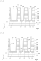
- the device 100 comprises an integrated control circuit 102 comprising at least, in a metallization level 104, first electrodes 106 and second electrodes 108.
- the circuit 102 which corresponds for example to an ASIC (“Application-specific integrated circuit” in English, or specialized integrated circuit), comprises electronic components making it possible in particular to implement different control functions. of diodes of the device 100, these functions not being detailed here.
- ASIC Application-specific integrated circuit
- FIG. 1 only level 104 is shown, although circuit 102 may comprise several levels of superimposed metallizations making the electrical connections of the electronic components of circuit 102.
- level 104 comprises a dielectric layer 110 in which the electrodes 106, 108 are arranged.
- This dielectric layer 110 comprises, for example, SiO 2 and its thickness (dimension parallel to the Z axis on the Figure 1 ) is for example equal to 1 ⁇ m.
- the first electrodes 106 correspond to anodes of the diodes of the device 100
- the second electrodes 108 correspond to electrodes to which grids surrounding the pn junctions of the diodes of the device 100 are electrically coupled.
- Figure 1 only two first electrodes 106 and two second electrodes 108 are shown.
- the total number of first and second electrodes 106, 108 of the device 100 depends in particular on the number of diodes of the device 100. Alternatively, other configurations of the first and second electrodes 106, 108 are possible.
- the circuit 102 also comprises, in the level 104, at least one third electrode 111 serving as cathode of the diodes of the device 100.
- the device 100 comprises a third electrode 111 forming a cathode common to the diodes of the device 100.
- the third electrode 111 is arranged at the periphery of the device 100, that is to say at the level of an edge of the device 100 and not within the set of diodes of the device 100.
- the electrodes 106, 108, 111 comprise, for example, a metallic material such as aluminum or copper.
- these metal layers 112, 114, 116 are used in particular for implementing, during the production of the device 100, a direct metal/metal bonding between on one side the first stack 112 and a part of the layer 114 produced on the circuit 102, and on the other side the second stack 116 and another part of the layer 114 produced on a stack of layers used for producing the diodes of the device 100.
- these metal layers could be different from those described in the example of the Figure 1 , both in terms of number of layers, thicknesses, materials, etc.
- a layer of AlSi 118 is arranged on the second stack 116, and has for example a thickness equal to 100 nm.
- the device 100 further comprises a plurality of diodes 126 each comprising a portion of a stack of at least a first and a second semiconductor layer. 120, 122 doped according to opposite conductivity types.
- the semiconductor of the first layer 120 is p-doped
- the semiconductor of the second layer 122 is n-doped.
- this semiconductor stack further comprises an active zone 124 arranged between the layers 120, 122 and comprising one or more emissive or receiving (optically absorbing) layers each forming a quantum well and each arranged between two barrier layers. All the layers of the active zone 124, i.e.
- the emissive/receiving layer(s) and the barrier layers comprise intrinsic semiconductor materials, i.e. not intentionally doped (with a concentration of residual donors n nid for example between approximately 10 15 and 10 18 donors/cm 3 ).
- the semiconductor stack is arranged, for example bonded, on the level 104 (with, in the example of the Figure 1 , layers 112 to 118 arranged between level 104 and the semiconductor stack) and here forms, for each diode 126, a pin junction.
- the first and second layers 120, 122 may comprise AlGaN and the layer(s) of the active zone 124 may comprise GaN.
- the layers 120, 122, 124 may be used for producing the layers 120, 122, 124, for example arsenide or phosphide type semiconductors.
- all the diodes 126 of the device 100 correspond to LEDs.
- two diodes 126 are shown, each comprising a portion of the stack of layers 120, 122, 124.
- a portion of the first semiconductor layer 120 of each diode 126 is electrically coupled to one of the first electrodes 106 disposed under this portion of the first semiconductor layer 120, this electrical coupling being achieved by means of an electrically conductive via 128 formed between the first electrode 106 and the portions of the metal layers 112, 114, 116 disposed on this first electrode 106 and which are in contact with this portion of the first semiconductor layer 120.
- the interface between the circuit 102 and the semiconductor stack of diodes 126, or between the level 104 and the semiconductor stack of diodes 126 is formed by layers different from the layers 112 to 118, depending in particular on the techniques implemented for the production of the device 100.
- the device 100 also comprises trenches 130 passing through the semiconductor stack (i.e., layers 120, 122 and 124), surrounding and separating the diodes 126 from each other and whose bottom walls are at less partly formed by the second electrodes 108. In the embodiment described, these trenches 130 also pass through the layers 112, 114, 116 and 118, as well as part of the dielectric layer 110 until reaching the second electrodes 108.
- the semiconductor stack i.e., layers 120, 122 and 124
- these trenches 130 also pass through the layers 112, 114, 116 and 118, as well as part of the dielectric layer 110 until reaching the second electrodes 108.
- the trenches 130 are for example made such that they form, through the different layers in which these trenches 130 are made, a grid delimiting the diodes 126 whose section, in a plane parallel to the main planes in which these different layers extend (plane parallel to the plane (X,Y) visible on the Figure 1 ), is square, hexagonal or rectangular in shape.
- the dimension of one of the trenches 130 between two adjacent diodes 126 i.e. the width of each trench 130 (which corresponds to the dimension of the trench 130 parallel to the X axis on the Figure 1 ), is for example equal to approximately 1 ⁇ m.
- another trench 131 passes through the semiconductor stack as well as the layers 112, 114, 116 and 118 and a part of the dielectric layer 110.
- this trench 131 comprises a bottom wall opening onto the third electrode 111 and allows electrical contact to be made with the third electrode 111.
- the side walls, or flanks, of the trenches 130, 131 are covered with a dielectric layer 132 serving as a passivation layer and comprising for example at least one of the following materials: alumina, AlN, SiO 2 , SiN.
- the dielectric layer 132 is covered, at the level of the side walls of the trenches 130, 131, by an electrically conductive layer 134.
- This electrically conductive layer conductive 134 is also arranged against the bottom walls of the trenches 130, 131.
- the electrically conductive layer 134 is therefore electrically insulated from the stack of layers present on the circuit 102 by the dielectric layer 132.
- the electrically conductive layer 134 is electrically coupled to the second electrodes 108 and is interrupted so that parts of this electrically conductive layer 134 arranged around each of the diodes 126 are electrically insulated from other parts of this electrically conductive layer 134 arranged around the other diodes 126.
- the electrically conductive layer 134 is interrupted at the bottom walls of the trenches 130. In the example of the Figure 1 , the electrically conductive layer 134 is not interrupted in the trench 131.
- the electrically conductive layer 134 comprises at least one metal.
- This metal can, for example, allow light reflection, in particular in the visible range, which allows the light emitted laterally by the diodes 126 to be reflected against the electrically conductive layer 134 and thus avoid disturbing the neighboring diodes 126.
- the electrically conductive layer 134 is covered by another dielectric layer 136 which also covers the parts of the dielectric layer 132 located at the interrupted parts of the electrically conductive layer 134 (at the bottom walls of the trenches 130 in the example of the Figure 1 ).
- This other dielectric layer 136 comprises, for example, SiO 2 or alumina.
- the dielectric layer 136 is interrupted at the bottom wall of the trench 131 so that the layer electrically conductive 134 is electrically accessible from the bottom of the trench 131.
- each of the electrically conductive portions 138 comprises a stack of several materials, for example a stack of Ti/TiN and copper.
- the electrically conductive portion 138 is electrically coupled to the electrically conductive layer 134, and therefore also to the third electrode 111.
- the device 100 further comprises dielectric portions 140, for example comprising SiN, extending over the tops of the portions of the electrically conductive layer 134.
- the device 100 comprises an electrically conductive and optically transparent layer 142 arranged on an upper face of the device 100 and which electrically couples the electrically conductive portions 138 to each other and to the portions of the second semiconductor layer 122 of the diodes 126.
- This layer 142 is electrically insulated from the electrically conductive layer 134 by the dielectric portions 140.
- the electrically conductive and optically transparent layer 142 may comprise a transparent conductive oxide, for example ITO, in order to allow light emission from the diodes 126 therethrough.
- the layer 142 also ensures the spreading (“spreading”) of the current over the distance between the semiconductor of the second layer 122 and the electrically conductive portions 138.
- the metallic filling of the trenches 130, 131 allows the electrical coupling between the portions of the second semiconductor layer 122 of the diodes 126 and the third electrode 111 which corresponds to the common cathode of the diodes 126.
- the device 100 also comprises a connection pad 144 arranged on the electrically conductive portion 138 arranged in the trench 131, and serving as electrical access to the common cathode of the diodes 126.
- the device 100 comprises diodes 126 that can be controlled independently of each other and can be addressed by electrical control potentials applied by the circuit 102 to the anodes corresponding to the first electrodes 106.
- the grids formed by the parts of the electrically conductive layer 134 around the semiconductor stacks of the diodes 126 can be controlled independently of each other and can be addressed by electrical control potentials applied by the circuit 102 to the second electrodes 108.
- the application of an electrical potential to these grids can modify the distribution of the carriers on the lateral sides of the P or N doped semiconductor (depending on the potential applied), which makes it possible to increase the light emission efficiency of the diodes 126. When these electrical potentials are applied to these grids, no current flows in these grids.
- the thickness of the dielectric layer 132 can be chosen such that it is sufficient to avoid breakdown when a potential electric is applied to the grids of the diodes 126, without however being too thick in order to maximize the field effect applied via the grid of the diodes 126.
- the thickness of this dielectric layer 132 is for example between 10 nm and 60 nm, depending on the dielectric characteristics of the material(s) of this layer 132.
- the thickness of the dielectric layer 136 can be chosen such that it is sufficient to avoid breakdown due to the electrical potentials applied to the gates of the diodes 126 and the reference electrical potential, for example ground, applied to the cathode.
- the dielectric layer 136 can comprise alumina and have a thickness equal to approximately 10 nm.
- the lateral flanks of the trenches 130, 131 may be perpendicular to the surface of the circuit 102 on which the semiconductor stack is secured, or form an angle such that the width of the trenches 130, 131 at the upper face of the device 100 (face at which the dielectric portions 140 and the electrically conductive and optically transparent layer 142 are present) is greater than the width of these trenches 130, 131 at the circuit 102, that is to say of the dielectric layer 110 in the example of the Figure 1
- Such a difference in width of the trenches 130, 131 can facilitate the implementation of the deposits of the materials in the trenches 130, 131.
- the device 100 described therefore comprises a compact set of diodes 126 with three electrodes, the diodes 126 of which can be controlled individually using the electrical independence of the anodes and grids of these diodes 126.
- the structure of the device 100 can allow its production by monolithic integration, directly on the circuit 102, of the junctions forming the diodes 126 without critical alignment, thanks to the fact that the singulation of the diodes 126 (corresponding to the production of the trenches 130) is carried out after the joining of the semi-conductor layers with the circuit 102.
- the integrated circuit 102 is first produced from a semiconductor substrate, for example by implementing conventional microelectronics steps (deposition, lithography, etching, etc.) to form the electronic components of this integrated circuit 102 as well as the metallization levels (BEOL) including the metallization level 104.
- the first stack 112 and a part of the layer 114 are also produced on the level 104 in anticipation of a future direct metal/metal bonding with the semiconductor stack intended for the production of the diodes 126.
- the semiconductor stack of layers 124, 122, 120 as well as layer 118, the second stack 116 and a portion of layer 114 are produced on another substrate (not shown).
- Layers 124, 122 and 120 are for example produced by epitaxy.
- One or more buffer layers may be present on this other substrate to facilitate the growth of layers 124, 122, and 120.
- a direct metal/metal bond can then be used to join the two parts of the layer 114 with each other, then the substrate used for the growth of layers 124, 122 and 120 can be removed. Any buffer layer(s) interposed between the substrate and layer 124 can also be removed, for example by thinning and etching.
- a dielectric hard mask 146 is then produced, for example by deposition, on the semiconductor layer 122.
- the dielectric hard mask 146 may comprise SiO 2 and/or SiN.
- the thickness of the dielectric hard mask 146 is here chosen such that it is sufficient to be able to etch the trenches 130, 131 until reaching the electrodes 106, 108, 111.
- the structure obtained at this stage of the method is shown in the Figure 2 .
- the trenches 130, 131 are then made through the semiconductor stack up to the electrodes 111, 106 and 108.
- lithography and etching can then be implemented, using the dielectric hard mask 146, to form the trenches 130, 131 through the layers present on the electrodes 106, 108 and 111.
- the etching implemented can judiciously use a stop layer comprising for example TiN and/or SiN and present on the metal level of the electrodes 106, 108, 111. The use of such a stop layer allows that possible variations in thickness of the etched materials do not impact the final depth of the trenches 130, 131.
- the dielectric layer 132 is then deposited in the trenches 130, 131 by covering the side walls and the bottom walls of these trenches 130, 131, and also on the dielectric hard mask 146.
- Anisotropic etching can then be implemented in order to remove the parts of the dielectric layer 132 arranged on the bottom walls of the trenches 130, 131 as well as those resting on the dielectric hard mask 146.
- the remaining portions of the dielectric layer 132 form dielectric spacers covering the flanks, or side walls, of the diodes 126.
- the structure obtained at this stage of the process is shown in FIG. Figure 4 .
- the electrically conductive layer 134 is then deposited on the structure produced, thus covering the bottom walls of the trenches 130, 131, the dielectric hard mask 146 as well as the remaining portions of the dielectric layer 132 arranged against the side walls of the trenches 130, 131.
- the electrically conductive layer 134 is in electrical contact with the second electrodes 108, that is to say those intended to form the gates of the diodes 126 in the example described.
- one or more steps of preparation of the surfaces on which the electrically conductive layer 134 is intended to be deposited can be implemented, for example to remove any native metal oxide present on these surfaces.
- the structure obtained at this stage of the process is shown in FIG. Figure 5 .
- a localized etching step can then be implemented in order to remove certain portions of the electrically conductive layer 134 such that parts of the electrically conductive layer 134 arranged around each of the diodes 126 are electrically isolated from other parts of the electrically conductive layer 134 arranged around the other diodes 126.
- this etching can be implemented such that the remaining parts of the electrically conductive layer 134 are electrically isolated from one pixel to another while maintaining electrical contact, for the remaining parts of the layer 134, around each diode 126, with one of the second electrodes 108.
- the etched parts of the electrically conductive layer 134 are located on the bottom walls of the trenches 130.
- this etching is implemented in such a way that the parts of the electrically conductive layer 134 located in the trench 131 are not etched and that the electrical contact with the third electrode 111 is maintained.
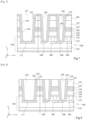
- the structure obtained at this stage of the process is shown in the Figure 6 .
- the dielectric layer 136 is then deposited on the electrically conductive layer 134, and also on the parts of the bottom walls of the trenches 130 which are no longer covered by the electrically conductive layer 134 (i.e. at the locations of the etched parts 135).
- a localized etching can then be implemented in order to remove the part of the dielectric layer 136 covering the bottom wall of the trench 131 so that the electrically conductive layer 134 remains accessible. electrically from the bottom of trench 131.
- the structure obtained at this stage of the process is shown in the Figure 7 .
- the electrically conductive portions 138 are then produced so that they fill the remaining volume of the trenches 130, 131 not occupied by the other layers previously deposited.
- the production of the portions 138 may comprise the deposition of Ti/TiN/Cu layers from which electrochemical growth of copper is then carried out.
- a planarization of the upper face of the structure produced can then be implemented, with a stop on the second semiconducting layer 122.
- This chemical-mechanical polishing makes it possible to remove the dielectric hard mask 146 as well as the parts of the layers 134 and 136 and the portions 138 arranged at the level of the dielectric hard mask 146.
- the structure obtained at this stage of the process is shown on the figure 8 .
- a dielectric encapsulation layer 140 is then deposited on the upper face of the structure produced, this layer 140 then being etched locally in order to remove the parts of this layer covering the electrically conductive portions 138 and the second semi-conductive layer 122. The remaining parts of this encapsulation layer form the dielectric portions 140.
- the electrically conductive and optically transparent layer 142 is then deposited on the upper face of the structure produced, thus making the electrical contacts between the parts of the second semi-conductive layer 122 of the diodes 126 and the electrically conductive portions 138, and also with the electrically conductive portion 138 which is in contact with the third electrode 111 corresponding to the common cathode of the diodes 126.
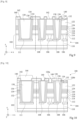
- the structure obtained at this stage of the process is shown in the Figure 9 .
- the device 100 can then be completed by implementing an electrical/chemical passivation deposit and by producing connection pads, including the connection pad 144 serving as a contact to the common cathode of the device 100.
- the device 100 obtained corresponds to that shown in the Figure 1 .
- other connection pads coupled to the anodes and/or the second electrodes 128 can also be made via routing in the metallization levels of the circuit.
- the diodes 126 of the device correspond to LEDs.
- the active zone 124 may comprise one or more receiving layers, i.e. optically absorbent layers.
- the device 100 comprises certain diodes 126 corresponding to LEDs and other diodes 126 corresponding to photodiodes.
- the diode designated by the reference 126a corresponds to an LED and is similar to the diodes 126 of the device 100 according to the first embodiment previously described.
- the part of the second semiconductor layer 122 of this diode 126a is electrically coupled to one of the electrically conductive portions 138 adjacent to this part of the second semiconductor layer 122 so that it is coupled to the common cathode of the LEDs of the device 100.
- an electrical potential different from the electrical potentials applied to the anode and the cathode of this diode 126a is intended to be applied to the gate of this diode 126a formed by the parts of the electrically conductive layer 134 arranged around the semiconductor stack of this diode 126a.
- the diode designated by the reference 126b corresponds to a photodiode which is distinguished from the diode 126a by the fact that the electrical potential intended to be applied to the part of the second semiconductor layer 122 of this photodiode 126b does not correspond to that of the common cathode but to that intended to be applied to the gate of this diode 126b formed by the parts of the electrically conductive layer 134 arranged around the semiconductor stack of this diode 126b.
- This configuration of the diode 126b is obtained thanks to the fact that the dielectric portion 140 formed next to this diode 126b covers the electrically conductive portion 138 and not one of the parts of the electrically conductive layer 134 arranged around the semiconductor stack of this diode 126b.
- the portion of the electrically conductive and optically transparent layer 142 formed above this diode 126b electrically couples the portion of the second semiconductor layer 122 of this diode 126b to one of the portions of the electrically conductive layer 134 arranged around the semiconductor stack of this diode 126b.
- the electrically conductive layer 142 is not continuous but is interrupted (interruption designated by the reference 148 on the Figure 10 ) so that the parts of layer 134 providing electrical connections for the diodes corresponding to LEDs are not electrically connected to those providing electrical connections for the diodes corresponding to photodiodes.
- the electrically conductive and optically transparent layer 142 makes it possible to differentiate the electrical potential applied to the parts of the second semiconductor layer 122 according to the nature of the diodes 126.
- the circuit 102 does not have to provide opposite voltages to the LEDs and the photodiodes of the device 100, given that the same voltage can be used for the polarization of the LEDs and the photodiodes.
- the device 100 may comprise a matrix of pixels such that each pixel of the matrix comprises a first diode similar to the diode 126a and corresponding to an LED, and a second diode similar to the diode 126b and corresponding to a photodiode.
- Each pixel of such a matrix therefore fulfills both a light emission function and a light reception function.
- the dielectric encapsulation layer is then deposited on the upper face of the structure produced. This layer is then etched locally, for example via photolithography, in order to remove, at the diodes 126a intended to form LEDs, the parts of this layer covering the electrically conductive portions 138 and the dielectric hard mask 146, and to remove, at the diodes 126b intended to form photodiodes, the parts of this layer covering the parts of the electrically conductive layer 134 and the dielectric hard mask 146.
- a sufficiently large thickness of the dielectric layer 136 facilitates the implementation of this etching so as to etch the parts of the encapsulation layer located on the parts of the electrically conductive layer and preserve those located on the electrically conductive portions 138.
- the remaining parts of this encapsulation layer form the portions dielectrics 140.
- the structure obtained at this stage of the process is visible on the Figure 12 .
- a second photolithography and etching step is then implemented to form openings 149 through the dielectric hard mask 146 allowing access to the parts of the second semiconductor layer 122 of the diodes 126a and 126b.
- the structure obtained at this stage of the process is shown in the Figure 13 .
- the electrically conductive and optically transparent layer 142 is then deposited on the upper face of the structure produced, thus making the electrical contacts between the parts of the second semi-conductive layer 122 and the electrically conductive portions 138 for the diodes 126a corresponding to LEDs, and the electrical contacts between the parts of the second semiconductor layer 122 and the parts of the electrically conductive layer 134 for the diodes 126b corresponding to photodiodes. Steps of photolithography and etching of the electrically conductive layer 142 can then be implemented so that the electrically conductive layer 142 is interrupted so that the parts of this layer 142 providing electrical connections for the diodes corresponding to LEDs are not electrically connected to those providing electrical connections for the diodes corresponding to photodiodes.
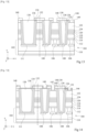
- the structure obtained at this stage of the method is shown in figure 14 .
- the device 100 can be completed as previously described for the first embodiment, the device 100 obtained corresponding to that shown in the Figure 10 .
- the third electrode 111 forms a cathode common to all of the diodes 126 corresponding to LEDs.
- the third electrode 111 is arranged at an edge of the device 100, for example next to the diode matrix 126.
- each first electrode 106 can be arranged between two second electrodes 108 to which the parts of the electrically conductive layer 134 located around the diode 126 are electrically coupled, the portion of the first semi-conductive layer 120 of which is electrically coupled to said first electrode 106.
- the device 100 can comprise several third electrodes 111 arranged in the metallization level 104, each of the third electrodes 111 being electrically coupled to one of the electrically conductive portions 138 and arranged between two second electrodes 108 each electrically coupled to parts of the electrically conductive layer 134 located around different diodes 126.
- FIG. 15 An example of a part of a device 100 according to such a variant applied here to the device 100 according to the first embodiment is shown in the Figure 15 .
- the parts of the electrically conductive layer 134 and of the dielectric layer 136 located on the bottom walls of the trenches 130 and covering the third electrodes 111 are etched so that the electrically conductive portions 138 are in electrical contact with the third electrodes 111.
- the parts of the electrically conductive layer 134 arranged in the same trench are electrically coupled to second electrodes 108 different from each other.
- This first variant can facilitate the production of the device 100, with however as a counterpart a lesser compactness of the device 100 thus produced compared to a device 100 comprising a single third electrode 111 located at the edge of the device 100.
- the device 100 in a second variant that can be applied to the first or second embodiment previously described, it is possible for the device 100 to comprise several third electrodes 111, each electrically coupled to one of the electrically conductive portions 138 and arranged in the metallization level 104, each of the first electrodes 106 being arranged between one of the second electrodes 108 and one of the third electrodes 111, and each of the third electrodes 111 is arranged between one of the first electrodes 106 and one of the second electrodes 108.
- FIG. 16 An example of such a second variant applied here to the device 100 according to the first embodiment is shown in the figure 16 .
- the electrically conductive layer 134 and the dielectric layer 136 are etched such that one of the portions of the electrically conductive layer 134 is in electrical contact with the second electrode 108 located at the bottom of the trench 130 and the electrically conductive portion 138 is in contact with the third electrode 111 located at the bottom of the trench 130.
- a portion of the electrically conductive layer 134 may be retained on the third electrode 111, the electrically conductive portion 134 being electrically coupled to the third electrode 111. Alternatively, this portion of the electrically conductive layer 134 may be removed.
- this second variant makes it easier to produce the device 100, with the drawback, however, of being less compact than when the device 100 comprises a single third electrode 111 located at the edge of the device 100.
Landscapes
- Electrodes Of Semiconductors (AREA)
- Led Devices (AREA)
Applications Claiming Priority (1)
| Application Number | Priority Date | Filing Date | Title |
|---|---|---|---|
| FR2313439A FR3156240B1 (fr) | 2023-12-01 | 2023-12-01 | Dispositif optoélectronique comprenant des diodes à trois électrodes |
Publications (1)
| Publication Number | Publication Date |
|---|---|
| EP4565039A1 true EP4565039A1 (de) | 2025-06-04 |
Family
ID=90362898
Family Applications (1)
| Application Number | Title | Priority Date | Filing Date |
|---|---|---|---|
| EP24215623.0A Pending EP4565039A1 (de) | 2023-12-01 | 2024-11-27 | Optoelektronische vorrichtung mit drei-elektroden-dioden und verfahren zu deren herstellung |
Country Status (4)
| Country | Link |
|---|---|
| US (1) | US20250185422A1 (de) |
| EP (1) | EP4565039A1 (de) |
| CN (1) | CN120091682A (de) |
| FR (1) | FR3156240B1 (de) |
Citations (4)
| Publication number | Priority date | Publication date | Assignee | Title |
|---|---|---|---|---|
| EP2960951A1 (de) | 2014-06-27 | 2015-12-30 | Commissariat à l'Énergie Atomique et aux Énergies Alternatives | Optoelektronische vorrichtung mit p-n-übergang, die eine ionisierung der dotierungsmittel durch feldeffekt ermöglicht |
| WO2019141948A1 (fr) | 2018-01-19 | 2019-07-25 | Commissariat A L'energie Atomique Et Aux Energies Alternatives | Dispositif optoélectronique comportant une grille et une cathode couplées l'une a l'autre |
| US20200052151A1 (en) * | 2018-08-10 | 2020-02-13 | Samsung Electronics Co., Ltd. | Flip-chip light emitting diode, manufacturing method of flip-chip light emitting diode and display device including flip-chip light emitting diode |
| US20220320367A1 (en) * | 2019-05-21 | 2022-10-06 | Aledia | Optoelectronic device comprising light-emitting diodes |
-
2023
- 2023-12-01 FR FR2313439A patent/FR3156240B1/fr active Active
-
2024
- 2024-11-21 US US18/954,803 patent/US20250185422A1/en active Pending
- 2024-11-26 CN CN202411697667.1A patent/CN120091682A/zh active Pending
- 2024-11-27 EP EP24215623.0A patent/EP4565039A1/de active Pending
Patent Citations (4)
| Publication number | Priority date | Publication date | Assignee | Title |
|---|---|---|---|---|
| EP2960951A1 (de) | 2014-06-27 | 2015-12-30 | Commissariat à l'Énergie Atomique et aux Énergies Alternatives | Optoelektronische vorrichtung mit p-n-übergang, die eine ionisierung der dotierungsmittel durch feldeffekt ermöglicht |
| WO2019141948A1 (fr) | 2018-01-19 | 2019-07-25 | Commissariat A L'energie Atomique Et Aux Energies Alternatives | Dispositif optoélectronique comportant une grille et une cathode couplées l'une a l'autre |
| US20200052151A1 (en) * | 2018-08-10 | 2020-02-13 | Samsung Electronics Co., Ltd. | Flip-chip light emitting diode, manufacturing method of flip-chip light emitting diode and display device including flip-chip light emitting diode |
| US20220320367A1 (en) * | 2019-05-21 | 2022-10-06 | Aledia | Optoelectronic device comprising light-emitting diodes |
Also Published As
| Publication number | Publication date |
|---|---|
| FR3156240B1 (fr) | 2026-04-24 |
| US20250185422A1 (en) | 2025-06-05 |
| CN120091682A (zh) | 2025-06-03 |
| FR3156240A1 (fr) | 2025-06-06 |
Similar Documents
| Publication | Publication Date | Title |
|---|---|---|
| EP3667728B1 (de) | Verfahren zur herstellung einer vorrichtung mit lichtemittierenden und/oder lichtempfangenden dioden und mit einem selbst ausgerichteten kollimationsgitter | |
| EP3893281B1 (de) | Lichtemittierende und/oder lichtempfangende diodenarray-vorrichtung | |
| EP3817054B1 (de) | Verfahren zur herstellung mindestens einer lichtemittierenden oder lichtempfangenden diode | |
| EP3782193B1 (de) | Herstellungsverfahren einer optoelektronischen vorrichtung mit diodenmatrix | |
| EP3455882B1 (de) | Verfahren zur herstellung einer optoelektronischen vorrichtung mit mehreren galliumnitriddioden | |
| EP3365924B1 (de) | Mikroelektronische diode mit optimierter aktiver oberfläche | |
| EP3529834B1 (de) | Anzeigevorrichtung und verfahren zur herstellung solch einer vorrichtung | |
| EP3891813B1 (de) | Mehrfarbige elektrolumineszierende anzeigevorrichtung und verfahren zur herstellung einer solchen vorrichtung | |
| EP4092746A1 (de) | Verfahren zur herstellung einer optoelektronischen vorrichtung | |
| EP3732725B1 (de) | Optoelektronische vorrichtung mit einer matrix aus dreidimensionalen dioden | |
| WO2017109415A1 (fr) | Circuit electronique comprenant des tranchees d'isolation electrique | |
| WO2024120963A1 (fr) | Procede de fabrication d'un dispositif optoelectronique comprenant une led et une photodiode | |
| FR3156240A1 (fr) | Dispositif optoélectronique comprenant des diodes à trois électrodes | |
| EP4295406A1 (de) | Optoelektronische vorrichtung und verfahren zur herstellung davon | |
| EP4383338B1 (de) | Verfahren zur herstellung einer optoelektronischen vorrichtung mit einer led und einer photodiode | |
| FR3159853A1 (fr) | Dispositif optoelectronique comportant une diode electroluminescente superposee a un photodetecteur | |
| FR3159703A1 (fr) | Dispositif optoélectronique |
Legal Events
| Date | Code | Title | Description |
|---|---|---|---|
| PUAI | Public reference made under article 153(3) epc to a published international application that has entered the european phase |
Free format text: ORIGINAL CODE: 0009012 |
|
| STAA | Information on the status of an ep patent application or granted ep patent |
Free format text: STATUS: REQUEST FOR EXAMINATION WAS MADE |
|
| 17P | Request for examination filed |
Effective date: 20241127 |
|
| AK | Designated contracting states |
Kind code of ref document: A1 Designated state(s): AL AT BE BG CH CY CZ DE DK EE ES FI FR GB GR HR HU IE IS IT LI LT LU LV MC ME MK MT NL NO PL PT RO RS SE SI SK SM TR |
|
| GRAP | Despatch of communication of intention to grant a patent |
Free format text: ORIGINAL CODE: EPIDOSNIGR1 |
|
| STAA | Information on the status of an ep patent application or granted ep patent |
Free format text: STATUS: GRANT OF PATENT IS INTENDED |
|
| RIC1 | Information provided on ipc code assigned before grant |
Ipc: H10H 29/14 20250101AFI20250930BHEP Ipc: H10H 29/01 20250101ALI20250930BHEP Ipc: H10H 29/80 20250101ALI20250930BHEP Ipc: H10H 29/85 20250101ALI20250930BHEP Ipc: H01L 25/16 20230101ALI20250930BHEP Ipc: H10H 20/00 20250101ALI20250930BHEP Ipc: H10H 20/01 20250101ALI20250930BHEP Ipc: H10H 20/819 20250101ALN20250930BHEP Ipc: H10H 20/825 20250101ALN20250930BHEP Ipc: H10H 20/831 20250101ALN20250930BHEP |
|
| INTG | Intention to grant announced |
Effective date: 20251015 |
|
| GRAJ | Information related to disapproval of communication of intention to grant by the applicant or resumption of examination proceedings by the epo deleted |
Free format text: ORIGINAL CODE: EPIDOSDIGR1 |
|
| STAA | Information on the status of an ep patent application or granted ep patent |
Free format text: STATUS: REQUEST FOR EXAMINATION WAS MADE |
|
| GRAP | Despatch of communication of intention to grant a patent |
Free format text: ORIGINAL CODE: EPIDOSNIGR1 |
|
| STAA | Information on the status of an ep patent application or granted ep patent |
Free format text: STATUS: GRANT OF PATENT IS INTENDED |
|
| INTC | Intention to grant announced (deleted) | ||
| RIC1 | Information provided on ipc code assigned before grant |
Ipc: H10H 29/14 20250101AFI20251212BHEP Ipc: H10H 29/01 20250101ALI20251212BHEP Ipc: H10H 29/80 20250101ALI20251212BHEP Ipc: H10H 29/85 20250101ALI20251212BHEP Ipc: H01L 25/16 20230101ALI20251212BHEP Ipc: H10H 20/00 20250101ALI20251212BHEP Ipc: H10H 20/01 20250101ALI20251212BHEP Ipc: H10H 20/819 20250101ALN20251212BHEP Ipc: H10H 20/825 20250101ALN20251212BHEP Ipc: H10H 20/831 20250101ALN20251212BHEP |
|
| INTG | Intention to grant announced |
Effective date: 20260102 |
|
| GRAS | Grant fee paid |
Free format text: ORIGINAL CODE: EPIDOSNIGR3 |
|
| GRAA | (expected) grant |
Free format text: ORIGINAL CODE: 0009210 |
|
| STAA | Information on the status of an ep patent application or granted ep patent |
Free format text: STATUS: THE PATENT HAS BEEN GRANTED |