EP3902005A1 - Dispositif d'imagerie à semi-conducteur à rétroéclairage, procédé de fabrication de dispositif d'imagerie à semi-conducteur à rétroéclairage et équipement électronique - Google Patents
Dispositif d'imagerie à semi-conducteur à rétroéclairage, procédé de fabrication de dispositif d'imagerie à semi-conducteur à rétroéclairage et équipement électronique Download PDFInfo
- Publication number
- EP3902005A1 EP3902005A1 EP19898915.4A EP19898915A EP3902005A1 EP 3902005 A1 EP3902005 A1 EP 3902005A1 EP 19898915 A EP19898915 A EP 19898915A EP 3902005 A1 EP3902005 A1 EP 3902005A1
- Authority
- EP
- European Patent Office
- Prior art keywords
- semiconductor element
- image pickup
- state image
- solid
- pickup apparatus
- Prior art date
- Legal status (The legal status is an assumption and is not a legal conclusion. Google has not performed a legal analysis and makes no representation as to the accuracy of the status listed.)
- Granted
Links
Images





















Classifications
-
- H—ELECTRICITY
- H10—SEMICONDUCTOR DEVICES; ELECTRIC SOLID-STATE DEVICES NOT OTHERWISE PROVIDED FOR
- H10F—INORGANIC SEMICONDUCTOR DEVICES SENSITIVE TO INFRARED RADIATION, LIGHT, ELECTROMAGNETIC RADIATION OF SHORTER WAVELENGTH OR CORPUSCULAR RADIATION
- H10F39/00—Integrated devices, or assemblies of multiple devices, comprising at least one element covered by group H10F30/00, e.g. radiation detectors comprising photodiode arrays
- H10F39/80—Constructional details of image sensors
- H10F39/809—Constructional details of image sensors of hybrid image sensors
-
- H—ELECTRICITY
- H10—SEMICONDUCTOR DEVICES; ELECTRIC SOLID-STATE DEVICES NOT OTHERWISE PROVIDED FOR
- H10F—INORGANIC SEMICONDUCTOR DEVICES SENSITIVE TO INFRARED RADIATION, LIGHT, ELECTROMAGNETIC RADIATION OF SHORTER WAVELENGTH OR CORPUSCULAR RADIATION
- H10F39/00—Integrated devices, or assemblies of multiple devices, comprising at least one element covered by group H10F30/00, e.g. radiation detectors comprising photodiode arrays
- H10F39/80—Constructional details of image sensors
- H10F39/811—Interconnections
-
- H—ELECTRICITY
- H04—ELECTRIC COMMUNICATION TECHNIQUE
- H04N—PICTORIAL COMMUNICATION, e.g. TELEVISION
- H04N25/00—Circuitry of solid-state image sensors [SSIS]; Control thereof
- H04N25/70—SSIS architectures; Circuits associated therewith
- H04N25/79—Arrangements of circuitry being divided between different or multiple substrates, chips or circuit boards, e.g. stacked image sensors
-
- H—ELECTRICITY
- H10—SEMICONDUCTOR DEVICES; ELECTRIC SOLID-STATE DEVICES NOT OTHERWISE PROVIDED FOR
- H10F—INORGANIC SEMICONDUCTOR DEVICES SENSITIVE TO INFRARED RADIATION, LIGHT, ELECTROMAGNETIC RADIATION OF SHORTER WAVELENGTH OR CORPUSCULAR RADIATION
- H10F39/00—Integrated devices, or assemblies of multiple devices, comprising at least one element covered by group H10F30/00, e.g. radiation detectors comprising photodiode arrays
- H10F39/011—Manufacture or treatment of image sensors covered by group H10F39/12
- H10F39/014—Manufacture or treatment of image sensors covered by group H10F39/12 of CMOS image sensors
-
- H—ELECTRICITY
- H10—SEMICONDUCTOR DEVICES; ELECTRIC SOLID-STATE DEVICES NOT OTHERWISE PROVIDED FOR
- H10F—INORGANIC SEMICONDUCTOR DEVICES SENSITIVE TO INFRARED RADIATION, LIGHT, ELECTROMAGNETIC RADIATION OF SHORTER WAVELENGTH OR CORPUSCULAR RADIATION
- H10F39/00—Integrated devices, or assemblies of multiple devices, comprising at least one element covered by group H10F30/00, e.g. radiation detectors comprising photodiode arrays
- H10F39/011—Manufacture or treatment of image sensors covered by group H10F39/12
- H10F39/018—Manufacture or treatment of image sensors covered by group H10F39/12 of hybrid image sensors
-
- H—ELECTRICITY
- H10—SEMICONDUCTOR DEVICES; ELECTRIC SOLID-STATE DEVICES NOT OTHERWISE PROVIDED FOR
- H10F—INORGANIC SEMICONDUCTOR DEVICES SENSITIVE TO INFRARED RADIATION, LIGHT, ELECTROMAGNETIC RADIATION OF SHORTER WAVELENGTH OR CORPUSCULAR RADIATION
- H10F39/00—Integrated devices, or assemblies of multiple devices, comprising at least one element covered by group H10F30/00, e.g. radiation detectors comprising photodiode arrays
- H10F39/011—Manufacture or treatment of image sensors covered by group H10F39/12
- H10F39/026—Wafer-level processing
-
- H—ELECTRICITY
- H10—SEMICONDUCTOR DEVICES; ELECTRIC SOLID-STATE DEVICES NOT OTHERWISE PROVIDED FOR
- H10F—INORGANIC SEMICONDUCTOR DEVICES SENSITIVE TO INFRARED RADIATION, LIGHT, ELECTROMAGNETIC RADIATION OF SHORTER WAVELENGTH OR CORPUSCULAR RADIATION
- H10F39/00—Integrated devices, or assemblies of multiple devices, comprising at least one element covered by group H10F30/00, e.g. radiation detectors comprising photodiode arrays
- H10F39/10—Integrated devices
- H10F39/12—Image sensors
- H10F39/199—Back-illuminated image sensors
-
- H—ELECTRICITY
- H10—SEMICONDUCTOR DEVICES; ELECTRIC SOLID-STATE DEVICES NOT OTHERWISE PROVIDED FOR
- H10F—INORGANIC SEMICONDUCTOR DEVICES SENSITIVE TO INFRARED RADIATION, LIGHT, ELECTROMAGNETIC RADIATION OF SHORTER WAVELENGTH OR CORPUSCULAR RADIATION
- H10F39/00—Integrated devices, or assemblies of multiple devices, comprising at least one element covered by group H10F30/00, e.g. radiation detectors comprising photodiode arrays
- H10F39/80—Constructional details of image sensors
- H10F39/805—Coatings
- H10F39/8053—Colour filters
-
- H—ELECTRICITY
- H10—SEMICONDUCTOR DEVICES; ELECTRIC SOLID-STATE DEVICES NOT OTHERWISE PROVIDED FOR
- H10F—INORGANIC SEMICONDUCTOR DEVICES SENSITIVE TO INFRARED RADIATION, LIGHT, ELECTROMAGNETIC RADIATION OF SHORTER WAVELENGTH OR CORPUSCULAR RADIATION
- H10F39/00—Integrated devices, or assemblies of multiple devices, comprising at least one element covered by group H10F30/00, e.g. radiation detectors comprising photodiode arrays
- H10F39/80—Constructional details of image sensors
- H10F39/806—Optical elements or arrangements associated with the image sensors
- H10F39/8063—Microlenses
-
- H—ELECTRICITY
- H10—SEMICONDUCTOR DEVICES; ELECTRIC SOLID-STATE DEVICES NOT OTHERWISE PROVIDED FOR
- H10W—GENERIC PACKAGES, INTERCONNECTIONS, CONNECTORS OR OTHER CONSTRUCTIONAL DETAILS OF DEVICES COVERED BY CLASS H10
- H10W90/00—Package configurations
Definitions
- the present disclosure relates to a backside-illumination solid-state image pickup apparatus and a backside-illumination solid-state image-pickup-apparatus manufacturing method, an image pickup apparatus, and electronic equipment, and in particular relates to a backside-illumination solid-state image pickup apparatus and a backside-illumination solid-state image-pickup-apparatus manufacturing method, an image pickup apparatus, and electronic equipment that are configured to make it possible to reduce manufacturing costs.
- Solid-state image pickup apparatuses have attained higher image quality in the form such as a hi-vision, 4k ⁇ 2k super hi-vision or further a super slow-motion function. Along with this, solid-state image pickup apparatuses have a larger number of pixels, a higher frame rate and more gradations.
- connection terminals If a fast transfer is performed with a small number of connection terminals, the signal rate per connection terminal increases. It becomes more difficult to achieve impedance matching of fast transfer paths, additionally the clock frequency becomes high, and the loss increases also. Accordingly, the power consumption increases.
- connection terminals may be increased to divide a transfer, and slow signal rates.
- increasing the number of connection terminals undesirably enlarges the package of each circuit as it means arranging terminals necessary for connection between solid-state image pickup elements, and latter-stage signal processing circuits, memory circuits and the like.
- the yield of each wafer to be stacked the occurrence of bad chips on each wafer results in treating chips on another wafer stacked thereon as bad chips, and the yield of the wafers of the entire stack equals the product of (multiplication by) the yield of each wafer. Accordingly, the yield worsens, and the cost increases undesirably.
- connection pitch is limited undesirably. Accordingly, the number of connection terminals cannot be made larger than that in WoW.
- connections are formed in an implementation process, increasing the number of connection terminals increases costs because of the deterioration of the yield due to the connections.
- the connections are joined individually in the implementation process, it takes a longer time to form the connections, and the process cost increases.
- the present disclosure has been made in view of such a situation, and is, in particular, to make it possible to reduce the manufacturing cost of solid-state image pickup apparatuses.
- a backside-illumination solid-state image pickup apparatus, an image pickup apparatus, and electronic equipment are a backside-illumination solid-state image pickup apparatus, an image pickup apparatus, and electronic equipment including: a first semiconductor element having an image pickup element that generates a pixel signal of each pixel; a second semiconductor element and a third semiconductor element that are smaller than the first semiconductor element, the second semiconductor element and the third semiconductor element having signal processing circuits that are embedded therein by using embedment members and that are necessary for signal processing of the pixel signal; and a communication wire that electrically connects the second semiconductor element and the third semiconductor element.
- a first semiconductor element having an image pickup element that generates a pixel signal of each pixel; a second semiconductor element and a third semiconductor element that are smaller than the first semiconductor element, the second semiconductor element and the third semiconductor element having signal processing circuits that are embedded therein by using embedment members and that are necessary for signal processing of the pixel signal; and a communication wire that electrically connects the second semiconductor element and the third semiconductor element are included.
- a backside-illumination solid-state image-pickup-apparatus manufacturing method is a method of manufacturing a backside-illumination solid-state image pickup apparatus including: a first semiconductor element having an image pickup element that generates a pixel signal of each pixel; a second semiconductor element and a third semiconductor element that are smaller than the first semiconductor element, the second semiconductor element and the third semiconductor element having signal processing circuits that are embedded therein by using embedment members and that are necessary for signal processing of the pixel signal; and a communication wire that electrically connects the second semiconductor element and the third semiconductor element.
- the second semiconductor element and the third semiconductor element with the signal processing circuits that are included in the second semiconductor element and the third semiconductor element formed by a semiconductor process, and are determined as good elements by an electrical inspection are re-arranged on a wafer having the image pickup element formed by a semiconductor process, and embedded by using the embedment members, a communication wire that electrically connects the second semiconductor element and the third semiconductor element is formed, and the first semiconductor element, the second semiconductor element, and the third semiconductor element are stacked by oxide-film joining such that wires are electrically connected between the first semiconductor element, and the second semiconductor element and the third semiconductor element, and then are diced.
- a backside-illumination solid-state image pickup apparatus including: a first semiconductor element having an image pickup element that generates a pixel signal of each pixel; a second semiconductor element and a third semiconductor element that are smaller than the first semiconductor element, the second semiconductor element and the third semiconductor element having signal processing circuits that are embedded therein by using embedment members and that are necessary for signal processing of the pixel signal; and a communication wire that electrically connects the second semiconductor element and the third semiconductor element.
- the second semiconductor element and the third semiconductor element with the signal processing circuits that are included in the second semiconductor element and the third semiconductor element formed by a semiconductor process, and are determined as good elements by an electrical inspection are re-arranged on a wafer having the image pickup element formed by a semiconductor process, and embedded by using the embedment members, a communication wire that electrically connects the second semiconductor element and the third semiconductor element is formed, and the first semiconductor element, the second semiconductor element, and the third semiconductor element are stacked by oxide-film joining such that wires are electrically connected between the first semiconductor element, and the second semiconductor element and the third semiconductor element, and then are diced.
- a backside-illumination solid-state image pickup apparatus is a backside-illumination solid-state image pickup apparatus including: a first semiconductor element layer having an image pickup element that generates a pixel signal of each pixel; a second semiconductor element layer having a second semiconductor element and a third semiconductor element that are smaller than the first semiconductor element, the second semiconductor element and the third semiconductor element having signal processing circuits that are embedded therein by using embedment members and that are necessary for signal processing of the pixel signal; and a support board.
- the second semiconductor element layer is provided between the first semiconductor element layer and the support board, and the first semiconductor element layer and the second semiconductor element layer are joined by direct joining.
- a first semiconductor element layer having an image pickup element that generates a pixel signal of each pixel; a second semiconductor element layer having a second semiconductor element and a third semiconductor element that are smaller than the first semiconductor element, the second semiconductor element and the third semiconductor element having signal processing circuits that are embedded therein by using embedment members and that are necessary for signal processing of the pixel signal; and a support board are provided.
- the second semiconductor element layer is provided between the first semiconductor element layer and the support board, and the first semiconductor element layer and the second semiconductor element layer are joined by direct joining.
- the present disclosure is to reduce the manufacturing cost of solid-state image pickup apparatuses.
- WoW is a technology of joining and stacking a solid-state image pickup apparatus, and a circuit including an IC such as a signal processing circuit or a memory circuit in the states of wafers, as depicted in FIG. 1 , for example.
- FIG. 1 schematically represents WoW in which a wafer W1 having plural solid-state image pickup elements 11 formed thereon, a wafer W2 having plural memory circuits 12 formed thereon, and a wafer W3 having plural logic circuits 13 formed thereon are joined and stacked in a state in which the wafer W1, the wafer W2, and the wafer W3 are finely aligned.
- a solid-state image pickup apparatus like the one depicted in FIG. 2 is formed, for example.
- a solid-state image pickup apparatus 1 in FIG. 2 includes on-chip lenses and on-chip color filters 10, a solid-state image pickup element 11, a memory circuit 12, a logic circuit 13, and a support board 14 that are stacked in this order from above.
- wires 21-1 that electrically connect the solid-state image pickup element 11 and the memory circuit 12 can form connections at fine pitches.
- the number of wires can be increased. Accordingly, the transfer speed of each signal line can be reduced, and so it becomes possible to attempt to save electric power.
- the spaces Z1 and Z2 occur because the area sizes considered to be required for the solid-state image pickup element 11, the memory circuit 12, and the logic circuit 13 are different from each other, and occur because the stack is formed with the solid-state image pickup element 11 considered to be required to have the largest area size as the reference element in FIG. 2 .
- configurations that are in the solid-state image pickup elements 11, the memory circuits 12, and the logic circuits 13 formed on the wafers W1 to W3, and are to be bad elements are represented by colored squares. That is, it is depicted in FIG. 1 that two bad elements have occurred in each of the wafers W1 to W3.
- the on-chip lenses and on-chip color filters 10, and the solid-state image pickup element 11 are stacked from above, the memory circuit 12 and the logic circuit 13 are stacked thereunder on a single layer, and the support board 14 is provided and stacked thereunder.
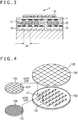
- the solid-state image pickup element 11, and the memory circuit 12 and logic circuit 13 arranged on the single layer are electrically connected via small-sized bumps 31.
- connection pitch d2 it is difficult to form the small-sized bumps 31, and, as depicted in FIG. 3 , there is a limitation on the size-reduction of a connection pitch d2, which make it impossible to make the connection pitch d2 smaller than a connection pitch d1 in FIG. 2 depicting the case that WoW is used.
- the solid-state image pickup apparatus 1 in FIG. 3 which is a stack formed by using bumps, cannot have a large number of connection terminals compared with the solid-state image pickup apparatus 1 in FIG. 2 , which is a stack formed by using WoW.
- the connection terminals are joined in an implementation process, and so deterioration of the yield related to the joining occurs, undesirably increasing the cost.
- the connection of the bumps in the implementation process requires work which is performed for each bump. Accordingly, each process takes a long time, and the process cost also increases.
- an image pickup element of the present disclosure is to reduce costs related to manufacturing, in terms of theoretical yield, implementation cost and process cost.
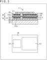
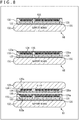
- FIG. 4 is a figure for explaining a structure that is to be applied at the time of the manufacturing of a solid-state image pickup apparatus of the present disclosure, and is a stack of plural wafers formed by using a combination of the CoW (Chip on Wafer) technology and the WoW technology.
- CoW Chip on Wafer
- CMOS Complementary Metal Oxide Semiconductor
- CCDs Charge Coupled Devices
- the other of the two wafers is a wafer 102 in which memory circuits 121 and logic circuits 122 are re-arranged.
- solid-state image pickup elements 120 are represented as being CMOS image sensors (CMOS Image Sensors) in figures, and are also referred to as CIS 120 simply.
- the wafer 101 has plural solid-state image pickup elements 120 formed therein by a semiconductor process.
- the wafer 102 has plural memory circuits 121 re-arranged therein.
- the plural memory circuits 121 are formed on a wafer 103 by a semiconductor process, and diced, and thereafter are each subjected to an electrical inspection, and confirmed to be good chips.
- the wafer 102 has plural logic circuits 122 re-arranged therein.
- the plural logic circuits 122 are formed on a wafer 104 by a semiconductor process, and diced, and thereafter are each subjected to an electrical inspection, and confirmed to be good chips.
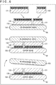
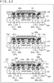
- the solid-state image pickup apparatus of the present disclosure has a configuration as depicted in FIG. 5 , for example.
- FIG. 5 includes a side cross-sectional view on the upper half, and a figure, on the lower half, depicting a horizontal arrangement relation among a solid-state image pickup element 120, a memory circuit 121, and a logic circuit 122 as seen from above.
- the solid-state image pickup apparatus 111 on the upper half of FIG. 5 color filters and on-chip lenses 131, and the solid-state image pickup element 120 are stacked from above in the figure. Thereunder, the memory circuit 121 and the logic circuit 122 are stacked being arranged on the left and right on a single layer. Thereunder, a support board 132 is formed. That is, as depicted on the upper half of FIG. 5 , the solid-state image pickup apparatus 111 in FIG. 5 includes a semiconductor element layer E1 including the solid-state image pickup element 120 formed on the wafer 101, and a semiconductor element layer E2 including the memory circuit 121 and the logic circuit 122 formed on the wafer 102.
- Wires 120a that are in wires 120a of the solid-state image pickup element 120, and are on the memory circuit 121 are electrically connected with wires 121a of the memory circuit 121 by wires 134 connected by CuCu-connection.
- wires 120a that are in the wires 120a of the solid-state image pickup element 120, and are on the logic circuit 122 are electrically connected with wires 122a of the logic circuit 122 by wires 134 connected by CuCu-connection.
- the oxide film 133 is an inorganic film, it is desirably a Si-based oxide film such as a SiO2 film, a SiO film, or a SRO film in terms of heat resistance and the warp amount after film formation.
- a Si-based oxide film such as a SiO2 film, a SiO film, or a SRO film in terms of heat resistance and the warp amount after film formation.
- an organic film in that case is preferably a polyimide-based (PI, PBO, etc.) film, a polyamide-based film or the like that can easily ensure high heat resistance.
- the semiconductor element layer E1 on which the solid-state image pickup element 120 is formed, and the semiconductor element layer E2 on which the memory circuit 121 and the logic circuit 122 are formed are joined at their boundary by an oxide film junction layer 135 formed by oxide-film joining. Further, the semiconductor element layer E2 including the memory circuit 121 and the logic circuit 122, and the support board 132 are joined by an oxide film junction layer 135 formed by oxide-film joining.
- the memory circuit 121 and the logic circuit 122 are arranged to be enclosed in an area where the solid-state image pickup element 120 is on the uppermost layer.
- the empty space not occupied by the memory circuit 121 and the logic circuit 122 decreases on the layer including the memory circuit 121 and the logic circuit 122, and so it becomes possible to enhance the theoretical yield.
- memory circuits 121 and logic circuits 122 are re-arranged being adjusted finely such that, when individual solid-state image pickup apparatuses 111 are formed by dicing, the memory circuits 121 and the logic circuits 122 are arranged in areas of solid-state image pickup elements 120 when seen from above.
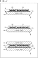
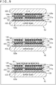
- FIG. 5 a method of manufacturing the solid-state image pickup apparatus 111 in FIG. 5 is explained with reference to FIG. 6 to FIG. 9 .
- side cross-sectional views 6A to 6L in FIG. 6 to FIG. 9 depict side cross-sectional views of the solid-state image pickup apparatus 111.
- the memory circuit 121 and the logic circuit 122 confirmed to be good elements after an electrical inspection is performed are re-arranged on a re-arrangement board 151 in the layout as depicted on the lower half of FIG. 5 .
- An adhesive 152 is applied onto the re-arrangement board 151, and the memory circuit 121 and the logic circuit 122 re-arranged on the re-arrangement board 151, and fixed by the adhesive 152.
- the memory circuit 121 and the logic circuit 122 are reversed such that their top surfaces depicted in the side cross-sectional view 6A become the lower surfaces, an oxide film is formed, and oxide-film joining is performed by forming the oxide film junction layer 135 on a flattened support board 161.
- the re-arrangement board 151 is debonded together with the adhesive 152, and peeled and eliminated.
- silicon layers at top surface sections, in the figure, of the memory circuit 121 and the logic circuit 122 are made thin such the height of the memory circuit 121 and the logic circuit 122 becomes a height A which does not influence the characteristics of the device.
- the oxide film 133 to function as an insulating film is formed, and a chip including the re-arranged memory circuit 121 and logic circuit 122 is embedded therein.
- the surface of the oxide film 133 is flattened at the height corresponding to the height of the memory circuit 121 and the logic circuit 122.
- a support board 171 is joined on the flattened oxide film 133 by the oxide film junction layer 135 formed by oxide-film joining.
- a seventh process as depicted in the side cross-sectional view 6G in FIG. 8 , the support board 171 is eliminated by being debonded or by being etched.
- the memory circuit 121 and the logic circuit 122 are re-arranged in the layout depicted on the lower half of FIG. 5 , and are embedded in the insulating film including the oxide film 133, and in this state the wafer 102 having the oxide film junction layer 135 formed on the flattened uppermost surface becomes completed state.
- wires 134 are formed for the wires 121a of the memory circuit 121, and the wires 122a of the logic circuit 122 for electrical connection with the solid-state image pickup element 120.
- the wires 134 from the wires 121a of the memory circuit 121, and the wires 122a of the logic circuit 122 on the wafer 102, and the wires 134 from the wires 120a of the solid-state image pickup element (CIS) 120 on the wafer 101 are aligned such that they are at appropriately facing positions.
- the wafers 101 and 102 are bonded by WoW such that the wires 134 from the wires 121a of the memory circuit 121, and the wires 122a of the logic circuit 122 on the wafer 102, and the wires 134 from the wires 120a of the solid-state image pickup element 120 on the wafer 101 are connected by CuCu-joining.
- each of the memory circuit 121 and the logic circuit 122 on the wafer 102 becomes electrically connected with each solid-state image pickup element 120 on the wafer 101.
- a silicon layer which is an upper layer, in the figure, of the solid-state image pickup element 120 is made thin.
- the color filters and on-chip lenses 131 are provided on the solid-state image pickup element 120, and diced. Thereby, the solid-state image pickup apparatus 111 is completed.
- the solid-state image pickup apparatus 111 including a first layer on which the solid-state image pickup element 120 is formed, and a second layer on which the memory circuit 121 and the logic circuit 122 are formed is manufactured.
- the inter-circuit connection between the solid-state image pickup element 120, and the memory circuit 121 and the logic circuit 122 can be formed by forming terminals at a wire density of very thin wires by the semiconductor lithography technology as in WoW. Accordingly, the number of connection terminals can be increased, the signal processing speed at each wire can be reduced, and so it becomes possible to attempt to reduce the power consumption.
- the memory circuit 121 and the logic circuit 122 to be connected can be arranged in an independent islandlike manner as depicted on the lower half of FIG. 5 by reducing their sizes as much as possible regardless of the chip size of the solid-state image pickup element 120. Accordingly, it becomes possible to enhance the theoretical yield of the memory circuit 121 and the logic circuit 122 to be connected.
- the solid-state image pickup element 120 requires a minimum necessary pixel size for reacting to optical light, and so the process cost can be reduced because the process of manufacturing the solid-state image pickup element 120 does not necessarily require fine wiring processes.
- circuits that are used may be other than the memory circuit 121 and the logic circuit 122, like circuits related to the control of the solid-state image pickup element 120, circuits related to the processing of pixel signals generated by image-capturing, and the like as long as those circuits are signal processing circuits considered to be required for the operation of the solid-state image pickup element 120.
- Examples of the signal processing circuits considered to be required for the operation of the solid-state image pickup element 120 may include, for example, a power supply circuit, an image signal compression circuit, a clock circuit, an optical communication conversion circuit and the like.
- the solid-state image pickup apparatus 111 explained above has a two-layer configuration including stacked layers, which are layer on which the solid-state image pickup element 120 is formed, and a layer on which the memory circuit 121 and the logic circuit 122 are re-arranged.
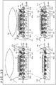
- FIG. 10 is a side cross-sectional view of the solid-state image pickup apparatus 111 more specifically representing internal terminals and wires of each of the solid-state image pickup element (CIS) 120, the memory circuit 121 and the logic circuit 122 included in the solid-state image pickup apparatus 111 depicted in FIG. 5 .
- the oxide film junction layer 135 is omitted from illustrations, but is present.
- pads 120b and 121b electrically connected with the wires 120a and 121a, respectively are mutually CuCu-joined.
- pads 120b and 122b electrically connected with wires 120a and 122a, respectively are mutually CuCu-connected.
- each pad 120b of the solid-state image pickup element 120 is connected to various types of circuit, a wire 120a or another pad 120b via a wire 120c.
- each pad 121b of the memory circuit 121 is connected to a wire 121a via a wire 121c.
- each pad 122b of the logic circuit 122 is connected to a wire 122a via a wire 122c.
- each wire 134 in FIG. 5 has a configuration which is an aggregation of wires 120c, pads 120b and 121b, and wires 121c.
- pads 122b-1 and 122b-2 of the logic circuit 122 are CuCu-joined with pads 120b-1 and 120b-2 of the solid-state image pickup element 120
- pads 121b-2 and 121b-1 of the memory circuit 121 are CuCu-joined with pads 120b-3 and 120b-4 of the solid-state image pickup element 120.
- the pad 120b-1 of the solid-state image pickup element 120 is connected with a wire 120c-1.
- the pads 120b-2 and 120b-3 are interconnected via a wire 120c-2.
- a pad 120c-4 is connected with a wire 120c-3.
- the solid-state image pickup element 120 and the memory circuit 121 are electrically connected via the wire 120c-2.
- the memory circuit 121 and the logic circuit 122 are connected via the wire 120c-2 in the solid-state image pickup element 120 with the largest chip area size.
- the wire 120c-2 functions as a communication wire between the memory circuit 121 and the logic circuit 122.
- the configuration of wires is explained by referring to a configuration which has the wire 120c-2 to be the communication wire as the center of the configuration, and includes selected pads and wires which are the pad 120b-1 to 120b-4 and the wires 120c-1 to 120c-3 of the solid-state image pickup element 120, the wires 121a-1 and 121a-2, the pads 121b-1 and 121b-2, and the wires 121c-1 and 121c-2 of the memory circuit 121, and the wires 122a-1 and 122a-2, the pads 122b-1 and 122b-2, and the wires 122c-1 and 122c-2 of the logic circuit 122.
- the memory circuit 121 and the logic circuit 122 are electrically connected via the wire (pad) 121a-2, the wire 121c-2, the pads 121b-2 and 120b-3, the wire 120c-2, the pads 120b-2 and 122b-2, the wire 122c-2, and the wire (pad) 122a-2.
- a communication wire connecting the memory circuit 121 and the logic circuit 122 is formed in the semiconductor element layer E2 on which the memory circuit 121 and the logic circuit 122 are formed, and the pads 121b and 122b are mutually electrically connected.
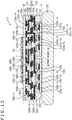
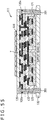
- the solid-state image pickup apparatus 111 in FIG. 12 is different from the solid-state image pickup apparatus 111 in FIG. 10 in terms of the configuration of the semiconductor element layer E2.
- pads 120b-11 to 120b-14 and wires 120c-11 and 120c-14 of the solid-state image pickup element 120 in the configuration in FIG. 12 correspond to the pads 120b-1 to 120b-4 and the wires 120c-1 and 120c-3 of the solid-state image pickup element 120 in FIG. 10 , respectively.
- wires 121a-11 and 121a-12, pads 121b-11 and 121b-12, and wires 121c-11 and 121c-12 of the memory circuit 121 in FIG. 12 correspond to the wires 121a-1 and 121a-2, the pads 121b-1 and 121b-2, and the wires 121c-1 and 121c-2 of the memory circuit 121 in FIG. 10 , respectively.
- wires 122a-11 and 122a-12, pads 122b-11 and 122b-12, and wires 122c-11 and 122c-12 of the logic circuit 122 in FIG. 12 correspond to the wires 122a-1 and 122a-2, the pads 122b-1 and 122b-2, and the wires 122c-1 and 122c-2 of the logic circuit 122 in FIG. 10 , respectively.
- a wiring layer is formed between the memory circuit 121 and the logic circuit 122, and the pads 121b and 122b, and wires 121c'-1 and 122c'-1 which are extensions of the wires 121c and 122c are formed.
- a communication wire T that connects a wire 121c-12 of the memory circuit 121, and a wire 122c-12 of the logic circuit 122 is formed.
- the total area size of the memory circuit 121 and the logic circuit 122 is smaller than that of the solid-state image pickup element 120, and so it becomes possible to expand the wire pitch of 121c'-1 and 122c'-1 to the extent as allowed by the area size of the solid-state image pickup element 120 as depicted in FIG. 12 , for example, by using unoccupied areas.
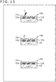
- Step S11 Logic FEOL
- a wiring pattern is formed on a board of each logic circuit 122 by FEOL (Front-End-Of-Line: board process) on the wafer 104 in FIG. 4 , for example.
- Step S12 In a process in Step S12 (Logic_BEOL), wires are formed with a metal such as AL or Cu along the wiring pattern on the board of the logic circuit 122 by BEOL (Back-End-Of-Line: wiring process).
- a metal such as AL or Cu along the wiring pattern on the board of the logic circuit 122 by BEOL (Back-End-Of-Line: wiring process).
- Step S13 Logic_Inspection (KGD)
- a measurement terminal C is used to perform an inspection of the wires (pads) 122c of the logic circuit 122, and on the basis of results of the inspection, a logic circuit 122 to be a good element is selected.
- Step S14 the wires (pads) 122c of the logic circuit 122 are embedded in a Si oxide film 122L by plasma CVD (Chemical Vapor Deposition).
- Step S15 flatten embedment
- embedment steps LD (see the side cross-sectional view 15B) formed with the Si oxide film 122L of the logic circuit 122 are polished and flattened by CMP (Chemical Mechanical Polishing).
- Step S16 logic Dicing
- logic circuits 122 on the wafer 104 are separated into pieces by dicing, and good elements are extracted.
- Steps S11 to S16 the logic circuit 122 is manufactured.
- Step S21 Memory FEOL
- a wiring pattern is formed on a board of each memory circuit 121 by FEOL (Front-End-Of-Line: board process) on the wafer 103 in FIG. 4 , for example.
- Step S22 Memory BEOL
- wires are formed with a metal such as AL or Cu along the wiring pattern on the board of the memory circuit 121 by BEOL (Back-End-Of-Line: wiring process).
- Step S23 Memory Inspection (KGD: Known Good Die)
- the measurement terminal C is used to perform an inspection of the wires (pads) 121c of the memory circuit 121, and on the basis of results of the inspection, a memory circuit 121 to be a good element is selected.
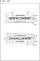
- Step S24 (embed pad), as depicted in a side cross-sectional view 16B in FIG. 16 , the wires (pads) 121c of the memory circuit 121 are embedded in a Si oxide film 121M by plasma CVD (Chemical Vapor Deposition).
- plasma CVD Chemical Vapor Deposition
- Step S25 flatten embedment
- embedment steps MD see the side cross-sectional view 16B
- CMP Chemical Mechanical Polishing
- Step S26 Memory Dicing
- logic circuits 122 on the wafer 103 are separated into pieces by dicing, and good elements are extracted.
- the memory circuit 121 is manufactured.
- Step S31 Memory die CoW
- a junction Si oxide film is formed on the re-arrangement board 151 by CVD, and the memory circuit 121 is temporarily connected such that a surface thereof provided with wires (pads) 121c abuts against the junction Si oxide film (Face down).
- Examples of the connection method for the temporary connection include oxide-film joining such as plasma joining.
- a method other than oxide-film joining such as plasma joining may be used, and, for example, a commercially available temporary joint tape or the like may be used. Note that it becomes possible to enhance the connection quality by forming an alignment mark for each CoW in advance on the side of the re-arrangement board 151.
- Step S32 (Logic die CoW)
- the logic circuit 122 is temporarily connected such that a surface thereof provided with wires (pads) 122c abuts against the re-arrangement board 151 (Face down).
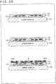
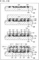
- Step S33 (embed die), as depicted in a side cross-sectional view 17C in FIG. 17 , a gap between the memory circuit 121 and the logic circuit 122 is filled (partially) with the oxide film 133 by plasma CVD, and the diced memory circuit 121 and logic circuit 122 are fixed to the re-arrangement board 151.
- Step S34 make die thin
- Si boards of the diced memory circuit 121 and logic circuit 122 are made thin. More specifically, grinding is performed at high speed by a grinder, and CMP is performed for a surface quality improvement.
- Step S35 the oxide film 133 is formed until steps are filled again by plasma CVD or the like for the purpose of filling the gap between the memory circuit 121 and logic circuit 122 having been made thin.
- Step S36 (embedment surface CMP), as depicted in a side cross-sectional view 18C in FIG. 18 , a step KD formed on the surfaces of the memory circuit 121 and the logic circuit 122 is flattened by CMP. At this time, the memory circuit 121 and the logic circuit 122 are finished such that their Si film thicknesses are within the range approximately of 1 to 10 um.
- the memory circuit 121 and the logic circuit 122 are re-arranged on the re-arrangement board 151 and are embedded in the oxide film 133.
- Step S41 permanently join WoW
- the support board 132 on which a Si oxide film is formed is permanently joined by plasma joining on the memory circuit 121 and the logic circuit 122 re-arranged on the re-arrangement board 151.
- Step S42 debond re-arrangement board
- the re-arrangement board 151 is debonded and peeled.
- Step S43 form communication wire
- the oxide film 133 is further accumulated additionally.
- the communication wire T to connect the memory circuit 121 and the logic circuit 122 is formed.
- Step S44 form Cu-Cu connection wire (etc.)
- pads 121b and 122b for electrical connection with the solid-state image pickup element 120 are formed.
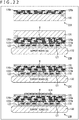
- the communication wire T may include plural wires depending on the pitches of the pads 121b and 122b as represented by communication wires T1 to T5 as depicted in FIG. 21 .
- the communication wires may be formed in an area outside the arrangement area of the memory circuit 121 and the logic circuit 122.
- the pads 121b and 122b may be formed on a grid in the area of the solid-state image pickup element 120 to be stacked thereafter.
- the communication wires may be connected to another circuit or the like other than the memory circuit 121 and the logic circuit 122 as represented by a communication wire T6 such that the memory circuit 121 or the logic circuit 122 is individually connected with another circuit.
- FIG. 21 includes a top view of the support board 132 on the upper half, and a side view of the support board 132 on the lower half.
- an area surrounded by a dotted line in the top view in FIG. 21 is an area on which the solid-state image pickup element 120 is to be stacked.
- the memory circuit 121 and the logic circuit 122 are connected by the communication wire T, and further the pads 121b and 122b for connection with the solid-state image pickup element 120 are formed.
- Step S51 a wiring pattern is formed on a board of each solid-state image pickup element 120 by FEOL (Front-End-Of-Line: board process) on the wafer 101 in FIG. 4 , for example.
- FEOL Front-End-Of-Line: board process
- Step S52 Logic BEOL
- wires are formed with a metal such as AL or Cu along the wiring pattern on the board of the solid-state image pickup element 120 by BEOL (Back-End-Of-Line: wiring process).
- Step S53 flatten embedment
- the pads 120b of the solid-state image pickup element 120 are embedded in a Si oxide film by plasma CVD (Chemical Vapor Deposition), and embedment steps including the Si oxide film are polished and flattened by CMP (Chemical Mechanical Polishing).
- Step S54 form Cu-Cu connection wire (etc.)
- the pads 120b for electrical connection with the solid-state image pickup element 120 are formed, and the wafer 101 of the solid-state image pickup element 120 is completed.
- the solid-state image pickup element 120 is manufactured by the processes in Steps S51 to S54.
- Step S61 permanent (Cu-Cu joining WoW)
- the pads 120b of the solid-state image pickup element 120, and the pads 121b of the memory circuit and the pads 122b of the logic circuit 122 are CuCu-joined (direct joining).
- Step S62 backside CIS process
- the solid-state image pickup element 120 is made thin, and a protective film is formed.
- the color filters and on-chip lenses 131 are formed.
- the solid-state image pickup apparatus 111 in FIG. 12 formed with the communication wire of the memory circuit 121 and the logic circuit 122 not going through the solid-state image pickup element 120 is manufactured.
- the communication wire T of the memory circuit 121 and the logic circuit 122 is formed in the semiconductor element layer E2, and on a side of the boundary with the solid-state image pickup element 120, it may be formed in another area as long as it is possible to join the memory circuit 121 and the logic circuit 122.
- the communication wire may be formed in the semiconductor element layer E2, and on a side of the boundary with the support board 132.
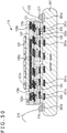
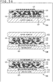
- FIG. 23 depicts the solid-state image pickup apparatus 111 in which a communication wire T' is formed in the semiconductor element layer E2, and on a side of the boundary with the support board 132.
- the solid-state image pickup apparatus 111 in FIG. 23 is similar to the solid-state image pickup apparatus 111 in FIG. 12 in other respects than that the communication wire T' is formed in the memory circuit 121 and the logic circuit 122, and on a side of the boundary with the support board 132, and so an explanation regarding a method of manufacturing the solid-state image pickup apparatus 111 in FIG. 23 is omitted.
- connections between the solid-state image pickup element 120, and the memory circuit 121 and the logic circuit 122 are formed between wires CuCu-joined with the pads 120b and the pads 121b and 122b connected at a junction surface F2.
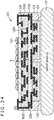
- the solid-state image pickup element 120, and the memory circuit 121 are connected by a through-electrode TCV1
- the solid-state image pickup element 120 and the logic circuit 122 are connected by a through-electrode TCV2.
- the through-electrodes TCV1 and TCV2 include Cu, and insulating films are formed on surfaces thereof.
- the memory circuit 121 is provided with a pad 121b to be connected with the through-electrode TCV1
- the logic circuit 122 is provided with a pad 122b to be connected with the through-electrode TCV2.
- the pad 121b of the memory circuit 121, and the pad 122b of the logic circuit 122 are formed when the communication wire T is formed.
- wires can be placed in spaces in which the pad 120b in the solid-state image pickup element 120, the pad 121b of the memory circuit 121 and the pad 122b of the logic circuit 122 are provided, it becomes possible to reduce the resistance of wires, and to reduce the power consumption.
- Steps S71, S72, S81 to S83, S91, and S93 in FIG. 25 are similar to the processes in Steps S41, S42, S51 to S53, S61, and S62 explained with reference to FIG. 14 , and so explanations thereof are omitted.
- the communication wire T is formed in a process in Step S73 (form communication wire (etc.)).
- the pad 121b of the memory circuit 121, and the pad 122b of the logic circuit 122 for the connection with the through-electrodes TCV1 and TCV2 are formed at positions corresponding to the through-electrodes TCV1 and TCV2.
- Step S92 connect vertical die (TCV)
- TCV1 and TCV2 are formed at the positions of the through-electrodes TCV1 and TCV2 in FIG. 24 through the Si board of the solid-state image pickup element 120, and thereafter the through-holes are filled with Cu, and formed as electrodes.
- the solid-state image pickup apparatus 111 in FIG. 24 is manufactured.
- wires can be placed in spaces in which the pad 120b in the solid-state image pickup element 120, the pad 121b of the memory circuit 121, and the pad 122b of the logic circuit 122 are provided, it becomes possible to reduce the resistance of wires, and to reduce the power consumption.
- junction surface F2 is formed in a state in which the wiring layer side of the memory circuit 121 and the logic circuit 122, and the wiring layer side of the solid-state image pickup element 120 are facing each other, through-electrodes may be formed on a surface (a surface on the side of the Si board) opposite to the wiring layers of the memory circuit 121 and the logic circuit 122, and joined with the solid-state image pickup element 120.
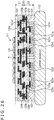
- FIG. 26 depicts the solid-state image pickup apparatus 111 in which through-electrodes TSV (Through Silicon Via) are formed on a surface opposite to the wiring layers of the memory circuit 121 and the logic circuit 122, and joined with the solid-state image pickup element 120.
- TSV Through Silicon Via
- the solid-state image pickup apparatus 111 in FIG. 26 is different from the solid-state image pickup apparatus 111 in FIG. 12 in that the memory circuit 121 and the logic circuit 122 are vertically reversed in the figure, and have through-electrodes 121d and 122d formed on the backsides thereof (the Si-board sides thereof to be the top surfaces in FIG. 26 ), and wires 121c' and 122c' are connected to the pads 121b and 122b via through-electrodes (TSV).
- TSV through-electrodes
- Steps S111 to S114 which are the processes of manufacturing the solid-state image pickup element 120 are similar to the processes in Steps S51 to S54 in FIG. 14 , and so explanations thereof are omitted.
- the re-arrangement board 151 is not used as described below, there are no processes related to the re-arrangement board 151.
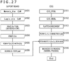
- Step S101 Memory_die CoW
- a junction Si oxide film is formed on the support board 132 by CVD, and the memory circuit 121 is connected such that a surface thereof provided with wires (pads) 121c abuts against the junction Si oxide film (Face down).
- the connection method include oxide-film joining such as plasma joining.
- connection for the connection, a method other than oxide-film joining such as plasma joining may be used, and, for example, a commercially available temporary joint tape or the like may be used. Note that it becomes possible to enhance the connection quality by forming an alignment mark for each CoW in advance on the side of the re-arrangement board 151.
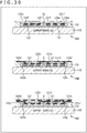
- Step S102 (Logic die CoW), as depicted in a side cross-sectional view 28B in FIG. 28 , the logic circuit 122 is connected such that a surface thereof provided with wires 122c abuts against the support board 132 (Face down).
- Step S103 make die thin
- a gap between the memory circuit 121 and the logic circuit 122 is filled (partially) with the oxide film 133 by plasma CVD, and the diced memory circuit 121 and logic circuit 122 are fixed to the support board 132.
- Si boards of the diced memory circuit 121 and logic circuit 122 are made thin. More specifically, grinding is performed at high speed by a grinder, and CMP is performed for a surface quality improvement.
- Step S104 the oxide film 133 is formed until steps are filled again by plasma CVD or the like for the purpose of filling the gap between the memory circuit 121 and logic circuit 122 having been made thin.
- a step KD formed on the surfaces of the memory circuit 121 and the logic circuit 122 is flattened by CMP.
- the memory circuit 121 and the logic circuit 122 are finished such that their Si film thicknesses are within the range approximately of 1 to 10 um.
- the memory circuit 121 and the logic circuit 122 are re-arranged on the support board 132 and are embedded in the oxide film 133.
- Step S105 (rewire & form pad) plasma SiO2 is formed such that the thickness becomes approximately 100 to 1500 nm for the purpose of insulating the Si films of the memory circuit 121 and the logic circuit 122 after CMP.
- groove sections 121e, 122e, and Te corresponding to wires to connect the memory circuit 121 and the logic circuit 122 are formed by resist patterning and oxide film dry etching.
- the groove sections 121e, 122e, and Te are formed down to depths that do not reach Si of the memory circuit 121 and the logic circuit 122.
- through-holes 121f and 122f are formed as openings to reach depths immediately before reaching copper wires of the lowermost layer in the multi-layer wiring layer, or as openings to reach depths immediately before reaching Al pads at the uppermost layer, such that the through-holes 121f and 122f penetrate Si of the memory circuit 121 and the logic circuit 122 from the areas of the groove sections 121e and 122e formed in the manner described above.
- the diameters of the through-holes 121f and 122f are approximately 1 to 5 um, for example.
- insulating films including SiO2 are formed on the side walls of Si exposed as a result of the processing described above, and thereafter an etch-back process is performed to thereby eliminate SiO2 formed as protective films of bottom sections of the through-holes 121f and 122f, and make the wiring layers of the memory circuit 121 and the logic circuit 122 exposed.
- a metal such as Cu is embedded in the through-holes 121f and 122f, the surfaces are polished by CMP (Chemical Mechanical Polishing), and only the conductive materials of the groove sections 121e, 122e, and Te and the through-holes 121f and 122f are left.
- the communication wire T that connects the memory circuit 121 and the logic circuit 122, and lead wires 121c' and 122c' from the through-electrodes 121d and 122d of the memory circuit 121 and the logic circuit 122 are formed in areas in the insulating spacer layer.
- the pads 121b and 122b for CuCu-joining (hybrid-joining) with the solid-state image pickup element 120 are formed.
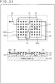
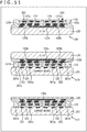
- the communication wire T may include plural wires depending on the pitches of the pads 121b and 122b as represented by the communication wires T1 to T5 in FIG. 31 .
- the communication wires may be formed in an area that is in the arrangement area of the solid-state image pickup element 120, and outside the arrangement area of the memory circuit 121 and the logic circuit 122.
- the pads 121b and 122b may be formed on a grid in the area of the solid-state image pickup element 120 to be stacked thereafter.
- the communication wires may be connected to another circuit or the like other than the memory circuit 121 and the logic circuit 122 as represented by the communication wire T6 such that the memory circuit 121 or the logic circuit 122 is individually connected with another circuit.
- FIG. 31 includes a top view of the support board 132 on the upper half, and a side view of the support board 132 on the lower half.
- an area surrounded by a dotted line in the top view in FIG. 31 is an area on which the solid-state image pickup element 120 is to be stacked.
- the memory circuit 121 and the logic circuit 122 are connected by the communication wire T, and further the pads 121b and 122b for connection with the solid-state image pickup element 120 are formed.
- Step S111 to Step S114 form Cu-Cu connection wire (etc.)
- the pads 120b for electrical connection with the pads 121b and 122b of the memory circuit 121 and the logic circuit 122 are formed, and the wafer 101 of the solid-state image pickup element 120 is completed.
- Step S115 permanent (Cu-Cu joining WoW)
- the pads 120b of the solid-state image pickup element 120, and the pads 121b of the memory circuit and the pads 122b of the logic circuit 122 are CuCu-joined (direct joining).
- Step S116 backside CIS process
- the solid-state image pickup element 120 is made thin, and a protective film is formed.
- the color filters and on-chip lenses 130 are formed.
- the solid-state image pickup apparatus 111 in FIG. 12 formed with the communication wire of the memory circuit 121 and the logic circuit 122 not going through the solid-state image pickup element 120 is manufactured.
- a wiring layer is formed in each of the memory circuit 121, the logic circuit 122, and the solid-state image pickup element 120, and the junction surface F2 is formed in a state in which the memory circuit 121, the logic circuit 122, and the solid-state image pickup element 120 are facing one another
- a wiring layer may be formed also on the support board 132, and a communication wire between the memory circuit 121 and the logic circuit 122 may be formed on the wiring layer on the support board 132.
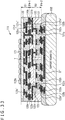
- FIG. 33 depicts a configuration example of the solid-state image pickup apparatus 111 in which a wiring layer is formed also on the support board 132, and a communication wire between the memory circuit 121 and the logic circuit 122 is formed via the wiring layer on the support board 132.
- the solid-state image pickup apparatus 111 in FIG. 33 has a configuration that is different from the configuration of the solid-state image pickup apparatus 111 in FIG. 26 in that the solid-state image pickup element 120, and the memory circuit 121 and the logic circuit 122 are electrically connected at a junction surface F4-1, and the memory circuit 121 and the logic circuit 122, and the support board are electrically connected at a junction surface F4-2.
- the memory circuit 121 and the logic circuit 122 have pads 121b' and 122b' formed therein on surfaces thereof that face the support board 132, and at positions corresponding to pads 132b forming the wiring layer of the support board 132.
- the support board 132 has the pads 132b formed at positions facing the memory circuit 121 and the logic circuit 122, and further wires 132a, and a communication wire T'' between the memory circuit 121 and the logic circuit 122 are formed at a lower section in FIG. 33 .
- the wires 132a can be used for electrical connection and can also be used for positioning by being used as alignment marks.
- the pads 132b of the support board 132, the pads 121b' of the memory circuit 121, and the pads 122b' of the logic circuit 122 are CuCu-connected.
- communication wires between the memory circuit 121 and the logic circuit 122 include the two communication wires T and T'', but only any one of them may be provided.
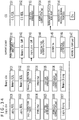
- Steps S11 to S16 the processes of manufacturing the memory circuit 121 and the logic circuit 122 are similar to Steps S11 to S16, and Steps S21 to S26 in the flowchart in FIG. 14 except for the processes in Steps S126 and S136, and so explanations thereof are omitted.
- Steps S142 to S147 which are the processes related to the support board 132 are similar to the processes in Steps S101 to S106 in FIG. 27 , and so explanations thereof are omitted.
- Steps S151 to S154 which are the processes of manufacturing the solid-state image pickup element 120 are similar to the processes in Steps S51 to S54 in FIG. 14 , and so explanations thereof are omitted.
- Step S126 form Cu-Cu connection pad
- the pads 122b' for CuCu-joining with the pads 132b of the support board 132 are formed as depicted in a side cross-sectional view 35B in FIG. 35 .
- the pads 122b' are formed by a technique that is similar to the technique used in the case the through-electrodes 122d, the wire 122c', and the pads 122b' in the solid-state image pickup apparatus 111 in FIG. 26 are formed in the process in Step S106 explained with reference to the flowchart in FIG. 27 .
- the logic circuit 122 on the wafer 104 is diced, and a good element is extracted.
- Step S136 the pads 121b' are formed in the memory circuit 121 also by a similar technique, the memory circuit 121 is diced, and a good element is extracted.
- Step S141 form communication wire (etc.)
- the wires 132a, the communication wire T'', and the pads 132b are formed on the support board 132.
- a thermal oxide film, LP-SiN or the like is formed on the support board (bare Si) 132 not having a device structure, and is insulated from Si.
- plasma SiO2 is formed to have a thickness of approximately 100 to 1500 nm, a wiring pattern for inter-chip connection with the line pitch width of 0.5 to 5 um is formed by resist-patterning depending on the layout of the pads 121b' and 122b' of the memory circuit 121 and the logic circuit 122, and a groove section with the depth of 100 to 1000 nm is formed by dry etching.
- the pads 132b for CuCu-connection are formed by a technique similar to the technique used in the case where the through-electrodes 122d, the wire 122c', and the pads 122b are formed.
- Steps S142 and S143 Memory_die CoW, Logic_die CoW
- the pads 121b' and 122b' of the memory circuit 121 and the logic circuit 122 are CuCu-joined (direct joining), and electrically connected such that the pads 121b' and 122b' of the memory circuit 121 and the logic circuit 122 are at positions corresponding to the positions of the pads 132b.
- Step S144 make die thin
- a gap between the memory circuit 121 and the logic circuit 122 is filled (partially) with the oxide film 133 by plasma CVD, and the diced memory circuit 121 and logic circuit 122 are fixed to the support board 132.
- Si boards of the diced memory circuit 121 and logic circuit 122 are made thin. More specifically, grinding is performed at high speed by a grinder, and CMP is performed for a surface quality improvement.
- Step S145 (embed dei), as depicted in a side cross-sectional view 37B in FIG. 37 , the oxide film 133 is formed until steps are filled again by plasma CVD or the like for the purpose of filling the gap between the memory circuit 121 and logic circuit 122 having been made thin.
- a step formed on the surfaces of the memory circuit 121 and the logic circuit 122 is flattened by CMP. At this time, the memory circuit 121 and the logic circuit 122 are finished such that their Si film thicknesses are within the range approximately of 1 to 10 um.
- Step S146 plasma SiO2 is formed such that the thickness becomes approximately 100 to 1500 nm for the purpose of insulating the Si films of the memory circuit 121 and the logic circuit 122 after CMP.
- the groove sections 121e, 122e, and Te corresponding to wires to connect the memory circuit 121 and the logic circuit 122 are formed by resist patterning and oxide film dry etching.
- the groove sections 121e, 122e, and Te are formed down to depths that do not reach Si of the memory circuit 121 and the logic circuit 122.
- the through-holes 121f and 122f are formed as openings to reach depths immediately before reaching copper wires of the lowermost layer in the multi-layer wiring layer, or as openings to reach depths immediately before reaching Al pads at the uppermost layer, such that the through-holes 121f and 122f penetrate Si of the memory circuit 121 and the logic circuit 122 from the areas of the groove sections 121e and 122e formed in the manner described above.
- the diameters of the through-holes 121f and 122f are approximately 1 to 5 um, for example.
- Step S147 (rewire & form pad), as depicted in a side cross-sectional view 37D in FIG. 37 , insulating films including SiO2 are formed on the side walls of Si exposed as a result of the processing described above, and thereafter an etch-back process is performed to thereby eliminate SiO2 formed as protective films of bottom sections of the through-holes 121f and 122f, and make the wiring layers of the memory circuit 121 and the logic circuit 122 exposed.
- a metal such as Cu is embedded in the through-holes 121f and 122f, the surfaces are polished by CMP (Chemical Mechanical Polishing), and only the conductive materials of the groove sections 121e, 122e, and Te and the through-holes 121f and 122f are left.
- the communication wire T that connects the memory circuit 121 and the logic circuit 122, and lead wires 121c' and 122c' from the through-electrodes 121d and 122d of the memory circuit 121 and the logic circuit 122 are formed in areas in the insulating spacer layer.
- the pads 121b and 122b for hybrid (Cu-Cu) connection with the solid-state image pickup element 120 are formed.
- the memory circuit 121 and the logic circuit 122 are connected by the communication wires T and T'', and further the pads 121b and 122b for connection with the solid-state image pickup element 120 are formed.
- Step S151 to Step S154 form Cu-Cu connection wire (etc.)
- the pads 120b are formed, and the wafer 101 of the solid-state image pickup element 120 is completed.
- Step S155 permanent (Cu-Cu joining WoW)
- the pads 120b of the solid-state image pickup element 120, and the pads 121b of the memory circuit and the pads 122b of the logic circuit 122 are CuCu-joined.
- Step S156 backside CIS process
- the solid-state image pickup element 120 is made thin, and a protective film is formed.
- the color filters and on-chip lenses 130 are formed.
- the solid-state image pickup apparatus 111 in FIG. 33 formed with the communication wires T and T'' of the memory circuit 121 and the logic circuit 122 not going through the solid-state image pickup element 120 is manufactured.
- the memory circuit 121 and the logic circuit 122 are re-arranged on the support board 132 including the communication wires, and the solid-state image pickup element 120 is stacked in the solid-state image pickup apparatus 111 in the explanation above; however, in another possible configuration, the logic circuit 122 may be stacked on a memory device board having the function of the memory circuit 121 instead of the support board 132, and the solid-state image pickup element 120 may be stacked on the logic circuit 122.
- FIG. 39 depicts a configuration example of the solid-state image pickup apparatus 111 in which the logic circuit 122 is stacked on a memory device board having the function of the memory circuit 121 instead of the support board 132, and the solid-state image pickup element 120 is stacked on the logic circuit 122.
- the logic circuit 122 is stacked on the memory device board 201 such that the logic circuit 122 is embedded in the oxide film 133, and further the solid-state image pickup element 120 is stacked on the logic circuit 122.
- the solid-state image pickup element 120, and the logic circuit 122 and the memory device board 201 are CuCu-joined and electrically connected at a junction surface F5-1 through the pads 120b, and the pads 201b' and 122b.
- the pads 201b', wires 201c, and through-electrodes 201d are formed in a state in which the pads 201b', the wires 201c, and the through-electrodes 201d are connected with each other, and the pads 201b of the memory device board 201, and the through-electrodes 201d are connected at a junction surface F5-2.
- the memory device 201 and the solid-state image pickup element 120 are electrically connected via the pads 201b', the wires 201c and the through-electrodes 201d, and the pads 201b.
- the logic circuit 122 and the memory device board 201 are CuCu-joined and electrically connected at the junction surface F5-2 through the pads 201b and 122b. Stated differently, the CuCu-joined pads 201b and 122b substantially function as communication wires.
- the memory device board 201 having the function of the memory circuit 121 is provided, and is stacked such that the logic circuit 122 is sandwiched between the memory device board 201 and the solid-state image pickup element 120.
- a logic device board having the function of the logic circuit 122 may be provided, and stacked such that the memory circuit 121 is sandwiched between the logic device board and the solid-state image pickup element 120, in another possible configuration.
- Steps S191 to S194 which are the processes of manufacturing the solid-state image pickup element 120 are similar to the processes in Steps S51 to S54 in the flowchart in FIG. 14 , and so explanations thereof are omitted.
- a wiring pattern for realizing the function as the memory circuit 121 is formed on the memory device board 201, and wires are formed with a metal such as AL or Cu.
- Step S172 Memory BEOL
- good dies and bad dies may be clearly identified in advance.
- Step S173 In a process in Step S173 (rewire & form Cu-Cu connection pad), wires 201a and the pads 201b are formed. Here, alignment marks for connection are formed also.
- Step S174 (Logic die CoW), as depicted in a side cross-sectional view 41A in FIG. 41 , the pads 201b of the memory device board 201, and the pads 122b' of the logic circuit 122 are CuCu-joined. Note that, while an example in which only the logic circuit 122 is connected is explained with reference to FIG. 41 , plural circuit chips may be connected depending on functions.
- Step S175 make die thin
- the space around the logic circuit 122 on the memory device board 201 is filled with the oxide film 133 to thereby fix the logic circuit 122 onto the memory device board 201, and thereafter the logic circuit 122 is made thin.
- Step S176 (embed die), as depicted in a side cross-sectional view 41B in FIG. 41 , by repeating the process in Step S175, the logic circuit 122 is embedded in the oxide film 133.
- Steps S177 and S178 form TSV, form memory connection via
- the through-electrodes 122d that penetrate Si of the logic circuit 122, and the through-electrodes 201d for connection with the memory device board 201 are formed.
- an insulating film 221 including plasma SiO2 is formed such that the thickness becomes 100 to 1500 nm, for the purpose of insulating Si after CMP.
- an area where the pads 201b', the wires 201c and the through-electrodes 201d to connect the memory device board 201 and the solid-state image pickup element 120 are formed, and groove sections 222 that are corresponding to intra-stack connecting wires to be used when the solid-state image pickup element 120 and the logic circuit 122 are connected are formed by resist patterning and oxide film dry etching. At this time, the groove sections 222 are formed with depths that do not reach Si of the logic circuit 122 and the memory device 201.
- vias 223 for connection with the memory device board 201, and vias 224 for connection with the logic circuit 122 are formed by patterning, and dry etching of the oxide film 133 is performed first.
- the vias 224 reach Si while the vias 223 of the memory device board 201 are being formed, but because the selection ratio of SiO2 and Si is high, Si is not processed, and the vias 223 and 224 with different depths are formed.
- the etching condition is changed, and the vias 223 and 224 are processed. That is, after the processing resists are eliminated, the insulating film 221 including plasma SiO2 for insulating Si is formed, and thereafter an etch-back process performed. Thereby, vias 223' and 254' are formed simultaneously as depicted in a side cross-sectional view 42C in FIG. 42 .
- Step S179 (rewire & form pad), as depicted in a side cross-sectional view 43A in FIG. 43 , after a barrier metal is formed, a metal such as Cu is embedded in the vias 223' and 224', and the surfaces are polished by CMP (Chemical Mechanical Polishing).
- CMP Chemical Mechanical Polishing
- pads 201b and 122b for CuCu-connection with the solid-state image pickup element 120 are formed.
- Step S195 permanently (Cu-Cu) join WoW
- the pads 120b of the solid-state image pickup element 120, and the pads 201b and 122b' of the memory device board 201 and the logic circuit 122 are CuCu-joined.
- Step S196 backside CIS process
- the solid-state image pickup element 120 is made thin, and a protective film is formed.
- the color filters and on-chip lenses 131 are formed.
- the solid-state image pickup apparatus 111 manufactured by the processes above it becomes possible to reduce the number of processes before the solid-state image pickup element 120 with a large area size is joined, and it is possible to enhance the yield according to the reduction of processes.
- the memory circuit 121 and the logic circuit 122 are stacked on the re-arrangement board 151 or the support board 132 and are embedded in the oxide film 133, and the solid-state image pickup element 120 is stacked on the memory circuit 121 and the logic circuit 122, to thereby manufacture the solid-state image pickup apparatus 111.
- the memory circuit 121 and the logic circuit 122 may be stacked on the solid-state image pickup element 120 and be embedded in the oxide film 133, and the support board 132 may be stacked on the memory circuit 121 and the logic circuit 122.
- the configuration of the completed solid-state image pickup apparatus 111 is basically similar to that in FIG. 10 .
- the memory circuit 121 and the logic circuit 122 are stacked on the solid-state image pickup element 120 and are embedded in the oxide film 133, and the support board 132 is stacked on the memory circuit 121 and the logic circuit 122.
- the wires 120a and the pads 120b are formed in the solid-state image pickup element 120.
- the memory circuit 121 and the logic circuit 122 are stacked on the solid-state image pickup element 120, and the pads 120b, and the pads 121b and 122b are CuCu-joined.
- oxide-film connection is performed after a hydrophilic treatment, connection at the normal temperature is possible at the time of the CuCu-connection, and it becomes possible to highly precisely ensure the alignment between the solid-state image pickup element 120, and the memory circuit 121 and the logic circuit 122.
- the alignment precision is at a level that can satisfy 1 um ⁇ 3 ⁇ .
- the memory circuit 121 is tilted, and is caused to partially abut against the solid-state image pickup element 120. In this state, the whole is joined.
- the side cross-sectional view 44B in FIG. 44 depicts a state where only the memory circuit 121 is tilted, and is caused to partially abut against the solid-state image pickup element 120
- the logic circuit 122 is also implemented by a similar technique.
- Si of the memory circuit 121 and the logic circuit 122 is made thin.
- the memory circuit 121 and the logic circuit 122 are made as thin as possible before the embedment process using the oxide film 133, or the like.
- the thicknesses of the memory circuit 121 and the logic circuit 122 are preferably made equal to or thinner than approximately 20 um, for example.
- the memory circuit 121 and the logic circuit 122 are embedded in the oxide film 133.
- the oxide film 133 is an inorganic film, it is desirably a Si-based oxide film such as a SiO2 film, a SiO film, or a SRO film in terms of heat resistance and the warp amount after film formation.
- the oxide film 133 is preferably a polyimide-based (PI, PBO, etc.) oxide film, a polyamide-based oxide film or the like that can easily ensure high heat resistance.
- groove sections 121e', 122e', and Te' corresponding to wires to connect the memory circuit 121 and the logic circuit 122 are formed by resist patterning and oxide film dry etching.
- the groove sections 121e', 122e', and Te' are formed down to depths that do not reach Si of the memory circuit 121 and the logic circuit 122.
- through-holes 121f' and 122f' are formed as openings to reach depths immediately before reaching copper wires of the lowermost layer in the multi-layer wiring layer, or as openings to reach depths immediately before reaching Al pads at the uppermost layer, such that the through-holes 121f' and 122f' penetrate Si of the memory circuit 121 and the logic circuit 122 from the areas of the groove sections 121e' and 122e' formed in the manner described above.
- the diameters of the through-holes 121f' and 122f' are approximately 1 to 5 um, for example.
- insulating films including SiO2 are formed on the side walls of Si exposed as a result of the processing described above, and thereafter an etch-back process is performed to thereby eliminate SiO2 formed as protective films of bottom sections of the through-holes 121f' and 122f', and make the wiring layers of the memory circuit 121 and the logic circuit 122 exposed.
- a metal such as Cu is embedded in the through-holes 121f' and 122f', the surfaces are polished by CMP (Chemical Mechanical Polishing), and only the conductive materials of the groove sections 121e', 122e', and Te' and the through-holes 121f' and 122f' are left.
- CMP Chemical Mechanical Polishing
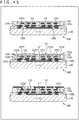
- a communication wire T''' that connects the memory circuit 121 and the logic circuit 122, and through-electrodes 121d' and 122d' of the memory circuit 121 and the logic circuit 122 are formed in areas in the insulating spacer layer.
- a seventh process as depicted in a side cross-sectional view 46A in FIG. 46 , the solid-state image pickup element 120, the memory circuit 121, and the logic circuit 122 in the state depicted in the side cross-sectional view 45C in FIG. 45 are reversed vertically, and are connected onto the support board 132.
- the Si board of the solid-state image pickup element 120 is made thin, and thereafter the color filters and on-chip lenses 131 are formed.
- an organic photoelectric conversion film 241 may be formed between the on-chip lenses 131 and the solid-state image pickup element 120.
- the heat proof temperature of the organic photoelectric conversion film 241 is low, and cannot endure a solder connection temperature which requires heating at 200°C or higher.
- the seventh embodiment of the present disclosure it is possible to form the less heat-resistant organic photoelectric conversion film 241 after the stacking of chips, and a technology of fine CuCu joining can be applied. Accordingly, it becomes possible to realize the solid-state image pickup apparatus 111 including the solid-state image pickup element 120 having low dark current characteristics, while maintaining a high external quantum efficiency.
- the memory circuit 121 and the logic circuit 122 are arrayed and stacked on the solid-state image pickup element 120, and are embedded in the oxide film 133, and the support board 132 is stacked on the memory circuit 121 and the logic circuit 122, to thereby manufacture the solid-state image pickup apparatus 111.
- the solid-state image pickup apparatus 111 may be manufactured by stacking and arranging the memory circuit 121 and the logic circuit 122 on the solid-state image pickup element 120, embedding the memory circuit 121 and the logic circuit 122 in the oxide film 133, and stacking the support board 132 on the stacked memory circuit 121 and logic circuit 122.
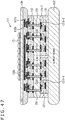
- FIG. 47 depicts a configuration example of the solid-state image pickup apparatus 111 manufactured by stacking and arranging the memory circuit 121 and the logic circuit 122 on the solid-state image pickup element 120, embedding the memory circuit 121 and the logic circuit 122 in the oxide film 133, and stacking the support board 132 on the memory circuit 121 and logic circuit 122.
- the logic circuit 122 is stacked on the support board 132, further two memory circuits 121-1 and 121-2 are arrayed in the horizontal direction and stacked on the logic circuit 122, and then the solid-state image pickup element 120 is stacked on the memory circuits 121-1 and 121-2.
- through-electrodes (TSV) 231 and 232 are formed in the memory circuits 121-1 and 121-2, the solid-state image pickup element 120 and the logic circuit 122 are electrically connected via the through-electrodes 231, and the memory circuit 121 and the logic circuit 122 are electrically connected via the through-electrodes 232. That is, the through-electrodes 232 function as communication wires.
- the order in which the memory circuit 121 and the logic circuit 122 are stacked may be reversed, and, for example, the memory circuit 121 and the logic circuit 122 in FIG. 47 may be vertically reversed, in one possible configuration.
- the solid-state image pickup apparatus 111 can be manufactured by stacking the good memory circuit 121 and logic circuit 122 in such a configuration also, it is possible to enhance the theoretical yield, and it becomes possible to reduce the cost.
- plural layers of memory circuits 121 and logic circuits 122 may be stacked further by a similar technique, and so it becomes possible to realize a capacity increase of a memory.
- the solid-state image pickup element 120, the memory device board 201 and the logic circuit 122 have been manufactured similarly to the memory circuit 121 and the logic circuit 122, and the logic circuit 122 has been diced, and selected as a good element as a result of an inspection.
- the wires 120a and the pads 120b are formed in the solid-state image pickup element 120.
- the logic circuit 122 is stacked on the solid-state image pickup element 120, and the pads 120b and the pads 122b are CuCu-joined.
- Si of the logic circuit 122 is made thin, and the through-electrodes 231 and 232 are formed.
- the through-electrodes 231 are connected with the pads 120b of the solid-state image pickup element 120, and the through-electrodes 232 are connected with the pads 122b of the logic circuit.
- the memory circuits 121-1 and 121-2 are arranged being arrayed on the logic circuit 122, and the through-electrodes 231 and 232, and the pads 121b-1 and 121b-2 of the memory circuits 121-1 and 121-2 are CuCu-connected.
- the memory circuits 121-1 and 121-2 are formed being embedded in the oxide film 133, and further surfaces of the memory circuits 121-1 and 121-2 are flattened by CMP.
- a sixth process as depicted in a side cross-sectional view 49B in FIG. 49 , the state in the side cross-sectional view 49A is reversed vertically, and the memory circuits 121-1 and 121-2 are connected and fixed onto the support board 132.
- the Si board of the solid-state image pickup element 120 is made thin, and thereafter the color filters and on-chip lenses 131 are formed.
- the memory circuits 121 are stacked at a necessary number of stages by repeating the fourth and fifth processes explained with reference to the side cross-sectional view 48D in FIG. 48 , and the side cross-sectional view 49A in FIG. 49 .
- the solid-state image pickup apparatus 111 manufactured by the processes above also can be manufactured by stacking the good memory circuit 121 and logic circuit 122, it is possible to enhance the theoretical yield, and it becomes possible to reduce the cost.
- a wiring layer may be formed on the side of the support board, and terminals of wire bonding may be formed.
- FIG. 50 depicts a configuration example of the solid-state image pickup apparatus 111 in which a wiring layer is formed on the side of the support board, and terminals of wire bonding are formed.
- the solid-state image pickup apparatus 111 in FIG. 50 has a configuration in which wires 261a are formed in a support board 261 and are electrically connected with terminals 261b at left and right end sections.
- the wires 261a are connected with the wires 121a and 122a via through-electrodes 251 and 252 that penetrate the Si boards of the memory circuit 121 and the logic circuit 122.
- the pads 121b and 122b of the memory circuit 121 and the logic circuit 122 are CuCu-joined with the wires 120a of the solid-state image pickup element 120, the wires 261a are electrically connected also with the solid-state image pickup element 120 via the memory circuit 121 and the logic circuit 122.
- the terminals 261b are provided with bonding sections 271 to which wires 272 are connected, and the solid-state image pickup apparatus 111 has a configuration that can transmit and receive signals to and from an external apparatus via the wires 272 via the bonding sections 271.
- FIG. 50 a method of manufacturing the solid-state image pickup apparatus 111 in FIG. 50 is explained with reference to FIG. 51 and FIG. 52 . Note that it is assumed that the solid-state image pickup element 120, the memory circuit 121, and the logic circuit 122 have been manufactured, and the memory circuit 121 and the logic circuit 122 have been diced, and selected as good elements as a result of an inspection.
- the through-electrodes 251 and 252 are formed to the wires 121a and 122a in the Si boards of the memory circuit 121 and the logic circuit 122.
- a second process as depicted in a side cross-sectional view 51B in FIG. 51 , the configuration in the side cross-sectional view 51A in FIG. 51 is vertically reversed, and is joined to the support board 261 in which the wires 261a and the terminals 261b are formed. At this time, the through-electrodes 251 and 252 are joined with the wires 261a of the support board 261.
- the Si board of the solid-state image pickup element 120 is made thin.
- the color filters and on-chip lenses 131 are formed on the solid-state image pickup element 120.
- the oxide film 133 and the solid-state image pickup element 120 that are in upper sections of the terminals 261b surrounded by dotted lines in the figure are partially cut out, and the terminals 261b are made exposed.
- the wires 272 are connected with the terminals 261b via the bonding sections 271, and the solid-state image pickup apparatus 111 is completed.
- the space required for handling in order to cope with the bending of the wires 272 increases, and so the distance to the lens 281 needs to be a distance A.
- the space required for handling of the wires 272 can be made small as depicted in an upper right section in FIG. 53 , and so the distance between the solid-state image pickup element 120 and the lens 281 can be made a distance B shorter than the distance A.
- the through-electrodes 251 and 252 are formed from the memory circuit 121 and the logic circuit 122, respectively, and signals from the solid-state image pickup element 120 are output to the outside via the wires 272 connected to the bonding sections 271 via the memory circuit 121 and the logic circuit 122, and the wires 261a and the terminals 261b of the support board 261.
- through-electrodes 291 that penetrate the oxide film 133 without penetrating the memory circuit 121 and the logic circuit 122, and connect the pads 120b of the solid-state image pickup element 120, and the wires 261a of the support board 261 may be formed.
- the solid-state image pickup element 120, and the wires 261a of the support board 261 are connected directly via the through-electrodes 291. It should be noted however that, in this case, the memory circuit 121 and the logic circuit 122 become not electrically connected with the support board 261, but output to the outside is possible via wires in the solid-state image pickup element 120, and the through-electrodes 291.
- the through-electrodes 291 that connect the pads 120b of the solid-state image pickup element 120, and the wires 261a of the support board 261, the through-electrodes 251 that connect the wires 121a of the memory circuit 121, and the wires 261a, and the through-electrodes 251 that connect the wires 122a of the logic circuit 122, and the wires 261a may be provided.
- the solid-state image pickup element 120, the memory circuit 121, and the logic circuit 122 are individually independently electrically connected with the support board 261, and so it becomes unnecessary to provide communication wires and the like.
- output to the outside may not be performed via the support board 261 via the through-electrodes 251, 252, and 271, and terminals may be provided in the electrically connected state in a wiring layer in the memory circuit 121 and the logic circuit 122 on which the pads 121b and 122b are provided.
- terminals 261b' in the electrically connected state are provided in the wiring layer in the memory circuit 121 and the logic circuit 122 on which the pads 121b and 122b are provided.
- FIG. 55 depicts a configuration example of the solid-state image pickup apparatus 111 that can output signals directly from through-electrodes 301 connected to the solid-state image pickup element 120 from the backside of the support board 132, without going through the memory circuit 121 and the logic circuit 122.
- FIG. 55 a method of manufacturing the solid-state image pickup apparatus 111 in FIG. 55 is explained with reference to FIG. 56 and FIG. 57 .
- a side cross-sectional view 56A in FIG. 56 depicts a state where the solid-state image pickup apparatus 111 in FIG. 12 has been manufactured.
- An explanation is given regarding the solid-state image pickup apparatus 111 in FIG. 55 assuming that it is generated by processing the solid-state image pickup apparatus 111 in FIG. 12 .
- a first process as depicted in a side cross-sectional view 56B in FIG. 56 , the configuration in the side cross-sectional view 56A in FIG. 56 is vertically reversed, and is placed on a backing board 311 via an interference section 312 which includes a resin that can protect the color filters and on-chip lenses 131 on the solid-state image pickup element 120, and is resistant to heat that is equal to or higher than 250°C, or the like.
- the support board 132 is made thin.
- the through-electrodes 301 are formed such that they penetrate the oxide film 133 from above the support board 132, and reach the wires 120a of the solid-state image pickup element 120.
- a fourth process as depicted in a side cross-sectional view 57B in FIG. 57 , the surface of the solid-state image pickup element 120 including the color filters and on-chip lenses 131 is peeled off from the interference section 312, and the configuration is reversed vertically as depicted in a side cross-sectional view 57C to thereby complete the solid-state image pickup apparatus 111 in FIG. 55 .
- through-electrodes are each formed separately in layers, and stacked.
- through-electrodes 371 with predetermined depths are formed in advance on the support board 132 at positions corresponding to the through-electrodes 301 in FIG. 55 . Then, as depicted in a side cross-sectional view 58A in FIG. 58 , in a state in which the support board 132 is vertically reversed, the support board 132 is fixed onto the memory circuit 121 and the logic circuit 122 placed on the re-arrangement board 151.
- the memory circuit 121 and the logic circuit 122 are embedded in the oxide film 133, and flattened.
- through-electrodes 381 are formed in the oxide film 133 at positions corresponding to the through-electrodes 301 in FIG. 55 . That is, the through-electrodes 381 become electrically connected with the through-electrodes 371.
- a fifth process after through-electrodes 391 are formed at positions corresponding to the through-electrodes 301 in FIG. 55 of the solid-state image pickup element 120, as depicted in a side cross-sectional view 59B in FIG. 59 , the state is vertically reversed, and the through-electrodes 391 are joined onto the memory circuit 121 and the logic circuit 122. That is, the through-electrodes 391 become electrically connected with the through-electrodes 381. That is, by the processes up to this point, the through-electrodes 371, 381, and 391 are configured as integrated through-electrodes.
- the solid-state image pickup element 120 is made thin, and thereafter the color filters and on-chip lenses 131 are formed on the image pickup surface.
- a seventh process as depicted in a side cross-sectional view 60A in FIG. 60 , the configuration in the side cross-sectional view 59C in FIG. 59 in the vertically reversed state is placed on the backing board 311 via the interference section 312 which includes a resin that can protect the color filters and on-chip lenses 131 on the solid-state image pickup element 120, and is resistant to heat that is equal to or higher than 250°C, or the like.
- the support board 132 is made thin, and top sections of the through-electrodes 371 are exposed.
- the interference section 312 is peeled off from the surface of the solid-state image pickup element 120 including the color filters and on-chip 131, and the configuration is reversed vertically to thereby complete the solid-state image pickup apparatus 111 in FIG. 55 .
- through-electrodes 401 and 402 may be formed from the backside of the support board 132 such that they are connected to the wires 121a and 122a of the memory circuit 121 and the logic circuit 122, respectively, included in the solid-state image pickup apparatus 111.
- the method of manufacturing the solid-state image pickup apparatus 111 in FIG. 61 is similar to that in a case where the through-electrodes 301 or the through-electrodes 371, 381, and 391 are formed in the method of manufacturing the solid-state image pickup apparatus 111 in FIG. 55 , and so an explanation thereof is omitted.
- the image pickup element mentioned above can be applied to various types of electronic equipment like image pickup apparatuses such as a digital still camera or a digital video camera, mobile phones having the image pickup function, or other equipment having the image pickup function.
- FIG. 62 is a block diagram depicting a configuration example of an image pickup apparatus as electronic equipment to which the present technology is applied.
- An image pickup apparatus 501 depicted in FIG. 62 includes an optical system 502, a shutter apparatus 503, a solid-state image pickup element 504, a drive circuit 505, a signal processing circuit 506, a monitor 507, and a memory 508, and can capture still image images and moving images.
- the optical system 502 includes one lens or plural lenses, guides light from a subject (incident light) to the solid-state image pickup element 504, and causes an image to be formed on the light-receiving surface of the solid-state image pickup element 504.
- the shutter apparatus 503 is arranged between the optical system 502 and the solid-state image pickup element 504, and, under the control of the drive circuit 505, controls the light emission period and light blocking period of light into the solid-state image pickup element 504.
- the solid-state image pickup element 504 includes a package including the solid-state image pickup element mentioned above.
- the solid-state image pickup element 504 accumulates a signal charge for a predetermined period according to light to form an image on the light-receiving surface after going through the optical system 502 and the shutter apparatus 503.
- the signal charge accumulated in the solid-state image pickup element 504 is transferred according to a drive signal (timing signal) supplied from the drive circuit 505.
- the drive circuit 505 outputs drive signals to control the transfer operation of the solid-state image pickup element 504, and the shutter operation of the shutter apparatus 503, and drives the solid-state image pickup element 504 and the shutter apparatus 503.
- the signal processing circuit 506 performs various types of signal processing on a signal charge output from the solid-state image pickup element 504.
- An image (image data) obtained by the signal processing performed by the signal processing circuit 506 is supplied to and displayed on the monitor 507, or is supplied to and stored (recorded) on the memory 508, for example.
- FIG. 63 is a figure depicting use examples in which the solid-state image pickup apparatus 111 mentioned above is used.
- the solid-state image pickup apparatus mentioned above can be used in various cases in which light such as visible light, infrared light, ultraviolet light, or X-ray is sensed, like the following ones, for example.
- the technology according to the present disclosure (the present technology) can be applied to various products.
- the technology according to the present disclosure may be applied to endoscopic surgery systems.
- FIG. 64 is a view depicting an example of a schematic configuration of an endoscopic surgery system to which the technology according to an embodiment of the present disclosure (present technology) can be applied.
- FIG. 64 a state is illustrated in which a surgeon (medical doctor) 11131 is using an endoscopic surgery system 11000 to perform surgery for a patient 11132 on a patient bed 11133.
- the endoscopic surgery system 11000 includes an endoscope 11100, other surgical tools 11110 such as a pneumoperitoneum tube 11111 and an energy device 11112, a supporting arm apparatus 11120 which supports the endoscope 11100 thereon, and a cart 11200 on which various apparatus for endoscopic surgery are mounted.
- the endoscope 11100 includes a lens barrel 11101 having a region of a predetermined length from a distal end thereof to be inserted into a body cavity of the patient 11132, and a camera head 11102 connected to a proximal end of the lens barrel 11101.
- the endoscope 11100 is depicted which includes as a rigid endoscope having the lens barrel 11101 of the hard type.
- the endoscope 11100 may otherwise be included as a flexible endoscope having the lens barrel 11101 of the flexible type.
- the lens barrel 11101 has, at a distal end thereof, an opening in which an objective lens is fitted.
- a light source apparatus 11203 is connected to the endoscope 11100 such that light generated by the light source apparatus 11203 is introduced to a distal end of the lens barrel 11101 by a light guide extending in the inside of the lens barrel 11101 and is irradiated toward an observation target in a body cavity of the patient 11132 through the objective lens.
- the endoscope 11100 may be a forward-viewing endoscope or may be an oblique-viewing endoscope or a side-viewing endoscope.
- An optical system and an image pickup element are provided in the inside of the camera head 11102 such that reflected light (observation light) from the observation target is condensed on the image pickup element by the optical system.
- the observation light is photo-electrically converted by the image pickup element to generate an electric signal corresponding to the observation light, namely, an image signal corresponding to an observation image.
- the image signal is transmitted as RAW data to a CCU 11201.
- the CCU 11201 includes a central processing unit (CPU), a graphics processing unit (GPU) or the like and integrally controls operation of the endoscope 11100 and a display apparatus 11202. Further, the CCU 11201 receives an image signal from the camera head 11102 and performs, for the image signal, various image processes for displaying an image based on the image signal such as, for example, a development process (demosaic process).
- a development process demosaic process
- the display apparatus 11202 displays thereon an image based on an image signal, for which the image processes have been performed by the CCU 11201, under the control of the CCU 11201.
- the light source apparatus 11203 includes a light source such as, for example, a light emitting diode (LED) and supplies irradiation light upon imaging of a surgical region to the endoscope 11100.
- a light source such as, for example, a light emitting diode (LED) and supplies irradiation light upon imaging of a surgical region to the endoscope 11100.
- LED light emitting diode
- An inputting apparatus 11204 is an input interface for the endoscopic surgery system 11000.
- a user can perform inputting of various kinds of information or instruction inputting to the endoscopic surgery system 11000 through the inputting apparatus 11204.
- the user would input an instruction or a like to change an image pickup condition (type of irradiation light, magnification, focal distance or the like) by the endoscope 11100.
- a treatment tool controlling apparatus 11205 controls driving of the energy device 11112 for cautery or incision of a tissue, sealing of a blood vessel or the like.
- a pneumoperitoneum apparatus 11206 feeds gas into a body cavity of the patient 11132 through the pneumoperitoneum tube 11111 to inflate the body cavity in order to secure the field of view of the endoscope 11100 and secure the working space for the surgeon.
- a recorder 11207 is an apparatus capable of recording various kinds of information relating to surgery.
- a printer 11208 is an apparatus capable of printing various kinds of information relating to surgery in various forms such as a text, an image or a graph.
- the light source apparatus 11203 which supplies irradiation light when a surgical region is to be imaged to the endoscope 11100 may include a white light source which includes, for example, an LED, a laser light source or a combination of them.
- a white light source includes a combination of red, green, and blue (RGB) laser light sources, since the output intensity and the output timing can be controlled with a high degree of accuracy for each color (each wavelength), adjustment of the white balance of a picked up image can be performed by the light source apparatus 11203.
- RGB red, green, and blue
- the light source apparatus 11203 may be controlled such that the intensity of light to be outputted is changed for each predetermined time.
- driving of the image pickup element of the camera head 11102 in synchronism with the timing of the change of the intensity of light to acquire images time-divisionally and synthesizing the images an image of a high dynamic range free from underexposed blocked up shadows and overexposed highlights can be created.
- the light source apparatus 11203 may be configured to supply light of a predetermined wavelength band ready for special light observation.
- special light observation for example, by utilizing the wavelength dependency of absorption of light in a body tissue to irradiate light of a narrow band in comparison with irradiation light upon ordinary observation (namely, white light), narrow band observation (narrow band imaging) of imaging a predetermined tissue such as a blood vessel of a superficial portion of the mucous membrane or the like in a high contrast is performed.
- fluorescent observation for obtaining an image from fluorescent light generated by irradiation of excitation light may be performed.
- fluorescent observation it is possible to perform observation of fluorescent light from a body tissue by irradiating excitation light on the body tissue (autofluorescence observation) or to obtain a fluorescent light image by locally injecting a reagent such as indocyanine green (ICG) into a body tissue and irradiating excitation light corresponding to a fluorescent light wavelength of the reagent upon the body tissue.
- a reagent such as indocyanine green (ICG)
- ICG indocyanine green
- the light source apparatus 11203 can be configured to supply such narrowband light and/or excitation light suitable for special light observation as described above.
- FIG. 65 is a block diagram depicting an example of a functional configuration of the camera head 11102 and the CCU 11201 depicted in FIG. 64 .
- the camera head 11102 includes a lens unit 11401, an image pickup unit 11402, a driving unit 11403, a communication unit 11404 and a camera head controlling unit 11405.
- the CCU 11201 includes a communication unit 11411, an image processing unit 11412 and a control unit 11413.
- the camera head 11102 and the CCU 11201 are connected for communication to each other by a transmission cable 11400.
- the lens unit 11401 is an optical system, provided at a connecting location to the lens barrel 11101. Observation light taken in from a distal end of the lens barrel 11101 is guided to the camera head 11102 and introduced into the lens unit 11401.
- the lens unit 11401 includes a combination of a plurality of lenses including a zoom lens and a focusing lens.
- the number of image pickup elements which is included by the image pickup unit 11402 may be one (single-plate type) or a plural number (multi-plate type). Where the image pickup unit 11402 is configured as that of the multi-plate type, for example, image signals corresponding to respective R, G and B are generated by the image pickup elements, and the image signals may be synthesized to obtain a color image.
- the image pickup unit 11402 may also be configured so as to have a pair of image pickup elements for acquiring respective image signals for the right eye and the left eye ready for three dimensional (3D) display. If 3D display is performed, then the depth of a living body tissue in a surgical region can be comprehended more accurately by the surgeon 11131. It is to be noted that, where the image pickup unit 11402 is configured as that of stereoscopic type, a plurality of systems of lens units 11401 are provided corresponding to the individual image pickup elements.
- the image pickup unit 11402 may not necessarily be provided on the camera head 11102.
- the image pickup unit 11402 may be provided immediately behind the objective lens in the inside of the lens barrel 11101.
- the driving unit 11403 includes an actuator and moves the zoom lens and the focusing lens of the lens unit 11401 by a predetermined distance along an optical axis under the control of the camera head controlling unit 11405. Consequently, the magnification and the focal point of a picked up image by the image pickup unit 11402 can be adjusted suitably.
- the communication unit 11404 includes a communication apparatus for transmitting and receiving various kinds of information to and from the CCU 11201.
- the communication unit 11404 transmits an image signal acquired from the image pickup unit 11402 as RAW data to the CCU 11201 through the transmission cable 11400.
- the communication unit 11404 receives a control signal for controlling driving of the camera head 11102 from the CCU 11201 and supplies the control signal to the camera head controlling unit 11405.
- the control signal includes information relating to image pickup conditions such as, for example, information that a frame rate of a picked up image is designated, information that an exposure value upon image picking up is designated and/or information that a magnification and a focal point of a picked up image are designated.
- the image pickup conditions such as the frame rate, exposure value, magnification or focal point may be designated by the user or may be set automatically by the control unit 11413 of the CCU 11201 on the basis of an acquired image signal.
- an auto exposure (AE) function, an auto focus (AF) function and an auto white balance (AWB) function are incorporated in the endoscope 11100.
- the camera head controlling unit 11405 controls driving of the camera head 11102 on the basis of a control signal from the CCU 11201 received through the communication unit 11404.
- the communication unit 11411 includes a communication apparatus for transmitting and receiving various kinds of information to and from the camera head 11102.
- the communication unit 11411 receives an image signal transmitted thereto from the camera head 11102 through the transmission cable 11400.
- the communication unit 11411 transmits a control signal for controlling driving of the camera head 11102 to the camera head 11102.
- the image signal and the control signal can be transmitted by electrical communication, optical communication or the like.
- the image processing unit 11412 performs various image processes for an image signal in the form of RAW data transmitted thereto from the camera head 11102.
- the control unit 11413 performs various kinds of control relating to image picking up of a surgical region or the like by the endoscope 11100 and display of a picked up image obtained by image picking up of the surgical region or the like. For example, the control unit 11413 creates a control signal for controlling driving of the camera head 11102.
- control unit 11413 controls, on the basis of an image signal for which image processes have been performed by the image processing unit 11412, the display apparatus 11202 to display a picked up image in which the surgical region or the like is imaged.
- control unit 11413 may recognize various objects in the picked up image using various image recognition technologies.
- the control unit 11413 can recognize a surgical tool such as forceps, a particular living body region, bleeding, mist when the energy device 11112 is used and so forth by detecting the shape, color and so forth of edges of objects included in a picked up image.
- the control unit 11413 may cause, when it controls the display apparatus 11202 to display a picked up image, various kinds of surgery supporting information to be displayed in an overlapping manner with an image of the surgical region using a result of the recognition. Where surgery supporting information is displayed in an overlapping manner and presented to the surgeon 11131, the burden on the surgeon 11131 can be reduced and the surgeon 11131 can proceed with the surgery with certainty.
- the transmission cable 11400 which connects the camera head 11102 and the CCU 11201 to each other is an electric signal cable ready for communication of an electric signal, an optical fiber ready for optical communication or a composite cable ready for both of electrical and optical communications.
- communication is performed by wired communication using the transmission cable 11400
- the communication between the camera head 11102 and the CCU 11201 may be performed by wireless communication.
- the technology according to the present disclosure can be applied to the endoscope 11100, (the image pickup unit 11402 of) the camera head 11102 and the like in the configurations explained above.
- the solid-state image pickup apparatus 111 of the present disclosure can be applied to the image pickup unit 10402.
- the technology according to the present disclosure can be applied to various products.
- the technology according to the present disclosure may be realized as an apparatus to be mounted on any type of mobile body such as an automobile, an electric automobile, a hybrid electric automobile, a motorcycle, a bicycle, a personal mobility, an airplane, a drone, a ship, or a robot.
- FIG. 66 is a block diagram depicting an example of schematic configuration of a vehicle control system as an example of a mobile body control system to which the technology according to an embodiment of the present disclosure can be applied.
- the vehicle control system 12000 includes a plurality of electronic control units connected to each other via a communication network 12001.
- the vehicle control system 12000 includes a driving system control unit 12010, a body system control unit 12020, an outside-vehicle information detecting unit 12030, an in-vehicle information detecting unit 12040, and an integrated control unit 12050.
- a microcomputer 12051, a sound/image output section 12052, and a vehicle-mounted network interface (I/F) 12053 are illustrated as a functional configuration of the integrated control unit 12050.
- the driving system control unit 12010 controls the operation of devices related to the driving system of the vehicle in accordance with various kinds of programs.
- the driving system control unit 12010 functions as a control device for a driving force generating device for generating the driving force of the vehicle, such as an internal combustion engine, a driving motor, or the like, a driving force transmitting mechanism for transmitting the driving force to wheels, a steering mechanism for adjusting the steering angle of the vehicle, a braking device for generating the braking force of the vehicle, and the like.
- the body system control unit 12020 controls the operation of various kinds of devices provided to a vehicle body in accordance with various kinds of programs.
- the body system control unit 12020 functions as a control device for a keyless entry system, a smart key system, a power window device, or various kinds of lamps such as a headlamp, a backup lamp, a brake lamp, a turn signal, a fog lamp, or the like.
- radio waves transmitted from a mobile device as an alternative to a key or signals of various kinds of switches can be input to the body system control unit 12020.
- the body system control unit 12020 receives these input radio waves or signals, and controls a door lock device, the power window device, the lamps, or the like of the vehicle.
- the outside-vehicle information detecting unit 12030 detects information about the outside of the vehicle including the vehicle control system 12000.
- the outside-vehicle information detecting unit 12030 is connected with an imaging section 12031.
- the outside-vehicle information detecting unit 12030 makes the imaging section 12031 image an image of the outside of the vehicle, and receives the imaged image.
- the outside-vehicle information detecting unit 12030 may perform processing of detecting an object such as a human, a vehicle, an obstacle, a sign, a character on a road surface, or the like, or processing of detecting a distance thereto.
- the imaging section 12031 is an optical sensor that receives light, and which outputs an electric signal corresponding to a received light amount of the light.
- the imaging section 12031 can output the electric signal as an image, or can output the electric signal as information about a measured distance.
- the light received by the imaging section 12031 may be visible light, or may be invisible light such as infrared rays or the like.
- the in-vehicle information detecting unit 12040 detects information about the inside of the vehicle.
- the in-vehicle information detecting unit 12040 is, for example, connected with a driver state detecting section 12041 that detects the state of a driver.
- the driver state detecting section 12041 for example, includes a camera that images the driver.
- the in-vehicle information detecting unit 12040 may calculate a degree of fatigue of the driver or a degree of concentration of the driver, or may determine whether the driver is dozing.
- the microcomputer 12051 can calculate a control target value for the driving force generating device, the steering mechanism, or the braking device on the basis of the information about the inside or outside of the vehicle which information is obtained by the outside-vehicle information detecting unit 12030 or the in-vehicle information detecting unit 12040, and output a control command to the driving system control unit 12010.
- the microcomputer 12051 can perform cooperative control intended to implement functions of an advanced driver assistance system (ADAS) which functions include collision avoidance or shock mitigation for the vehicle, following driving based on a following distance, vehicle speed maintaining driving, a warning of collision of the vehicle, a warning of deviation of the vehicle from a lane, or the like.
- ADAS advanced driver assistance system
- the microcomputer 12051 can perform cooperative control intended for automatic driving, which makes the vehicle to travel autonomously without depending on the operation of the driver, or the like, by controlling the driving force generating device, the steering mechanism, the braking device, or the like on the basis of the information about the outside or inside of the vehicle which information is obtained by the outside-vehicle information detecting unit 12030 or the in-vehicle information detecting unit 12040.
- the microcomputer 12051 can output a control command to the body system control unit 12020 on the basis of the information about the outside of the vehicle which information is obtained by the outside-vehicle information detecting unit 12030.
- the microcomputer 12051 can perform cooperative control intended to prevent a glare by controlling the headlamp so as to change from a high beam to a low beam, for example, in accordance with the position of a preceding vehicle or an oncoming vehicle detected by the outside-vehicle information detecting unit 12030.
- the sound/image output section 12052 transmits an output signal of at least one of a sound and an image to an output device capable of visually or auditorily notifying information to an occupant of the vehicle or the outside of the vehicle.
- an audio speaker 12061, a display section 12062, and an instrument panel 12063 are illustrated as the output device.
- the display section 12062 may, for example, include at least one of an on-board display and a head-up display.
- FIG. 67 is a diagram depicting an example of the installation position of the imaging section 12031.
- the imaging section 12031 includes imaging sections 12101, 12102, 12103, 12104, and 12105.
- the imaging sections 12101, 12102, 12103, 12104, and 12105 are, for example, disposed at positions on a front nose, sideview mirrors, a rear bumper, and a back door of the vehicle 12100 as well as a position on an upper portion of a windshield within the interior of the vehicle.
- the imaging section 12101 provided to the front nose and the imaging section 12105 provided to the upper portion of the windshield within the interior of the vehicle obtain mainly an image of the front of the vehicle 12100.
- the imaging sections 12102 and 12103 provided to the sideview mirrors obtain mainly an image of the sides of the vehicle 12100.
- the imaging section 12104 provided to the rear bumper or the back door obtains mainly an image of the rear of the vehicle 12100.
- the imaging section 12105 provided to the upper portion of the windshield within the interior of the vehicle is used mainly to detect a preceding vehicle, a pedestrian, an obstacle, a signal, a traffic sign, a lane, or the like.
- FIG. 67 depicts an example of photographing ranges of the imaging sections 12101 to 12104.
- An imaging range 12111 represents the imaging range of the imaging section 12101 provided to the front nose.
- Imaging ranges 12112 and 12113 respectively represent the imaging ranges of the imaging sections 12102 and 12103 provided to the sideview mirrors.
- An imaging range 12114 represents the imaging range of the imaging section 12104 provided to the rear bumper or the back door.
- a bird's-eye image of the vehicle 12100 as viewed from above is obtained by superimposing image data imaged by the imaging sections 12101 to 12104, for example.
- At least one of the imaging sections 12101 to 12104 may have a function of obtaining distance information.
- at least one of the imaging sections 12101 to 12104 may be a stereo camera constituted of a plurality of imaging elements, or may be an imaging element having pixels for phase difference detection.
- the microcomputer 12051 can determine a distance to each three-dimensional object within the imaging ranges 12111 to 12114 and a temporal change in the distance (relative speed with respect to the vehicle 12100) on the basis of the distance information obtained from the imaging sections 12101 to 12104, and thereby extract, as a preceding vehicle, a nearest three-dimensional object in particular that is present on a traveling path of the vehicle 12100 and which travels in substantially the same direction as the vehicle 12100 at a predetermined speed (for example, equal to or more than 0 km/hour). Further, the microcomputer 12051 can set a following distance to be maintained in front of a preceding vehicle in advance, and perform automatic brake control (including following stop control), automatic acceleration control (including following start control), or the like. It is thus possible to perform cooperative control intended for automatic driving that makes the vehicle travel autonomously without depending on the operation of the driver or the like.
- automatic brake control including following stop control
- automatic acceleration control including following start control
- the microcomputer 12051 can classify three-dimensional object data on three-dimensional objects into three-dimensional object data of a two-wheeled vehicle, a standard-sized vehicle, a large-sized vehicle, a pedestrian, a utility pole, and other three-dimensional objects on the basis of the distance information obtained from the imaging sections 12101 to 12104, extract the classified three-dimensional object data, and use the extracted three-dimensional object data for automatic avoidance of an obstacle.
- the microcomputer 12051 identifies obstacles around the vehicle 12100 as obstacles that the driver of the vehicle 12100 can recognize visually and obstacles that are difficult for the driver of the vehicle 12100 to recognize visually. Then, the microcomputer 12051 determines a collision risk indicating a risk of collision with each obstacle.
- the microcomputer 12051 In a situation in which the collision risk is equal to or higher than a set value and there is thus a possibility of collision, the microcomputer 12051 outputs a warning to the driver via the audio speaker 12061 or the display section 12062, and performs forced deceleration or avoidance steering via the driving system control unit 12010. The microcomputer 12051 can thereby assist in driving to avoid collision.
- At least one of the imaging sections 12101 to 12104 may be an infrared camera that detects infrared rays.
- the microcomputer 12051 can, for example, recognize a pedestrian by determining whether or not there is a pedestrian in imaged images of the imaging sections 12101 to 12104. Such recognition of a pedestrian is, for example, performed by a procedure of extracting characteristic points in the imaged images of the imaging sections 12101 to 12104 as infrared cameras and a procedure of determining whether or not it is the pedestrian by performing pattern matching processing on a series of characteristic points representing the contour of the object.
- the sound/image output section 12052 controls the display section 12062 so that a square contour line for emphasis is displayed so as to be superimposed on the recognized pedestrian.
- the sound/image output section 12052 may also control the display section 12062 so that an icon or the like representing the pedestrian is displayed at a desired position.
- the technology according to the present disclosure can be applied, for example, to the imaging section 12031 and the like in the configuration explained above.
- the solid-state image pickup apparatus 111 of the present disclosure can be applied to the imaging section 12031.
- the technology according to the present disclosure can be applied to a solid-state image pickup apparatus like the one above.
Landscapes
- Engineering & Computer Science (AREA)
- Multimedia (AREA)
- Signal Processing (AREA)
- Solid State Image Pick-Up Elements (AREA)
- Transforming Light Signals Into Electric Signals (AREA)
- Internal Circuitry In Semiconductor Integrated Circuit Devices (AREA)
Applications Claiming Priority (2)
| Application Number | Priority Date | Filing Date | Title |
|---|---|---|---|
| JP2018238191 | 2018-12-20 | ||
| PCT/JP2019/047762 WO2020129686A1 (fr) | 2018-12-20 | 2019-12-06 | Dispositif d'imagerie à semi-conducteur à rétroéclairage, procédé de fabrication de dispositif d'imagerie à semi-conducteur à rétroéclairage et équipement électronique |
Publications (3)
| Publication Number | Publication Date |
|---|---|
| EP3902005A1 true EP3902005A1 (fr) | 2021-10-27 |
| EP3902005A4 EP3902005A4 (fr) | 2022-03-09 |
| EP3902005B1 EP3902005B1 (fr) | 2026-01-28 |
Family
ID=71101668
Family Applications (1)
| Application Number | Title | Priority Date | Filing Date |
|---|---|---|---|
| EP19898915.4A Active EP3902005B1 (fr) | 2018-12-20 | 2019-12-06 | Dispositif d'imagerie à semi-conducteur à rétroéclairage, procédé de fabrication de dispositif d'imagerie à semi-conducteur à rétroéclairage et équipement électronique |
Country Status (7)
| Country | Link |
|---|---|
| US (2) | US12230662B2 (fr) |
| EP (1) | EP3902005B1 (fr) |
| JP (1) | JP7562419B2 (fr) |
| KR (2) | KR20250012193A (fr) |
| CN (1) | CN113169202A (fr) |
| TW (1) | TWI866935B (fr) |
| WO (1) | WO2020129686A1 (fr) |
Families Citing this family (10)
| Publication number | Priority date | Publication date | Assignee | Title |
|---|---|---|---|---|
| WO2022091615A1 (fr) * | 2020-10-26 | 2022-05-05 | ソニーセミコンダクタソリューションズ株式会社 | Dispositif d'imagerie semiconducteur, procédé de fabrication de dispositif d'imagerie semiconducteur et appareil électronique |
| WO2022196188A1 (fr) * | 2021-03-15 | 2022-09-22 | ソニーセミコンダクタソリューションズ株式会社 | Dispositif d'imagerie, son procédé de fabrication et dispositif électronique |
| JP2023035059A (ja) * | 2021-08-31 | 2023-03-13 | ソニーセミコンダクタソリューションズ株式会社 | 光検出装置、及び電子機器 |
| US20250015116A1 (en) * | 2021-10-26 | 2025-01-09 | Sony Semiconductor Solutions Corporation | Semiconductor device, apparatus, and manufacturing method of semiconductor device |
| WO2023238924A1 (fr) * | 2022-06-10 | 2023-12-14 | ソニーセミコンダクタソリューションズ株式会社 | Dispositif à semi-conducteur et dispositif d'imagerie |
| KR20250026254A (ko) | 2022-06-20 | 2025-02-25 | 소니 세미컨덕터 솔루션즈 가부시키가이샤 | 광 검출 소자 및 광 검출 소자의 제조 방법 |
| WO2023248606A1 (fr) * | 2022-06-20 | 2023-12-28 | ソニーセミコンダクタソリューションズ株式会社 | Boîtier, dispositif à semi-conducteurs et procédé de production de boîtier |
| WO2024095805A1 (fr) * | 2022-11-01 | 2024-05-10 | ソニーセミコンダクタソリューションズ株式会社 | Dispositif d'imagerie à semi-conducteurs et dispositif à semi-conducteur |
| JP2024127035A (ja) * | 2023-03-08 | 2024-09-20 | ソニーセミコンダクタソリューションズ株式会社 | 半導体装置 |
| WO2025115431A1 (fr) * | 2023-11-30 | 2025-06-05 | ソニーセミコンダクタソリューションズ株式会社 | Dispositif à semi-conducteurs et appareil électronique |
Family Cites Families (32)
| Publication number | Priority date | Publication date | Assignee | Title |
|---|---|---|---|---|
| JPH01218042A (ja) * | 1988-02-26 | 1989-08-31 | Nec Corp | 半導体装置 |
| JP4940667B2 (ja) * | 2005-06-02 | 2012-05-30 | ソニー株式会社 | 固体撮像素子及びその製造方法 |
| TW201101476A (en) | 2005-06-02 | 2011-01-01 | Sony Corp | Semiconductor image sensor module and method of manufacturing the same |
| DE102006001767B4 (de) * | 2006-01-12 | 2009-04-30 | Infineon Technologies Ag | Halbleitermodul mit Halbleiterchips und Verfahren zur Herstellung desselben |
| JP4835710B2 (ja) * | 2009-03-17 | 2011-12-14 | ソニー株式会社 | 固体撮像装置、固体撮像装置の製造方法、固体撮像装置の駆動方法、及び電子機器 |
| JP2012094720A (ja) * | 2010-10-27 | 2012-05-17 | Sony Corp | 固体撮像装置、半導体装置、固体撮像装置の製造方法、半導体装置の製造方法、及び電子機器 |
| JP2012178496A (ja) * | 2011-02-28 | 2012-09-13 | Sony Corp | 固体撮像装置、電子機器、半導体装置、固体撮像装置の製造方法 |
| US8841765B2 (en) * | 2011-04-22 | 2014-09-23 | Tessera, Inc. | Multi-chip module with stacked face-down connected dies |
| US8497536B2 (en) * | 2011-09-16 | 2013-07-30 | Omnivision Technologies, Inc. | Dual-facing camera assembly |
| TWI595637B (zh) * | 2012-09-28 | 2017-08-11 | 新力股份有限公司 | 半導體裝置及電子機器 |
| JP2014099582A (ja) | 2012-10-18 | 2014-05-29 | Sony Corp | 固体撮像装置 |
| TWI676279B (zh) * | 2013-10-04 | 2019-11-01 | 新力股份有限公司 | 半導體裝置及固體攝像元件 |
| US9111870B2 (en) * | 2013-10-17 | 2015-08-18 | Freescale Semiconductor Inc. | Microelectronic packages containing stacked microelectronic devices and methods for the fabrication thereof |
| JP6268990B2 (ja) * | 2013-12-02 | 2018-01-31 | 富士通株式会社 | 半導体装置、半導体装置の製造方法、基板及び基板の製造方法 |
| JP2015195235A (ja) * | 2014-03-31 | 2015-11-05 | ソニー株式会社 | 固体撮像素子、電子機器、および撮像方法 |
| JP6693068B2 (ja) * | 2015-03-12 | 2020-05-13 | ソニー株式会社 | 固体撮像装置および製造方法、並びに電子機器 |
| KR102720747B1 (ko) * | 2015-03-12 | 2024-10-23 | 소니그룹주식회사 | 촬상 장치, 제조 방법 및 전자 기기 |
| US9443824B1 (en) * | 2015-03-30 | 2016-09-13 | Qualcomm Incorporated | Cavity bridge connection for die split architecture |
| US9786632B2 (en) * | 2015-07-30 | 2017-10-10 | Mediatek Inc. | Semiconductor package structure and method for forming the same |
| US9917072B2 (en) * | 2015-09-21 | 2018-03-13 | Taiwan Semiconductor Manufacturing Company, Ltd. | Method of manufacturing an integrated stacked package with a fan-out redistribution layer (RDL) and a same encapsulating process |
| KR102500813B1 (ko) | 2015-09-24 | 2023-02-17 | 삼성전자주식회사 | 반도체 소자 및 이의 제조 방법 |
| US11355444B2 (en) | 2016-03-01 | 2022-06-07 | Sony Corporation | Semiconductor device, electronic module, electronic apparatus each having stacked embedded active components in multilayer wiring board and method for producing the semiconductor device having the same |
| CN116995085A (zh) * | 2016-03-31 | 2023-11-03 | 株式会社尼康 | 摄像元件 |
| JP6701916B2 (ja) | 2016-04-21 | 2020-05-27 | 富士通株式会社 | 半導体装置及び半導体装置の製造方法 |
| TWI800487B (zh) * | 2016-09-09 | 2023-05-01 | 日商索尼半導體解決方案公司 | 固體攝像元件及製造方法、以及電子機器 |
| JP2018074065A (ja) * | 2016-11-01 | 2018-05-10 | 富士通株式会社 | 半導体装置 |
| JP2018101699A (ja) | 2016-12-20 | 2018-06-28 | ソニーセミコンダクタソリューションズ株式会社 | 固体撮像装置、固体撮像装置の製造方法および電子機器 |
| CN117558738A (zh) * | 2017-04-04 | 2024-02-13 | 索尼半导体解决方案公司 | 固态摄像装置和电子设备 |
| KR102275684B1 (ko) * | 2017-04-18 | 2021-07-13 | 삼성전자주식회사 | 반도체 패키지 |
| TWI905469B (zh) | 2017-10-30 | 2025-11-21 | 日商索尼半導體解決方案公司 | 固體攝像裝置及電子機器 |
| KR102511008B1 (ko) * | 2018-01-11 | 2023-03-17 | 삼성전자주식회사 | 반도체 패키지 |
| JP2020150112A (ja) | 2019-03-13 | 2020-09-17 | ソニーセミコンダクタソリューションズ株式会社 | 固体撮像素子 |
-
2019
- 2019-11-14 TW TW108141330A patent/TWI866935B/zh active
- 2019-12-06 KR KR1020257000676A patent/KR20250012193A/ko active Pending
- 2019-12-06 EP EP19898915.4A patent/EP3902005B1/fr active Active
- 2019-12-06 WO PCT/JP2019/047762 patent/WO2020129686A1/fr not_active Ceased
- 2019-12-06 KR KR1020217015738A patent/KR102754274B1/ko active Active
- 2019-12-06 US US17/413,023 patent/US12230662B2/en active Active
- 2019-12-06 JP JP2020561297A patent/JP7562419B2/ja active Active
- 2019-12-06 CN CN201980081947.0A patent/CN113169202A/zh active Pending
-
2024
- 2024-12-30 US US19/005,756 patent/US20250142988A1/en active Pending
Also Published As
| Publication number | Publication date |
|---|---|
| CN113169202A (zh) | 2021-07-23 |
| US12230662B2 (en) | 2025-02-18 |
| EP3902005A4 (fr) | 2022-03-09 |
| JP7562419B2 (ja) | 2024-10-07 |
| KR20210104675A (ko) | 2021-08-25 |
| TW202101744A (zh) | 2021-01-01 |
| EP3902005B1 (fr) | 2026-01-28 |
| JPWO2020129686A1 (ja) | 2021-11-04 |
| KR102754274B1 (ko) | 2025-01-14 |
| TWI866935B (zh) | 2024-12-21 |
| WO2020129686A1 (fr) | 2020-06-25 |
| US20220037382A1 (en) | 2022-02-03 |
| US20250142988A1 (en) | 2025-05-01 |
| KR20250012193A (ko) | 2025-01-23 |
Similar Documents
| Publication | Publication Date | Title |
|---|---|---|
| EP3902005B1 (fr) | Dispositif d'imagerie à semi-conducteur à rétroéclairage, procédé de fabrication de dispositif d'imagerie à semi-conducteur à rétroéclairage et équipement électronique | |
| US20220310680A1 (en) | Backside illumination type solid-state imaging device, manufacturing method for backside illumination type solid-state imaging device, imaging apparatus and electronic equipment | |
| US12002833B2 (en) | Light detecting device with multiple substrates | |
| US20220157877A1 (en) | Solid-state imaging device and electronic apparatus | |
| US12057462B2 (en) | Solid-state imaging device and electronic apparatus | |
| US12389706B2 (en) | Solid-state imaging device and electronic apparatus | |
| US11948961B2 (en) | Solid-state imaging device and electronic device including coupling structures for electrically interconnecting stacked semiconductor substrates | |
| US11804507B2 (en) | Solid-state imaging device and electronic apparatus | |
| CN111033743B (zh) | 固态摄像单元、固态摄像单元的制造方法和电子设备 | |
| US20220359603A1 (en) | Solid-state imaging device and electronic apparatus | |
| US20200035736A1 (en) | Semiconductor device, method of manufacturing semiconductor device, and electronic apparatus | |
| CN114270517B (zh) | 成像装置、电子设备和制造方法 | |
| US20250324795A1 (en) | Imaging device | |
| US20240096919A1 (en) | Semiconductor device, imaging device, and manufacturing method |
Legal Events
| Date | Code | Title | Description |
|---|---|---|---|
| STAA | Information on the status of an ep patent application or granted ep patent |
Free format text: STATUS: THE INTERNATIONAL PUBLICATION HAS BEEN MADE |
|
| PUAI | Public reference made under article 153(3) epc to a published international application that has entered the european phase |
Free format text: ORIGINAL CODE: 0009012 |
|
| STAA | Information on the status of an ep patent application or granted ep patent |
Free format text: STATUS: REQUEST FOR EXAMINATION WAS MADE |
|
| 17P | Request for examination filed |
Effective date: 20210709 |
|
| AK | Designated contracting states |
Kind code of ref document: A1 Designated state(s): AL AT BE BG CH CY CZ DE DK EE ES FI FR GB GR HR HU IE IS IT LI LT LU LV MC MK MT NL NO PL PT RO RS SE SI SK SM TR |
|
| A4 | Supplementary search report drawn up and despatched |
Effective date: 20220204 |
|
| RIC1 | Information provided on ipc code assigned before grant |
Ipc: H04N 5/369 20110101ALI20220131BHEP Ipc: H01L 27/146 20060101AFI20220131BHEP |
|
| DAV | Request for validation of the european patent (deleted) | ||
| DAX | Request for extension of the european patent (deleted) | ||
| REG | Reference to a national code |
Ref country code: DE Free format text: PREVIOUS MAIN CLASS: H01L0027146000 Ref country code: DE Ref legal event code: R079 Ref document number: 602019080966 Country of ref document: DE Free format text: PREVIOUS MAIN CLASS: H01L0027146000 Ipc: H10F0039000000 |
|
| GRAP | Despatch of communication of intention to grant a patent |
Free format text: ORIGINAL CODE: EPIDOSNIGR1 |
|
| STAA | Information on the status of an ep patent application or granted ep patent |
Free format text: STATUS: GRANT OF PATENT IS INTENDED |
|
| RIC1 | Information provided on ipc code assigned before grant |
Ipc: H10F 39/00 20250101AFI20250311BHEP |
|
| INTG | Intention to grant announced |
Effective date: 20250321 |
|
| GRAJ | Information related to disapproval of communication of intention to grant by the applicant or resumption of examination proceedings by the epo deleted |
Free format text: ORIGINAL CODE: EPIDOSDIGR1 |
|
| STAA | Information on the status of an ep patent application or granted ep patent |
Free format text: STATUS: REQUEST FOR EXAMINATION WAS MADE |
|
| GRAP | Despatch of communication of intention to grant a patent |
Free format text: ORIGINAL CODE: EPIDOSNIGR1 |
|
| STAA | Information on the status of an ep patent application or granted ep patent |
Free format text: STATUS: GRANT OF PATENT IS INTENDED |
|
| INTC | Intention to grant announced (deleted) | ||
| INTG | Intention to grant announced |
Effective date: 20250717 |
|
| GRAS | Grant fee paid |
Free format text: ORIGINAL CODE: EPIDOSNIGR3 |
|
| P01 | Opt-out of the competence of the unified patent court (upc) registered |
Free format text: CASE NUMBER: UPC_APP_0010633_3902005/2025 Effective date: 20251022 |
|
| GRAA | (expected) grant |
Free format text: ORIGINAL CODE: 0009210 |
|
| STAA | Information on the status of an ep patent application or granted ep patent |
Free format text: STATUS: THE PATENT HAS BEEN GRANTED |
|
| AK | Designated contracting states |
Kind code of ref document: B1 Designated state(s): AL AT BE BG CH CY CZ DE DK EE ES FI FR GB GR HR HU IE IS IT LI LT LU LV MC MK MT NL NO PL PT RO RS SE SI SK SM TR |
|
| REG | Reference to a national code |
Ref country code: CH Ref legal event code: F10 Free format text: ST27 STATUS EVENT CODE: U-0-0-F10-F00 (AS PROVIDED BY THE NATIONAL OFFICE) Effective date: 20260128 Ref country code: GB Ref legal event code: FG4D |
|
| REG | Reference to a national code |
Ref country code: DE Ref legal event code: R096 Ref document number: 602019080966 Country of ref document: DE |
|
| REG | Reference to a national code |
Ref country code: IE Ref legal event code: FG4D |
|
| REG | Reference to a national code |
Ref country code: NL Ref legal event code: FP |