EP3903078B1 - Procédé et appareil de mesure de puissance pulsée - Google Patents
Procédé et appareil de mesure de puissance pulsée Download PDFInfo
- Publication number
- EP3903078B1 EP3903078B1 EP18842677.9A EP18842677A EP3903078B1 EP 3903078 B1 EP3903078 B1 EP 3903078B1 EP 18842677 A EP18842677 A EP 18842677A EP 3903078 B1 EP3903078 B1 EP 3903078B1
- Authority
- EP
- European Patent Office
- Prior art keywords
- power
- modulator
- receiver
- signals
- cut
- Prior art date
- Legal status (The legal status is an assumption and is not a legal conclusion. Google has not performed a legal analysis and makes no representation as to the accuracy of the status listed.)
- Active
Links
Images
Classifications
-
- G—PHYSICS
- G01—MEASURING; TESTING
- G01R—MEASURING ELECTRIC VARIABLES; MEASURING MAGNETIC VARIABLES
- G01R21/00—Arrangements for measuring electric power or power factor
- G01R21/133—Arrangements for measuring electric power or power factor by using digital technique
-
- G—PHYSICS
- G01—MEASURING; TESTING
- G01J—MEASUREMENT OF INTENSITY, VELOCITY, SPECTRAL CONTENT, POLARISATION, PHASE OR PULSE CHARACTERISTICS OF INFRARED, VISIBLE OR ULTRAVIOLET LIGHT; COLORIMETRY; RADIATION PYROMETRY
- G01J11/00—Measuring the characteristics of individual optical pulses or of optical pulse trains
-
- H—ELECTRICITY
- H03—ELECTRONIC CIRCUITRY
- H03F—AMPLIFIERS
- H03F3/00—Amplifiers with only discharge tubes or only semiconductor devices as amplifying elements
- H03F3/20—Power amplifiers, e.g. Class B amplifiers, Class C amplifiers
- H03F3/21—Power amplifiers, e.g. Class B amplifiers, Class C amplifiers with semiconductor devices only
-
- H—ELECTRICITY
- H03—ELECTRONIC CIRCUITRY
- H03F—AMPLIFIERS
- H03F2200/00—Indexing scheme relating to amplifiers
- H03F2200/451—Indexing scheme relating to amplifiers the amplifier being a radio frequency amplifier
-
- H—ELECTRICITY
- H04—ELECTRIC COMMUNICATION TECHNIQUE
- H04B—TRANSMISSION
- H04B10/00—Transmission systems employing electromagnetic waves other than radio-waves, e.g. infrared, visible or ultraviolet light, or employing corpuscular radiation, e.g. quantum communication
- H04B10/07—Arrangements for monitoring or testing transmission systems; Arrangements for fault measurement of transmission systems
- H04B10/075—Arrangements for monitoring or testing transmission systems; Arrangements for fault measurement of transmission systems using an in-service signal
- H04B10/079—Arrangements for monitoring or testing transmission systems; Arrangements for fault measurement of transmission systems using an in-service signal using measurements of the data signal
- H04B10/0795—Performance monitoring; Measurement of transmission parameters
- H04B10/07955—Monitoring or measuring power
Definitions
- the present invention relates to a measurement method and an apparatus allowing to determine the power levels of pulsed sources in conduction and cut off states, with high dynamic range and high speed, needed by some optical communication and sensor applications.
- the method and apparatus can particularly be used to evaluate the performance of fiber optic sensor signal fidelity, switching devices and other pulse generating systems.
- one of the most comprehensive patent numbered US5491548 discloses a wide dynamic range optical receiver having two channels for different power level signals.
- the optical signal to be measured is branched into two arms, and fed to the two different sensitivity channels.
- Low noise and high power measurement is carried out by means of two different amplifier gain/attenuation or two different sensitivity photodiodes.
- EP1591762 discloses systems for measuring the energy of an ultra-short pulse of a laser beam wherein said laser beam comprises a plurality of ultra short pulses. However, this patent document does not teach or suggest the use of synchronized modulators.
- this invention is specifically targeting a pulsed power measurement in high dynamic range and speed by employing different methods. Firstly, signal to be measured is chopped in time domain such that high power part of pulsed signal never transmitted to high sensitivity receiver which enables optimization of said receiver for very low level and low dynamic range signals. Secondly, low noise measurement can be extended not only by detector sensitivity but also utilizing long cut-off duration of low duty cycle signals which is typical in long range fiber optic cable sensors.
- the present invention aims to determine the power levels of high speed and high dynamic range pulsed optical signals in conduction and cut-off states.
- a measurement method allows determining power levels signals in conduction and cut-off states with high dynamic range and high speed and mentioned method characterized by comprising steps of;
- the invention relates to an apparatus for measurement of pulsed optical power signals and plotting constituted of power profile for optical signals.
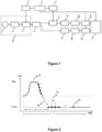
- Figure 1 shows a system architecture for pulsed power measurement with high dynamic range and high speed.
- a measurement apparatus allowing to determine the power levels of pulsed optical signals in conduction and cut-off states with high dynamic range and high speed, wherein said apparatus comprises; a pulsed power signal generator (123) generating pulses having synchronous trigger signals and comprising at least one signal source (1) which generates continuous signals, at least one power amplifier (2) amplifies signals generated in said signal source (1), at least one amplitude modulator-I (3) to generate pulses from said continuous signals, at least one power divider unit (5) connected to the modulator-I's (3) output and divides the signals coming from the modulator-I (3) to parts as a low power part and a high power part, at least one driver unit (4) to drive the modulator-I (3), at least one receiver-I (9a) connected to the low power output of the power divider unit (5) and measures the high power part (i.e.
- the pulsed optical signal at least one low pass filter-II (10b) connected to the receiver-II (9b), at least one analog-digital converter-II (11b) for digitizing signals taken from the low pass filter-II (10), at least one data processing and monitoring unit (12) forming a pulse profile by processing and respectively combining signals which digitally coming from the analog digital converter-I (11a) and analog digital converter-II (11b), at least one driver-I (4) amplifying pulses needed by the modulator-I (3), at least one driver-II (7) amplifying pulses needed by the modulator-II (8), at least one timing unit (6) connected to the driver-I (4) and driver-II (7) for controlling the modulator-I (3) and the modulator-II (8) by making modulator-II (8) to enter into cut-off mode when the modulator-I (3) is in conduction mode and making the modulator-II (8) to enter into the conduction mode -I when the modulator-I (3) is
- the invention relates to the apparatus as described above and a method that can be run on this apparatus, preferably can be employed with an optical system.
- a laser signal source, an optical power amplifier, modulators, coupler and optical receivers are used instead of respectively signal source (1), power amplifier (2), modulator-I (3), modulator-II (8), power divider (5) and receiver-I (9a), receiver-II(9b).
- the optical signal generated in a laser signal source is amplified by an optical power amplifier (2). Obtained high power continuous wave optical signal is transmitted to the modulator-I (3) and amplitude modulation is applied. Depending on the conduction/cut-off durations of the modulation, a pulsed optical signal is generated in the desired form.
- the high power and fast driving pulses required by the modulator-I (3) are supplied by the driver-I (4).
- the pulse width, period and the starting time are determined by the timing unit (6).
- Generated pulsed optical signal is branched into two signals with different power levels by means of the coupler. The optical signals are going to be processed as two signal like high power and low power part.
- the low power part of the optical signal is transmitted to the data processing and monitoring unit (12) after digitized by the optical receiver-I (9a), low-pass filter-I (10a) and analog-digital converter-I (11a) whereas the high power part of the optical signal is transmitted to the data processing and monitoring unit (12) after digitized by modulator-II (8), optical receiver-II (9b), low-pass filter-II (10b) and analog-digital converter-II (11b).
- the high power and fast driving pulses required by the modulator-II (8) are supplied by the driver-II (7).
- the pulse width, period and the starting time are determined again by the timing unit (6).
- the main challenge about pulsed power measurement is high dynamic range of two different power levels (Ppeak, Pmin) whereas, the measured pulse width is narrow in the order of nanoseconds.
- the power measurement should be made for each pulse period, meanly high speed and high dynamic range requirement must be met at the same time.
- BW recovery bandwidth
- the minimum power level (Pmin) that can be measured increases in proportion to the square root of the measurement bandwidth. This also means that, the dynamic range of the detector is reduced.
- receiver-I (9a) and receiver-II (9b) are used for high-speed and low-noise measurement to eliminate said constraint.
- One of these receivers measures the high speed/high power pulse part (conduction state power) of the optical signal, while the other receiver measures the low power/long duration part of the optical signal.
- the receiver-I (9a) and receiver-II (9b) differ in bandwidth or integration time and power levels they are optimized to measure as well. Using different level of integration time and sensitivity receivers is possible because of the nature of the low duty cycle pulse signal which has off duration much longer than on duration and conduction state power is much higher than the cut off state power.
- the width of the measured optical pulse is in the order of 100 nanoseconds
- the time of the relaxing (cut off) after the pulse may be in the order of 500 microseconds.
- optical receiver, photodiode and power meters are the devices used to convert optical power to electrical signal in general sense. But there is some differences such as; photodetector is bare form of optical to electrical signal conversion, optical receiver is one with additional circuitry like transimpedance amplification of photodiode output current and some additional filtering and biasing.
- Power meter is a device directly converting optical signal to power reading.
- the low-pass filter-I (10a) and the low-pass filter (10b) (II) are used for band limiting and anti-aliasing purposes.
- the power distribution at the outputs of the power divider unit (5) is branched into as high-power and low-power parts asymmetrically.
- the low power output part is transmitted directly to the optical receiver-I (9a) and the minimally attenuated high power output part is transmitted to the modulator-II (8).
- the trigger signals that drive modulator-II (8) into on/off states is shown.
- the trigger signal of modulators (3, 8) for conduction state (17) and the trigger signal of modulators for cut-off state (18) are binary level signal.
- the trigger signal may contain high frequency RF carrier.
- the conduction / cut-off states generated by the modulator-II (8) is in synchronization with conduction / cut-off states of the modulator-I (3) which responsible for generating pulsed signal.
- the scope of this synchronization is to operate the two modulators (3, 8) at the same frequency and to compensate for the delays along the signal path appropriately.
- the timing unit (6) manage this function.
- the reason of why the modulator-II (8) is driven into the cut-off states in when the modulator-I (3) is in conduction state is to prevent transmitting of the conduction state power of pulsed power signal generator (123) to the high sensitivity optical receiver-II (9b) and the result of measurement thus, allowing only the measurement of minimum power level (Pmin).
- the high power part of the measured pulse is isolated electronically thus, the measurement of the minimum power level (Pmin) can be performed with low power/high sensitivity optical receiver-I (9a) and in longer integration time (T >> ⁇ ).
- the minimum power value level(Pmin) can be measured with sufficient accuracy depending on the on/off isolation level of the modulator-II (8).
- the modulator-II (8) does not suppress the peak power level (Ppeak) enough, the leaked power during ⁇ came from high power part will affect the measurement of the minimum power level (Pmin). For example, if the Ppeak / Pmin ratio of the optical signal to be measured is 120 dB, the isolation required by the modulator-II (8) should be greater than 120 dB. As the isolation level increases, the error of measuring the Pmin value is reduced. In case of using acousto-optic modulator (AOM) as modulator-II (8), when the commercial products are examined, the typical value of the isolation level that can be achieved with a single device is 60 dB. These modules can be connected in series to achieve isolation values of 120 dB and higher.
- AOM acousto-optic modulator
- Cut-off time for the modulator-II (8) is ⁇ , and the conduction time for the modulator-II (8) can be supposed to be the measurement time window (14) at least and up to (T- ⁇ ).
- the conduction time for the modulator-II (8) can be supposed to be the measurement time window (14) at least and up to (T- ⁇ ).
- receivers (9a, 9b) with low noise equivalent power rated photodiodes and long integration time. For example, if the pulse width is 100 nanosecond and the pulse repetition period is 1 millisecond, the signal is at 0.01% peak power level (Ppeak) and 99.99% at minimum power level (Pmin) values. The time available for measuring the minimum power level (Pmin) of the signal (0,999ms) is much longer compared to the pulse time (100 ns).
- the minimum power level (Pmin) that the optical receiver-II (9b) can measure is reduced.
- the cut-off period can be used completely after the pulse also, a narrower measurement window (14) can be used.
- a narrow measurement window (14) can be used to observe how the minimum power level (Pmin) changes over multiple pulse repetition period at a specific time instant.
- T is the pulse period
- ⁇ is the pulse width
- ⁇ m is the measurement window (14) duration
- N T ⁇ ⁇ ⁇ m where N is the number of samples can be acquired separately, thus measurement time resolution of minimum power level (Pmin).
- Pmin P ave ⁇ T ⁇ m
- P min P ave ⁇ T ⁇ m
- P min P ave ⁇ T ⁇ m
- the photodiode or optical receiver (9a, 9b) is used instead of power meter, direct value of Pmin can be read but in the expense of higher measurable minimum power.
- Commercial power meter has much narrow bandwidth enabling lower signal measurement and outputs average power.
- the measured points are digitized with the analog-to-digital converter-II (1 1b) to create a pulse profile of minimum power level (Pmin) and can be displayed to the user graphically as in figure 2 .
- the integration time in the relevant measurement window (14) can be extended by employing repetitive sampling at the same time instant which enables lower level power measurement.
- the optical receiver-I (9a) is selected as high-speed/wideband, in particular for measurement during the pulse time ( ⁇ ) and should withstands pulse peak power.
- Analog-digital converter-I (11a) samples at the output of the optical receiver-I (9a) provides direct pulse profile of high power part of the optical signal. After acquisition of samples from two branches, the whole data is transferred to the data processing and monitoring unit (12) where data samples are combined in time respectively so that complete pulse profile is formed.
- Power division ratio of the power divider unit (5) is selected by considering the peak power level (Ppeak) of the pulse and the power limits of the optical receivers used for measurement. For example, if the peak power level (Ppeak) of the optical pulse is +30 dBm and the maximum power that the optical receiver-I (9a) which is connected with the low power path can with stand is +10 dBm, the power divider unit (5) must provide 20 dB power attenuation at least in related arm.
- optical receiver-II (9a) Assuming that the maximum input power level at which optical receiver-I (9a) works approximately is +10 dBm, the minimum measurable input power of optical receiver-II (9b) is -110 dBm@100us, if input pulse with peak power of +30dBm to be measured, 140 dB (+30dBm-(-110dBm)) dynamic range can be achieved thanks to the invention.
- the pulses with a higher peak value can be measured by increasing power division ratio of the power divider unit (5).
- the power divider unit (5) and the modulator-II (8) must be capable of withstanding high input power levels (> +30 dBm).
- the blind region (16) may be interpolated approximately from known data points around it.
- Fiber optic distributed sensor systems are able to detect vibration, strain, temperature and their position along the fiber optic cable by interrogating the cable with optical pulses in kilometers range.
- mentioned pulses can be generated by means of the laser signal source (1), the optic power amplifier (2), the modulator-I (3) which are the elements of the pulsed power signal generator (123), the driver-I (4) and the timing unit (6) of the system shown in figure 1 .
- the stability of generated pulses in terms of width, amplitude and period is critical to the system performance of the fiber optic sensor. These parameters have direct effects on the noise level of the fiber optic sensor. Therefore, the accurate power measurement and profiling of the optical pulse that fiber optic sensor sent to the fiber cable is extremely important for evaluating and improving system performance.
- the pulse form (13) which is expected to be rectangular in the ideal case, may take a different shape as seen in figure 2 in consequence of some effects arise from the laser signal source (1), the optical power amplifier (2), the modulator-I (3) and the driver-I (4). Also, some additional spurious signals (15) may appear due to electromagnetic coupling within the system.
- the measurement of the pulse form (13) resulting from the combination of different effects during system operation is very helpful to detect and remove errors within the system.
- Using commercial power meters one can only measure the steady state power levels of the system output power so cannot cover dynamic behavior which is critical to find sources of some anomalies within the system.
- the invention is capable of performing measurement of pulse power and profiling dynamically as needed. Consequently, the invention is eliminating shortcomings of commercial power measurement.
- the power measurement technique of the invention is not useful for only measuring power of optical laser pulses, mentioned technique can also be used for power measurement in any band across the electromagnetic spectrum in case of providing suitable sub-units.
- a RF oscillator instead of the signal source (1)
- a RF power amplifier instead of the optical power amplifier (2)
- RF switches instead of the modulators (3,8)
- a medium class RF power amplifier instead of the drivers (4, 7)
- a RF coupler and a receivers instead of the power divider unit (5) and optical receivers (9a, 9b)
- the other elements of the system (6, 10.a, 10.b, 11.a, 11.b and 12) are kept same.
Landscapes
- Physics & Mathematics (AREA)
- General Physics & Mathematics (AREA)
- Engineering & Computer Science (AREA)
- Power Engineering (AREA)
- Spectroscopy & Molecular Physics (AREA)
- Photometry And Measurement Of Optical Pulse Characteristics (AREA)
Claims (3)
- Appareil de mesure permettant de déterminer les niveaux de puissance de signaux optiques pulsés
dans des états de conduction et de coupure avec une plage dynamique élevée et une vitesse élevée comprenant ;• au moins un générateur de signaux de puissance pulsés (123) générant des impulsions optiques comportant des signaux de déclenchement synchrones et comprenant ; au moins une source de signaux optiques (1) générant des signaux optiques continus, au moins un amplificateur de puissance (2) amplifiant des signaux générés dans ladite source de signaux optiques (1), au moins un modulateur-1 d'amplitude (3) générant un signal optique pulsé à partir desdits signaux optiques continus,• au moins une unité diviseuse de puissance (5) connectée à la sortie du modulateur-1 (3), comprenant une sortie faible puissance et une sortie haute puissance, et configurée pour diviser le signal optique pulsé provenant du modulateur-1 (3) en parties en tant que partie faible puissance et partie haute puissance,• au moins un récepteur-I (9a) connecté à la sortie faible puissance de l'unité diviseuse de puissance (5) et configuré pour mesurer la partie faible puissance du signal optique pulsé,• au moins un filtre-1 passe-bas (10a) connecté au récepteur-I (9a) et configuré pour effectuer une limitation de bande et un antirepliement,• au moins un convertisseur-I analogique-numérique (11a) configuré pour numériser les signaux issus du filtre-1 passe-bas (10a),- au moins un modulateur-II (8) connecté à la sortie haute puissance de l'unité diviseuse de puissance (5) et configuré pour empêcher la partie haute puissance du signal optique pulsé d'atteindre au moins un pilote-II (7) en entrant dans le mode coupure lorsque le modulateur-1 (3) est en mode conduction et en entrant dans le mode conduction lorsque le modulateur-1 (3) est en mode coupure,• au moins un récepteur-II (9b) connecté à la sortie haute puissance de l'unité diviseuse de puissance (5) et configuré pour mesurer la partie haute puissance du signal optique pulsé,• au moins un filtre-1 passe-bas (10b) connecté au récepteur-II (9b) et configuré pour effectuer une limitation de bande et un antirepliement,• au moins un convertisseur-II analogique-numérique (11b) configuré pour numériser les signaux provenant du filtre-1 passe-bas (10b),• au moins une unité de traitement de données et de surveillance (12) configurée pour former un profil d'impulsion en traitant et en combinant respectivement numériquement des signaux provenant du convertisseur-1 analogique-numérique (11a) et du convertisseur-II analogique-numérique (11b) ;• au moins un pilote-1 (4) configuré pour amplifier les impulsions nécessaires au modulateur-1 (3),• le au moins un pilote-II (7) configuré pour amplifier les impulsions nécessaires au modulateur-II (8) et• au moins une unité de synchronisation (6) connectée audit au moins un pilote-I (4) et audit au moins un pilote-II (7) etconfiguré pour commander le modulateur-1 (3) et le modulateur-II (8) en faisant entrer le modulateur-II (8) dans l'état de coupure lorsque le modulateur-1 (3) est en mode conduction et en faisant entrer le modulateur-II (8) dans le mode conduction lorsque le modulateur-1 (3) est en mode coupure de façon à faire fonctionner le modulateur-1 et le modulateur-II (3, 8) de manière synchronisée. - Appareil de mesure selon la revendication 1, caractérisé par l'unité de synchronisation (6) configurée pour régler le retard entre les signaux de déclenchement afin de compenser les temps de propagation de signal le long du trajet de signal.
- Appareil de mesure selon la revendication 1 ou 2, caractérisé par l'unité diviseuse de puissance (5) configurée pour déterminer un rapport de division de puissance en considérant un niveau de puissance de crête d'impulsion et des limites de puissance du récepteur-I (9a) et du récepteur-II (9b).
Applications Claiming Priority (1)
| Application Number | Priority Date | Filing Date | Title |
|---|---|---|---|
| PCT/TR2018/050886 WO2020139207A1 (fr) | 2018-12-25 | 2018-12-25 | Procédé et appareil de mesure de puissance pulsée |
Publications (3)
| Publication Number | Publication Date |
|---|---|
| EP3903078A1 EP3903078A1 (fr) | 2021-11-03 |
| EP3903078B1 true EP3903078B1 (fr) | 2024-04-17 |
| EP3903078C0 EP3903078C0 (fr) | 2024-04-17 |
Family
ID=65269027
Family Applications (1)
| Application Number | Title | Priority Date | Filing Date |
|---|---|---|---|
| EP18842677.9A Active EP3903078B1 (fr) | 2018-12-25 | 2018-12-25 | Procédé et appareil de mesure de puissance pulsée |
Country Status (3)
| Country | Link |
|---|---|
| US (1) | US11782078B2 (fr) |
| EP (1) | EP3903078B1 (fr) |
| WO (1) | WO2020139207A1 (fr) |
Families Citing this family (3)
| Publication number | Priority date | Publication date | Assignee | Title |
|---|---|---|---|---|
| US11609386B2 (en) * | 2019-06-25 | 2023-03-21 | Panduit Corp. | System and method for insertion loss evaluation of connectors |
| WO2023043498A1 (fr) * | 2021-09-16 | 2023-03-23 | Viasat, Inc. | Procédé et appareil de détection de puissance dans un émetteur radiofréquence |
| CN115655491A (zh) * | 2022-09-28 | 2023-01-31 | 河北汉光重工有限责任公司 | 一种纳秒级脉冲积分式测量装置 |
Family Cites Families (4)
| Publication number | Priority date | Publication date | Assignee | Title |
|---|---|---|---|---|
| US5491548A (en) | 1994-03-18 | 1996-02-13 | Tektronix, Inc. | Optical signal measurement instrument and wide dynamic range optical receiver for use therein |
| US6784987B2 (en) | 2001-01-19 | 2004-08-31 | Dbm Optics, Incorporated | Non-linear ranging to control linear ranging measurement device |
| US7103077B2 (en) * | 2004-04-29 | 2006-09-05 | 20/10 Perfect Vision Optische Geraete Gmbh | System and method for measuring and controlling an energy of an ultra-short pulse of a laser beam |
| US9395407B2 (en) * | 2014-04-03 | 2016-07-19 | X-Com Systems, Llc | Enhanced dynamic range RF pulse measurement system |
-
2018
- 2018-12-25 WO PCT/TR2018/050886 patent/WO2020139207A1/fr not_active Ceased
- 2018-12-25 EP EP18842677.9A patent/EP3903078B1/fr active Active
- 2018-12-25 US US17/312,430 patent/US11782078B2/en active Active
Also Published As
| Publication number | Publication date |
|---|---|
| EP3903078A1 (fr) | 2021-11-03 |
| WO2020139207A1 (fr) | 2020-07-02 |
| US11782078B2 (en) | 2023-10-10 |
| EP3903078C0 (fr) | 2024-04-17 |
| US20220018883A1 (en) | 2022-01-20 |
Similar Documents
| Publication | Publication Date | Title |
|---|---|---|
| CA2515705C (fr) | Procede et dispositif de production et d'emission d'impulsions optiques de haute energie pour mesures de grandes distances | |
| CN103401606B (zh) | 一种基于探测频率编码的相干光时域反射仪 | |
| JP7029620B2 (ja) | パルス干渉ドップラー風計測レーザーレーダー及び風計測方法 | |
| CN108663138B (zh) | 一种分布式光纤温度及振动的传感系统及方法 | |
| CN113810098B (zh) | 一种基于双边带啁啾脉冲调制的光时域反射计 | |
| EP3903078B1 (fr) | Procédé et appareil de mesure de puissance pulsée | |
| JP2012159387A (ja) | 光ファイバ特性測定装置及び方法 | |
| US10816368B2 (en) | Method and system for high sensitivity in distributed fiber sensing applications | |
| EP3848676B1 (fr) | Appareil de mesure de caractéristique de fibre optique et procédé de mesure de caractéristique de fibre optique | |
| US11385127B2 (en) | Optical frequency multiplexing coherent OTDR, testing method, signal processing device, and program | |
| US20180340860A1 (en) | Optical Time Domain Reflectometer with High Resolution and High Sensitivity | |
| JP3094917B2 (ja) | 光ファイバ歪み測定装置 | |
| CN117968823B (zh) | 分布式光纤声音传感装置及声音探测方法 | |
| JPH05240699A (ja) | 後方散乱光の測定装置 | |
| JP2014122802A (ja) | 光パルス試験装置及び光パルス試験方法 | |
| US10784958B2 (en) | Method and device of determining a time-of-flight of an optical signal between a starting point of an optical path and a reflection point within the optical path | |
| CN113607277B (zh) | 一种窄线宽激光器线宽测量系统的解调方法 | |
| JP2013152182A (ja) | ブリルアン光パルス試験器 | |
| JP6847325B1 (ja) | コヒーレントライダ装置 | |
| US6417926B1 (en) | Wavelength measuring system | |
| JP2009281813A (ja) | 光ファイバ測定装置 | |
| JPH05322695A (ja) | 光パルス試験器 | |
| JP7351365B1 (ja) | 光ファイバセンサ及びブリルアン周波数シフト測定方法 | |
| CN111896141A (zh) | 一种测温系统与提高系统性能的方法和系统应用方法 | |
| CN113916498A (zh) | 一种波分复用非相干光频域反射光纤质量检测装置及方法 |
Legal Events
| Date | Code | Title | Description |
|---|---|---|---|
| STAA | Information on the status of an ep patent application or granted ep patent |
Free format text: STATUS: UNKNOWN |
|
| STAA | Information on the status of an ep patent application or granted ep patent |
Free format text: STATUS: THE INTERNATIONAL PUBLICATION HAS BEEN MADE |
|
| PUAI | Public reference made under article 153(3) epc to a published international application that has entered the european phase |
Free format text: ORIGINAL CODE: 0009012 |
|
| STAA | Information on the status of an ep patent application or granted ep patent |
Free format text: STATUS: REQUEST FOR EXAMINATION WAS MADE |
|
| 17P | Request for examination filed |
Effective date: 20210617 |
|
| AK | Designated contracting states |
Kind code of ref document: A1 Designated state(s): AL AT BE BG CH CY CZ DE DK EE ES FI FR GB GR HR HU IE IS IT LI LT LU LV MC MK MT NL NO PL PT RO RS SE SI SK SM TR |
|
| DAV | Request for validation of the european patent (deleted) | ||
| DAX | Request for extension of the european patent (deleted) | ||
| STAA | Information on the status of an ep patent application or granted ep patent |
Free format text: STATUS: EXAMINATION IS IN PROGRESS |
|
| 17Q | First examination report despatched |
Effective date: 20230306 |
|
| 17Q | First examination report despatched |
Effective date: 20230314 |
|
| P01 | Opt-out of the competence of the unified patent court (upc) registered |
Effective date: 20230529 |
|
| GRAP | Despatch of communication of intention to grant a patent |
Free format text: ORIGINAL CODE: EPIDOSNIGR1 |
|
| STAA | Information on the status of an ep patent application or granted ep patent |
Free format text: STATUS: GRANT OF PATENT IS INTENDED |
|
| INTG | Intention to grant announced |
Effective date: 20231212 |
|
| GRAS | Grant fee paid |
Free format text: ORIGINAL CODE: EPIDOSNIGR3 |
|
| GRAA | (expected) grant |
Free format text: ORIGINAL CODE: 0009210 |
|
| STAA | Information on the status of an ep patent application or granted ep patent |
Free format text: STATUS: THE PATENT HAS BEEN GRANTED |
|
| AK | Designated contracting states |
Kind code of ref document: B1 Designated state(s): AL AT BE BG CH CY CZ DE DK EE ES FI FR GB GR HR HU IE IS IT LI LT LU LV MC MK MT NL NO PL PT RO RS SE SI SK SM TR |
|
| REG | Reference to a national code |
Ref country code: GB Ref legal event code: FG4D |
|
| REG | Reference to a national code |
Ref country code: CH Ref legal event code: EP |
|
| REG | Reference to a national code |
Ref country code: DE Ref legal event code: R096 Ref document number: 602018068300 Country of ref document: DE |
|
| REG | Reference to a national code |
Ref country code: IE Ref legal event code: FG4D |
|
| U01 | Request for unitary effect filed |
Effective date: 20240514 |
|
| P04 | Withdrawal of opt-out of the competence of the unified patent court (upc) registered |
Effective date: 20240518 |
|
| U07 | Unitary effect registered |
Designated state(s): AT BE BG DE DK EE FI FR IT LT LU LV MT NL PT SE SI Effective date: 20240523 |
|
| PG25 | Lapsed in a contracting state [announced via postgrant information from national office to epo] |
Ref country code: IS Free format text: LAPSE BECAUSE OF FAILURE TO SUBMIT A TRANSLATION OF THE DESCRIPTION OR TO PAY THE FEE WITHIN THE PRESCRIBED TIME-LIMIT Effective date: 20240817 |
|
| PG25 | Lapsed in a contracting state [announced via postgrant information from national office to epo] |
Ref country code: HR Free format text: LAPSE BECAUSE OF FAILURE TO SUBMIT A TRANSLATION OF THE DESCRIPTION OR TO PAY THE FEE WITHIN THE PRESCRIBED TIME-LIMIT Effective date: 20240417 |
|
| PG25 | Lapsed in a contracting state [announced via postgrant information from national office to epo] |
Ref country code: GR Free format text: LAPSE BECAUSE OF FAILURE TO SUBMIT A TRANSLATION OF THE DESCRIPTION OR TO PAY THE FEE WITHIN THE PRESCRIBED TIME-LIMIT Effective date: 20240718 |
|
| PG25 | Lapsed in a contracting state [announced via postgrant information from national office to epo] |
Ref country code: ES Free format text: LAPSE BECAUSE OF FAILURE TO SUBMIT A TRANSLATION OF THE DESCRIPTION OR TO PAY THE FEE WITHIN THE PRESCRIBED TIME-LIMIT Effective date: 20240417 |
|
| PG25 | Lapsed in a contracting state [announced via postgrant information from national office to epo] |
Ref country code: PL Free format text: LAPSE BECAUSE OF FAILURE TO SUBMIT A TRANSLATION OF THE DESCRIPTION OR TO PAY THE FEE WITHIN THE PRESCRIBED TIME-LIMIT Effective date: 20240417 |
|
| PG25 | Lapsed in a contracting state [announced via postgrant information from national office to epo] |
Ref country code: PL Free format text: LAPSE BECAUSE OF FAILURE TO SUBMIT A TRANSLATION OF THE DESCRIPTION OR TO PAY THE FEE WITHIN THE PRESCRIBED TIME-LIMIT Effective date: 20240417 Ref country code: NO Free format text: LAPSE BECAUSE OF FAILURE TO SUBMIT A TRANSLATION OF THE DESCRIPTION OR TO PAY THE FEE WITHIN THE PRESCRIBED TIME-LIMIT Effective date: 20240717 Ref country code: IS Free format text: LAPSE BECAUSE OF FAILURE TO SUBMIT A TRANSLATION OF THE DESCRIPTION OR TO PAY THE FEE WITHIN THE PRESCRIBED TIME-LIMIT Effective date: 20240817 Ref country code: HR Free format text: LAPSE BECAUSE OF FAILURE TO SUBMIT A TRANSLATION OF THE DESCRIPTION OR TO PAY THE FEE WITHIN THE PRESCRIBED TIME-LIMIT Effective date: 20240417 Ref country code: GR Free format text: LAPSE BECAUSE OF FAILURE TO SUBMIT A TRANSLATION OF THE DESCRIPTION OR TO PAY THE FEE WITHIN THE PRESCRIBED TIME-LIMIT Effective date: 20240718 Ref country code: ES Free format text: LAPSE BECAUSE OF FAILURE TO SUBMIT A TRANSLATION OF THE DESCRIPTION OR TO PAY THE FEE WITHIN THE PRESCRIBED TIME-LIMIT Effective date: 20240417 Ref country code: RS Free format text: LAPSE BECAUSE OF FAILURE TO SUBMIT A TRANSLATION OF THE DESCRIPTION OR TO PAY THE FEE WITHIN THE PRESCRIBED TIME-LIMIT Effective date: 20240717 |
|
| P05 | Withdrawal of opt-out of the competence of the unified patent court (upc) changed |
Free format text: CASE NUMBER: APP_28472/2024 Effective date: 20240523 |
|
| REG | Reference to a national code |
Ref country code: DE Ref legal event code: R097 Ref document number: 602018068300 Country of ref document: DE |
|
| PG25 | Lapsed in a contracting state [announced via postgrant information from national office to epo] |
Ref country code: CZ Free format text: LAPSE BECAUSE OF FAILURE TO SUBMIT A TRANSLATION OF THE DESCRIPTION OR TO PAY THE FEE WITHIN THE PRESCRIBED TIME-LIMIT Effective date: 20240417 |
|
| PG25 | Lapsed in a contracting state [announced via postgrant information from national office to epo] |
Ref country code: SK Free format text: LAPSE BECAUSE OF FAILURE TO SUBMIT A TRANSLATION OF THE DESCRIPTION OR TO PAY THE FEE WITHIN THE PRESCRIBED TIME-LIMIT Effective date: 20240417 Ref country code: RO Free format text: LAPSE BECAUSE OF FAILURE TO SUBMIT A TRANSLATION OF THE DESCRIPTION OR TO PAY THE FEE WITHIN THE PRESCRIBED TIME-LIMIT Effective date: 20240417 |
|
| PG25 | Lapsed in a contracting state [announced via postgrant information from national office to epo] |
Ref country code: SM Free format text: LAPSE BECAUSE OF FAILURE TO SUBMIT A TRANSLATION OF THE DESCRIPTION OR TO PAY THE FEE WITHIN THE PRESCRIBED TIME-LIMIT Effective date: 20240417 |
|
| U20 | Renewal fee for the european patent with unitary effect paid |
Year of fee payment: 7 Effective date: 20241220 |
|
| PG25 | Lapsed in a contracting state [announced via postgrant information from national office to epo] |
Ref country code: SM Free format text: LAPSE BECAUSE OF FAILURE TO SUBMIT A TRANSLATION OF THE DESCRIPTION OR TO PAY THE FEE WITHIN THE PRESCRIBED TIME-LIMIT Effective date: 20240417 Ref country code: SK Free format text: LAPSE BECAUSE OF FAILURE TO SUBMIT A TRANSLATION OF THE DESCRIPTION OR TO PAY THE FEE WITHIN THE PRESCRIBED TIME-LIMIT Effective date: 20240417 Ref country code: RO Free format text: LAPSE BECAUSE OF FAILURE TO SUBMIT A TRANSLATION OF THE DESCRIPTION OR TO PAY THE FEE WITHIN THE PRESCRIBED TIME-LIMIT Effective date: 20240417 Ref country code: CZ Free format text: LAPSE BECAUSE OF FAILURE TO SUBMIT A TRANSLATION OF THE DESCRIPTION OR TO PAY THE FEE WITHIN THE PRESCRIBED TIME-LIMIT Effective date: 20240417 |
|
| PLBE | No opposition filed within time limit |
Free format text: ORIGINAL CODE: 0009261 |
|
| STAA | Information on the status of an ep patent application or granted ep patent |
Free format text: STATUS: NO OPPOSITION FILED WITHIN TIME LIMIT |
|
| 26N | No opposition filed |
Effective date: 20250120 |
|
| PG25 | Lapsed in a contracting state [announced via postgrant information from national office to epo] |
Ref country code: MC Free format text: LAPSE BECAUSE OF FAILURE TO SUBMIT A TRANSLATION OF THE DESCRIPTION OR TO PAY THE FEE WITHIN THE PRESCRIBED TIME-LIMIT Effective date: 20240417 |
|
| REG | Reference to a national code |
Ref country code: CH Ref legal event code: PL |
|
| GBPC | Gb: european patent ceased through non-payment of renewal fee |
Effective date: 20241225 |
|
| PG25 | Lapsed in a contracting state [announced via postgrant information from national office to epo] |
Ref country code: GB Free format text: LAPSE BECAUSE OF NON-PAYMENT OF DUE FEES Effective date: 20241225 |
|
| PG25 | Lapsed in a contracting state [announced via postgrant information from national office to epo] |
Ref country code: CH Free format text: LAPSE BECAUSE OF NON-PAYMENT OF DUE FEES Effective date: 20241231 |
|
| PG25 | Lapsed in a contracting state [announced via postgrant information from national office to epo] |
Ref country code: IE Free format text: LAPSE BECAUSE OF NON-PAYMENT OF DUE FEES Effective date: 20241225 |
|
| U20 | Renewal fee for the european patent with unitary effect paid |
Year of fee payment: 8 Effective date: 20251224 |