EP3912301B1 - Procédé d'émission de signal de référence de sondage et dispositif électronique pour cela - Google Patents
Procédé d'émission de signal de référence de sondage et dispositif électronique pour cela Download PDFInfo
- Publication number
- EP3912301B1 EP3912301B1 EP20781787.5A EP20781787A EP3912301B1 EP 3912301 B1 EP3912301 B1 EP 3912301B1 EP 20781787 A EP20781787 A EP 20781787A EP 3912301 B1 EP3912301 B1 EP 3912301B1
- Authority
- EP
- European Patent Office
- Prior art keywords
- signal
- antenna
- electronic device
- strength
- antennas
- Prior art date
- Legal status (The legal status is an assumption and is not a legal conclusion. Google has not performed a legal analysis and makes no representation as to the accuracy of the status listed.)
- Active
Links
Images




Classifications
-
- H—ELECTRICITY
- H04—ELECTRIC COMMUNICATION TECHNIQUE
- H04B—TRANSMISSION
- H04B7/00—Radio transmission systems, i.e. using radiation field
- H04B7/02—Diversity systems; Multi-antenna system, i.e. transmission or reception using multiple antennas
- H04B7/04—Diversity systems; Multi-antenna system, i.e. transmission or reception using multiple antennas using two or more spaced independent antennas
- H04B7/06—Diversity systems; Multi-antenna system, i.e. transmission or reception using multiple antennas using two or more spaced independent antennas at the transmitting station
- H04B7/0602—Diversity systems; Multi-antenna system, i.e. transmission or reception using multiple antennas using two or more spaced independent antennas at the transmitting station using antenna switching
- H04B7/0608—Antenna selection according to transmission parameters
-
- H—ELECTRICITY
- H04—ELECTRIC COMMUNICATION TECHNIQUE
- H04L—TRANSMISSION OF DIGITAL INFORMATION, e.g. TELEGRAPHIC COMMUNICATION
- H04L5/00—Arrangements affording multiple use of the transmission path
- H04L5/003—Arrangements for allocating sub-channels of the transmission path
- H04L5/0032—Distributed allocation, i.e. involving a plurality of allocating devices, each making partial allocation
-
- H—ELECTRICITY
- H04—ELECTRIC COMMUNICATION TECHNIQUE
- H04L—TRANSMISSION OF DIGITAL INFORMATION, e.g. TELEGRAPHIC COMMUNICATION
- H04L5/00—Arrangements affording multiple use of the transmission path
- H04L5/003—Arrangements for allocating sub-channels of the transmission path
- H04L5/0048—Allocation of pilot signals, i.e. of signals known to the receiver
- H04L5/0051—Allocation of pilot signals, i.e. of signals known to the receiver of dedicated pilots, i.e. pilots destined for a single user or terminal
-
- H—ELECTRICITY
- H04—ELECTRIC COMMUNICATION TECHNIQUE
- H04B—TRANSMISSION
- H04B17/00—Monitoring; Testing
- H04B17/10—Monitoring; Testing of transmitters
- H04B17/101—Monitoring; Testing of transmitters for measurement of specific parameters of the transmitter or components thereof
- H04B17/103—Reflected power, e.g. return loss
-
- H—ELECTRICITY
- H04—ELECTRIC COMMUNICATION TECHNIQUE
- H04B—TRANSMISSION
- H04B17/00—Monitoring; Testing
- H04B17/30—Monitoring; Testing of propagation channels
- H04B17/309—Measuring or estimating channel quality parameters
- H04B17/318—Received signal strength
- H04B17/328—Reference signal received power [RSRP]; Reference signal received quality [RSRQ]
-
- H—ELECTRICITY
- H04—ELECTRIC COMMUNICATION TECHNIQUE
- H04B—TRANSMISSION
- H04B7/00—Radio transmission systems, i.e. using radiation field
- H04B7/02—Diversity systems; Multi-antenna system, i.e. transmission or reception using multiple antennas
- H04B7/04—Diversity systems; Multi-antenna system, i.e. transmission or reception using multiple antennas using two or more spaced independent antennas
- H04B7/0404—Diversity systems; Multi-antenna system, i.e. transmission or reception using multiple antennas using two or more spaced independent antennas the mobile station comprising multiple antennas, e.g. to provide uplink diversity
-
- H—ELECTRICITY
- H04—ELECTRIC COMMUNICATION TECHNIQUE
- H04B—TRANSMISSION
- H04B7/00—Radio transmission systems, i.e. using radiation field
- H04B7/02—Diversity systems; Multi-antenna system, i.e. transmission or reception using multiple antennas
- H04B7/04—Diversity systems; Multi-antenna system, i.e. transmission or reception using multiple antennas using two or more spaced independent antennas
- H04B7/0413—MIMO systems
-
- H—ELECTRICITY
- H04—ELECTRIC COMMUNICATION TECHNIQUE
- H04B—TRANSMISSION
- H04B7/00—Radio transmission systems, i.e. using radiation field
- H04B7/02—Diversity systems; Multi-antenna system, i.e. transmission or reception using multiple antennas
- H04B7/04—Diversity systems; Multi-antenna system, i.e. transmission or reception using multiple antennas using two or more spaced independent antennas
- H04B7/06—Diversity systems; Multi-antenna system, i.e. transmission or reception using multiple antennas using two or more spaced independent antennas at the transmitting station
- H04B7/0602—Diversity systems; Multi-antenna system, i.e. transmission or reception using multiple antennas using two or more spaced independent antennas at the transmitting station using antenna switching
- H04B7/0608—Antenna selection according to transmission parameters
- H04B7/061—Antenna selection according to transmission parameters using feedback from receiving side
-
- H—ELECTRICITY
- H04—ELECTRIC COMMUNICATION TECHNIQUE
- H04B—TRANSMISSION
- H04B7/00—Radio transmission systems, i.e. using radiation field
- H04B7/02—Diversity systems; Multi-antenna system, i.e. transmission or reception using multiple antennas
- H04B7/04—Diversity systems; Multi-antenna system, i.e. transmission or reception using multiple antennas using two or more spaced independent antennas
- H04B7/06—Diversity systems; Multi-antenna system, i.e. transmission or reception using multiple antennas using two or more spaced independent antennas at the transmitting station
- H04B7/0686—Hybrid systems, i.e. switching and simultaneous transmission
- H04B7/0691—Hybrid systems, i.e. switching and simultaneous transmission using subgroups of transmit antennas
-
- H—ELECTRICITY
- H04—ELECTRIC COMMUNICATION TECHNIQUE
- H04L—TRANSMISSION OF DIGITAL INFORMATION, e.g. TELEGRAPHIC COMMUNICATION
- H04L5/00—Arrangements affording multiple use of the transmission path
- H04L5/003—Arrangements for allocating sub-channels of the transmission path
- H04L5/0048—Allocation of pilot signals, i.e. of signals known to the receiver
-
- H—ELECTRICITY
- H04—ELECTRIC COMMUNICATION TECHNIQUE
- H04L—TRANSMISSION OF DIGITAL INFORMATION, e.g. TELEGRAPHIC COMMUNICATION
- H04L5/00—Arrangements affording multiple use of the transmission path
- H04L5/003—Arrangements for allocating sub-channels of the transmission path
- H04L5/0058—Allocation criteria
- H04L5/006—Quality of the received signal, e.g. BER, SNR, water filling
-
- H—ELECTRICITY
- H04—ELECTRIC COMMUNICATION TECHNIQUE
- H04L—TRANSMISSION OF DIGITAL INFORMATION, e.g. TELEGRAPHIC COMMUNICATION
- H04L5/00—Arrangements affording multiple use of the transmission path
- H04L5/003—Arrangements for allocating sub-channels of the transmission path
- H04L5/0058—Allocation criteria
- H04L5/0062—Avoidance of ingress interference, e.g. ham radio channels
-
- H—ELECTRICITY
- H04—ELECTRIC COMMUNICATION TECHNIQUE
- H04W—WIRELESS COMMUNICATION NETWORKS
- H04W72/00—Local resource management
- H04W72/04—Wireless resource allocation
-
- H—ELECTRICITY
- H04—ELECTRIC COMMUNICATION TECHNIQUE
- H04L—TRANSMISSION OF DIGITAL INFORMATION, e.g. TELEGRAPHIC COMMUNICATION
- H04L5/00—Arrangements affording multiple use of the transmission path
- H04L5/0001—Arrangements for dividing the transmission path
- H04L5/0014—Three-dimensional division
- H04L5/0023—Time-frequency-space
Definitions
- the disclosure relates to a method for transmitting a sounding reference signal (SRS) and an electronic device therefor.
- SRS sounding reference signal
- a cellular wireless communication system may be designed to achieve a high throughput.
- the throughput may be increased by various ways, such as extending a bandwidth, increasing a modulation order, adapting multiple input multiple output (MIMO) technology, or the like.
- MIMO technology is a technology that increases a channel capacity using a plurality of transmission antennas and a plurality of reception antennas, and the efficiency of MIMO technology may be determined based on the accuracy of a precoding matrix and channel estimation.
- a channel between a base station and an electronic device that accesses the base station may be estimated. If a time division duplex (TDD) band is used, channel reciprocity is established. Accordingly, an electronic device may transmit a signal (e.g., a sounding reference signal (SRS)) for channel estimation, and a base station may perform channel estimation and may calculate a precoding matrix. For example, the electronic device may transmit sounding reference signals by alternately using a plurality of antennas according to a transmit antenna switching (TAS) operation.
- TAS transmit antenna switching
- the electronic device is present in an emission environment in which an increase in channel capacity by MIMO technology is not expected, the transmission of a sounding reference signal according to a TAS operation may cause unnecessary power consumption.
- an aspect of the disclosure is to provide a method of transmitting a sounding reference signal by taking into consideration an emission environment, and an electronic device therefor.
- FIG. 1 is a block diagram illustrating an electronic device in a network environment according to an embodiment of the disclosure.
- an electronic device 101 in a network environment 100 may communicate with an electronic device 102 via a first network 198 (e.g., a short-range wireless communication network), or an electronic device 104 or a server 108 via a second network 199 (e.g., a long-range wireless communication network).
- a first network 198 e.g., a short-range wireless communication network
- an electronic device 104 or a server 108 via a second network 199 (e.g., a long-range wireless communication network).
- the electronic device 101 may communicate with the electronic device 104 via the server 108.
- the electronic device 101 may include a processor 120, memory 130, an input device 150, a sound output device 155, a display device 160, an audio module 170, a sensor module 176, an interface 177, a haptic module 179, a camera module 180, a power management module 188, a battery 189, a communication module 190, a subscriber identification module (SIM) 196, or an antenna module 197.
- at least one (e.g., the display device 160 or the camera module 180) of the components may be omitted from the electronic device 101, or one or more other components may be added in the electronic device 101.
- some of the components may be implemented as single integrated circuitry.
- the sensor module 176 e.g., a fingerprint sensor, an iris sensor, or an illuminance sensor
- the display device 160 e.g., a display
- an haptic module 179 e.g., a camera module 180
- a power management module 188 e.g., the display
- the processor 120 may execute, for example, software (e.g., a program 140) to control at least one other component (e.g., a hardware or software component) of the electronic device 101 coupled with the processor 120, and may perform various data processing or computation.
- the processor 120 may load a command or data received from another component (e.g., the sensor module 176 or the communication module 190) in volatile memory 132, process the command or the data stored in the volatile memory 132, and store resulting data in non-volatile memory 134.
- the processor 120 may include a main processor 121 (e.g., a central processing unit (CPU) or an application processor (AP)), and an auxiliary processor 123 (e.g., a graphics processing unit (GPU), an image signal processor (ISP), a sensor hub processor, or a communication processor (CP)) that is operable independently from, or in conjunction with, the main processor 121.
- auxiliary processor 123 e.g., a graphics processing unit (GPU), an image signal processor (ISP), a sensor hub processor, or a communication processor (CP)
- the auxiliary processor 123 may be adapted to consume less power than the main processor 121, or to be specific to a specified function.
- the auxiliary processor 123 may be implemented as separate from, or as part of the main processor 121.
- the auxiliary processor 123 may control at least some of functions or states related to at least one component (e.g., the display device 160, the sensor module 176, or the communication module 190) among the components of the electronic device 101, instead of the main processor 121 while the main processor 121 is in an inactive (e.g., sleep) state, or together with the main processor 121 while the main processor 121 is in an active state (e.g., executing an application).
- the auxiliary processor 123 e.g., an image signal processor or a communication processor
- the memory 130 may store various data used by at least one component (e.g., the processor 120 or the sensor module 176) of the electronic device 101.
- the various data may include, for example, software (e.g., the program 140) and input data or output data for a command related thererto.
- the memory 130 may include the volatile memory 132 or the non-volatile memory 134.
- the program 140 may be stored in the memory 130 as software, and may include, for example, an operating system (OS) 142, middleware 144, or an application 146.
- OS operating system
- middleware middleware
- application application
- the input device 150 may receive a command or data to be used by another component (e.g., the processor 120) of the electronic device 101, from the outside (e.g., a user) of the electronic device 101.
- the input device 150 may include, for example, a microphone, a mouse, a keyboard, or a digital pen (e.g., a stylus pen).
- the sound output device 155 may output sound signals to the outside of the electronic device 101.
- the sound output device 155 may include, for example, a speaker or a receiver.
- the speaker may be used for general purposes, such as playing multimedia or playing record, and the receiver may be used for an incoming call. According to an embodiment of the disclosure, the receiver may be implemented as separate from, or as part of the speaker.
- the display device 160 may visually provide information to the outside (e.g., a user) of the electronic device 101.
- the display device 160 may include, for example, a display, a hologram device, or a projector and control circuitry to control a corresponding one of the display, hologram device, and projector.
- the display device 160 may include touch circuitry adapted to detect a touch, or sensor circuitry (e.g., a pressure sensor) adapted to measure the intensity of force incurred by the touch.
- the audio module 170 may convert a sound into an electrical signal and vice versa. According to an embodiment of the disclosure, the audio module 170 may obtain the sound via the input device 150, or output the sound via the sound output device 155 or a headphone of an external electronic device (e.g., an electronic device 102) directly (e.g., wiredly) or wirelessly coupled with the electronic device 101.
- an external electronic device e.g., an electronic device 102
- directly e.g., wiredly
- wirelessly e.g., wirelessly
- the sensor module 176 may detect an operational state (e.g., power or temperature) of the electronic device 101 or an environmental state (e.g., a state of a user) external to the electronic device 101, and then generate an electrical signal or data value corresponding to the detected state.
- the sensor module 176 may include, for example, a gesture sensor, a gyro sensor, an atmospheric pressure sensor, a magnetic sensor, an acceleration sensor, a grip sensor, a proximity sensor, a color sensor, an infrared (IR) sensor, a biometric sensor, a temperature sensor, a humidity sensor, or an illuminance sensor.
- the interface 177 may support one or more specified protocols to be used for the electronic device 101 to be coupled with the external electronic device (e.g., the electronic device 102) directly (e.g., wiredly) or wirelessly.
- the interface 177 may include, for example, a high definition multimedia interface (HDMI), a universal serial bus (USB) interface, a secure digital (SD) card interface, or an audio interface.
- HDMI high definition multimedia interface
- USB universal serial bus
- SD secure digital
- a connecting terminal 178 may include a connector via which the electronic device 101 may be physically connected with the external electronic device (e.g., the electronic device 102).
- the connecting terminal 178 may include, for example, a HDMI connector, a USB connector, a SD card connector, or an audio connector (e.g., a headphone connector).
- the haptic module 179 may convert an electrical signal into a mechanical stimulus (e.g., a vibration or a movement) or electrical stimulus which may be recognized by a user via his tactile sensation or kinesthetic sensation.
- the haptic module 179 may include, for example, a motor, a piezoelectric element, or an electric stimulator.
- the camera module 180 may capture a still image or moving images. According to an embodiment of the disclosure, the camera module 180 may include one or more lenses, image sensors, image signal processors, or flashes.
- the power management module 188 may manage power supplied to the electronic device 101. According to one embodiment of the disclosure, the power management module 188 may be implemented as at least part of, for example, a power management integrated circuit (PMIC).
- PMIC power management integrated circuit
- the battery 189 may supply power to at least one component of the electronic device 101.
- the battery 189 may include, for example, a primary cell which is not rechargeable, a secondary cell which is rechargeable, or a fuel cell.
- the communication module 190 may support establishing a direct (e.g., wired) communication channel or a wireless communication channel between the electronic device 101 and the external electronic device (e.g., the electronic device 102, the electronic device 104, or the server 108) and performing communication via the established communication channel.
- the communication module 190 may include one or more communication processors that are operable independently from the processor 120 (e.g., the application processor (AP)) and supports a direct (e.g., wired) communication or a wireless communication.
- AP application processor
- the communication module 190 may include a wireless communication module 192 (e.g., a cellular communication module, a short-range wireless communication module, or a global navigation satellite system (GNSS) communication module) or a wired communication module 194 (e.g., a local area network (LAN) communication module or a power line communication (PLC) module).
- a wireless communication module 192 e.g., a cellular communication module, a short-range wireless communication module, or a global navigation satellite system (GNSS) communication module
- GNSS global navigation satellite system
- wired communication module 194 e.g., a local area network (LAN) communication module or a power line communication (PLC) module.
- LAN local area network
- PLC power line communication
- a corresponding one of these communication modules may communicate with the external electronic device via the first network 198 (e.g., a short-range communication network, such as Bluetooth TM , wireless-fidelity (Wi-Fi) direct, or infrared data association (IrDA)) or the second network 199 (e.g., a long-range communication network, such as a cellular network, the Internet, or a computer network (e.g., LAN or wide area network (WAN)).
- the first network 198 e.g., a short-range communication network, such as Bluetooth TM , wireless-fidelity (Wi-Fi) direct, or infrared data association (IrDA)
- the second network 199 e.g., a long-range communication network, such as a cellular network, the Internet, or a computer network (e.g., LAN or wide area network (WAN)
- These various types of communication modules may be implemented as a single component (e.g., a single chip), or may be implemented as multi
- the wireless communication module 192 may identify and authenticate the electronic device 101 in a communication network, such as the first network 198 or the second network 199, using subscriber information (e.g., international mobile subscriber identity (IMSI)) stored in the subscriber identification module 196.
- subscriber information e.g., international mobile subscriber identity (IMSI)
- the antenna module 197 may transmit or receive a signal or power to or from the outside (e.g., the external electronic device) of the electronic device 101.
- the antenna module 197 may include an antenna including a radiating element composed of a conductive material or a conductive pattern formed in or on a substrate (e.g., printed circuit board (PCB)).
- the antenna module 197 may include a plurality of antennas. In such a case, at least one antenna appropriate for a communication scheme used in the communication network, such as the first network 198 or the second network 199, may be selected, for example, by the communication module 190 (e.g., the wireless communication module 192) from the plurality of antennas.
- the signal or the power may then be transmitted or received between the communication module 190 and the external electronic device via the selected at least one antenna.
- another component e.g., a radio frequency integrated circuit (RFIC)
- RFIC radio frequency integrated circuit
- At least some of the above-described components may be coupled mutually and communicate signals (e.g., commands or data) therebetween via an inter-peripheral communication scheme (e.g., a bus, general purpose input and output (GPIO), serial peripheral interface (SPI), or mobile industry processor interface (MIPI)).
- an inter-peripheral communication scheme e.g., a bus, general purpose input and output (GPIO), serial peripheral interface (SPI), or mobile industry processor interface (MIPI)
- commands or data may be transmitted or received between the electronic device 101 and the external electronic device 104 via the server 108 coupled with the second network 199.
- Each of the electronic devices 102 and 104 may be a device of a same type as, or a different type, from the electronic device 101.
- all or some of operations to be executed at the electronic device 101 may be executed at one or more of the external electronic devices 102, 104, or 108.
- the electronic device 101 may request the one or more external electronic devices to perform at least part of the function or the service.
- the one or more external electronic devices receiving the request may perform the at least part of the function or the service requested, or an additional function or an additional service related to the request, and transfer an outcome of the performing to the electronic device 101.
- the electronic device 101 may provide the outcome, with or without further processing of the outcome, as at least part of a reply to the request.
- a cloud computing, distributed computing, or client-server computing technology may be used, for example.
- An electronic device 101 configured as shown in FIG. 1 may access a base station.
- the base station may comply with long term evolution (LTE), LTE-advanced (LTE-A), or the 5 th generation (5G) standard.
- LTE long term evolution
- LTE-A LTE-advanced
- 5G 5 th generation
- MIMO technology may be used for increasing communication capacity between the base station and the electronic device 101.
- MIMO technology may transmit or receive different streams on the same frequency, using a plurality of antennas.
- MIMO technology enables an increase in a data transmission rate (data rate), which is theoretically proportional to the number of antennas.
- data rate data transmission rate
- channel information of a channel from each antenna of a base station to each antenna of a terminal needs to be recognized, and a downlink precoding matrix needs to be generated based on the channel information.
- the channel reciprocity of a time division duplex (TDD), which supports downlink communication and uplink communication in the same frequency, may be used for recognizing the channel information. If the channel reciprocity is established, the result of estimation of an uplink channel may be applied to a downlink channel. For example, channel information estimated using a sounding reference signal transmitted from the electronic device 101 may be used as channel information used for determining a downlink precoding matrix.
- TDD time division duplex
- the electronic device 101 may transmit a sounding reference signal (SRS).
- SRS is transmitted for channel estimation, which is required for MIMO transmission, and thus, the SRS may be transmitted via a plurality of antennas which are to be used for MIMO reception. If SRSs are transmitted via a plurality of antennas, the electronic device 101 may transmit SRSs via the plurality of antennas according to a transmit antenna switching (TAS) operation.
- TAS transmit antenna switching
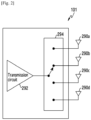
- FIG. 2 is a diagram of an electronic device that performs a TAS operation according to an embodiment of the disclosure.
- the electronic device 101 may include a single transmission circuit 292.
- the transmission circuit 292 is a circuit including at least one of a power amplifier (PA), a low noise amplifier (LNA), a duplexer, a switch, or a filter, and may be referred to as a FEM. If sounding reference signals (SRSs) are transmitted via four antennas 290a, 290b, 290c, and 290d, it may be difficult to simultaneously transmit SRSs via the four antennas 290a, 290b, 290c, and 290d since the number of transmission circuits 292 are limited.
- SRSs sounding reference signals
- the transmission circuit 292 is sequentially connected to the four antennas 290a, 290b, 290c, and 290d using the switch 294. Accordingly, the electronic device 101 may transmit SRSs via the four antennas 290a, 290b, 290c, and 290d.
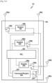
- FIG. 3A is a block diagram the communication module 190 in the electronic device 101 according to an embodiment of the disclosure.
- FIG. 3A illustrates the configuration of the communication module 190 for supporting the TAS operation, and the configuration includes four antennas and a single FEM including a transmission circuit.
- the communication module 190 may include a first antenna 290a, a second antenna 290b, a third antenna 290c, a fourth antenna 290d, a radio frequency integrated circuit (RFIC) 392, a transmission/reception FEM 394, a transmission switch 294, a first reception FEM 396a, a first switch 398a, a second reception FEM 396b, a second switch 398b, a third reception FEM 396c, and/or a third switch 398c.
- RFIC radio frequency integrated circuit
- the first antenna 290a may be connected to the transmission/reception FEM 394 depending on the state of the transmission switch 294.
- the second antenna 290b may be connected to the transmission/reception FEM 394 or the first reception FEM 396a, depending on the states of the transmission switch 294 and the first switch 398a.
- the third antenna 290c may be connected to the transmission/reception FEM 394 or the second reception FEM 396b, depending on the states of the transmission switch 294 and the second switch 398b.
- the fourth antenna 290d may be connected to the transmission/reception FEM 394 or the third reception FEM 396c, depending on the states of the transmission switch 294 and the third switch 398c.
- the RFIC 392 may generate a signal to be transmitted via at least one of the first antenna 290a, the second antenna 290b, the third antenna 290c, and the fourth antenna 290d, or may interpret a signal received via at least one of the first antenna 290a, the second antenna 290b, the third antenna 290c, and the fourth antenna 290d.
- the RFIC 392 may perform at least one of signal modulation/demodulation, frequency modulation, and/or analog/digital conversion.
- the transmission/reception FEM 394 may include a circuit for processing a transmission signal and a reception signal.
- the transmission/reception FEM 394 may perform at least one operation among amplification of a transmission signal, amplification of a reception signal, and/or filtering a transmission signal or reception signal.
- the transmission FEM 394 may be referred to as "transmission/reception path", “low noise amplifier power amplifier module-with duplexer (LPAMiD)", or other terms having a technical meaning equivalent thereto.
- Each of the first reception FEM 396a, the second reception FEM 396b, and the third reception FEM 396c may include a circuit for processing a reception signal.
- each of the first reception FEM 396a, the second reception FEM 396b, and the third reception FEM 396c may perform at least one operation among amplification of a reception signal and/or filtering a reception signal.
- Each of the first reception FEM 396a, the second reception FEM 396b, and the third reception FEM 396c may be referred to as "reception path", “low noise amplifier-FEM (LFEM)", or other terms having a technical meaning equivalent thereto.
- LFEM low noise amplifier-FEM
- the transmission switch 294, the first switch 398a, the second switch 398b, or the third switch 398c may form a signal path among different components.
- the connection state of each of the transmission switch 294, the first switch 398a, the second switch 398b, or the third switch 398c may be changed according to the control of the processor (e.g., a communication processor or the processor 120 of FIG. 1 ).
- At least one of the first switch 398a, the second switch 398b, or the third switch 398c may be controlled to connect at least one of the first reception FEM 398a, the second reception FEM 398b, or the third reception FEM 398c, and the transmission switch 294, and the transmission switch 294 may be controlled to sequentially connect a selected number of antennas and the transmission/reception FEM 394.
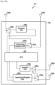
- FIG. 3B is a block diagram of a communication module in an electronic device according to an embodiment of the disclosure.
- FIG. 3B illustrates a configuration of the communication module 190 for supporting a TAS operation, and the configuration includes four antennas and two FEMs including transmission circuits.
- the communication module 190 may include the first antenna 290a, the second antenna 290b, the third antenna 290c, the fourth antenna 290d, the RFIC 392, a first transmission/reception FEM 394a, a first transmission switch 294a, a second transmission/reception FEM 394b, a second transmission switch 294b, the first reception FEM 396a, the first switch 398a, the second reception FEM 396b, and/or the second switch 398b.
- Each of the first antenna 290a and the second antenna 290b may be connected to the first transmission/reception FEM 394a or the first reception FEM 396a, depending on the states of the first transmission switch 294a and the first switch 398a which are controlled by a processor (e.g., a communication processor or the processor 120 of FIG. 1 ).
- a processor e.g., a communication processor or the processor 120 of FIG. 1
- Each of the third antenna 290c and the fourth antenna 290d may be connected to the second transmission/reception FEM 394b or the second reception FEM 396b, depending on the states of the second transmission switch 294b and the second switch 398b which are controlled by a processor (e.g., a communication processor or the processor 120 of FIG. 1 ).
- two transmission/reception FEMs 394a and 394b may be included, unlike FIG. 3A .
- the electronic device 101 may transmit sounding reference signals (SRSs) via two antennas (e.g., the first antenna 290a and the third antenna 290c) in parallel, using the two transmission/reception FEMs 394a and 394b.
- SRSs sounding reference signals
- FIG. 3A illustrates the case in which a single transmission circuit (e.g., the transmission/reception FEM 394) is included.
- FIG. 3B illustrates the case in which two transmission circuits (e.g., the first transmission/reception FEM 394a and the second transmission/reception FEM 394b) are included.
- the first transmission/reception FEM 394a and the second transmission/reception FEM 394b are included.
- an antenna switching operation and/or operations according to various embodiments described below may be performed.
- FIG. 4 is a block diagram of a transmission/reception FEM (e.g., the transmission/reception FEM 394, 394a, or 394b) of the communication module in the electronic device according to an embodiment of the disclosure.
- a transmission/reception FEM e.g., the transmission/reception FEM 394, 394a, or 394b
- the transmission/reception FEM 394, 394a, or 394b may include a power amplifier (PA) 410, a low noise amplifier (LNA) 420, a switch 430, a filter 440, and/or a coupler 450.
- a transmission signal may be amplified by the power amplifier 410, may pass through the switch 430, may be filtered by the filter 440 based on a transmission band, and may be output to an antenna.
- a reception signal provided from an antenna may be filtered by the filter 440 based on a reception band, may pass through the switch 430, and may be amplified by the low noise amplifier 420.
- the low noise amplifier 420 may be omitted.
- an RFIC (e.g., the RFIC 392) that receives a reception signal may include a low noise amplifier.
- the coupler 450 may include a forward terminal 452 and/or a reverse terminal 454.
- the forward terminal 452 may be used to extract a signal delivered from the filter 440 to an antenna.
- the reverse terminal 454 may be used to extract a signal delivered from an antenna to the filter 440.
- FIG. 5 is a block diagram of a reception FEM (e.g., the reception FEM 396a, 396b, or 396c) of a communication module in an electronic device according to an embodiment of the disclosure.
- a reception FEM e.g., the reception FEM 396a, 396b, or 396c
- the reception FEM 396a, 396b, or 396c may include a filter 510, a low noise amplifier 520, and/or a bypass path 530.
- a reception signal provided from an antenna may be filtered by the filter 510, may be amplified by the low noise amplifier 520 or may pass through the bypass path 530, and may be transferred to an RFIC (e.g., the RFIC 392).
- an electronic device e.g., the electronic device 101 of FIG. 1
- a plurality of antennas e.g., the antennas 290a, 290b, 290c, and 290d
- FEM reception front end module
- at least one transmission/reception FEM e.g., transmission/reception FEM 394
- at least one switch e.g., the transmission switch 294, the first switch 398a, the second switch 398b, and the third switch 398c
- the at least one processor is configured to: transmit a signal via a first antenna subset (e.g., the first antenna 290a) including at least one of the plurality of antennas; measure the emission environment of the plurality of antennas, using the signal; determine at least one antenna to be used for transmission of a sounding reference signal (SRS), based on the emission environment; and transmit the SRS via the at least one determined antenna.
- the emission environment includes the strength of a reflected signal that corresponds to the signal and is reflected by the first antenna subset, or the strength of a reception signal that corresponds to the signal and is detected by a second antenna subset (e.g., the second antenna 290b, the third antenna 290c, and the fourth antenna 290d) including at least one remaining antenna.
- the emission environment may be determined based on the ratio of the strength of the reflected signal to the strength of the signal, or the ratio of the strength of the reception signal to the strength of the signal.
- the at least one processor may further be configured to transmit the SRS by sequentially switching the at least one antenna.
- the first antenna subset (e.g., the first antenna 290a) may include as many antennas as the number of the at least one transmission/reception FEMs.
- the at least one processor may further be configured to: measure the strength of a reflected signal corresponding to at least one antenna included in the first antenna subset (e.g., the first antenna 290a); and measure a strength of a reception signal detected by at least one antenna included in the second antenna subset if the strength of the reflected signal is less than a first threshold value.
- the at least one processor may further be configured to transmit, to a base station, capability information related to a transmit antenna switching (TAS) operation that transmits the SRS by sequentially switching the plurality of antennas (e.g., the antennas 290a, 290b, 290c, and 290d).
- TAS transmit antenna switching
- the capability information indicates at least one of whether to perform the TAS operation or a number of antennas switched by the TAS operation.
- the at least one processor may further be configured to change an antenna used for uplink communication with a base station, if the strength of the reflected signal exceeds a threshold value.
- the at least one processor may further be configured to measure the emission environment of the plurality of antennas, in response to start of a service that requires a data transmission rate greater than or equal to a threshold value, or in response to a data error rate, less than or equal to a threshold value, during multiple input multiple output (MIMO) reception.
- MIMO multiple input multiple output
- the electronic device 101 may perform a TAS operation using the above-mentioned configuration.
- the electronic device 101 may measure an emission environment, and may control whether to perform the TAS operation and/or a configuration associated with the TAS operation, based on the emission environment.
- the emission environment may be related to a quality of a channel that a plurality of antennas, which may be switched by the TAS operation, may experience, and may be related to whether a gain occurs by MIMO technology.
- the emission environment may be related to a factor that occurs during a relatively long period of time, such as a condition of holding or a weak electric field, as opposed to a short time fading which occurs randomly.
- FIG. 6 is a flowchart 600 illustrating a process of transmitting a sounding reference signal (SRS) by an electronic device according to an embodiment of the disclosure.
- the subject that performs the operations in the flowchart 600 of FIG. 6 is understood as the electronic device 101 or the components (e.g., the processor 120 or the communication module 190) of the electronic device 101.
- the electronic device 101 transmits a signal via a first antenna subset.
- the signal is transmitted via an uplink resource allocated by a base station for uplink communication.
- the signal includes data (e.g., traffic or control information) for communication with the base station.
- the first antenna subset includes at least one antenna allocated for uplink communication, for example, the first antenna 290a of FIG. 3A .
- an uplink signal generated by the RFIC 392 is processed by the transmission/reception FEM 394, and is transmitted via the first antenna 290a.
- the electronic device 101 measures the emission environment of the first antenna subset and a second antenna subset using the transmitted signal.
- the second antenna subset includes at least one antenna, remaining after excluding at least one antenna included in the first antenna subset, among the usable antennas.
- the electronic device 101 measures the emission environment of the first antenna subset and the second antenna subset, without generating an additional signal.
- the emission environment is measured in order to estimate the level of gain which is obtained when MIMO reception is performed using the first antenna subset and the second antenna subset. For example, if an antenna is blocked due to holding by a user, the emission environment is measured to be poor when the electronic device 101 enters a weak electric field.
- the electronic device 101 determines the transmission scheme of a sounding reference signal (SRS), based on the emission environment.
- the transmission scheme of an SRS includes the number of antennas to be used for transmitting an SRS and/or whether to transmit an SRS.
- the number of antennas to be used for transmitting an SRS depends on the number of antennas that are present in an emission environment above a predetermined level.
- the electronic device 101 operates according to the determined transmission scheme of an SRS. If it is determined that a plurality of antennas are to be used for transmitting an SRS, the electronic device 101 transmits SRSs via a plurality of antennas using a TAS operation. If it is determined that a single antenna is to be used for transmitting an SRS, the electronic device transmits an SRS without performing a TAS operation.
- FIG. 7A is a flowchart 700 illustrating a process of measuring an emission environment using a reception signal, by an electronic device according to an embodiment of the disclosure.
- the subject that performs the operations in the flowchart 700 of FIG. 7A may be understood as the electronic device 101 or the components (e.g., the processor 120 or the communication module 190) of the electronic device 101.
- FIG. 7A illustrates operations for measuring an emission environment for at least one antenna included in a second antenna subset.
- a first antenna is included in a first antenna subset
- a second antenna is included in the second antenna subset.
- the electronic device 101 may receive, using the second antenna, a signal transmitted via the first antenna.
- the electronic device 101 may transmit a signal via the first antenna.
- the signal transmitted via the first antenna may be received via the second antenna included in the electronic device 101.
- the electronic device 101 may measure the strength of the signal received by the second antenna.
- the electronic device 101 may process the signal received by the second antenna, and may measure the strength of the signal, using a reception circuit (e.g., the reception FEM 396a) which is not used for communication with the base station during uplink communication.
- the strength of the signal received by the second antenna may be used as an index indicating a channel state associated with the second antenna (e.g., the state of being blocked by an obstacle or the state of being in a weak electric field).
- the fact that the signal that is transmitted via the first antenna and is received by the second antenna has a high strength may mean that a signal that is to be transmitted from the base station and is to be received by the second antenna may also have a high strength.
- FIG. 7B is a diagram illustrating circuits used when an electronic device measures an emission environment using a reception signal according to an embodiment of the disclosure.
- the transmission switch 294 may form a path between the transmission/reception FEM 394 and the first antenna 290a, and the first switch 398a may form a path between the reception FEM 396a and the second antenna 290b.
- a signal that is transmitted via the first antenna 290a after passing through the transmission/reception FEM 394 may be received by the second antenna 290b, and the received signal may be provided to the reception FEM 396a.
- the received signal may pass through a bypass path 530 of the reception FEM 396a, and may be provided to the RFIC 392.
- the RFIC 392 may measure the strength of the signal, and may determine a value indicating the emission environment of the second antenna 290b.
- the signal may pass through the bypass path 530, and may be provided to the RFIC 392.
- a low transmission power e.g., 0 dBm
- a signal with a power greater than a reception power of about -35 dBm may be detected. Since the power of the detected signal is greater than the power of the reception signal from the base station, it is determined that the measured value is reliable although the signal passes through the bypass path 530 of the reception FEM 396a.
- the signal may pass through a low noise amplifier (e.g., the low noise amplifier 520) and may be provided to the RFIC 392.
- a received signal is configured to always pass through a low noise amplifier, or is configured to selectively pass through a low noise amplifier according to the size of a signal.
- the value indicating the emission environment of the second antenna may be determined based on the strength of a received signal.
- the strength of a received signal may depend on the strength of a transmitted signal.
- the performance or efficiency of an antenna does not change depending on the strength of a transmitted signal.
- the ratio of the strength of a transmitted signal to the strength of a received signal may be expected to be constant if the external environment does not change.
- the ratio of the strength of a transmitted signal to the strength of a received signal may be constant if the external environment does not change.
- the value indicating the emission environment of the second antenna 290b may be determined based on a result of comparison between the strength of a signal transmitted via the first antenna (e.g., the first antenna 290a) and the strength of a signal received via the second antenna 290b.
- the strength of a transmitted signal may be determined based on the strength of a forward signal extracted by a coupler (e.g., the coupler 450) in a transmission/reception FEM, or based on the strength of a signal generated from an RFIC (e.g., the RFIC 392).
- FIG. 8A is a flowchart illustrating a process of measuring an emission environment using a reflected signal, by an electronic device according to an embodiment of the disclosure.
- the subject that performs the operations in the flowchart of FIG. 8 may be understood as the electronic device 101 or the components (e.g., the processor 120 or the communication module 190) of the electronic device 101.
- FIG. 8A illustrates operations of measuring an emission environment for at least one antenna included in a first antenna subset.
- a first antenna may be included in the first antenna subset.
- the electronic device 101 may detect a reflected signal that corresponds to a signal transmitted via the first antenna.
- the electronic device 101 may transmit a signal via the first antenna. If a signal is output from a transmission circuit to an antenna for uplink communication, a part of the signal may not be emitted via the antenna but may be reflected. In order to detect the reflected signal, the electronic device 101 may perform coupling of the reflected signal in the transmission circuit.
- the electronic device 101 may measure the strength of the reflected signal.
- the strength of the reflected signal from the first antenna may be used as an index indicating a channel state associated with the first antenna (e.g., the state of being blocked by an obstacle or the state of being in a weak electric field).
- the fact that a reflected signal from the first antenna is detected and the detected reflected signal has a high strength may mean that the first antenna is in a poor emission environment.
- FIG. 8B is a diagram illustrating circuits used when an electronic device measures an emission environment using a reflected signal according to an embodiment of the disclosure.
- the transmission switch 294 may form a path between the transmission/reception FEM 394 and the first antenna 290a.
- the coupler 450 in the transmission/reception FEM 394 may extract a reflected signal using a terminal (e.g., the reverse terminal 454) for extracting a reverse signal.
- the extracted signal may be provided to the RFIC 392.
- the RFIC 392 may measure the strength of the reflected signal, and may determine a value indicating the emission environment of the first antenna 290a. For example, the RFIC 392 may digitalize the reflected signal using an analog to digital converter (ADC), and may measure the strength of the signal.
- ADC analog to digital converter
- the value indicating the emission environment for the first antenna may be determined based on the strength of a reflected signal.
- the strength of a reflected signal may depend on the strength of a transmitted signal.
- the ratio of the strength of a transmitted signal to the strength of a reflected signal may be expected to be constant if the external environment does not change.
- the ratio of the strength of a transmitted signal to the strength of a reflected signal may be constant if the external environment does not change.
- the value indicating the emission environment of the first antenna 290a may be determined based on a result of comparison between the strength of a signal transmitted via the first antenna (e.g., the first antenna 290a) and the strength of a signal received via the first antenna 290a.
- the strength of a transmitted signal may be determined based on the strength of a forward signal extracted by a coupler (e.g., 450) in a transmission/reception FEM, or based on the strength of a signal generated from an RFIC (e.g., the RFIC 392).
- the operations described with reference to FIGS. 7A and 7B may be repeated as many times as the number of antennas included in the second antenna subset, and the operations described with reference to FIGS. 8A and 8B may be repeated as many times as the number of antennas included in the first antenna subset. For example, if the first antenna subset includes a single antenna and the second antenna subset includes three antennas, the travel path of a signal according to the measurement of the emission environment may be as shown in FIG. 9 .
- FIG. 9 is a diagram illustrating a travel path of a signal used when the electronic device 101 measures an emission environment according to an embodiment of the disclosure.
- the transmission signal may arrive at the second antenna 290b via a first path 901, may arrive at the third antenna 290c via a second path 902, or may arrive at the fourth antenna 290d via a third path 903.
- a part of the transmission signal may be reflected by the first antenna 290a, and the reflected signal may flow in a circuit via a fourth path 904.
- the electronic device 101 may measure an emission environment for the antennas 290a, 290b, 290c, and 290d.
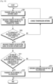
- FIG. 10 is a flowchart 1000 illustrating a process of transmitting a sounding reference signal (SRS), by an electronic device according to an embodiment of the disclosure.
- the subject that performs the operations in the flowchart 1000 of FIG. 10 may be understood as the electronic device 101 or the components (e.g., the processor 120 or the communication module 190) of the electronic device 101.
- the electronic device 101 may transmit a signal via a first antenna subset.
- the first antenna subset may include at least one antenna connected to a transmission circuit (e.g., the transmission/reception FEM 394).
- the electronic device 101 may transmit a signal including uplink data (e.g., traffic or control information) for communication with a base station.
- the electronic device 101 may measure the strength of a reflected signal corresponding to the transmitted signal.
- the electronic device 101 may detect the reflected signal, which is not transmitted via the first antenna subset but is reflected, and may measure the strength of the reflected signal.
- the electronic device 101 may identify whether the strength of the reflected signal is less than a threshold value.
- the threshold value may be defined.
- the electronic device 101 may evaluate the emission environment of at least one antenna included in the first antenna subset, for example, the emission environment of a transmission antenna, based on the strength of the reflected signal.
- the electronic device 101 may change the transmission antenna in operation 1007.
- the fact that the strength of the reflected signal is greater than or equal to the threshold value means that the emission environment is poor. Accordingly, the electronic device 101 may change an antenna used for transmission to another antenna.
- the electronic device 101 may measure the strength of a reception signal in a second antenna subset in operation 1009.
- a reception circuit is not used for uplink communication, and thus, the electronic device 101 may process a signal, which is transmitted via the first antenna subset and is received via least one antenna included in the second antenna subset, using the reception circuit.
- the electronic device 101 may identify whether one or more antennas, at which the strength of a reception signal is greater than or equal to a threshold value, exist.
- the electronic device 101 may identify the number of antennas that detect a signal of which the strength is greater than or equal to the threshold value, among at least one antenna included in the second antenna subset.
- the electronic device 101 may perform communication without a TAS operation in operation 1013. For example, the electronic device 101 may transmit a sounding signal using at least one antenna included in the first antenna subset, or may operate without transmission of a sounding signal. According to an embodiment of the disclosure, if a plurality of antennas are included in the first antenna subset, for example, if a plurality of transmission circuits are included, the electronic device 101 may transmit SRSs via the plurality of antennas included in the first antenna subset using a TAS operation.
- the electronic device 101 may transmit an SRS using a TAS operation in operation 1015. At least one antenna included in the first antenna subset and at least one antenna included in the second antenna subset are usable for transmission of an SRS, and thus, the electronic device 101 may use at least two antennas. The electronic device 101 may transmit SRSs via at least two antennas using a TAS operation.
- the electronic device 101 may determine the number of antennas used for transmitting an SRS, based on the emission environment of antennas. According to an embodiment of the disclosure, if the number of antennas is determined, the electronic device 101 may transmit TAS operation-related information to a base station.
- the TAS operation-related information is capability information of the electronic device 101, and may indicate at least one of whether to perform a TAS operation, the number of antennas switched by a TAS operation, and/or the number of streams supportable for MIMO reception.
- the electronic device 101 may transmit capability information indicating that a TAS operation using two antennas is allowed or a two-receive (RX) MIMO operation is allowed.
- RX two-receive
- the electronic device 101 may transmit capability information indicating that a TAS operation using four antennas is allowed and capability information indicating that a four-RX MIMO operation is allowed.
- the TAS operation-related information which is transmitted to a base station, may be utilized for scheduling by the base station.
- the base station may determine the amount of resources (e.g., the number of symbols) used for transmission of an SRS, based on the TAS operation-related information, and may determine the number of streams to be transmitted via MIMO transmission. For example, based on the number of antennas to be switched by a TAS operation, the base station may allocate a resource for transmitting an SRS for the electronic device 101. For example, if the TAS operation is not performed, the base station may not perform MIMO transmission for the electronic device 101, and may not allocate a resource for transmitting an SRS.
- FIG. 11 is diagram illustrating examples of resource usage by an electronic device according to an embodiment of the disclosure.
- sounding reference signals may be transmitted in a plurality of symbols or slots.
- the electronic device 101 may be scheduled to transmit SRSs according to a first situation 1110.
- the electronic device 101 may be scheduled to perform downlink communication or uplink communication without transmission of SRSs.
- the electronic device 101 may transmit capability information, indicating not performing of a TAS operation, to a base station, before the interval 1122. Accordingly, the base station may not allocate a resource for transmitting an SRS in the interval 1122.
- the electronic device 101 may measure an emission environment, and may determine whether to perform a TAS operation according to the measured emission environment. According to an embodiment of the disclosure, if a predetermined condition is satisfied, the electronic device 101 may measure an emission environment in order to determine whether to perform a TAS operation. For example, an emission environment may be measured if a change in the emission environment is expected, or if MIMO reception is needed. For example, in response to start of a service that requires a data transmission rate greater than or equal to a threshold value, a data error rate less than or equal to a threshold value during MIMO reception, and a rapid increase in a data error rate during MIMO reception, the electronic device 101 may perform operations of measuring an emission environment.
- a method of an electronic device may include: transmitting a signal via a first antenna subset (e.g., the first antenna 290a) including at least one of a plurality of antennas (e.g., antennas 290a, 290b, 290c, and 290d); measuring an emission environment of the plurality of antennas, using the signal; determining at least one antenna to be used for transmitting a sounding reference signal (SRS), based on the emission environment; and transmitting the SRS via the at least one determined antenna.
- a first antenna subset e.g., the first antenna 290a
- a plurality of antennas e.g., antennas 290a, 290b, 290c, and 290d
- SRS sounding reference signal
- the emission environment may include the strength of a reflected signal that corresponds to the signal and is reflected by the first antenna subset, or the strength of a reception signal that corresponds to the signal and is detected by a second antenna subset (e.g., the second antenna 290b, the third antenna 290c, and the fourth antenna 290d) including at least one remaining antenna.
- a second antenna subset e.g., the second antenna 290b, the third antenna 290c, and the fourth antenna 290d
- the emission environment may be determined based on the ratio of the strength of the reflected signal to the strength of the signal, or the ratio of the strength of the reception signal to the strength of the signal.
- the operation of transmitting the reference signal may include: transmitting the SRS by sequentially switching the at least one antenna.
- the first antenna subset (e.g., the first antenna 290a) may include as many antennas as the number of front end modules (FEMs) (e.g., the transmission/reception FEM 394) for transmission.
- FEMs front end modules
- the signal transmitted via the first antenna subset may be transmitted via a resource allocated for uplink communication with a base station.
- the operation of measuring the emission environment of the plurality of antennas (e.g., the antennas 290a, 290b, 290c, and 290d) using the signal may include: measuring the strength of a reflected signal corresponding to at least one antenna included in the first antenna subset (e.g., the first antenna 290a); and if the strength of the reflected signal is less than a first threshold value, measuring a strength of a reception signal detected by at least one antenna included in the second antenna subset.
- the method may further include: transmitting, to a base station, capability information related to a transmit antenna switching (TAS) operation which transmits the SRS by sequentially switching the plurality of antennas (e.g., the antennas 290a, 290b, 290c, and 290d).
- TAS transmit antenna switching
- the capability information may indicate at least one of whether to perform the TAS operation, or a number of antennas to be switched by the TAS operation.
- the method may further include: changing an antenna used for uplink communication with a base station if the strength of the reflected signal exceeds a threshold value.
- the operation of measuring the emission environment of the plurality of antennas may include: measuring the emission environment of the plurality of antennas in response to start of a service that requires a data transmission rate greater than or equal to a threshold value, or in response to a data error rate, less than or equal to a threshold value, during MIMO reception.
- the electronic device 101 may recognize the emission environment of antennas, without using an additional resource or power. From the perspective of the electronic device 101, the electronic device 101 may determine with high reliability an emission environment for each antenna by using a transmission signal, which has a high strength when being received.
- resources available for data communication may be more secured by reducing unnecessary SRS transmission, and thus, throughput may be improved. Also, unnecessary power consumption by the electronic device 101 may be prevented and a battery duration time may be increased, by reducing unnecessary SRS transmission.
- An electronic device may be one of the various types of devices.
- the electronic device may include, for example, a portable communication device (e.g., a smart phone), a computer device, a portable multimedia device, a portable medical device, a camera, a wearable device, or home appliances.
- a portable communication device e.g., a smart phone
- the electronic device according to an embodiment is not limited to the above-described devices.
- the electronic device may be one of various types of electronic devices.
- the electronic devices may include, for example, a portable communication device (e.g., a smartphone), a computer device, a portable multimedia device, a portable medical device, a camera, a wearable device, or a home appliance. According to an embodiment of the disclosure, the electronic devices are not limited to those described above.
- module may include a unit implemented in hardware, software, or firmware, and may interchangeably be used with other terms, for example, “logic,” “logic block,” “part,” or “circuitry”.
- a module may be a single integral component, or a minimum unit or part thereof, adapted to perform one or more functions.
- the module may be implemented in a form of an application-specific integrated circuit (ASIC).
- ASIC application-specific integrated circuit
- Various embodiments as set forth herein may be implemented as software (e.g., the program 140) including one or more instructions that are stored in a storage medium (e.g., internal memory 136 or external memory 138) that is readable by a machine (e.g., the electronic device 101).
- a processor e.g., the processor 120
- the machine e.g., the electronic device 101
- the one or more instructions may include a code generated by a complier or a code executable by an interpreter.
- the machine-readable storage medium may be provided in the form of a non-transitory storage medium.
- non-transitory simply means that the storage medium is a tangible device, and does not include a signal (e.g., an electromagnetic wave), but this term does not differentiate between where data is semi-permanently stored in the storage medium and where the data is temporarily stored in the storage medium.
- a method according to various embodiments of the disclosure may be included and provided in a computer program product.
- the computer program product may be traded as a product between a seller and a buyer.
- the computer program product may be distributed in the form of a machine-readable storage medium (e.g., compact disc read only memory (CD-ROM)), or be distributed (e.g., downloaded or uploaded) online via an application store (e.g., PlayStore TM ), or between two user devices (e.g., smart phones) directly. If distributed online, at least part of the computer program product may be temporarily generated or at least temporarily stored in the machine-readable storage medium, such as memory of the manufacturer's server, a server of the application store, or a relay server.
- CD-ROM compact disc read only memory
- an application store e.g., PlayStore TM
- two user devices e.g., smart phones
- each component e.g., a module or a program of the above-described components may include a single entity or multiple entities. According to various embodiments of the disclosure, one or more of the above-described components may be omitted, or one or more other components may be added. Alternatively or additionally, a plurality of components (e.g., modules or programs) may be integrated into a single component. In such a case, according to various embodiments of the disclosure, the integrated component may still perform one or more functions of each of the plurality of components in the same or similar manner as they are performed by a corresponding one of the plurality of components before the integration.
- operations performed by the module, the program, or another component may be carried out sequentially, in parallel, repeatedly, or heuristically, or one or more of the operations may be executed in a different order or omitted, or one or more other operations may be added.
Landscapes
- Engineering & Computer Science (AREA)
- Signal Processing (AREA)
- Computer Networks & Wireless Communication (AREA)
- Quality & Reliability (AREA)
- Physics & Mathematics (AREA)
- Electromagnetism (AREA)
- Mobile Radio Communication Systems (AREA)
- Transceivers (AREA)
Claims (13)
- Procédé de fonctionnement d'un dispositif électronique (101), le procédé comprenant :transmettre (601) un signal par l'intermédiaire d'un premier sous-ensemble d'antennes comprenant au moins une antenne parmi une pluralité d'antennes (290a à 290d) ;mesurer (603) un environnement d'émission de la pluralité d'antennes (290a à 290d), en utilisant le signal ;déterminer (605) au moins une antenne à utiliser pour transmettre un signal de référence de sondage, SRS, en fonction de l'environnement d'émission ; ettransmettre (607) le SRS par l'intermédiaire de l'au moins une antenne déterminée,dans lequel l'environnement d'émission est déterminé en fonction d'une intensité d'un signal réfléchi correspondant au signal et réfléchi par le premier sous-ensemble d'antennes, ou d'une intensité d'un signal de réception correspondant au signal et reçu par un deuxième sous-ensemble d'antennes comprenant au moins une antenne restante,le procédé étant caractérisé en ce quela mesure de l'environnement d'émission de la pluralité d'antennes (290a à 290d) à l'aide du signal comprend :mesurer l'intensité du signal réfléchi correspondant à au moins une antenne incluse dans le premier sous-ensemble d'antennes ; etsi l'intensité du signal réfléchi est inférieure à une première valeur seuil, mesurer l'intensité du signal de réception détecté par au moins une antenne incluse dans le deuxième sous-ensemble d'antennes.
- Procédé de la revendication 1, dans lequel l'environnement d'émission est déterminé sur la base d'un rapport entre l'intensité du signal réfléchi et l'intensité du signal, ou d'un rapport entre l'intensité du signal de réception et l'intensité du signal.
- Procédé de la revendication 1, dans lequel la transmission du SRS comprend :
transmettre le SRS en commutant séquentiellement l'au moins une antenne à utiliser pour la transmission du SRS. - Procédé de la revendication 1, dans lequel le premier sous-ensemble d'antennes comprend autant d'antennes qu'un nombre de modules frontaux, FEM, pour la transmission.
- Procédé de la revendication 1, dans lequel le signal transmis via le premier sous-ensemble d'antennes est transmis via une ressource allouée pour la communication en liaison montante avec une station de base.
- Procédé de la revendication 1, comprenant en outre :
transmettre, à une station de base, des informations de capacité relatives à une opération de commutation d'antenne de transmission, TAS, qui transmet le SRS en commutant séquentiellement la pluralité d'antennes. - Procédé de la revendication 1, comprenant en outre :
changer une antenne utilisée pour la communication en liaison montante avec une station de base si l'intensité du signal réfléchi dépasse une valeur seuil. - Dispositif électronique (101), comprenant :une pluralité d'antennes (290a à 290d) ;au moins un module frontal de réception, FEM (396c, 396b, 396a), configuré pour traiter un signal de réception reçu via au moins l'une de la pluralité d'antennes (290a à 290d) ;au moins un FEM de transmission/réception (394) configurée pour traiter un signal de transmission transmis via au moins une des antennes (290a à 290d) et un signal de réception reçu via au moins une de la pluralité d'antennes (290a à 290d) ;au moins un commutateur (294) configuré pour former un chemin entre l'au moins un FEM de réception, l'au moins un FEM de transmission et la pluralité d'antennes (290a à 290d) ; etun processeur (120),dans lequel le processeur (120) est configuré pour :transmettre un signal via un premier sous-ensemble d'antennes comprenant au moins une de la pluralité d'antennes (290a à 290d) ;mesurer un environnement d'émission de la pluralité d'antennes (290a à 290d), en utilisant le signal ;déterminer au moins une antenne à utiliser pour la transmission d'un signal de référence de sondage, SRS, en fonction de l'environnement d'émission ; ettransmettre le SRS par l'intermédiaire de l'au moins une antenne déterminée,dans lequel l'environnement d'émission comprend une intensité d'un signal réfléchi qui correspond au signal et est réfléchi par le premier sous-ensemble d'antennes, ou une intensité d'un signal de réception qui correspond au signal et est reçu par un deuxième sous-ensemble d'antennes comprenant au moins une antenne restante,le dispositif électronique (101) étant caractérisé en ce que le processeur (120) est configuré pour :mesurer l'intensité du signal réfléchi correspondant à au moins une antenne incluse dans le premier sous-ensemble d'antennes ; etsi l'intensité du signal réfléchi est inférieure à une première valeur seuil, mesurer l'intensité du signal de réception détecté par au moins une antenne incluse dans le deuxième sous-ensemble d'antennes.
- Dispositif électronique (101) de la revendication 8, dans lequel l'environnement d'émission est déterminé sur la base d'un rapport entre l'intensité du signal réfléchi et une intensité du signal, ou d'un rapport entre l'intensité du signal de réception et l'intensité du signal.
- Dispositif électronique (101) de la revendication 8, dans lequel le processeur (120) est configuré pour transmettre le SRS en commutant séquentiellement l'au moins une antenne à utiliser pour la transmission pour le SRS.
- Dispositif électronique (101) de la revendication 8, dans lequel le premier sous-ensemble d'antennes comprend autant d'antennes qu'un nombre de l'au moins un FEM de transmission/réception.
- Dispositif électronique (101) de la revendication 8, dans lequel le signal transmis via le premier sous-ensemble d'antennes est transmis via une ressource allouée pour la communication en liaison montante avec une station de base.
- Dispositif électronique (101) de la revendication 8, dans lequel le processeur (120) est configuré pour transmettre, à une station de base, des informations de capacité relatives à une opération de commutation d'antenne de transmission, TAS, qui transmet le SRS en commutant séquentiellement la pluralité d'antennes.
Applications Claiming Priority (2)
| Application Number | Priority Date | Filing Date | Title |
|---|---|---|---|
| KR1020190038991A KR102697373B1 (ko) | 2019-04-03 | 2019-04-03 | 사운딩 기준 신호를 송신하기 위한 방법 및 그 전자 장치 |
| PCT/KR2020/004579 WO2020204658A1 (fr) | 2019-04-03 | 2020-04-03 | Procédé d'émission de signal de référence de sondage et dispositif électronique pour cela |
Publications (3)
| Publication Number | Publication Date |
|---|---|
| EP3912301A1 EP3912301A1 (fr) | 2021-11-24 |
| EP3912301A4 EP3912301A4 (fr) | 2022-03-23 |
| EP3912301B1 true EP3912301B1 (fr) | 2023-12-27 |
Family
ID=72662472
Family Applications (1)
| Application Number | Title | Priority Date | Filing Date |
|---|---|---|---|
| EP20781787.5A Active EP3912301B1 (fr) | 2019-04-03 | 2020-04-03 | Procédé d'émission de signal de référence de sondage et dispositif électronique pour cela |
Country Status (4)
| Country | Link |
|---|---|
| US (2) | US11206066B2 (fr) |
| EP (1) | EP3912301B1 (fr) |
| KR (1) | KR102697373B1 (fr) |
| WO (1) | WO2020204658A1 (fr) |
Families Citing this family (10)
| Publication number | Priority date | Publication date | Assignee | Title |
|---|---|---|---|---|
| CN114640370B (zh) * | 2020-12-16 | 2023-04-11 | Oppo广东移动通信有限公司 | 射频收发系统及通信设备 |
| CN112583504B (zh) * | 2020-12-16 | 2022-09-06 | 维沃移动通信有限公司 | 天线切换方法及装置 |
| CN114640371B (zh) * | 2020-12-16 | 2023-05-05 | Oppo广东移动通信有限公司 | 射频收发系统及通信设备 |
| CN114640369B (zh) * | 2020-12-16 | 2023-03-24 | Oppo广东移动通信有限公司 | 射频收发系统及通信设备 |
| US12041001B2 (en) * | 2021-01-27 | 2024-07-16 | Skyworks Solutions, Inc. | Unified sounding reference signal input/output functionality |
| KR102909708B1 (ko) * | 2021-01-28 | 2026-01-09 | 삼성전자주식회사 | 전자 장치, 전자 장치의 동작 방법 및 폴더블 전자 장치 |
| CN113258944B (zh) * | 2021-05-12 | 2023-05-16 | 展讯通信(上海)有限公司 | Srs发射电路、方法和装置 |
| CN113938224B (zh) * | 2021-09-18 | 2024-03-15 | 青岛海信移动通信技术有限公司 | 一种信息传输方法、终端及装置 |
| CN115133950B (zh) * | 2022-06-29 | 2024-03-26 | 联想(北京)有限公司 | 一种信号收发电路、测量方法及装置 |
| WO2025121816A1 (fr) * | 2023-12-08 | 2025-06-12 | 삼성전자 주식회사 | Dispositif électronique pour prendre en charge une transmission de signal de référence et son procédé de commande |
Family Cites Families (15)
| Publication number | Priority date | Publication date | Assignee | Title |
|---|---|---|---|---|
| JPH10107744A (ja) | 1996-09-25 | 1998-04-24 | Matsushita Electric Works Ltd | 無線通信装置の自己診断方法及び装置 |
| JP3973958B2 (ja) | 2002-04-18 | 2007-09-12 | シャープ株式会社 | アンテナ・セルフチェック機能付き受信機 |
| KR20050107916A (ko) | 2004-05-10 | 2005-11-16 | 주식회사 팬택앤큐리텔 | 반사신호를 이용한 안테나 튜닝장치 |
| US8842554B2 (en) * | 2008-05-07 | 2014-09-23 | Mitsubishi Electric Research Laboratories, Inc. | Antenna selection with frequency-hopped sounding reference signals |
| US9287957B2 (en) * | 2009-04-30 | 2016-03-15 | Google Technology Holdings LLC | Method for multi-antenna uplink transmission |
| US9083074B2 (en) | 2012-04-09 | 2015-07-14 | Blackberry Limited | Dynamic antenna selection based on user hand position |
| US9596065B2 (en) * | 2012-10-24 | 2017-03-14 | Qualcomm Incorporated | Enhanced SRS transmission for MIMO operation in LTE-A |
| KR20160039437A (ko) * | 2014-10-01 | 2016-04-11 | 삼성전자주식회사 | 트랜시버 및 그 트랜시버의 동작 방법 |
| CN106549695A (zh) | 2015-09-21 | 2017-03-29 | 北京信威通信技术股份有限公司 | 探测参考信号的发送方法及装置 |
| WO2017081522A1 (fr) * | 2015-11-13 | 2017-05-18 | Telefonaktiebolaget Lm Ericsson (Publ) | Mesure simultanée de vswr et étalonnage de coupleurs sur des ports d'antennes multiples |
| DE102015121967A1 (de) | 2015-12-16 | 2017-06-22 | Intel IP Corporation | Kommunikationsendgerät und Verfahren zum Auswählen einer Übertragungsantenne |
| WO2017192889A1 (fr) * | 2016-05-04 | 2017-11-09 | Intel Corporation | Commutation de panneau d'antenne et indication de faisceau |
| US11558161B2 (en) | 2017-07-27 | 2023-01-17 | Lg Electronics Inc. | Method for transmitting SRS and terminal therefor |
| WO2019043436A1 (fr) | 2017-08-31 | 2019-03-07 | Telefonaktiebolaget Lm Ericsson (Publ) | Systèmes et procédés destinés à une sélection d'antenne de transmission de srs adaptative |
| CN108390694B (zh) * | 2018-03-16 | 2020-05-05 | Oppo广东移动通信有限公司 | 多路选择开关、射频系统以及无线通信设备 |
-
2019
- 2019-04-03 KR KR1020190038991A patent/KR102697373B1/ko active Active
-
2020
- 2020-04-03 US US16/839,529 patent/US11206066B2/en active Active
- 2020-04-03 EP EP20781787.5A patent/EP3912301B1/fr active Active
- 2020-04-03 WO PCT/KR2020/004579 patent/WO2020204658A1/fr not_active Ceased
-
2021
- 2021-12-20 US US17/556,143 patent/US11595091B2/en active Active
Non-Patent Citations (1)
| Title |
|---|
| VIVO: "Discussion on Codebook Based UL Transmission", vol. RAN WG1, no. Prague, CZ; 20171009 - 20171013, 8 October 2017 (2017-10-08), XP051340655, Retrieved from the Internet <URL:http://www.3gpp.org/ftp/Meetings_3GPP_SYNC/RAN1/Docs/> [retrieved on 20171008] * |
Also Published As
| Publication number | Publication date |
|---|---|
| WO2020204658A1 (fr) | 2020-10-08 |
| US11206066B2 (en) | 2021-12-21 |
| EP3912301A1 (fr) | 2021-11-24 |
| US20220116085A1 (en) | 2022-04-14 |
| US11595091B2 (en) | 2023-02-28 |
| KR20200117203A (ko) | 2020-10-14 |
| US20200322015A1 (en) | 2020-10-08 |
| KR102697373B1 (ko) | 2024-08-22 |
| EP3912301A4 (fr) | 2022-03-23 |
Similar Documents
| Publication | Publication Date | Title |
|---|---|---|
| US11595091B2 (en) | Method of transmitting sounding reference signal and electronic device therefor | |
| US11056827B2 (en) | Electronic device and method for identifying state of connection between connector and electrical path | |
| CN112913150A (zh) | 发送上行链路参考信号的电子装置及方法 | |
| CN114008931B (zh) | 用于执行预编码的电子装置及其操作方法 | |
| EP3764552B1 (fr) | Dispositif, et procédé pour commander une transmission d'un dispositif électronique | |
| US20210165441A1 (en) | Electronic device for controlling clock frequency and operating method therefor | |
| EP4329341A1 (fr) | Dispositif et procédé permettant d'établir une connexion | |
| US11546014B2 (en) | Electronic device and method for supporting heterogeneous communication techniques sharing frequency band | |
| EP3806363B1 (fr) | Dispositif électronique de commande de mode de conversion de tension basé sur l'ordre de modulation, et son procédé de fonctionnement | |
| US12562867B2 (en) | Electronic device and method for transmitting reference signal in electronic device | |
| EP4318252A1 (fr) | Dispositif électronique permettant de communiquer avec un dispositif externe par le biais d'une interface usb et son procédé de fonctionnement | |
| US20250330289A1 (en) | Electronic device comprising antenna and method thereof | |
| EP4132087B1 (fr) | Dispositif électronique pour modifier la fréquence de communication sur la base d'une interférence cachée et son procédé de fonctionnement | |
| US12224823B2 (en) | Electronic device and method for transmitting reference signal in electronic device | |
| EP4266823A1 (fr) | Dispositif électronique permettant d'établir une connexion de communication à un dispositif électronique externe et son procédé de fonctionnement | |
| EP4351021A1 (fr) | Dispositif électronique pour identifier l'état d'un circuit associé à une communication | |
| US12074634B2 (en) | Electronic device for cell coverage enhancement and operation method thereof | |
| EP4401492A1 (fr) | Dispositif électronique demandant une attribution de ressources de liaison montante, réseau d'attribution de ressources de liaison montante et procédé de fonctionnement du réseau | |
| US12381592B2 (en) | Wireless communication device including radio frequency integrated circuit and method of controlling the same | |
| US11909435B2 (en) | Method for multi-band communication and electronic device thereof | |
| US12512938B2 (en) | Transmitting sound reference signals (SRSs) based on physical downlink shared channel (PDSCH) scheduling rate | |
| US20250240065A1 (en) | Electronic device for transmitting reference signal and operation method thereof | |
| EP4543054A1 (fr) | Dispositif électronique pour faire fonctionner un groupe principal et un groupe auxiliaire, et procédé de fonctionnement de dispositif électronique | |
| EP4601272A1 (fr) | Dispositif électronique de gestion de protocole entre un circuit de communication et un processeur, procédé de fonctionnement de dispositif électronique | |
| EP4297509A1 (fr) | Dispositif électronique d'attribution de ressource dans un système lan sans fil, et son procédé de fonctionnement |
Legal Events
| Date | Code | Title | Description |
|---|---|---|---|
| STAA | Information on the status of an ep patent application or granted ep patent |
Free format text: STATUS: THE INTERNATIONAL PUBLICATION HAS BEEN MADE |
|
| PUAI | Public reference made under article 153(3) epc to a published international application that has entered the european phase |
Free format text: ORIGINAL CODE: 0009012 |
|
| STAA | Information on the status of an ep patent application or granted ep patent |
Free format text: STATUS: REQUEST FOR EXAMINATION WAS MADE |
|
| 17P | Request for examination filed |
Effective date: 20210816 |
|
| AK | Designated contracting states |
Kind code of ref document: A1 Designated state(s): AL AT BE BG CH CY CZ DE DK EE ES FI FR GB GR HR HU IE IS IT LI LT LU LV MC MK MT NL NO PL PT RO RS SE SI SK SM TR |
|
| A4 | Supplementary search report drawn up and despatched |
Effective date: 20220218 |
|
| RIC1 | Information provided on ipc code assigned before grant |
Ipc: H04B 17/10 20150101ALI20220215BHEP Ipc: H04B 7/06 20060101ALI20220215BHEP Ipc: H04L 5/00 20060101AFI20220215BHEP |
|
| DAV | Request for validation of the european patent (deleted) | ||
| DAX | Request for extension of the european patent (deleted) | ||
| STAA | Information on the status of an ep patent application or granted ep patent |
Free format text: STATUS: EXAMINATION IS IN PROGRESS |
|
| 17Q | First examination report despatched |
Effective date: 20221028 |
|
| GRAP | Despatch of communication of intention to grant a patent |
Free format text: ORIGINAL CODE: EPIDOSNIGR1 |
|
| STAA | Information on the status of an ep patent application or granted ep patent |
Free format text: STATUS: GRANT OF PATENT IS INTENDED |
|
| INTG | Intention to grant announced |
Effective date: 20230721 |
|
| GRAS | Grant fee paid |
Free format text: ORIGINAL CODE: EPIDOSNIGR3 |
|
| GRAA | (expected) grant |
Free format text: ORIGINAL CODE: 0009210 |
|
| STAA | Information on the status of an ep patent application or granted ep patent |
Free format text: STATUS: THE PATENT HAS BEEN GRANTED |
|
| AK | Designated contracting states |
Kind code of ref document: B1 Designated state(s): AL AT BE BG CH CY CZ DE DK EE ES FI FR GB GR HR HU IE IS IT LI LT LU LV MC MK MT NL NO PL PT RO RS SE SI SK SM TR |
|
| REG | Reference to a national code |
Ref country code: GB Ref legal event code: FG4D |
|
| REG | Reference to a national code |
Ref country code: CH Ref legal event code: EP |
|
| REG | Reference to a national code |
Ref country code: DE Ref legal event code: R096 Ref document number: 602020023484 Country of ref document: DE |
|
| REG | Reference to a national code |
Ref country code: IE Ref legal event code: FG4D |
|
| PG25 | Lapsed in a contracting state [announced via postgrant information from national office to epo] |
Ref country code: GR Free format text: LAPSE BECAUSE OF FAILURE TO SUBMIT A TRANSLATION OF THE DESCRIPTION OR TO PAY THE FEE WITHIN THE PRESCRIBED TIME-LIMIT Effective date: 20240328 |
|
| REG | Reference to a national code |
Ref country code: LT Ref legal event code: MG9D |
|
| PG25 | Lapsed in a contracting state [announced via postgrant information from national office to epo] |
Ref country code: LT Free format text: LAPSE BECAUSE OF FAILURE TO SUBMIT A TRANSLATION OF THE DESCRIPTION OR TO PAY THE FEE WITHIN THE PRESCRIBED TIME-LIMIT Effective date: 20231227 |
|
| PG25 | Lapsed in a contracting state [announced via postgrant information from national office to epo] |
Ref country code: ES Free format text: LAPSE BECAUSE OF FAILURE TO SUBMIT A TRANSLATION OF THE DESCRIPTION OR TO PAY THE FEE WITHIN THE PRESCRIBED TIME-LIMIT Effective date: 20231227 |
|
| PG25 | Lapsed in a contracting state [announced via postgrant information from national office to epo] |
Ref country code: LT Free format text: LAPSE BECAUSE OF FAILURE TO SUBMIT A TRANSLATION OF THE DESCRIPTION OR TO PAY THE FEE WITHIN THE PRESCRIBED TIME-LIMIT Effective date: 20231227 Ref country code: GR Free format text: LAPSE BECAUSE OF FAILURE TO SUBMIT A TRANSLATION OF THE DESCRIPTION OR TO PAY THE FEE WITHIN THE PRESCRIBED TIME-LIMIT Effective date: 20240328 Ref country code: FI Free format text: LAPSE BECAUSE OF FAILURE TO SUBMIT A TRANSLATION OF THE DESCRIPTION OR TO PAY THE FEE WITHIN THE PRESCRIBED TIME-LIMIT Effective date: 20231227 Ref country code: ES Free format text: LAPSE BECAUSE OF FAILURE TO SUBMIT A TRANSLATION OF THE DESCRIPTION OR TO PAY THE FEE WITHIN THE PRESCRIBED TIME-LIMIT Effective date: 20231227 Ref country code: BG Free format text: LAPSE BECAUSE OF FAILURE TO SUBMIT A TRANSLATION OF THE DESCRIPTION OR TO PAY THE FEE WITHIN THE PRESCRIBED TIME-LIMIT Effective date: 20240327 |
|
| REG | Reference to a national code |
Ref country code: NL Ref legal event code: MP Effective date: 20231227 |
|
| REG | Reference to a national code |
Ref country code: AT Ref legal event code: MK05 Ref document number: 1645545 Country of ref document: AT Kind code of ref document: T Effective date: 20231227 |
|
| PG25 | Lapsed in a contracting state [announced via postgrant information from national office to epo] |
Ref country code: NL Free format text: LAPSE BECAUSE OF FAILURE TO SUBMIT A TRANSLATION OF THE DESCRIPTION OR TO PAY THE FEE WITHIN THE PRESCRIBED TIME-LIMIT Effective date: 20231227 |
|
| PG25 | Lapsed in a contracting state [announced via postgrant information from national office to epo] |
Ref country code: SE Free format text: LAPSE BECAUSE OF FAILURE TO SUBMIT A TRANSLATION OF THE DESCRIPTION OR TO PAY THE FEE WITHIN THE PRESCRIBED TIME-LIMIT Effective date: 20231227 Ref country code: RS Free format text: LAPSE BECAUSE OF FAILURE TO SUBMIT A TRANSLATION OF THE DESCRIPTION OR TO PAY THE FEE WITHIN THE PRESCRIBED TIME-LIMIT Effective date: 20231227 Ref country code: NO Free format text: LAPSE BECAUSE OF FAILURE TO SUBMIT A TRANSLATION OF THE DESCRIPTION OR TO PAY THE FEE WITHIN THE PRESCRIBED TIME-LIMIT Effective date: 20240327 Ref country code: NL Free format text: LAPSE BECAUSE OF FAILURE TO SUBMIT A TRANSLATION OF THE DESCRIPTION OR TO PAY THE FEE WITHIN THE PRESCRIBED TIME-LIMIT Effective date: 20231227 Ref country code: LV Free format text: LAPSE BECAUSE OF FAILURE TO SUBMIT A TRANSLATION OF THE DESCRIPTION OR TO PAY THE FEE WITHIN THE PRESCRIBED TIME-LIMIT Effective date: 20231227 Ref country code: HR Free format text: LAPSE BECAUSE OF FAILURE TO SUBMIT A TRANSLATION OF THE DESCRIPTION OR TO PAY THE FEE WITHIN THE PRESCRIBED TIME-LIMIT Effective date: 20231227 |
|
| PG25 | Lapsed in a contracting state [announced via postgrant information from national office to epo] |
Ref country code: IS Free format text: LAPSE BECAUSE OF FAILURE TO SUBMIT A TRANSLATION OF THE DESCRIPTION OR TO PAY THE FEE WITHIN THE PRESCRIBED TIME-LIMIT Effective date: 20240427 |
|
| PG25 | Lapsed in a contracting state [announced via postgrant information from national office to epo] |
Ref country code: CZ Free format text: LAPSE BECAUSE OF FAILURE TO SUBMIT A TRANSLATION OF THE DESCRIPTION OR TO PAY THE FEE WITHIN THE PRESCRIBED TIME-LIMIT Effective date: 20231227 Ref country code: AT Free format text: LAPSE BECAUSE OF FAILURE TO SUBMIT A TRANSLATION OF THE DESCRIPTION OR TO PAY THE FEE WITHIN THE PRESCRIBED TIME-LIMIT Effective date: 20231227 |
|
| PG25 | Lapsed in a contracting state [announced via postgrant information from national office to epo] |
Ref country code: SK Free format text: LAPSE BECAUSE OF FAILURE TO SUBMIT A TRANSLATION OF THE DESCRIPTION OR TO PAY THE FEE WITHIN THE PRESCRIBED TIME-LIMIT Effective date: 20231227 |
|
| PG25 | Lapsed in a contracting state [announced via postgrant information from national office to epo] |
Ref country code: SM Free format text: LAPSE BECAUSE OF FAILURE TO SUBMIT A TRANSLATION OF THE DESCRIPTION OR TO PAY THE FEE WITHIN THE PRESCRIBED TIME-LIMIT Effective date: 20231227 Ref country code: SK Free format text: LAPSE BECAUSE OF FAILURE TO SUBMIT A TRANSLATION OF THE DESCRIPTION OR TO PAY THE FEE WITHIN THE PRESCRIBED TIME-LIMIT Effective date: 20231227 Ref country code: RO Free format text: LAPSE BECAUSE OF FAILURE TO SUBMIT A TRANSLATION OF THE DESCRIPTION OR TO PAY THE FEE WITHIN THE PRESCRIBED TIME-LIMIT Effective date: 20231227 Ref country code: IT Free format text: LAPSE BECAUSE OF FAILURE TO SUBMIT A TRANSLATION OF THE DESCRIPTION OR TO PAY THE FEE WITHIN THE PRESCRIBED TIME-LIMIT Effective date: 20231227 Ref country code: IS Free format text: LAPSE BECAUSE OF FAILURE TO SUBMIT A TRANSLATION OF THE DESCRIPTION OR TO PAY THE FEE WITHIN THE PRESCRIBED TIME-LIMIT Effective date: 20240427 Ref country code: EE Free format text: LAPSE BECAUSE OF FAILURE TO SUBMIT A TRANSLATION OF THE DESCRIPTION OR TO PAY THE FEE WITHIN THE PRESCRIBED TIME-LIMIT Effective date: 20231227 Ref country code: CZ Free format text: LAPSE BECAUSE OF FAILURE TO SUBMIT A TRANSLATION OF THE DESCRIPTION OR TO PAY THE FEE WITHIN THE PRESCRIBED TIME-LIMIT Effective date: 20231227 Ref country code: AT Free format text: LAPSE BECAUSE OF FAILURE TO SUBMIT A TRANSLATION OF THE DESCRIPTION OR TO PAY THE FEE WITHIN THE PRESCRIBED TIME-LIMIT Effective date: 20231227 |
|
| PG25 | Lapsed in a contracting state [announced via postgrant information from national office to epo] |
Ref country code: PL Free format text: LAPSE BECAUSE OF FAILURE TO SUBMIT A TRANSLATION OF THE DESCRIPTION OR TO PAY THE FEE WITHIN THE PRESCRIBED TIME-LIMIT Effective date: 20231227 Ref country code: PT Free format text: LAPSE BECAUSE OF FAILURE TO SUBMIT A TRANSLATION OF THE DESCRIPTION OR TO PAY THE FEE WITHIN THE PRESCRIBED TIME-LIMIT Effective date: 20240429 |
|
| PG25 | Lapsed in a contracting state [announced via postgrant information from national office to epo] |
Ref country code: PT Free format text: LAPSE BECAUSE OF FAILURE TO SUBMIT A TRANSLATION OF THE DESCRIPTION OR TO PAY THE FEE WITHIN THE PRESCRIBED TIME-LIMIT Effective date: 20240429 Ref country code: PL Free format text: LAPSE BECAUSE OF FAILURE TO SUBMIT A TRANSLATION OF THE DESCRIPTION OR TO PAY THE FEE WITHIN THE PRESCRIBED TIME-LIMIT Effective date: 20231227 |
|
| REG | Reference to a national code |
Ref country code: DE Ref legal event code: R097 Ref document number: 602020023484 Country of ref document: DE |
|
| PG25 | Lapsed in a contracting state [announced via postgrant information from national office to epo] |
Ref country code: DK Free format text: LAPSE BECAUSE OF FAILURE TO SUBMIT A TRANSLATION OF THE DESCRIPTION OR TO PAY THE FEE WITHIN THE PRESCRIBED TIME-LIMIT Effective date: 20231227 |
|
| PG25 | Lapsed in a contracting state [announced via postgrant information from national office to epo] |
Ref country code: DK Free format text: LAPSE BECAUSE OF FAILURE TO SUBMIT A TRANSLATION OF THE DESCRIPTION OR TO PAY THE FEE WITHIN THE PRESCRIBED TIME-LIMIT Effective date: 20231227 |
|
| PLBE | No opposition filed within time limit |
Free format text: ORIGINAL CODE: 0009261 |
|
| STAA | Information on the status of an ep patent application or granted ep patent |
Free format text: STATUS: NO OPPOSITION FILED WITHIN TIME LIMIT |
|
| PG25 | Lapsed in a contracting state [announced via postgrant information from national office to epo] |
Ref country code: MC Free format text: LAPSE BECAUSE OF FAILURE TO SUBMIT A TRANSLATION OF THE DESCRIPTION OR TO PAY THE FEE WITHIN THE PRESCRIBED TIME-LIMIT Effective date: 20231227 |
|
| PG25 | Lapsed in a contracting state [announced via postgrant information from national office to epo] |
Ref country code: MC Free format text: LAPSE BECAUSE OF FAILURE TO SUBMIT A TRANSLATION OF THE DESCRIPTION OR TO PAY THE FEE WITHIN THE PRESCRIBED TIME-LIMIT Effective date: 20231227 |
|
| REG | Reference to a national code |
Ref country code: CH Ref legal event code: PL |
|
| 26N | No opposition filed |
Effective date: 20240930 |
|
| PG25 | Lapsed in a contracting state [announced via postgrant information from national office to epo] |
Ref country code: LU Free format text: LAPSE BECAUSE OF NON-PAYMENT OF DUE FEES Effective date: 20240403 |
|
| GBPC | Gb: european patent ceased through non-payment of renewal fee |
Effective date: 20240403 |
|
| REG | Reference to a national code |
Ref country code: BE Ref legal event code: MM Effective date: 20240430 |
|
| PG25 | Lapsed in a contracting state [announced via postgrant information from national office to epo] |
Ref country code: LU Free format text: LAPSE BECAUSE OF NON-PAYMENT OF DUE FEES Effective date: 20240403 |
|
| PG25 | Lapsed in a contracting state [announced via postgrant information from national office to epo] |
Ref country code: BE Free format text: LAPSE BECAUSE OF NON-PAYMENT OF DUE FEES Effective date: 20240430 |
|
| PG25 | Lapsed in a contracting state [announced via postgrant information from national office to epo] |
Ref country code: GB Free format text: LAPSE BECAUSE OF NON-PAYMENT OF DUE FEES Effective date: 20240403 |
|
| PG25 | Lapsed in a contracting state [announced via postgrant information from national office to epo] |
Ref country code: FR Free format text: LAPSE BECAUSE OF NON-PAYMENT OF DUE FEES Effective date: 20240430 |
|
| PG25 | Lapsed in a contracting state [announced via postgrant information from national office to epo] |
Ref country code: GB Free format text: LAPSE BECAUSE OF NON-PAYMENT OF DUE FEES Effective date: 20240403 Ref country code: FR Free format text: LAPSE BECAUSE OF NON-PAYMENT OF DUE FEES Effective date: 20240430 Ref country code: BE Free format text: LAPSE BECAUSE OF NON-PAYMENT OF DUE FEES Effective date: 20240430 Ref country code: CH Free format text: LAPSE BECAUSE OF NON-PAYMENT OF DUE FEES Effective date: 20240430 |
|
| PG25 | Lapsed in a contracting state [announced via postgrant information from national office to epo] |
Ref country code: IE Free format text: LAPSE BECAUSE OF NON-PAYMENT OF DUE FEES Effective date: 20240403 |
|
| PG25 | Lapsed in a contracting state [announced via postgrant information from national office to epo] |
Ref country code: SI Free format text: LAPSE BECAUSE OF FAILURE TO SUBMIT A TRANSLATION OF THE DESCRIPTION OR TO PAY THE FEE WITHIN THE PRESCRIBED TIME-LIMIT Effective date: 20231227 |
|
| PGFP | Annual fee paid to national office [announced via postgrant information from national office to epo] |
Ref country code: DE Payment date: 20250320 Year of fee payment: 6 |
|
| PG25 | Lapsed in a contracting state [announced via postgrant information from national office to epo] |
Ref country code: CY Free format text: LAPSE BECAUSE OF FAILURE TO SUBMIT A TRANSLATION OF THE DESCRIPTION OR TO PAY THE FEE WITHIN THE PRESCRIBED TIME-LIMIT; INVALID AB INITIO Effective date: 20200403 |
|
| PG25 | Lapsed in a contracting state [announced via postgrant information from national office to epo] |
Ref country code: HU Free format text: LAPSE BECAUSE OF FAILURE TO SUBMIT A TRANSLATION OF THE DESCRIPTION OR TO PAY THE FEE WITHIN THE PRESCRIBED TIME-LIMIT; INVALID AB INITIO Effective date: 20200403 |
|
| PG25 | Lapsed in a contracting state [announced via postgrant information from national office to epo] |
Ref country code: TR Free format text: LAPSE BECAUSE OF FAILURE TO SUBMIT A TRANSLATION OF THE DESCRIPTION OR TO PAY THE FEE WITHIN THE PRESCRIBED TIME-LIMIT Effective date: 20231227 |